

Page 1
Quad SPDT
www.BDTIC.com/ADI
FEATURES
33 V supply range
130 Ω on resistance
Fully specified at ±15 V/+12 V
3 V logic compatible inputs
Rail-to-rail operation
Break-before-make switching action
20-lead SSOP
APPLICATIONS
Audio and video routing
Battery-powered systems
Signal routing
GENERAL DESCRIPTION
The ADG1334 is a monolithic CMOS device comprising
four independently selectable SPDT switches designed on a
CMOS process.
When the switches are on, each switch conducts equally well
n both directions and has an input signal range that extends to
i
the power supplies. In the off condition, signal levels up to the
supplies are blocked. All switches exhibit break-before-make
switching action for use in multiplexer applications. Inherent in
the design is the low charge injection for minimum transients
when switching the digital inputs.
±15 V/+12 V Switches
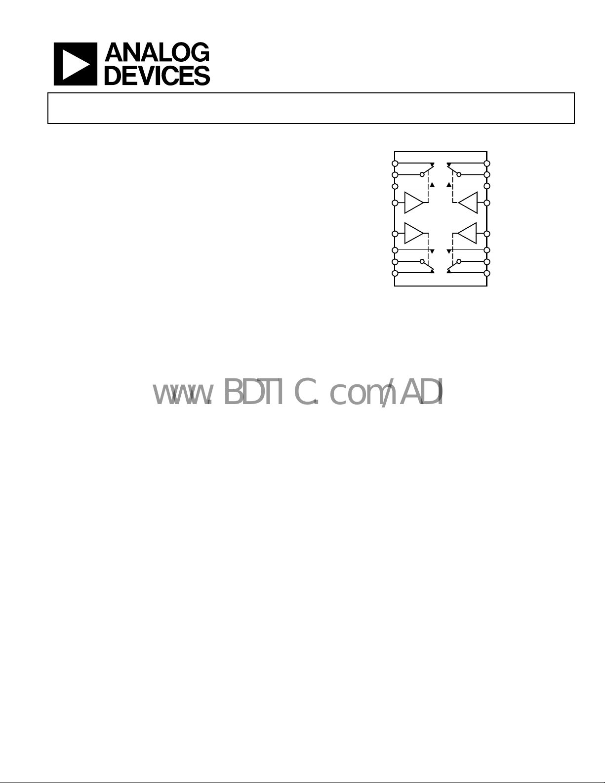
FUNCTIONAL BLOCK DIAGRAM
S1A
D1
S1B
IN1
ADG1334
IN2
S2B
D2
S2A
SWITCHE S SHO WN FOR A LOGIC 1 INPUT
Figure 1.
PRODUCT HIGHLIGHTS
1. 3 V logic compatible digital input V
2. No
V
logic power supply required.
L
3. L
ow power consumption.
4. 20-lead SSO
P.
ADG1334
S4A
D2
S4B
IN4
IN3
S3B
D3
S3A
05744-001
= 2.0 V, VIL = 0.8 V.
IH
Fast switching speed coupled with high signal bandwidth makes
e part suitable for video signal switching. CMOS construction
th
ensures ultra ow power dissipation, making the part ideally
suited for portable and battery-powered instruments.
Rev. 0
Information furnished by Analog Devices is believed to be accurate and reliable. However, no
responsibility is assumed by Anal og Devices for its use, nor for any infringements of patents or ot her
rights of third parties that may result from its use. Specifications subject to change without notice. No
license is granted by implication or otherwise under any patent or patent rights of Analog Devices.
Trademarks and registered trademarks are the property of their respective owners.
One Technology Way, P.O. Box 9106, Norwood, MA 02062-9106, U.S.A.
Tel: 781.329.4700 www.analog.com
Fax: 781.461.3113 ©2006 Analog Devices, Inc. All rights reserved.
Page 2

ADG1334
www.BDTIC.com/ADI
TABLE OF CONTENTS
Features .............................................................................................. 1
Absolute Maximum Ratings ............................................................5
Applications....................................................................................... 1
Functional Block Diagram .............................................................. 1
General Description ......................................................................... 1
Product Highlights ........................................................................... 1
Revision History ............................................................................... 2
Specifications..................................................................................... 3
Dual Supply ................................................................................... 3
Single Supply ................................................................................. 4
REVISION HISTORY
1/06—Revision 0: Initial Version
ESD Caution...................................................................................5
Pin Configuration and Function Descriptions..............................6
Te r mi n ol o g y .......................................................................................7
Typical Perf or m an c e Charac t e r istic s ..............................................8
Test Cir c ui t s..................................................................................... 10
Outline Dimensions ....................................................................... 12
Ordering Guide .......................................................................... 12
Rev. 0 | Page 2 of 12
Page 3
ADG1334
www.BDTIC.com/ADI
SPECIFICATIONS
DUAL SUPPLY1
VDD = +15 V ± 10%, VSS = –15 V ± 10%, GND = 0 V, unless otherwise noted.
Table 1.
B Version
Parameter
+25°C
ANALOG SWITCH
Analog Signal Range VSS to V
On Resistance (RON) 130 230 Ω typ VS = ±10 V, IS = −10 mA; see Figure 11
200 Ω max VDD = +13.5 V, VSS = −13.5 V
On Resistance Match Between Channels (∆RON) 5 Ω typ VS = ±10 V, IS = −10 mA
10 Ω max
On Resistance Flatness (R
) 25 Ω typ VS = −5 V, 0 V, +5 V; IS = −10 mA
FLAT (ON)
65 Ω max
LEAKAGE CURRENTS VDD = +16.5 V, VSS = −16.5 V
Source Off Leakage IS (Off) ±10 nA typ VD = ±10 V; VS = ±10 V; see Figure 12
Drain Off Leakage ID (Off) ±10 nA typ VD = ±10 V; VS = ±10 V; see Figure 12
Channel On Leakage ID, IS (On) ±10 nA typ VS = VD = ±10 V; see Figure 13
DIGITAL INPUTS
Input High Voltage, V
Input Low Voltage, V
Input Current, I
INL
2.0 V min
INH
0.8 V max
INL
or I
±0.005 μA typ VIN = V
INH
±0.1 μA max
Digital Input Capacitance, C
IN
5 pF typ
DYNAMIC CHARACTERISTICS2
T
ON
110 ns typ RL = 300 Ω, CL = 35 pF
130 150 ns max VS = 10 V; see Figure 14
T
65 ns typ RL = 300 Ω, CL = 35 pF
OFF
85 95 ns max VS = 10 V; see Figure 14
T
25 ns typ RL = 300 Ω, CL = 35 pF
BBM
10 ns min VS1 = VS2 = +10 V; see Figure 15
Charge Injection 2 pC typ VS = 0 V, RS = 0 Ω, CL = 1 nF; see Figure 16
Off Isolation 80 dB typ RL = 50 Ω, CL = 5 pF, f = 1 MHz; see Figure 17
Channel-to-Channel Crosstalk 85 dB typ RL = 50 Ω, CL = 5 pF, f = 1 MHz; see Figure 19
−3 dB Bandwidth 700 MHz typ RL = 50 Ω, CL = 5 pF; see Figure 18
CS (Off) 5 pF typ f = 1 MHz; VS = 0 V
CD (Off) 5 pF typ f = 1 MHz; VS = 0 V
CD, CS (On) 10 pF typ f = 1 MHz; VS = 0 V
POWER REQUIREMENTS VDD = +16.5 V, VSS = −16.5 V
IDD 0.002 μA typ Digital inputs = 0 V or V
1 μA max
IDD 260 μA typ Digital inputs = 5 V
400 μA max
I
SS
0.002 μA typ Digital inputs = 0 V or V
1 μA max
ISS 0.002 μA typ Digital inputs = 5 V
1 μA max
1
Temperature range is B Version: −40°C to +105°C.
2
Guaranteed by design, not subject to production test.
−40°C to
+105
°C
DD
Unit Test Conditions/Comments
V
or V
INL
INH
DD
DD
Rev. 0 | Page 3 of 12
Page 4
ADG1334
www.BDTIC.com/ADI
SINGLE SUPPLY1
VDD = 12 V ± 10%, VSS = 0 V, GND = 0 V, unless otherwise noted.
Table 2.
B Version
−40°C to
+105
Parameter +25°C
ANALOG SWITCH
Analog Signal Range 0 to V
On Resistance (RON) 325 520 Ω typ VS = 0 V to10 V, IS = −10 mA; see Figure 11
500 Ω max VDD = 10.8 V, VSS = 0 V
On Resistance Match Between Channels (∆RON) 10 Ω typ VS = 0 V to10 V, IS = −10 mA
20 Ω max
On Resistance Flatness (R
) 65 Ω typ VS = 3 V, 6 V, 9 V, IS = −10 mA
FLAT(ON)
LEAKAGE CURRENTS VDD = 13.2 V
Source Off Leakage IS (Off) ±10 nA typ VS = 1 V/10 V, VD = 10 V/1 V; see Figure 12
Drain Off Leakage ID (Off) ±10 nA typ VS = 1 V/10 V, VD = 10 V/1 V; see Figure 12
Channel On Leakage ID, IS (On) ±10 nA typ VS = VD = 1 V or 10 V, see Figure 13
DIGITAL INPUTS
Input High Voltage, V
Input Low Voltage, V
Input Current, I
or I
INL
INH
INL
INH
2.0 V min
0.8 V max
±0.005 μA typ VIN = V
±0.1 μA max
Digital Input Capacitance, C
DYNAMIC CHARACTERISTICS
T
ON
IN
2
3 pF typ f = 1 MHz
135 ns typ RL = 300 Ω, CL = 35 pF
170 200 ns max VS = 8 V; see Figure 14
T
OFF
95 ns typ RL = 300 Ω, CL = 35 pF
115 140 ns max VS = 8 V; see Figure 14
T
BBM
50 ns typ RL = 300 Ω, CL = 35 pF
10 ns min VS1 = VS2 = 8 V; see Figure 15
Charge Injection 2 pC typ VS = 6 V, RS = 0 Ω, CL = 1 nF; see Figure 16
Off Isolation 80 dB typ RL = 50 Ω, CL = 5 pF, f = 1 MHz; see Figure 17
Channel-to-Channel Crosstalk 85 dB typ RL = 50 Ω, CL = 5 pF, f = 1 MHz; see Figure 19
−3 dB Bandwidth 500 MHz typ RL = 50 Ω, CL = 5 pF; see Figure 18
CS (Off) 5 pF typ f = 1 MHz; VS = 6 V
CD (Off) 5 pF typ f = 1 MHz; VS = 6 V
CD, CS (On) 10 pF typ f = 1 MHz; VS = 6 V
POWER REQUIREMENTS VDD = 13.2 V
I
DD
0.002 μA typ Digital inputs = 0 V or V
1 μA max
I
DD
260 μA typ Digital inputs = 5 V
420 μA max
1
Temperature range is B Version: −40°C to +105°C.
2
Guaranteed by design, not subject to production test.
°C
DD
Unit Test Conditions/Comments
V
or V
INL
INH
DD
Rev. 0 | Page 4 of 12
Page 5

ADG1334
www.BDTIC.com/ADI
ABSOLUTE MAXIMUM RATINGS
TA = 25°C, unless otherwise noted.
Table 3.
Parameter Rating
VDD to V
SS
VDD to GND −0.3 V to +25 V
VSS to GND +0.3 V to −25 V
Analog, Digital Inputs
Continuous Current, S or D 24 mA
Peak Current, S or D (Pulsed at 1 ms,
10% Duty Cycle max)
Operating Temperature Range
Industrial Temperature Range
(B Version)
Storage Temperature Range −65°C to +150°C
Junction Temperature 150°C
SSOP Package
θJA, Thermal Impedance 83.2°C/W
Reflow Soldering Peak Temperature,
Pb-free
1
Overvoltages at A, EN, S, or D are clamped by internal diodes. Current should
be limited to the maximum ratings given.
1
35 V
VSS − 0.3 V to VDD + 0.3 V
or 30 mA, whichever
occurs first
100 mA
−40°C to +105°C
260°C
Stresses above those listed under Absolute Maximum Ratings
ma
y cause permanent damage to the device. This is a stress
rating only; functional operation of the device at these or any
other conditions above those listed in the operational sections
of this specification is not implied. Exposure to absolute
maximum rating conditions for extended periods may affect
device reliability.
Only one absolute maximum rating may be applied at any one
e.
tim
ESD CAUTION
ESD (electrostatic discharge) sensitive device. Electrostatic charges as high as 4000 V readily accumulate on
the human body and test equipment and can discharge without detection. Although this product features
proprietary ESD protection circuitry, permanent damage may occur on devices subjected to high energy
electrostatic discharges. Therefore, proper ESD precautions are recommended to avoid performance
degradation or loss of functionality.
Rev. 0 | Page 5 of 12
Page 6

ADG1334
www.BDTIC.com/ADI
PIN CONFIGURATION AND FUNCTION DESCRIPTIONS
IN1
1
S1A
2
3
D1
S1B
V
GND
S2B
D2
S2A
IN2
ADG1334
4
TOP VIEW
5
(Not to Scale)
SS
6
7
8
9
10
NC = NO CONNECT
Figure 2. 20-Lead SSOP Pin
Table 4. 20-Lead SSOP Pin Function Descriptions
Pin No. Mnemonic Description
1, 10, 11, 20 IN1, IN2, IN3, IN4 Logic Control Input.
2, 4, 7, 9, 12, 14, 17, 19 S1A, S1B, S2B, S2A, S3A, S3B, S4B, S4A Source Terminal. Can be an input or output.
3, 8, 13, 18 D1, D2, D3, D4 Drain Terminal. Can be an input or output.
5 V
SS
6 GND Ground (0 V) Reference.
15 NC No Connect.
16 V
DD
IN4
20
19
S4A
18
D4
S4B
17
16
V
DD
15
NC
S3B
14
D3
13
12
S3A
IN3
11
05744-002
Configuration
Most Negative Power Supply Potential in Dual Supplies. In
single-supply applications, it can be connected to ground.
Most Positive Power Supply Potential.
Table 5. ADG1334 Truth Table
Logic Switch A Switch B
0 Off On
1 On Off
Rev. 0 | Page 6 of 12
Page 7

ADG1334
www.BDTIC.com/ADI
TERMINOLOGY
RON
Ohmic resistance between D and S.
ΔR
ON
Difference between the R
(Off)
I
S
of any two channels.
ON
Source leakage current when switch is off.
I
(Off)
D
Drain leakage current when switch is off.
I
, IS (On)
D
Channel leakage current when switch is on.
V
(VS)
D
Analog voltage on Terminal D, Terminal S.
C
(OFF)
S
Channel input capacitance for off condition.
C
(Off)
D
Channel output capacitance for off condition.
C
, CS (On)
D
On switch capacitance.
C
IN
Digital input capacitance.
t
ON
The delay between applying the digital control input and the
output switching on (see Figure 14).
t
BBM
Off time measured between the 80% point of both switches
when switching from one address state to another.
V
INL
Maximum input voltage for Logic 0.
V
INH
Minimum input voltage for Logic 1.
(I
INL
INH
)
I
Input current of the digital input.
I
DD
Positive supply current.
I
SS
Negative supply current.
Off Isolation
A measure of unwanted signal coupling through an off channel.
Charge Injection
A measure of the glitch impulse transferred from the digital
put to the analog output during switching.
in
Bandwidth
Frequency at which the output is attenuated by 3 dB.
On Response
Frequency response of the on switch.
t
OFF
The delay between applying the digital control input and the
output switching off (see Figure 14).
Rev. 0 | Page 7 of 12
Page 8

ADG1334
www.BDTIC.com/ADI
TYPICAL PERFORMANCE CHARACTERISTICS
200
TA = 25°C
180
160
140
120
100
80
ON RESISTANCE (Ω)
60
40
20
0
–15 –12 –9 –6 –3 3 90 6 12 15
VDD = +15V
= –15V
V
SS
SOURCE OR DRAIN VOLTAGE (V)
05744-007
600
VDD = 12V
= 0V
V
SS
500
TA = +85°C
400
300
200
ON RESISTANCE (Ω)
100
0
0246810
TA = –40°C
SOURCE OR DRAIN VOLTAGE (V)
TA = +25°C
05744-010
12
Figure 3. On Resistance as a Function of V
450
TA = 25°C
400
350
300
250
200
150
ON RESISTANCE (Ω)
100
50
0
0246810
SOURCE OR DRAIN VOLTAGE (V)
VDD = 12V
V
SS
Figure 4. On Resistance as a Function of V
250
VDD = +15V
= –15V
V
SS
200
150
100
ON RESISTANCE (Ω)
50
0
–15 –10 –5 0 5 10 15
TA = +85°C
TA = –40°C
SOURCE OR DRAIN VOLTAGE (V)
Figure 5. On Resistance as a Function of V
(VS ) for Dual Supply
D
= 0V
(VS ) for Single Supply
D
TA = +25°C
(VS ) for Different
D
Temperatures, Dual Supply
05744-008
12
05744-009
Figure 6. On Resistance as a Function of V
(VS ) for Different
D
Temperatures, Single Supply
6
TA = +25°C
4
VDD = +5V
V
2
0
–2
CHARGE INJECTI ON (pC)
–4
–6
–15 –10 –5 0 15105
SS
= –5V
VS (V)
VDD = +15V
V
SS
Figure 7. Charge Injection vs. Source Voltage
160
VDD = +15V
V
= –15V
SS
140
T
120
100
80
TIME (ns)
60
40
20
0
–40 –20 0 20 6040 80
Figure 8. T
TEMPERATURE (°C)
Time vs. Temperature
ON/TOFF
ON
T
OFF
= –15V
VDD = +12V
V
= 0V
SS
05744-011
05744-005
Rev. 0 | Page 8 of 12
Page 9

ADG1334
A
–
www.BDTIC.com/ADI
0
VDD = +15V
–10
V
= –15V
SS
T
= +25°C
A
–20
–30
–40
–50
TION (dB)
–60
–70
OFF ISOL
–80
–90
–100
–110
10k 100k 1M 10M 100M 1G
FREQUENCY (Hz)
05744-006
Figure 9. Off Is olation v s. Frequency
10
–20
–30
–40
–50
–60
CROSSTALK (dB)
–70
–80
–90
–100
10k 100k 1M 10M 100M 1G
FREQUENCY (Hz)
SxA – SxB
S1x – S2x
Figure 10. Cross talk vs. Frequency
VDD = +15V
V
= –15V
SS
T
= +25°C
A
05744-004
Rev. 0 | Page 9 of 12
Page 10

ADG1334
V
VDDV
V
www.BDTIC.com/ADI
TEST CIRCUITS
V
SD
V
S
Figure 11. On Resistance
IS (OFF) ID (OFF)
S
SD
A A
Figure 12. Off Leakage
V
S
V
IN
SxB
SxA
INx
NC
I
DS
05744-017
SD
NC = NO CONNECT
ID (ON)
A
V
D
05744-019
Figure 13. On Leakage
V
D
05744-018
SS
0.1μF0.1μF
V
V
DD
SS
GND
D
R
L
300Ω
C
L
35pF
V
OUT
Figure 14. Switching Timing
V
IN
V
IN
V
OUT
50%
50%
90%
t
ON
50%
50%
90%
t
OFF
05744-020
V
DD
SS
0.1μF0.1μF
V
V
V
DD
SS
SxB
V
S
SxA
INx
V
IN
GND
D
R
L
300Ω
C
L
35pF
V
OUT
IN
80%
V
OUT
t
BBM
t
BBM
05744-021
Figure 15. Break-Before-Make Delay
Rev. 0 | Page 10 of 12
Page 11

ADG1334
VDDV
V
V
V
www.BDTIC.com/ADI
SS
0.1μF0.1μF
VIN(NORMALLY
NC
V
OUT
CLOSED SWITCH)
VIN(NORMALLY
OPEN SWITCH)
V
OUT
ΔV
OUT
Q
INJ
ON
= CL× ΔV
OUT
OFF
05744-023
V
V
DD
SS
GND
SxB
SxA
C
1nF
L
D
V
S
INx
V
IN
Figure 16. Charge Injection
V
DD
0.1μF
V
INx
V
IN
0.1μF
SS
V
DD
SS
SxA
SxB
D
GND
OFF ISOLATION = 20 log
V
DD
SS
0.1μF
NC
50Ω
V
OUT
V
Figure 17. Off Isolation
0.1μF
S
NETWORK
ANALYZER
50Ω
V
OUT
R
L
50Ω
0.1μF
NETWORK
ANALYZER
V
OUT
R
L
V
S
05744-024
CHANNEL-TO-CHANNEL CROS S TALK = 20 l og
50Ω
V
S
SxA
SxB
INx
Figure 19. Channel-to-Channel Crosstalk
V
DD
V
SS
0.1μF
V
DD
GND
V
OUT
V
SS
D
R
50Ω
S
05744-026
V
DD
INx
V
IN
SxA
GND
INSERTION LOSS = 20 log
V
SS
D
SxB
NC
V
V
OUT
Figure 18. Bandwidth
WITH SWITCH
OUT
WITHOUT SWITCH
NETWORK
ANALYZER
50Ω
V
OUT
R
L
50Ω
V
S
05744-025
Rev. 0 | Page 11 of 12
Page 12

ADG1334
www.BDTIC.com/ADI
OUTLINE DIMENSIONS
7.50
7.20
6.90
20 11
5.60
5.30
8.20
5.00
0.25
0.09
SEATING
PLANE
S-20)
7.80
7.40
8°
4°
0°
0.95
0.75
0.55
PIN 1
0.05 MIN
COPLANARITY
0.10
1
2.00 MAX
0.65
BSC
COMPLIANT TO JEDEC STANDARDS MO-150-AE
10
1.85
1.75
1.65
0.38
0.22
Figure 20. 20-Lead Shrink Small Outline Package [SSOP]
(R
Dimensions shown in millimeters
ORDERING GUIDE
Model Temperature Range Description Package Option
ADG1334BRSZ
ADG1334BRSZ-REEL
1
Z = Pb-free part.
1
1
−40°C to +105°C 20-Lead Shrink Small Outline Package (SSOP) RS-20
−40°C to +105°C 20-Lead Shrink Small Outline Package (SSOP) RS-20
©2006 Analog Devices, Inc. All rights reserved. Trademarks and
registered trademarks are the property of their respective owners.
D05744-0-1/06(0)
T
Rev. 0 | Page 12 of 12
TTT
 Loading...