

Page 1
ISM Band
www.BDTIC.com/ADI
FEATURES
Single-chip, low power UHF receiver
Companion receiver to ADF7901 transmitter
Frequency range: 369.5 MHz to 395.9 MHz
Eight RF channels selectable with three digital inputs
Modulation parameters supported
FSK demodulation
2 kbps data rate
34.8 kHz frequency deviation
5.0 V supply voltage
Low power consumption
18.5 mA with receiver enabled
1 μA standby current
24-lead TSSOP
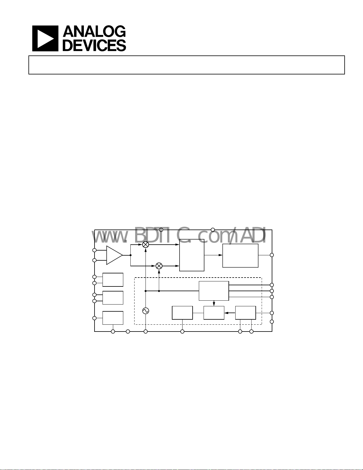
FUNCTIONAL BLOCK DIAGRAM
ADF7902
GENERAL DESCRIPTION
The ADF7902 is a low power UHF receiver. The device demodulates frequency shift keyed (FSK) signals with 34.8 kHz frequency
deviation and at data rates of up to 2 kbps. There are eight specific
RF channels ranging from 369.5 MHz to 395.9 MHz on which the
receiver can operate. Each channel is selectable by configuring
three digital control lines.
The ADF7902 is designed for low power applications, consuming
18.5
mA (typical) during normal operation and 1 μA (maximum)
in standby mode.
GND CE
FSK Receiver IC
ADF7902
LNA_1
LNA_2
VBAT1
CREG1
VBAT2
CREG2
LNA_RSET
LNA
LDO1
LDO2
BIAS
RSET
CVCO
VCOIN
VCO
IF FILTER
CP
CPOUT
Figure 1.
N DIVIDER
SELECT
PFD OSC
FSK
DEMODULATO R
OSC1
OSC2
Rx_DATA
CH1_SEL
CH2_SEL
CH3_SEL
CLKOUT
CLKOUT_ENB
06456-001
Rev. 0
Information furnished by Analog Devices is believed to be accurate and reliable. However, no
responsibility is assumed by Anal og Devices for its use, nor for any infringements of patents or ot her
rights of third parties that may result from its use. Specifications subject to change without notice. No
license is granted by implication or otherwise under any patent or patent rights of Analog Devices.
Trademarks and registered trademarks are the property of their respective owners.
One Technology Way, P.O. Box 9106, Norwood, MA 02062-9106, U.S.A.
Tel: 781.329.4700 www.analog.com
Fax: 781.461.3113 ©2007 Analog Devices, Inc. All rights reserved.
Page 2
ADF7902
www.BDTIC.com/ADI
TABLE OF CONTENTS
Features.............................................................................................. 1
General Description ......................................................................... 1
Functional Block Diagram .............................................................. 1
Revision History ............................................................................... 2
Specifications..................................................................................... 3
Absolute Maximum Ratings............................................................ 4
ESD Caution.................................................................................. 4
Pin Configuration and Function Descriptions............................. 5
REVISION HISTORY
1/07—Revision 0: Initial Version
Typical Performance Characteristics..............................................6
Applications Information.................................................................7
Applications Circuits ....................................................................7
Test Modes..........................................................................................9
Outline Dimensions....................................................................... 10
Ordering Guide .......................................................................... 10
Rev. 0 | Page 2 of 12
Page 3
ADF7902
www.BDTIC.com/ADI
SPECIFICATIONS
VDD =5.0 V; GND = 0 V; TA = T
Table 1.
Parameter Min Typ Max Unit Test Conditions
CHANNEL FREQUENCIES
Channel 1 369.5 MHz
Channel 2 371.1 MHz
Channel 3 375.3 MHz
Channel 4 376.9 MHz
Channel 5 388.3 MHz
Channel 6 391.5 MHz
Channel 7 394.3 MHz
Channel 8 395.9 MHz
RECEIVER PARAMETERS
Data Rate 2 kbps
Frequency Deviation −34.8 kHz Data = 0
+34.8 kHz Data = 1
Input Sensitivity −110 dBm
LNA Input Impedance 128 − j125
CHANNEL FILTERING
IF Filter Bandwidth 200 kHz −3 dB bandwidth
Adjacent Channel Rejection 60 dB 1 MHz offset
PHASE-LOCKED LOOP
CE High to Receive Data 4 ms
REFERENCE INPUT
Crystal Reference 9.8304 MHz ±25 ppm frequency accuracy
INPUT LOGIC LEVELS
Input High Voltage, VIH 0.7 × VDD V
Input Low Voltage, VIL 0.2 × VDD V
OUTPUT LOGIC LEVELS
Output High Voltage, VOH 4.5 V
Output Low Voltage, VOL 0.4 V
Output Drive Level 2 mA
POWER SUPPLY
Voltage Supply
VDD 5 V
Current Consumption
Receiver Enabled 18.5 mA CE = 1
Low Power Sleep Mode 1 μA CE = 0
MIN
to T
, unless otherwise noted. Typical specifications TA = 25°C.
MAX
fRF = 388.3 MHz
Desired signal 3 dB above input sensitivity level,
with in
terferer power increased until BER = 10
−3
Rev. 0 | Page 3 of 12
Page 4
ADF7902
www.BDTIC.com/ADI
ABSOLUTE MAXIMUM RATINGS
TA = 25°C, unless otherwise noted.
Table 2.
Parameter Rating
VBAT to GND
Digital I/O Voltage to GND −0.3 V to VBAT + 0.3 V
LNA_1, LNA_2 0 dBm
Operating Temperature Range
Industrial (B Version) −40°C to +85°C
Storage Temperature Range −40°C to +125°C
Maximum Junction Temperature 125°C
TSSOP θJA Thermal Impedance 150.4°C/W
Lead Temperature, Soldering
Vapor Phase (60 sec) 235°C
Infrared (15 sec) 240°C
1
GND = GND1 = GND1B = GND2 = 0 V.
1
−0.3 V to +6.0 V
Stresses above those listed under Absolute Maximum Ratings
ma
y cause permanent damage to the device. This is a stress
rating only; functional operation of the device at these or any
other conditions above those indicated in the operational
section of this specification is not implied. Exposure to absolute
maximum rating conditions for extended periods may affect
device reliability.
ESD CAUTION
Rev. 0 | Page 4 of 12
Page 5

ADF7902
www.BDTIC.com/ADI
PIN CONFIGURATION AND FUNCTION DESCRIPTIONS
CREG2
TEST
VBAT2
CE
Rx_DATA
GND1
CH1_SEL
CH2_SEL
CLKOUT
CH3_SEL
CLKOUT_ENB
CPOUT
1
2
3
4
5
ADF7902
6
TOP VIEW
7
(Not to Scale)
8
9
10
11
12
24
VCOIN
23
GND2
22
CVCO
21
RSET
20
LNA_RSET
LNA_1
19
18
LNA_2
17
CREG1
VBAT1
16
15
OSC1
14
OSC2
13
GND1B
06456-002
Figure 2. Pin Configuration
Table 3. Pin Function Descriptions
Pin No. Mnemonic Description
1 CREG2
A 0.1 μF capacitor should be added at CREG2 to reduce regulator noise and improve stability. A reduced
capacitor improves regulator power-on time but may cause higher spurs.
2 TEST Test Output Pin. Leave as no connect.
3 VBAT2
5 V Power Supply for RF Circuitry. Decoupling capacitors to the analog ground plane should be placed as close
as possible to this pin.
4 CE Chip Enable Input. Driving CE low puts the part into power-down mode, drawing <1 μA.
5 Rx_DATA Receiver Output. Demodulated data appears on this pin.
6 GND1 Ground for Digital Circuitry.
7 CH1_SEL Channel Select Pin. This represents the LSB of the channel select pins.
8 CH2_SEL Channel Select Pin.
9 CLKOUT
Square Wave Clock Output at the Crystal Frequency. This can be used to dr
ive the OSC2 pin of a partnering
ADF7902. The output has a 50:50 mark-space ratio and switches between 0 V and 2.2 V. If CLKOUT is disabled
by setting Pin 11 high, then CLKOUT must be tied low.
10 CH3_SEL Channel Select Pin.
11 CLKOUT_ENB
CLKOUT Enable Input. This should be driven low to enable
the reference clock signal to appear on the CLKOUT pin.
Driving the pin high removes the clock signal on CLKOUT. It should be driven high when an external reference is used.
12 CPOUT
Charge Pump Output. This output generates current pulses that are integrated in the loop filter. The integrated
current changes the control voltage on the input to the VCO.
13 GND1B Ground for Digital Circuitry.
14 OSC2
The reference crystal should be connected between this pin and OSC1. The necessary crystal load capacitor
should be tied bet
ween this pin and ground. A square wave signal can be applied to this pin as an external
reference source.
15 OSC1
The reference crystal should be connected between this pin and OSC2. The necessary crystal load capacitor
should be tied bet
ween this pin and ground. This pin should be connected to ground when OSC2 is driven by an
external reference.
16 VBAT1
17 CREG1
5 V Power Supply for Digital Circuitry. Decoupling capacitors to the analog ground plane should be placed as
as possible to this pin.
close
A 0.1 μF capacitor should be added at CREG1 to reduce regulator noise and improve stability. A reduced
capacitor improves regulator power-on time but may cause higher spurs.
18 LNA_2
LNA Input. Input matching is required between the antenna and the differential LNA input to e
power transfer.
19 LNA_1 Complementary LNA Input.
20 LNA_RSET
21 RSET
22 CVCO
23
GND2
24 VCOIN
External Bias Resistor for LNA. A value of 1.1 k is recommended.
External Resistor to Set Charge Pump Current and Some Internal Bias Currents. A value of 3.6 k is recommended.
Voltage Controlled Oscillator (VCO) Capacitor. A 22 nF capacitor should be placed between this pin and CREG2
educe VCO noise.
to r
Ground for RF Circuitry.
The tuning voltage on this pin determines the output frequency of the VCO. The higher the tuning voltage,
the higher the output frequency. The output of the loop filter is connected here.
nsure maximum
Rev. 0 | Page 5 of 12
Page 6

ADF7902
www.BDTIC.com/ADI
TYPICAL PERFORMANCE CHARACTERISTICS
70
60
50
40
30
20
REJECTION (d B)
10
CARRIER ONLY
INTERFERER SIGNAL
FSK INTERFERER SIGNAL
0
–1
–2
–3
–4
LOG (BER)
–5
–6
CH0
CH1
CH2
CH3
CH4
CH5
CH6
CH7
0
–10
375.5 376.0 376.50 377.0 377.5 378.0 378.5
FREQUENCY (MHz )
Figure 3. Narrow-Band Interference Rejection Plot
100
CARRIER ONLY
80
60
FSK INTERFERER SIGNAL
40
REJECTION (d B)
20
0
355 365 375 385 395
INTERFERER SIGNAL
FREQUENCY (MHz )
06456-003
06456-004
–7
–8
–125 –120 –115 –110 –105 –100
RF INPUT LEVEL (d Bm)
Figure 5. Sensitivity Plot
06456-005
Figure 4. Wideband Interference Rejection Plot
Rev. 0 | Page 6 of 12
Page 7

ADF7902
F
www.BDTIC.com/ADI
APPLICATIONS INFORMATION
Table 4. Channel Frequency Truth Table
CH1_SEL CH2_SEL CH3_SEL Channel Frequency (MHz)
0 0 0 369.5
1 0 0 371.1
0 0 1 375.3
1 1 0 376.9
0 1 0 388.3
1 0 1 391.5
0 1 1 394.3
1 1 1 395.9
APPLICATIONS CIRCUITS
22n
MICROCONTRO LLER
0.1µF
5V
0.1µF 62pF
VCOIN
GND2
CVCO
RSET
LNA_RSET
LNA_1
LNA_2
CREG1
VBAT1
OSC1
OSC2
GND2
LOOP FILTER
3.6kΩ
1.1kΩ
9.8304MHz
33pF
CRYSTAL
5V
680pF
CREG2
TEST
ADF7902
VBAT2
CE
Rx_DATA
GND1
CH1_SEL
CH2_SEL
CLKOUT
CH3_SEL
CLKOUT_ENB
CPOUT
3.3kΩ
820Ω
15nF 150pF
Figure 6. Single Receiver Applications Circuit
0.1µF
33pF
5V
62pF
MATCHING
10pF
68nH
3.9pF
0.1µF
ANTENNA
06456-006
Rev. 0 | Page 7 of 12
Page 8

ADF7902
F
www.BDTIC.com/ADI
680pF
5V
CREG2
TEST
VBAT2
CE
Rx_DATA
GND1
CH1_SEL
CH2_SEL
CLKOUT
CH3_SEL
CLKOUT _ENB
CPOUT
CREG2
TEST
VBAT2
CE
Rx_DATA
GND1
CH1_SEL
CH2_SEL
CLKOUT
CH3_SEL
CLKOUT _ENB
CPOUT
0.1µF
5V
MICROCONTRO LLER
0.1µF 62pF
0.1µF
5V
0.1µF 62pF
22n
ADF7902
(Rx1)
LNA_RSET
3.3kΩ
820Ω
15nF 150pF
LOOP FILTER
22nF
ADF7902
(Rx2)
LNA_RSET
VCOIN
GND2
CVCO
RSET
LNA_1
LNA_2
CREG1
VBAT1
OSC1
OSC2
GND2
VCOIN
GND2
CVCO
RSET
LNA_1
LNA_2
CREG1
VBAT1
OSC1
OSC2
GND2
3.6kΩ
1.1kΩ
3.6kΩ
1.1kΩ
Y1
33pF
CRYSTAL
5V
0.1µF
62pF
33pF
5V
0.1µF 62pF
MATCHING
6.8pF
62nH
3.9pF
0.1µF
ANTENNA
MATCHI NG
10pF
68nH
3.9pF
0.1µF
3.3kΩ
680pF
820Ω
LOOP FILTER
15nF 150pF
Figure 7. Dual Receiver Applications Circuit
Rev. 0 | Page 8 of 12
6456-007
Page 9

ADF7902
www.BDTIC.com/ADI
TEST MODES
If CLKOUT_ENB is tied high, CLKOUT is disabled. The
CLKOUT pin is reconfigured as a test enable input. If the
CLKOUT pin is then tied low, the part operates as is normal
with CLKOUT off. If it is tied high (2.2 V), the part is in test
mode. Test mode is described in
Table 5. Test Modes
CH1_SEL CH2_SEL CH3_SEL Test Mode
0 0 0 agc gain is set to maximum (filti is also set to maximum on test output pin)
0 0 1 filti on test output pin
0 1 0 filtq on test output pin
0 1 1 Charge pump output is set to maximum (test pin is also tri-state)
1 0 0 Charge pump output is set to minimum (also n-divider output ÷ 2 on test output pin)
1 0 1 Charge pump is tri-state (test pin is also tri-state)
1 1 0 n-divider output ÷ 2 on test output pin
1 1 1 Recovered data clock on test output pin
Tabl e 5 .
When CLKOUT_ENB = 0, RSSI appears on the test output pin
(Pin
2), and CLKOUT is configured as an output with a 9.8 MHz
clock coming out.
When test mode is enabled, the channel frequency is set to
369.5 MH
z (Channel 1).
Rev. 0 | Page 9 of 12
Page 10

ADF7902
www.BDTIC.com/ADI
OUTLINE DIMENSIONS
7.90
7.80
7.70
24
PIN 1
0.15
0.05
0.10 COPLANARITY
0.65
BSC
0.30
0.19
COMPLIANT TO JEDEC STANDARDS MO-153-AD
13
121
1.20
MAX
SEATING
PLANE
4.50
4.40
4.30
6.40 BSC
0.20
0.09
8°
0°
0.75
0.60
0.45
Figure 8. 24-Lead Thin Shrink Small Outline Package [TSSOP]
(RU-24)
Dimensions shown in millimeters
ORDERING GUIDE
Model Temperature Range Package Description Package Option
ADF7902BRUZ
ADF7902BRUZ-RL
ADF7902BRUZ-RL7
1
Z = Pb-free part.
1
1
−40°C to +85°C 24-Lead Thin Shrink Small Outline Package [TSSOP] RU-24
−40°C to +85°C 24-Lead Thin Shrink Small Outline Package [TSSOP], 13’’ REEL RU-24
1
−40°C to +85°C 24-Lead Thin Shrink Small Outline Package [TSSOP], 7’’ REEL RU-24
Rev. 0 | Page 10 of 12
Page 11

ADF7902
www.BDTIC.com/ADI
NOTES
Rev. 0 | Page 11 of 12
Page 12

ADF7902
www.BDTIC.com/ADI
NOTES
©2007 Analog Devices, Inc. All rights reserved. Trademarks and
registered trademarks are the property of their respective owners.
D06456-0-4/07(0)
Rev. 0 | Page 12 of 12
 Loading...