

Page 1
High Performance, ISM Band,
A
www.BDTIC.com/ADI
FEATURES
Low power, low IF transceiver
Frequency bands
431 MHz to 478 MHz
862 MHz to 956 MHz
Data rates supported
0.15 kbps to 200 kbps, FSK
0.15 kbps to 64 kbps, ASK
2.3 V to 3.6 V power supply
Programmable output power
−16 dBm to +13 dBm in 0.3 dBm steps
Receiver sensitivity
−119 dBm at 1 kbps, FSK
−112 dBm at 9.6 kbps, FSK
−106.5 dBm at 9.6 kbps, ASK
Low power consumption
19 mA in receive mode
26.8 mA in transmit mode (10 dBm output)
−3 dBm IIP3 in high linearity mode
FSK/ASK Transceiver IC
ADF7020
On-chip VCO and fractional-N PLL
On-chip 7-bit ADC and temperature sensor
Fully automatic frequency control loop (AFC) compensates
f
or ±25 ppm crystal at 862 MHz to 956 MHz or±50 ppm at
431 MHz to 478 MHz
Digital RSSI
Integrated Tx/Rx switch
Leakage current of <1 μA in power-down mode
APPLICATIONS
Low cost wireless data transfer
Remote control/security systems
Wireless metering
Keyless entry
Home automation
Process and building control
Wireless voice
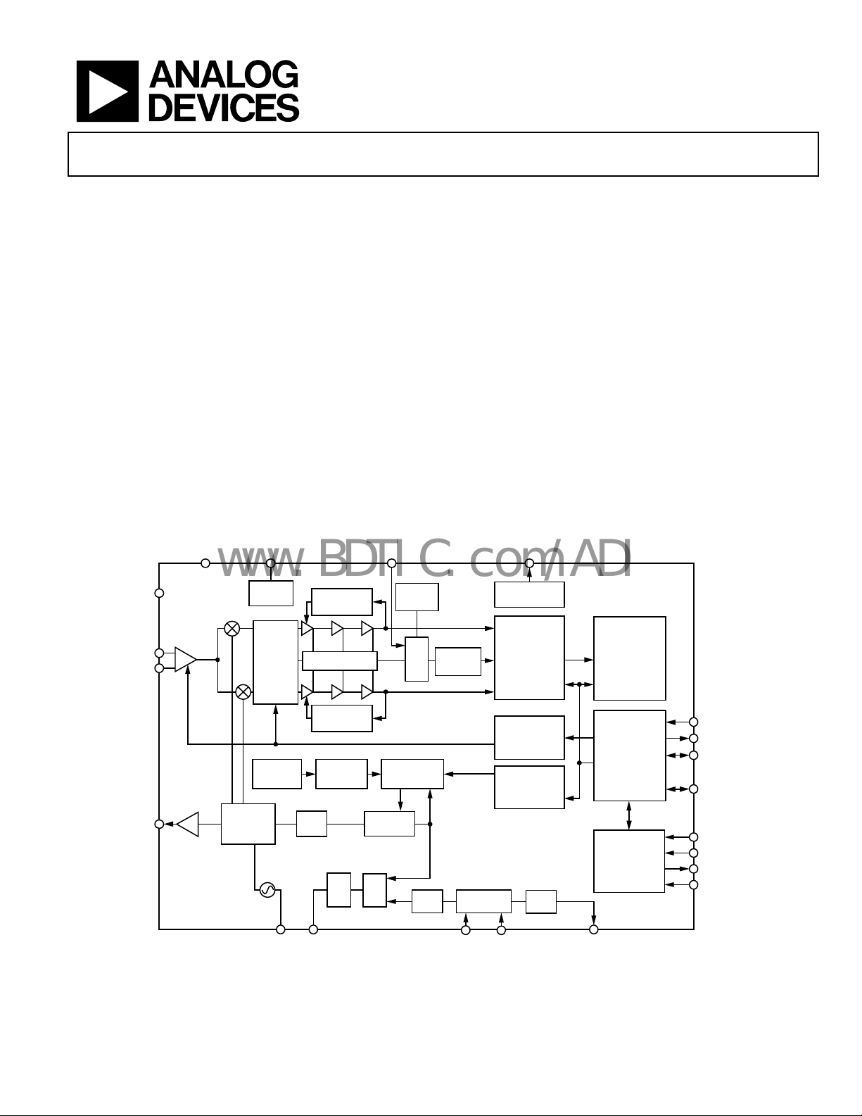
R
LNA
RFIN
RFINB
RFOUT
LNA
GAIN
LDO(1:4)
IF FILTER
FSK MOD
CONTROL
DIVIDERS/
MUXING
VCO
VCOIN CPOUT
FUNCTIONAL BLOCK DIAGRAM
DCINRSET CREG[1:4]
MODULATOR
N/N + 1DIV P
PFD
TEMP
SENSOR
MUX
Σ-Δ
DIV R
7-BIT ADC
Figure 1.
OSC1
OSC
OSC2
OFFSET
CORRECTION
RSSI
OFFSET
CORRECTION
GAUSSIAN
FILTER
CP
MUXOUT
TEST MUX
FSK/ASK
DEMODULATOR
AGC
CONTROL
AFC
CONTROL
CLK
DIV
SYNCHRONIZER
CONTROL
CLKOUT
ADF7020
DATA
Tx/Rx
SERIAL
PORT
CE
DATA CLK
DATA I/O
INT/LOCK
SLE
SDATA
SREAD
SCLK
05351-001
Rev. B
Information furnished by Analog Devices is believed to be accurate and reliable. However, no
responsibility is assumed by Anal og Devices for its use, nor for any infringements of patents or ot her
rights of third parties that may result from its use. Specifications subject to change without notice. No
license is granted by implication or otherwise under any patent or patent rights of Analog Devices.
Trademarks and registered trademarks are the property of their respective owners.
One Technology Way, P.O. Box 9106, Norwood, MA 02062-9106, U.S.A.
Tel: 781.329.4700 www.analog.com
Fax: 781.461.3113 ©2005–2007 Analog Devices, Inc. All rights reserved.
Page 2

ADF7020
www.BDTIC.com/ADI
TABLE OF CONTENTS
Features.............................................................................................. 1
Applications....................................................................................... 1
Functional Block Diagram .............................................................. 1
Revision History ............................................................................... 3
General Description ......................................................................... 4
Specifications..................................................................................... 5
Timing Characteristics..................................................................... 8
Timing Diagrams.......................................................................... 8
Absolute Maximum Ratings.......................................................... 10
ESD Caution................................................................................ 10
Pin Configuration and Function Descriptions........................... 11
Typical Performance Characteristics ........................................... 13
Frequency Synthesizer ................................................................... 15
Reference Input........................................................................... 15
Choosing Channels for Best System Performance................. 17
Transmitter...................................................................................... 18
RF Output Stage.......................................................................... 18
Modulation Schemes.................................................................. 18
Receiver............................................................................................ 20
RF Front End............................................................................... 20
RSSI/AGC.................................................................................... 21
FSK Demodulators on the ADF7020....................................... 21
FSK Correlator/Demodulator................................................... 21
Linear FSK Demodulator .......................................................... 23
AFC .............................................................................................. 23
Automatic Sync Word Recognition .........................................24
Applications Information .............................................................. 25
LNA/PA Matching...................................................................... 25
Image Rejection Calibration ..................................................... 26
Transmit Protocol and Coding Considerations ..................... 27
Device Programming after Initial Power-Up ......................... 27
Interfacing to Microcontroller/DSP ........................................ 27
Power Consumption and battery lifetime calculations......... 28
Serial Interface ................................................................................ 31
Readback Format........................................................................ 31
Registers........................................................................................... 32
Register 0—N Register............................................................... 32
Register 1—Oscillator/Filter Register...................................... 33
Register 2—Transmit Modulation Register (ASK/OOK
Mode)........................................................................................... 34
Register 2—Transmit Modulation Register (FSK Mode) ..... 35
Register 2—Transmit Modulation Register (GFSK/GOOK
Mode)........................................................................................... 36
Register 3—Receiver Clock Register ....................................... 37
Register 4—Demodulator Setup Register ............................... 38
Register 5—Sync Byte Register................................................. 39
Register 6—Correlator/Demodulator Register ...................... 40
Register 7—Readback Setup Register...................................... 41
Register 8—Power-Down Test Register .................................. 42
Register 9—AGC Register......................................................... 43
Register 10—AGC 2 Register.................................................... 44
Register 11—AFC Register ....................................................... 44
Register 12—Test Register......................................................... 45
Register 13—Offset Removal and Signal Gain Register ....... 46
Outline Dimensions....................................................................... 47
Ordering Guide .......................................................................... 47
Rev. B | Page 2 of 48
Page 3

ADF7020
www.BDTIC.com/ADI
REVISION HISTORY
8/07—Rev. A to Rev. B
Changes to Features..........................................................................1
Changes to General Description .....................................................4
Changes to Table 1 ............................................................................5
Changes to Table 2 ............................................................................8
Changes to Reference Input Section .............................................15
Changes to N Counter Section......................................................16
Changes to Choosing Channels for Best Performance Section 17
Changes to Table 5 ..........................................................................20
Changes to FSK Correlator Register Settings Section................22
Added Image Rejection Calibration Section ...............................26
Added Figure 41 ..............................................................................30
Changes to Readback Format Section..........................................31
Changes to Register 9—AGC Register Comments Section.......43
Added Register 12—Test Register Comments Section ..............45
4/06—Rev. 0 to Rev. A
Changes to Features..........................................................................1
Changes to Table 1 ............................................................................5
Changes to Figure 24 ......................................................................17
Changes to the Setting Up the ADF7020 for GFSK Section......19
Changes to Table 6 ..........................................................................21
Changes to Table 9 ..........................................................................23
Changes to External AFC Section.................................................23
Deleted Maximum AFC Range Section.......................................23
Added AFC Performance Section.................................................24
Changes to Internal Rx/Tx Switch Section..................................25
Changes to Figure 32 ......................................................................25
Changes to Transmit Protocol and Coding Considerations
S
ection ..............................................................................................26
Added Text Relating to Figure 37 .................................................27
Changes to Figure 41 ......................................................................31
Changes to Register 1—Oscillator/Filter Register
C
omments........................................................................................31
Changes to Figure 42 ......................................................................32
Changes to Register 2—Transmit Modulation Register
K Mode) Comments ................................................................. 33
(FS
Changes to Figure 44 ......................................................................34
Changes to Register 2—Transmit Modulation Register
(GFS
K/GOOK Mode) Comments................................................34
Changes to Register 4—Demodulator Setup Register
C
omments........................................................................................36
Changes to Figure 51 ......................................................................41
Changes to Figure 53 ......................................................................42
Changes to Ordering Guide...........................................................45
6/05—Revision 0: Initial Version
Rev. B | Page 3 of 48
Page 4

ADF7020
www.BDTIC.com/ADI
GENERAL DESCRIPTION
The ADF7020 is a low power, highly integrated FSK/ASK/OOK
transceiver designed for operation in the license-free ISM bands
at 433 MHz, 868 MHz, and 915 MHz, as well as the proposed
Japanese RFID band at 950 MHz. A Gaussian data filter option
is available to allow either GFSK or G-ASK modulation, which
provides a more spectrally efficient modulation. In addition to
these modulation options, the ADF7020 can also be used to
perform both MSK and GMSK modulation, where MSK is a
special case of FSK with a modulation index of 0.5. The modulation index is calculated as twice the deviation divided by the
data rate. MSK is spectrally equivalent to O-QPSK modulation
with half-sinusoidal Tx baseband shaping, so the ADF7020 can
also support this modulation option by setting up the device in
MSK mode.
This device is suitable for circuit applications that meet the
uropean ETSI-300-220, the North American FCC (Part 15),
E
or the Chinese Short Range Device regulatory standards. A
complete transceiver can be built using a small number of
external discrete components, making the ADF7020 very
suitable for price-sensitive and area-sensitive applications.
The transmitter block on the ADF7020 contains a VCO and
l
ow noise fractional-N PLL with an output resolution of
<1 ppm. This frequency agile PLL allows the ADF7020 to be
used in frequency-hopping spread spectrum (FHSS) systems.
The VCO operates at twice the fundamental frequency to
reduce spurious emissions and frequency-pulling problems.
The transmitter output power is programmable in 0.3 dB steps
f
rom −16 dBm to +13 dBm. The transceiver RF frequency,
channel spacing, and modulation are programmable using a
simple 3-wire interface. The device operates with a power
supply range of 2.3 V to 3.6 V and can be powered down when
not in use.
A low IF architecture is used in the receiver (200 kHz),
mini
mizing power consumption and the external component
count and avoiding interference problems at low frequencies.
The ADF7020 supports a wide variety of programmable
features, including Rx linearity, sensitivity, and IF bandwidth,
allowing the user to trade off receiver sensitivity and selectivity
against current consumption, depending on the application.
The receiver also features a patent-pending automatic frequency
control (AFC) loop, allowing the PLL to track out the frequency
error in the incoming signal.
An on-chip ADC provides readback of an integrated temperat
ure sensor, an external analog input, the battery voltage, or the
RSSI signal, which provides savings on an ADC in some applications. The temperature sensor is accurate to ±10°C over the
full operating temperature range of −40°C to +85°C. This
accuracy can be improved by doing a 1-point calibration at
room temperature and storing the result in memory.
Rev. B | Page 4 of 48
Page 5
ADF7020
www.BDTIC.com/ADI
SPECIFICATIONS
VDD = 2.3 V to 3.6 V, GND = 0 V, TA = T
All measurements are performed using the EVAL-ADF7020DBZx using the PN9 data sequence, unless otherwise noted.
Table 1.
Parameter Min Typ Max Unit Test Conditions
RF CHARACTERISTICS
Frequency Ranges (Direct Output) 862 870 MHz VCO adjust = 0, VCO bias = 10
902 928 MHz VCO adjust = 3, VCO bias = 10
928 956 MHz VCO adjust = 3, VCO bias = 12, VDD = 2.7 V to 3.6 V
Frequency Ranges (Divide-by-2 Mode) 431 440 MHz VCO adjust = 0, VCO bias = 10
440 478 MHz VCO adjust = 3, VCO bias = 12
Phase Frequency Detector Frequency RF/256 24 MHz
TRANSMISSION PARAMETERS
Data Rate
FSK/GFSK 0.15 200 kbps
OOK/ASK 0.15 64
OOK/ASK 0.3 100 kbaud Using Manchester encoding
Frequency Shift Keying
GFSK/FSK Frequency Deviation
4.88 620 kHz PFD = 20 MHz
Deviation Frequency Resolution 100 Hz PFD = 3.625 MHz
Gaussian Filter BT 0.5
Amplitude Shift Keying
ASK Modulation Depth 30 dB
PA Off Feedthrough in OOK Mode −50 dBm
Transmit Power4 −20 +13 dBm VDD = 3.0 V, TA = 25°C
Transmit Power Variation vs.
Temperature
Transmit Power Variation vs. VDD ±1 dB From 2.3 V to 3.6 V at 915 MHz, TA = 25°C
Transmit Power Flatness ±1 dB From 902 MHz to 928 MHz, 3 V, TA = 25°C
Programmable Step Size
−20 dBm to +13 dBm 0.3125 dB
Integer Boundary −55 dBc 50 kHz loop BW
Reference −65 dBc
Harmonics
VCO Frequency Pulling, OOK Mode 30 kHz rms DR = 9.6 kbps
Optimum PA Load Impedance
48 + j54 Ω FRF = 868 MHz
54 + j94 Ω FRF = 433 MHz
RECEIVER PARAMETERS
FSK/GFSK Input Sensitivity At BER = 1E − 3, FRF = 915 MHz,
OOK Input Sensitivity At BER = 1E − 3, FRF = 915 MHz
Second Harmonic −27 dBc Unfiltered conductive
Third Harmonic −21 dBc
All Other Harmonics −35 dBc
Sensitivity at 1 kbps −119.2 dBm FDEV = 5 kHz, high sensitivity mode
Sensitivity at 9.6 kbps −112.8 dBm FDEV = 10 kHz, high sensitivity mode
Sensitivity at 200 kbps −100 dBm FDEV = 50 kHz, high sensitivity mode
Sensitivity at 1 kbps −116 dBm High sensitivity mode
Sensitivity at 9.6 kbps −106.5 dBm High sensitivity mode
2, 3
5
to T
MIN
1 110 kHz PFD = 3.625 MHz
±1 dB From −40°C to +85°C
39 + j61 Ω FRF = 915 MHz
, unless otherwise noted. Typical specifications are at VDD = 3 V, TA = 25°C.
MAX
1
kbps
LNA and PA matched separately
6
7
Rev. B | Page 5 of 48
Page 6
ADF7020
www.BDTIC.com/ADI
Parameter Min Typ Max Unit Test Conditions
LNA and Mixer, Input IP3
Enhanced Linearity Mode −3 dBm Pin = −20 dBm, 2 CW interferers
Low Current Mode −5 dBm FRF = 915 MHz, F1 = FRF + 3 MHz
High Sensitivity Mode −24 dBm F2 = FRF + 6 MHz, maximum gain
Rx Spurious Emissions
−47 dBm >1 GHz at antenna input
AFC
Pull-In Range at 868 MHz/915 MHz ±50 kHz IF_BW = 200 kHz
Pull-In Range at 433 MHz ±25 kHz IF_BW = 200 kHz
Response Time 48 Bits Modulation index = 0.875
Accuracy 1 kHz
CHANNEL FILTERING Desired signal 3 dB above the input sensitivity level,
Adjacent Channel Rejection
(Offset = ±1 × IF Filter BW Setting)
Second Adjacent Channel Rejection
(Offset = ±2 × IF Filter BW Setting)
Third Adjacent Channel Rejection
(Offset = ±3 × IF Filter BW Setting)
Image Channel Rejection
(Uncalibrated)
Image Channel Rejection (Calibrated) 50 dB Image at FRF = 400 kHz
CO-CHANNEL REJECTION −2 dB
Wideband Interference Rejection 70 dB Swept from 100 MHz to 2 GHz, measured as channel
BLOCKING Desired signal 3 dB above the input sensitivity level,
±1 MHz 60 dB
±5 MHz 68 dB
±10 MHz 65 dB
±10 MHz (High Linearity Mode) 72 dB
Saturation (Maximum Input Level) 12 dBm FSK mode, BER = 10−3
LNA Input Impedance 24 − j60 Ω FRF = 915 MHz, RFIN to GND
26 − j63 Ω FRF = 868 MHz
71 − j128 Ω FRF = 433 MHz
RSSI
Range at Input −110 to
Linearity ±2 dB
Absolute Accuracy ±3 dB
Response Time 150 μs
PHASE-LOCKED LOOP
VCO Gain 65 MHz/V 902 MHz to 928 MHz band,
130 MHz/V 860 MHz to 870 MHz band, VCO adjust = 0
65 MHz/V 433 MHz, VCO adjust = 0
Phase Noise (In-Band) −89 dBc/Hz PA = 0 dBm, VDD = 3.0 V, PFD = 10 MHz,
Phase Noise (Out-of-Band) −110 dBc/Hz 1 MHz offset
Residual FM 128 Hz From 200 Hz to 20 kHz, FRF = 868 MHz
PLL Settling 40 μs Measured for a 10 MHz frequency step to within
7
8
−57 dBm <1 GHz at antenna input
CW interferer power level increased until BER = 10
image channel excluded
27 dB IF filter BW settings = 100 kHz, 150 kHz, 200 kHz
50 dB IF filter BW settings = 100 kHz, 150 kHz, 200 kHz
55 dB IF filter BW settings = 100 kHz, 150 kHz, 200 kHz
30 dB Image at FRF = 400 kHz
rejection
CW interferer power level increased until BER = 10
−24
dBm
See the
VCO adjust = 0, VCO_BIAS_SETTING = 10
FRF = 915 MHz, VCO_BIAS_SETTING = 10
5 ppm accuracy, PFD = 20 MHz, LBW = 50 kHz
RSSI/AGC section
−3
−2
,
Rev. B | Page 6 of 48
Page 7

ADF7020
www.BDTIC.com/ADI
Parameter Min Typ Max Unit Test Conditions
REFERENCE INPUT
Crystal Reference 3.625 24 MHz
External Oscillator 3.625 24 MHz
Load Capacitance 33 pF See crystal manufacturer’s specification sheet
Crystal Start-Up Time 2.1 ms 11.0592 MHz crystal, using 33 pF load capacitors
1.0 ms Using 16 pF load capacitors
Input Level CMOS levels
ADC PARAMETERS
INL ±1 LSB From 2.3 V to 3.6 V, TA = 25°C
DNL ±1 LSB From 2.3 V to 3.6 V, TA = 25°C
TIMING INFORMATION
Chip Enabled to Regulator Ready 10 μs C
Chip Enabled to RSSI Ready 3.0 ms
Tx to Rx Turnaround Time 150 μs +
(5 × T
BIT
Time to synchronized data out, includes AGC settling;
)
LOGIC INPUTS
Input High Voltage, V
0.7 ×
INH
V
VDD
Input Low Voltage, V
0.2 ×
INL
V
VDD
Input Current, I
±1 μA
INH/IINL
Input Capacitance, CIN 10 pF
Control Clock Input 50 MHz
LOGIC OUTPUTS
Output High Voltage, VOH DVDD −
V IOH = 500 μA
0.4
Output Low Voltage, VOL 0.4 V IOL = 500 μA
CLK
Rise/Fall 5 ns
OUT
CLK
Load 10 pF
OUT
TEMPERATURE RANGE, TA −40 +85 °C
POWER SUPPLIES
Voltage Supply
VDD 2.3 3.6 V All VDD pins must be tied together
Transmit Current Consumption FRF = 915 MHz, VDD = 3.0 V,
−20 dBm 14.8 mA
−10 dBm 15.9 mA
0 dBm 19.1 mA
10 dBm 28.5 mA
10 dBm 26.8 mA PA matched separately with external antenna
Receive Current Consumption
Low Current Mode 19 mA
High Sensitivity Mode 21 mA
Power-Down Mode
Low Power Sleep Mode 0.1 1 μA
1
Higher data rates are achievable, depending on local regulations.
2
For the definition of frequency deviation, see the Register 2—Transmit Modulation Register (FSK Mode) section.
3
For the definition of GFSK frequency deviation, see the Register 2—Transmit Modulation Register (GFSK/GOOK Mode) section.
4
Measured as maximum unmodulated power. Output power varies with both supply and temperature.
5
For matching details, see the LNA/PA Matching section and the AN-764 Application Note.
6
Sensitivity for combined matching network case is typically 2 dB less than separate matching networks.
7
See Table 5 for a description of different receiver modes.
8
Follow the matching and layout guidelines to achieve the relevant FCC/ETSI specifications.
See the
Reference Input section
= 100 nF
REG
See
Table 11 for more details
see the
AGC Information and Timing section
PA is matched to 50 Ω
Combined PA and LNA matching network as on
EVAL-
ADF7020DBZx boards
VCO_BIAS_SETTING = 12
switch, VCO_BIAS_SETTING = 12
Rev. B | Page 7 of 48
Page 8
ADF7020
www.BDTIC.com/ADI
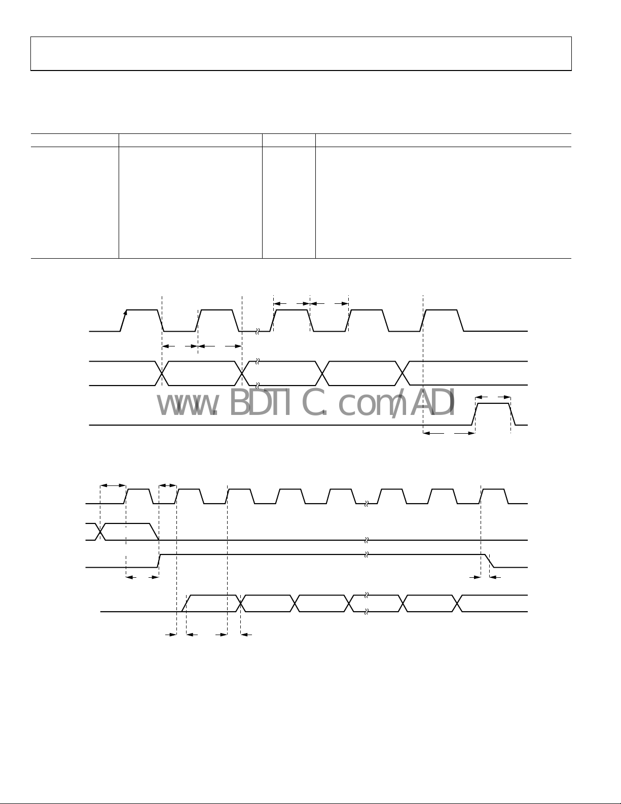
TIMING CHARACTERISTICS
VDD = 3 V ± 10%, VGND = 0 V, TA = 25°C, unless otherwise noted. Guaranteed by design, not production tested.
Table 2.
Parameter Limit at T
t
>10 ns SDATA to SCLK setup time
1
t2 >10 ns SDATA to SCLK hold time
t3 >25 ns SCLK high duration
t4 >25 ns SCLK low duration
t
>10 ns SCLK to SLE setup time
5
t
>20 ns SLE pulse width
6
t
<25 ns SCLK to SREAD data valid, readback
8
t
<25 ns SREAD hold time after SCLK, readback
9
t
>10 ns SCLK to SLE disable time, readback
10
TIMING DIAGRAMS
SCLK
MIN
to T
Unit Test Conditions/Comments
MAX
t
3
t
4
SDATA
SLE
t
1
DB31 (MSB) DB30 DB2
t
2
Figure 2. Serial Interface Timing Diagram
DB1
(CONTROL BIT C2)
DB0 (LSB)
(CONTROL BIT C1)
t
5
t
6
05351-002
SCLK
SDATA
SLE
SREAD
t
1
R7_DB0
(CONTROL BIT C1)
t
2
t
3
X RV16 RV15 RV2 RV1
t
t
8
9
Figure 3. Readback Timing Diagram
t
10
05351-003
Rev. B | Page 8 of 48
Page 9
ADF7020
A
A
www.BDTIC.com/ADI
±1 × DATA RATE/32 1/DATA RAT E
RxCLK
RxDAT
DATA
Figure 4. RxData/RxCLK Timing Diagram
05351-004
1/DATA RATE
TxCLK
TxDAT
NOTES
1. TxCLK ONLY AVAILABLE I N GFSK MODE.
SAMPLEFETCH
DATA
Figure 5. TxData/TxCLK Timing Diagram
5351-005
Rev. B | Page 9 of 48
Page 10

ADF7020
www.BDTIC.com/ADI
ABSOLUTE MAXIMUM RATINGS
TA = 25°C, unless otherwise noted.
Table 3.
Parameter Rating
VDD to GND
Analog I/O Voltage to GND −0.3 V to AVDD + 0.3 V
Digital I/O Voltage to GND −0.3 V to DVDD + 0.3 V
Operating Temperature Range
Industrial (B Version) −40°C to +85°C
Storage Temperature Range −65°C to +125°C
Maximum Junction Temperature 150°C
MLF θJA Thermal Impedance 26°C/W
Reflow Soldering
Peak Temperature 260°C
Time at Peak Temperature 40 sec
1
GND = GND1 = RFGND = GND4 = VCO GND = 0 V.
1
−0.3 V to +5 V
Stresses above those listed under Absolute Maximum Ratings
may cause permanent damage to the device. This is a stress
rating only; functional operation of the device at these or any
other conditions above those indicated in the operational
section of this specification is not implied. Exposure to absolute
maximum rating conditions for extended periods may affect
device reliability.
This device is a high performance RF integrated circuit with an
D rating of <2 kV, and is ESD sensitive. Proper precautions
ES
should be taken for handling and assembly.
ESD CAUTION
Rev. B | Page 10 of 48
Page 11
ADF7020
www.BDTIC.com/ADI
PIN CONFIGURATION AND FUNCTION DESCRIPTIONS
CVCO
GND1
GND
VCO GND
GND
VDD
CPOUT
CREG3
VDD3
OSC1
OSC2
MUXOUT
37
CLKOUT
36
DATA CLK
35
DATA I/O
34
33
INT/LOCK
VDD2
32
CREG2
31
ADCIN
30
GND2
29
SCLK
28
SREAD
27
SDATA
26
SLE
25
VCOIN
CREG1
VDD1
RFOUT
RFGND
RFIN
RFINB
R
LNA
VDD4
RSET
CREG4
GND4
4847464544434241403938
1
2
3
4
5
6
7
8
9
10
11
12
PIN 1
INDICATO R
ADF7020
TOP VIEW
(Not to Scale)
13141516171819
MIX_I
MIX_I
MIX_Q
MIX_Q
FILT_I
GND4
FILT_I
2021222324
GND4
FILT_Q
FILT_Q
TEST_A
CE
05351-006
Figure 6. Pin Configuration
Table 4. Pin Function Descriptions
Pin No. Mnemonic Description
1 VCOIN
The tuning voltage on this pin determines the output frequency of the voltage
-controlled oscillator (VCO).
The higher the tuning voltage, the higher the output frequency.
2 CREG1
3 VDD1
Regulator Voltage for PA Block. A 100 nF in parallel with a 5.1 pF capacitor should be placed between this
pin and gr
Voltage Supply for PA Block. Decoupling capacitors of 0.1 μF an
ound for regulator stability and noise rejection.
d 10 pF should be placed as close as
possible to this pin. All VDD pins should be tied together.
4 RFOUT
The modulated signal is available at this pin. Output po
wer levels are from −20 dBm to +13 dBm. The
output should be impedance matched to the desired load using suitable components. See the Transmitter
sec
tion.
5 RFGND Ground for Output Stage of Transmitter. All GND pins should be tied together.
6 RFIN
LNA Input for Receiver Section. Input matching is requi
red between the antenna and the differential LNA
input to ensure maximum power transfer. See the LNA/PA Matching section.
7 RFINB Complementary LNA Input. See the LNA/PA Matching section.
8 R
External bias resistor for LNA. Optimum resistor is 1.1 kΩ with 5% tolerance.
LNA
9 VDD4 Voltage Supply for LNA/MIXER Block. This pin should be decoupled to ground with a 10 nF capacitor.
10 RSET
External Resistor to Set Charge Pump Current and S
ome Internal Bias Currents. Use 3.6 kΩ with 5%
tolerance.
11 CREG4
Regulator Voltage for LNA/MIXER Block. A 100 nF capacitor should be placed bet
ween this pin and GND
for regulator stability and noise rejection.
12 GND4 Ground for LNA/MIXER Block.
13 to 18
MIX_I, MIX_I
MIX_Q, MIX_Q
FILT_I, FILT_I
Signal Chain Test Pins. These pins are high impedance under normal conditions and should be left
,
unconnected.
,
19, 22 GND4 Ground for LNA/MIXER Block.
20, 21, 23
FILT_Q, FILT_Q
TEST_A
24 CE
25 SLE
,
Signal Chain Test Pins. These pins are high impedance under normal conditions and should be left
unconnected.
Chip Enable. Bringing CE low puts the ADF7020 into complete power-down. Register values are lost when
w, and the part must be reprogrammed once CE is brought high.
CE is lo
Load Enable, CMOS Input. When LE goes high, the data stor
ed in the shift registers is loaded into one of
the fourteen latches. A latch is selected using the control bits.
26 SDATA
Serial Data Input. The serial da
ta is loaded MSB first with the two LSBs as the control bits. This pin is a high
impedance CMOS input.
Rev. B | Page 11 of 48
Page 12

ADF7020
www.BDTIC.com/ADI
Pin No. Mnemonic Description
27 SREAD
28 SCLK
29 GND2 Ground for Digital Section.
30 ADCIN
31 CREG2
32 VDD2
33 INT/LOCK
34 DATA I/O Transmit Data Input/Received Data Output. This is a digital pin, and normal CMOS levels apply.
35 DATA CLK
36 CLKOUT
37 MUXOUT
38 OSC2
39 OSC1 The reference crystal should be connected between this pin and OSC2.
40 VDD3
41 CREG3
42 CPOUT
43 VDD Voltage Supply for VCO Tank Circuit. This pin should be decoupled to ground with a 0.01 μF capacitor.
44 to 47
48 CVCO A 22 nF capacitor should be placed between this pin and CREG1 to reduce VCO noise.
GND, GND1,
O GND
VC
Serial Data Output. This pin is used to feed readback da
SCLK input is used to clock each readback bit (AFC, ADC readback) from the SREAD pin.
Serial Clock Input. This serial clock is used to clock in the ser
the 24-bit shift register on the CLK rising edge. This pin is a digital CMOS input.
Analog-to-Digital Converter Input. The internal 7-bit ADC can be ac
to 1.9 V. Readback is made using the SREAD pin.
Regulator Voltage for Digital Block. A 100 nF in parallel with a 5.
this pin and ground for regulator stability and noise rejection.
Voltage Supply for Digital Block. A decoupling capacitor of 10 nF
this pin.
Bidirectional Pin. In output mode (in
found a match for the preamble sequence. In input mode (lock mode), the microcontroller can be used to
lock the demodulator threshold when a valid preamble has been detected. Once the threshold is locked,
NRZ data can be reliably received. In this mode, a demodulation lock can be asserted with minimum delay.
In receive mode, the pin outputs the synchronized data clock
center of the received data. In GFSK transmit mode, the pin outputs an accurate clock to latch the data
from the microcontroller into the transmit section at the exact required data rate. See the Gaussian
requency Shift Keying (GFSK) section.
F
A Divided-Down Version of the Crystal Reference with O
used to drive several other CMOS inputs, such as a microcontroller clock. The output has a 50:50 markspace ratio.
This pin provides the Lock_Detect signal, which is used t
frequency. Other signals include Regulator_Ready, which is an indicator of the status of the serial interface
regulator.
The reference crystal should be connected between this pin and OSC1. A TCXO reference can be used by
riving this pin with CMOS levels and disabling the crystal oscillator.
d
Voltage Supply for the Charge Pump and PLL Dividers. This pin should be dec
0.01 μF capacitor.
Regulator Voltage for Charge Pump and PLL Dividers. A 100 nF in parallel with a 5.1 pF capacitor should be
ed between this pin and ground for regulator stability and noise rejection.
plac
Charge Pump Output. This output generates current pul
integrated current changes the control voltage on the input to the VCO.
Grounds for VCO Block.
terrupt mode), the ADF7020 asserts the INT/ LOCK pin when it has
ta from the ADF7020 to the microcontroller. The
ial data to the registers. The data is latched into
cessed through this pin. Full scale is 0 V
1 pF capacitor should be placed between
should be placed as close as possible to
. The positive clock edge is matched to the
utput Driver. The digital clock output can be
o determine if the PLL is locked to the correct
oupled to ground with a
ses that are integrated in the loop filter. The
Rev. B | Page 12 of 48
Page 13
ADF7020
–
g
V
Δ
www.BDTIC.com/ADI
TYPICAL PERFORMANCE CHARACTERISTICS
CARRIER POWER
REF –70.00dBc/ Hz
10.00
dB/DIV
0.28dBm ATT EN 0.00dB MKR1
1
10.0000kHz
–87.80dBc/Hz
REF 10dBm
PEAK
lo
10dB/DI
1
REF LEVEL
10.00dBm
ATTEN 20dB
3
4
MKR4 3.482GHz
SWEEP 16.52ms (601pts)
1kHz FREQ UENCY OFFSET
10MHz
05351-007
Figure 7. Phase Noise Response at 868.3 MHz, VDD = 3.0 V, ICP = 1.5 mA
10
20
30
40
50
SIGNAL LE VEL (dBm)
60
70
Figure 8. Output Spectrum in
0
–5
–10
–15
–20
–25
–30
–35
–40
–45
–50
ATTENUATION LEVEL ( dB)
–55
–60
–65
–70
200kHz FILTER BW
GFSK
FREQUENCY (MHz)
150kHz FILT ER BW
IF FREQ (kHz)
Figure 9. IF Fil
FSK and GFSK Modulation
100kHz FILT ER BW
ter Response
PRBS PN9
DR = 7.1kbps
FDEV = 4.88kHz
RBW = 300kHz
FSK
913.38913.28 913.30 913. 32 913. 36
550–350 –250 –150 –50 50 150 250 350 450
05351-008
600–400 –300 –200 –100 0 100 200 300 400 500
05351-009
START 100MHz
RES BW 3MHz
Figure 10. Harmonic Response, RF
REF 15dBm ATTEN 30dB
1R
NORM
log
10dB/DIV
Δ
MARKER
1.834000000GHz
–62.57dB
LgAv
W1 S2
S3 FC
AA
£(f):
FTun
Swp
START 800MHz
#RES BW 30kHz
VBW 3MHz
OUT
1
VBW 30kHz
STOP 10.000GHz
SWEEP 16.52ms (601pts)
Matched to 50 Ω, No Filter
Mkr1 1.834GHz
–62.57dB
STOP 5. 000GHz
SWEEP 5. 627s (601pts)
05351-010
05351-011
Figure 11. Harmonic Response, Murata Dielectric Filter
10
0
–10
–20
–30
SIGNAL LEVEL (dBm)
–40
–50
Figure 12. Output Spectrum in ASK, OOK,
ASK
GOOK
FREQUENCY (MHz)
and GOOK Modes, DR = 10 kbps
OOK
900.80899.60 900.00899.80 900.20 900.40 900.60
05351-012
Rev. B | Page 13 of 48
Page 14
ADF7020
R
R
R
–
www.BDTIC.com/ADI
20
15
10
5
0
–5
–10
PA OUTPUT POWE
–15
–20
–25
1 5 9 13172125293337414549535761
9µA
11µA
7µA
PA SETTING
Figure 13. PA Output Power vs. Setting
5µA
05351-013
BE
0
–1
–2
–3
–4
3.6V, –40°C
–5
–6
–7
–8
–124
DATA RATE = 1kbp s FSK
IF BW = 100kHz
DEMOD BW = 0. 77kHz
2.4V, +85°C
–114
–115
–113
–116
–123
–122
3.0V, +25° C
–121
–120
–119
–118
RF INPUT LEVEL (dBm)
–117
Figure 16. BER vs. VDD and Temperature
–112
–111
–110
–109
–108
–107
–106
05351-016
80
70
60
50
40
30
20
10
LEVEL OF REJECTION (dB)
0
–10
200
250
300
350
400
450
500
550
600
650
700
750
800
850
900
FREQUENCY OF INTERFERER (MHz)
950
1000
1050
1100
Figure 14. Wideband Interference Rejection; Wanted Signal (880 MHz)
3 dB above Sensitivity Point
at
Interferer = FM Jammer (9.76 kbps, 10 kHz Deviation)
20
0
–20
–40
–60
RSSI LEVEL (dB)
–80
–100
–120
ACTUAL INPUT L EVEL
RSSI READBACK LEVEL
20–120 –100 –80 –60 –40 –20 0
RF INPUT (dB)
Figure 15. Digital RSSI Readback Linearity
0
–1
–2
–3
–4
BE
–5
–6
–7
–8
05351-014
1.002k
DATA RATE
–122
–121
–120
–119
–118
–117
–116
–115
–114
–113
–112
RF INPUT LEVEL (d Bm)
–111
–110
–109
9.760k
DATA RATE
Figure 17. BER vs. Data Rate (Comb
200.8k
DATA RATE
–108
–107
–106
–105
–104
–103
–102
–101
–100
ined Matching Network)
–99
–98
–97
–96
–90
–95
–94
–93
–92
–91
05351-017
Separate LNA and PA Matching Paths Typically
Improve Performance by 2 dB
60
–65
–70
–75
–80
–85
–90
–95
SENSITIVITY (dBm)
–100
–105
–110
–90
–110
05351-015
–100
CORRELATOR
AFC ON
CORRELATOR
–70
–50
–80
–30
–60
–40
FREQUENCY ERROR ( kHz)
AFC OFF
0
–10
–20
LINEAR AFC OFF
LINEAR AFC ON
10
30
50
20
40
60
70
90
80
110
100
05351-018
Figure 18. Sensitivity vs. Frequency Error with AFC On/Off
Rev. B | Page 14 of 48
Page 15
ADF7020
P
www.BDTIC.com/ADI
FREQUENCY SYNTHESIZER
REFERENCE INPUT
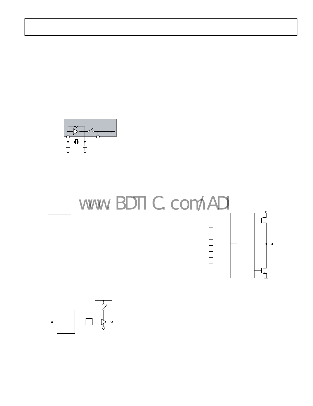
The on-board crystal oscillator circuitry (see Figure 19) can use
an inexpensive quartz crystal as the PLL reference. The oscillator circuit is enabled by setting R1_DB12 high. It is enabled by
default on power-up and is disabled by bringing CE low. Errors
in the crystal can be corrected using the automatic frequency
control (see the
f
ractional-N value (see the N Counter section). A single-ended
r
eference (TCXO, CXO) can also be used. The CMOS levels
should be applied to OSC2 with R1_DB12 set low.
Two parallel resonant capacitors are required for oscillation at
the correct frequency; their values are dependent on the crystal
specification. They should be chosen so that the series value of
capacitance added to the PCB track capacitance adds up to the
load capacitance of the crystal, usually 20 pF. PCB track
capacitance values might vary from 2 pF to 5 pF, depending on
board layout. Thus, CP1 and CP2 can be calculated using:
C +
L
Where possible, choose capacitors that have a low temperature
efficient to ensure stable frequency operation over all
co
conditions.
CLKOUT Divider and Buffer
The CLKOUT circuit takes the reference clock signal from the
oscillator section, shown in Figure 19, and supplies a divideddo
wn 50:50 mark-space signal to the CLKOUT pin. An even
divide from 2 to 30 is available. This divide number is set in
R1_DB[8:11]. On power-up, the CLKOUT defaults to
divide-by-8.
To disable CLKOUT, set the divide number to 0. The output
buffer can drive up to a 20 pF load with a 10% rise time at
4.8 MHz. Faster edges can result in some spurious feedthrough
to the output. A small series resistor (50 Ω) can be used to slow
the clock edges to reduce these spurs at f
AFC section) feature or by adjusting the
OSC1
Figure 19. Oscillator Circuit on the ADF7020
1
=
1
1
+
1
CP2C
DIVIDER
1 TO 15
Figure 20. CLKOUT Stage
OSC2
CP1CP2
C
PCB
DV
DD
÷2
CLK
.
05351-019
CLKOUT
ENABLE BIT
CLKOUTOSC1
05351-020
R Counter
The 3-bit R counter divides the reference input frequency by an
integer ranging from 1 to 7. The divided-down signal is
presented as the reference clock to the phase frequency detector
(PFD). The divide ratio is set in Register 1. Maximizing the
PFD frequency reduces the N value. Every doubling of the PFD
gives a 3 dB benefit in phase noise, as well as reducing
occurrences of spurious components. The R register defaults to
R = 1 on power-up.
PFD [Hz] = XTAL/R
MUXOUT and Lock Detect
The MUXOUT pin allows the user to access various digital
points in the ADF7020. The state of MUXOUT is controlled by
Bits R0_DB[29:31].
Regulator Ready
Regulator ready is the default setting on MUXOUT after the
transceiver has been powered up. The power-up time of the
regulator is typically 50 μs. Because the serial interface is
powered from the regulator, the regulator must be at its
nominal voltage before the ADF7020 can be programmed. The
status of the regulator can be monitored at MUXOUT. When
the regulator ready signal on MUXOUT is high, programming
of the ADF7020 can begin.
DV
DD
REGULATOR READY
DIGITAL LOCK DETECT
ANALOG LO CK DETECT
R COUNTER OUTPUT
N COUNTER OUTPUT
PLL TEST MODES
Σ-Δ TEST MODES
MUX CONTROL
Figure 21. MUXOUT Circuit
MUXOUT
DGND
Digital Lock Detect
Digital lock detect is active high. The lock detect circuit is
located at the PFD. When the phase error on five consecutive
cycles is less than 15 ns, lock detect is set high. Lock detect
remains high until 25 ns phase error is detected at the PFD.
Because no external components are needed for digital lock
detect, it is more widely used than analog lock detect.
Analog Lock Detect
This N-channel open-drain lock detect should be operated with
an external pull-up resistor of 10 kΩ nominal. When a lock has
been detected, this output is high with narrow low going pulses.
05351-021
Rev. B | Page 15 of 48
Page 16

ADF7020
www.BDTIC.com/ADI
Voltage Regulators
The ADF7020 contains four regulators to supply stable voltages
to the part. The nominal regulator voltage is 2.3 V. Each
regulator should have a 100 nF capacitor connected between
CREGx and GND. When CE is high, the regulators and other
associated circuitry are powered on, drawing a total supply
current of 2 mA. Bringing the chip-enable pin low disables the
regulators, reduces the supply current to less than 1 μA, and
erases all values held in the registers. The serial interface
operates off a regulator supply; therefore, to write to the part,
the user must have CE high and the regulator voltage must be
stabilized. Regulator status (CREG4) can be monitored using
the regulator ready signal from MUXOUT.
Loop Filter
The loop filter integrates the current pulses from the charge
pump to form a voltage that tunes the output of the VCO to the
desired frequency. It also attenuates spurious levels generated by
VCO
Figure 22.
05351-022
the PLL. A typical loop filter design is shown in
CHARGE
PUMP OUT
Figure 22. Typical Loop Filter Configuration
In FSK, the loop should be designed so that the loop bandwidth
(LBW) is approximately one and a half times the data rate.
Widening the LBW excessively reduces the time spent jumping
between frequencies, but it can cause insufficient spurious
attenuation.
For ASK systems, a wider LBW is recommended. The sudden
la
rge transition between two power levels can result in VCO
pulling and can cause a wider output spectrum than is desired.
By widening the LBW to more than 10 times the data rate, the
amount of VCO pulling is reduced, because the loop settles
quickly back to the correct frequency. The wider LBW can
restrict the output power and data rate of ASK-based systems
compared with FSK-based systems.
Narrow-loop bandwidths can result in the loop taking long
eriods of time to attain lock. Careful design of the loop filter is
p
critical to obtaining accurate FSK/GFSK modulation.
For GFSK, it is recommended that an LBW of 1.0 to 1.5 times
he data rate be used to ensure that sufficient samples are
t
taken of the input data while filtering system noise. The free
design tool ADI SRD Design Studio™ can be used to design loop
ilters for the ADF7020. It can also be used to view the effect of
f
loop filter bandwidth on the spectrum of the transmitted signal
for different combinations of modulation type, data rates, and
modulation indices.
N Counter
The feedback divider in the ADF7020 PLL consists of an 8-bit
integer counter and a 15-bit Σ-Δ fractional-N divider. The
integer counter is the standard pulse-swallow type common in
PLLs. This sets the minimum integer divide value to 31. The
fractional divide value gives very fine resolution at the output,
where the output frequency of the PLL is calculated as
__NFractional
OUT
REFERENCE IN
4÷R
⎛
⎜
⎝
PFD/
CHARGE
PUMP
Figure 23. Fractional-N PLL
+×=
NIntegerPFDf
THIRD-ORDER
Σ-Δ MODULATOR
2
⎞
⎟
15
⎠
VCO
4÷N
INTEGER-NFRACTIONAL -N
05351-023
The maximum N divide value is the combination of the
Integer_N (maximum = 255) and the Fractional_N (maximum
= 32767/32768) and puts a lower limit on the minimum
usable PFD.
PFD
[Hz] = Maximum Required Output Frequency/(255 + 1)
MIN
For example, when operating in the European 868 MHz to
870 MH
z band, PFD
equals 3.4 MHz. In the majority of
MIN
cases, it is advisable to use as high a value of PFD as possible
to obtain best phase noise performance.
Voltage Controlled Oscillator (VCO)
To minimize spurious emissions, the on-chip VCO operates
from 1724 MHz to 1912 MHz. The VCO signal is then divided
by 2 to give the required frequency for the transmitter and the
required LO frequency for the receiver.
The VCO should be recentered, depending on the required
requency of operation, by programming the VCO Adjust Bits
f
R1_DB[20:21].
The VCO is enabled as part of the PLL by the PLL Enable bit,
B28.
R0_D
A further frequency divide-by-2 block is included to allow
peration in the lower 433 MHz and 460 MHz bands. To enable
o
operation in these bands, R1_DB13 should be set to 1. The
VCO needs an external 22 nF between the VCO and the
regulator to reduce internal noise.
Rev. B | Page 16 of 48
Page 17

ADF7020
www.BDTIC.com/ADI
VCO Bias Current
VCO bias current can be adjusted using Bit R1_DB19 to
Bit R1_DB16. To ensure VCO oscillation, the minimum bias
current setting under all conditions is 0xA.
VCO BIAS
R1_DB[16:19]
LOOP FILTER
CVCO PI N
VCO
220µF
Figure 24. Voltage-Controlled Oscillator (VCO)
DIVIDER
÷2
TO N
÷2
VCO SELECT BIT
MUX
TO PA
05351-024
CHOOSING CHANNELS FOR BEST SYSTEM PERFORMANCE
The fractional-N PLL allows the selection of any channel within
868 MHz to 956 MHz (and 433 MHz using divide-by-2) to a
resolution of <300 Hz. This also facilitates frequency-hopping
systems.
Careful selection of the XTAL frequency is important to achieve
est spurious and blocking performance. The architecture of
b
fractional-N causes some level of the nearest integer channel to
couple directly to the RF output. This phenomenon is often
referred to as integer boundary spurious. If the desired RF channel
and the nearest integer channel are separated by a frequency of
less than the PLL loop bandwidth (LBW), the integer boundary
spurs are not attenuated by the loop.
Integer boundary spurs can be significantly reduced in amplit
ude by choosing XTAL values that place the wanted RF
channel away from integer multiples of the PFD.
Rev. B | Page 17 of 48
Page 18

ADF7020
www.BDTIC.com/ADI
TRANSMITTER
RF OUTPUT STAGE
The PA of the ADF7020 is based on a single-ended, controlled
current, open-drain amplifier that has been designed to deliver
up to 13 dBm into a 50 Ω load at a maximum frequency of
956 MHz.
The PA output current and, consequently, the output power are
rogrammable over a wide range. The PA configurations in
p
FSK/GFSK and ASK/OOK modulation modes are shown in
Figure 25 and Figure 26, respectively. In FSK/GFSK modulation
ode, the output power is independent of the state of the
m
DATA I/O pin. In ASK/OOK modulation mode, it is dependent
on the state of the DATA I/O pin and Bit R2_DB29, which
selects the polarity of the TxData input. For each transmission
mode, the output power can be adjusted as follows:
• FSK/GFSK
The output power is set using Bits R2_DB[9:14].
• ASK
The output power for the inactive state of the TxData input
is set by Bits R2_DB[15:20]. The output power for the
active state of the TxData input is set by Bits R2_DB[9:14].
• OOK
The output power for the active state of the TxData input
is set by Bits R2_DB[9:14]. The PA is muted when the TxData
input is inactive.
R2_DB[30:31]
2
IDAC
6
R2_DB[9:14]
The PA is equipped with overvoltage protection, which makes it
robust in severe mismatch conditions. Depending on the application, one can design a matching network for the PA to exhibit
optimum efficiency at the desired radiated output power level
for a wide range of different antennas, such as loop or monopole antennas. See the
LNA/PA Matching section for details.
PA Bias Currents
Control Bits R2_DB[30:31] facilitate an adjustment of the PA
bias current to further extend the output power control range,
if necessary. If this feature is not required, the default value of
7 μA is recommended. The output stage is powered down by
resetting Bit R2_DB4. To reduce the level of undesired spurious
emissions, the PA can be muted during the PLL lock phase by
toggling this bit.
MODULATION SCHEMES
Frequency Shift Keying (FSK)
Frequency shift keying is implemented by setting the N value
for the center frequency and then toggling this with the TxData
line. The deviation from the center frequency is set using
Bits R2_DB[15:23]. The deviation from the center frequency
in Hz is
FSK
DEVIATION
where
Modulation Number is a number from 1 to 511
]Hz[
×
=
(R2_DB[15:23]).
Select FSK using Bits R2_DB[6:8].
NumberModulationPFD
14
2
RFOUT
RFGND
DATA I/O
RFOUT
RFGND
+
FROM VCO
Figure 25. PA Configuration in FSK/GFSK Mode
R2_DB29
R2_DB[30:31]
IDAC
+
FROM VCO
Figure 26. PA Configuration in ASK/OOK Mode
ASK/OOK MO DE
6
R2_DB4
R2_DB5
DIGITAL
LOCK DETECT
6
R2_DB[9:14]
6
R2_DB[15:23]
0
R2_DB4
R2_DB5
DIGITAL
LOCK DETECT
05351-025
05351-026
Rev. B | Page 18 of 48
FSK DEVIAT ION
TxDATA
FREQUENCY
–
f
DEV
+
f
DEV
PFD/
4R
CHARGE
PUMP
Figure 27. FSK Implementation
THIRD-ORDER
Σ-Δ MODULATOR
PA STAGE
VCO
÷N
INTEGER-NFRACTI ONAL-N
05351-027
Page 19

ADF7020
www.BDTIC.com/ADI
Gaussian Frequency Shift Keying (GFSK)
Gaussian frequency shift keying reduces the bandwidth occupied by the transmitted spectrum by digitally prefiltering the
TxData. A TxCLK output line is provided from the ADF7020
for synchronization of TxData from the microcontroller.
The TxCLK line can be connected to the clock input of a shift
register that clocks data to the transmitter at the exact data rate.
Setting Up the ADF7020 for GFSK
To set up the frequency deviation, set the PFD and the modulation control bits.
m
PFD
×
GFSK
DEVIATION
m is GFSK_Mod_Control, set using R2_DB[24:26].
where
To set up the GFSK data rate,
DR__]bps[×=
The INDEX_COUNTER variable controls the number of interm
ediate frequency steps between the low and high frequency.
It is usually possible to achieve a given data rate with various
combinations of DIVIDER_FACTOR and INDEX_COUNTER.
Choosing a higher INDEX_COUNTER can help in improving
the spectral performance.
=
]Hz[
2
12
2
PFD
COUNTERINDEXFACTORDIVIDER
Amplitude Shift Keying (ASK)
Amplitude shift keying is implemented by switching the output
stage between two discrete power levels. This is accomplished
by toggling the DAC, which controls the output level between
two 6-bit values set up in Register 2. A 0 TxData bit sends
Bits R2_DB[15:20] to the DAC. A high TxData bit sends
Bits R2_DB[9:14] to the DAC. A maximum modulation depth
of 30 dB is possible.
On-Off Keying (OOK)
On-off keying is implemented by switching the output stage to a
certain power level for a high TxData bit and switching the
output stage off for a zero. For OOK, the transmitted power for
a high input is programmed using Bits R2_DB[9:14].
Gaussian On-Off Keying (GOOK)
Gaussian on-off keying represents a prefiltered form of OOK
modulation. The usually sharp symbol transitions are replaced
with smooth Gaussian filtered transitions, the result being a
reduction in frequency pulling of the VCO. Frequency pulling
of the VCO in OOK mode can lead to a wider than desired
BW, especially if it is not possible to increase the loop filter
BW > 300 kHz. The GOOK sampling clock samples data at the
data rate (see the
Setting Up the ADF7020 for GFSK section).
Rev. B | Page 19 of 48
Page 20

ADF7020
T
www.BDTIC.com/ADI
RECEIVER
RF FRONT END
The ADF7020 is based on a fully integrated, low IF receiver
architecture. The low IF architecture facilitates a very low
external component count and does not suffer from power lineinduced interference problems.
Figure 28 shows the structure of the receiver front end. The
any programming options allow users to trade off sensitivity,
m
linearity, and current consumption against each other in the
way best suitable for their applications. To achieve a high level
of resilience against spurious reception, the LNA features a
differential input. Switch SW2 shorts the LNA input when
transmit mode is selected (R0_DB27 = 0). This feature facilitates the design of a combined LNA/PA matching network,
avoiding the need for an external Rx/Tx switch. See the
LNA/PA Matching section for details on the design of the
atching network.
m
I (TO FILTER)
LO
Q (TO FILTER)
MIXER LINE ARITY
(R6_DB18)
(R0_DB27)
LNA CURRENT
(R6_DB[16:17])
(R9_DB[20:21])
RFIN
RFINB
LNA MODE
(R6_DB15)
LNA GAIN
(R8_DB6)
SW2 LNA
Figure 28. ADF7020 RF Front End
x/Rx SELECT
LNA/MIXER E NABLE
The LNA is followed by a quadrature down conversion mixer,
that converts the RF signal to the IF frequency of 200 kHz.
It is important to consider that the output frequency of the
synthesizer must be programmed to a value 200 kHz below
the center frequency of the received channel.
05351-028
The LNA has two basic operating modes: high gain/low noise
m
ode and low gain/low power mode. To switch between these
two modes, use the LNA_Mode bit, R6_DB15. The mixer is also
configurable between a low current and an enhanced linearity
mode using the mixer_linearity bit, R6_DB18.
Based on the specific sensitivity and linearity requirements
o
f the application, it is recommended to adjust control bits
LNA_Mode (R6_DB15) and Mixer_Linearity (R6_DB18), as
outlined in
Tabl e 5 .
The gain of the LNA is configured by the LNA_Gain field,
R9_D
B[20:21], and can be set by either the user or the
automatic gain control (AGC) logic.
IF Filter Settings/Calibration
Out-of-band interference is rejected by means of a fourth-order
Butterworth polyphase IF filter centered around a frequency of
200 kHz. The bandwidth of the IF filter can be programmed
between 100 kHz and 200 kHz by using Control Bits R1_DB[22:23]
and should be chosen as a compromise between interference rejection, attenuation of the desired signal, and the AFC pull-in range.
To compensate for manufacturing tolerances, the IF filter
s
hould be calibrated once after power-up. The IF filter calibration logic requires that the IF filter divider in Bits R6_DB[20:28]
be set as dependent on the crystal frequency. Once initiated
by setting Bit R6_DB19, the calibration is performed
automatically without any user intervention. The calibration
time is 200 μs, during which the ADF7020 should not be
accessed. It is important not to initiate the calibration cycle
before the crystal oscillator has fully settled. If the AGC loop is
disabled, the gain of IF filter can be set to three levels using the
Filter_Gain field, R9_DB[20:21]. The filter gain is adjusted
automatically, if the AGC loop is enabled.
Table 5. LNA/Mixer Modes
Mixer
LNA Mode
Receiver Mode
High Sensitivity Mode (Default) 0 30 0 −110.5 21 −24
RxMode2 1 10 0 −104 20 −13.5
Low Current Mode 1 3 0 −94 19
Enhanced Linearity Mode 1 3 1 −88 19
RxMode5 1 10 1 −98 20
RxMode6 0 30 1 −107 21 −20
(R6_DB15)
LNA Gain Value
(R9_DB[20:21]
Linearit
)
(R6_DB18)
Rev. B | Page 20 of 48
Sensitivity
y
(DR = 9.6 kbps,
f
DEV
= 10 kHz)
Rx Current
C
onsumption
(mA)
Input IP3
(dBm)
−5
−3
−10
Page 21

ADF7020
=
www.BDTIC.com/ADI
RSSI/AGC
The RSSI is implemented as a successive compression log amp
following the baseband channel filtering. The log amp achieves
±3 dB log linearity. It also doubles as a limiter to convert the
signal-to-digital levels for the FSK demodulator. The RSSI itself
is used for amplitude shift keying (ASK) demodulation. In ASK
mode, extra digital filtering is performed on the RSSI value.
Offset correction is achieved using a switched capacitor integrator in feedback around the log amp. This uses the baseband
offset clock divide. The RSSI level is converted for user
readback and digitally controlled AGC by an 80-level (7-bit)
flash ADC. This level can be converted to input power in dBm.
OFFSET
CORRECTION
FSK
1
FWR
FWR FWR FWR
R
NOTES
1. FWR = FULL WAVE RECTIFIER
Figure 29. RSSI Block Diagram
LATCHAAA
CLK
RSSI Thresholds
When the RSSI is above AGC_HIGH_THRESHOLD, the gain
is reduced. When the RSSI is below AGC_LOW_THRESHOLD,
the gain is increased. A delay (AGC_DELAY) is programmed
to allow for settling of the loop. The user programs the two
threshold values (recommended defaults of 30 and 70) and the
delay (default of 10). The default AGC setup values should be
adequate for most applications. The threshold values must be
chosen to be more than 30 apart for the AGC to operate
correctly.
Offset Correction Clock
In Register 3, the user should set the BB offset clock divide bits
R3_DB[4:5] to give an offset clock between 1 MHz and 2 MHz.
BBOS_CLK (Hz) = XTAL/(BBOS_CLK_DIVIDE)
BBOS_CLK_DIVIDE can be set to 4, 8, or 16.
where
AGC Information and Timing
AGC is selected by default, and operates by selecting the appropriate LNA and filter gain settings for the measured RSSI level. It
is possible to disable AGC by writing to Register 9 if entering
one of the modes listed in Tab l e 5 is desired, for example. The
ime for the AGC circuit to settle and, therefore, the time to
t
take an accurate RSSI measurement is typically 150 μs, although
this depends on how many gain settings the AGC circuit has to
cycle through. After each gain change, the AGC loop waits for
a programmed time to allow transients to settle.
DEMOD
ADC
RSSI
ASK
DEMOD
05351-029
This wait time can be adjusted to speed up this settling by
justing the appropriate parameters.
ad
TimeWaitAGC
__
CLKSEQDELAYAGC
__
×
XTAL
AGC Settling = AGC_Wait_Time × Number of Gain Changes
Thus, in the worst case, if the AGC loop has to go through all
5
gain changes, AGC_Delay =10, SEQ_CLK = 200 kHz, AGC
Settling
= 10 × 5 μs × 5 = 250 μs. Minimum AGC_Wait_Time
needs to be at least 25 μs.
RSSI Formula (Converting to dBm)
Input_Power [dBm] = −120 dBm + (Readback_Code +
Gain_Mode_Correction) × 0.5
where:
Readback_Code is given by Bit RV7 to Bit RV1 in the readback
register (see the Readback Format section).
Gain_Mode_Correction is given by the values in Tabl e 6.
LNA gain and filter gain (LG2/LG1, FG2/FG1) are also
btained from the readback register.
o
Table 6. Gain Mode Correction
LNA Gain
(LG2, LG1)
H (1,1) H (1,0) 0
M (1,0) H (1,0) 24
M (1,0) M (0,1)
M (1,0) L (0,0)
L (0,1) L (0,0)
EL (0,0) L (0,0) 105
Filter Gain
(FG2, FG1)
Gain Mode Correction
45
63
90
An additional factor should be introduced to account for losses
in the front-end matching network/antenna.
FSK DEMODULATORS ON THE ADF7020
The two FSK demodulators on the ADF7020 are
• FSK correlator/demodulator
• Linear demodulator
Select these using the demodulator select bits, R4_DB[4:5].
FSK CORRELATOR/DEMODULATOR
The quadrature outputs of the IF filter are first limited and then
fed to a pair of digital frequency correlators that perform bandpass filtering of the binary FSK frequencies at (IF + f
(IF − f
). Data is recovered by comparing the output levels
DEV
from each of the two correlators. The performance of this frequency discriminator approximates that of a matched filter
detector, which is known to provide optimum detection in
the presence of additive white Gaussian noise (AWGN).
DEV
) and
Rev. B | Page 21 of 48
Page 22

ADF7020
R
www.BDTIC.com/ADI
I
LIMITERS
Q
FREQUENCY CORREL ATOR
IF
IF –
f
IF +
DEV
R6_DB[4:13]
R6_DB[14]
Figure 30. FSK Correlator/Demodulator Block Diagram
f
DEV
SLICE
RxDATA
POST
DEMOD FI LTER
0
DATA
SYNCHRONIZER
R3_DB[8:15]
RxCLK
Postdemodulator Filter
A second-order, digital low-pass filter removes excess noise from
the demodulated bit stream at the output of the discriminator.
The bandwidth of this postdemodulator filter is programmable
and must be optimized for the user’s data rate. If the bandwidth
is set too narrow, performance is degraded due to intersymbol
interference (ISI). If the bandwidth is set too wide, excess noise
degrades the receiver’s performance. Typically, the 3 dB bandwidth
of this filter is set at approximately 0.75 times the user’s data rate,
using Bits R4_DB[6:15].
Bit Slicer
The received data is recovered by the threshold detecting the
output of the postdemodulator low-pass filter. In the correlator/
demodulator, the binary output signal levels of the frequency
discriminator are always centered on 0. Therefore, the slicer
threshold level can be fixed at 0, and the demodulator performance is independent of the run-length constraints of the transmit
data bit stream. This results in robust data recovery, which does
not suffer from the classic baseline wander problems that exist in
the more traditional FSK demodulators.
Frequency errors are removed by an internal AFC loop that
measures the average IF frequency at the limiter output and
applies a frequency correction value to the fractional-N
synthesizer. This loop should be activated when the frequency
errors are greater than approximately 40% of the transmit
frequency deviation (see the
AFC section).
Data Synchronizer
An oversampled digital PLL is used to resynchronize the
received bit stream to a local clock. The oversampled clock rate
of the PLL (CDR_CLK) must be set at 32 times the data rate.
See the Register 3—Receiver Clock Register Comments section
fo
r a definition of how to program. The clock recovery PLL can
accommodate frequency errors of up to ±2%.
FSK Correlator Register Settings
To enable the FSK correlator/demodulator, Bits R4_DB[5:4] should
be set to 01. To achieve best performance, the bandwidth of the
FSK correlator must be optimized for the specific deviation
frequency that is used by the FSK transmitter.
The discriminator BW is controlled in Register 6 by
Bi
t R6_DB[4:13] and is defined as
×=KCLKDEMOD
BWtorDiscrimina
_
_
×
10800
3
where:
DEMOD_CLK is as defined in the Register 3—Receiver Clock
05351-030
Register section, second comment.
K = Round(200 × 10
3
/FSK Deviation)
To optimize the coefficients of the FSK correlator, two addi-
nal bits, R6_DB14 and R6_DB29, must be assigned. The
tio
value of these bits depends on whether K (as defined above) is
odd or even. These bits are assigned according to
Tabl e 7 and
Tabl e 8 .
Table 7. When K Is Even
K K/2 R6_DB14 R6_DB29
Even Even 0 0
Even Odd 0 1
Table 8. When K Is Odd
K (K + 1)/2 R6_DB14 R6_DB29
Odd Even 1 0
Odd Odd 1 1
Postdemodulator Bandwidth Register Settings
The 3 dB bandwidth of the postdemodulator filter is controlled
by Bits R4_DB[6:15] and is given by
10
××
f
π22
Postdemod_BW_Setting
f
where
is the target 3 dB bandwidth in Hz of the post-
CUTOFF
=
CUTOFF
CLKDEMOD
_
demodulator filter. This should typically be set to 0.75 times the
data rate (DR).
Some sample settings for the FSK correlator/demodulator are
DEMOD_CLK = 5 MHz
DR = 9.6 kbps
f
= 20 kHz
DEV
Therefore,
f
= 0.75 × 9.6 × 103 Hz
CUTOFF
Postdemod_BW_Setting = 2
11
π 7.2 × 10³ Hz/(5 MHz)
Postdemod_BW_Setting = Round(9.26) = 9
and
K = Round(200 kHz)/20 kHz) = 10
Discriminator_BW = (5 MHz × 10)/(800 × 10
3
) = 62.5 = 63
(rounded to the nearest integer)
Rev. B | Page 22 of 48
Page 23

ADF7020
R
www.BDTIC.com/ADI
Table 9. Register Settings1
Setting Name Register Address Value
Postdemod_BW_Setting R4_DB[6:15] 0x09
Discriminator_BW R6_DB[4:13] 0x3F
Dot_Product R6_DB14 0
RxData_Invert R6_DB29 1
1
The latest version of the ADF7020 configuration software can aid in
calculating register settings.
LINEAR FSK DEMODULATOR
Figure 31 shows a block diagram of the linear FSK demodulator.
MUX 1
ADC RSSI OUTPUT
LEVEL
I
LIMITE
Q
LINEAR DISCRIMINATOR
Figure 31. Block Diagram of Frequency Measurement System and
IF
FREQUENCY
A
7
FILTER
AVERAGING
R4_DB[6:15]
SK/OOK/Linear FSK Demodulator
This method of frequency demodulation is useful when very
short preamble length is required, and the system protocol
cannot support the overhead of the settling time of the internal
feedback AFC loop settling.
A digital frequency discriminator provides an output signal that
s linearly proportional to the frequency of the limiter outputs.
i
The discriminator output is then filtered and averaged using a
combined averaging filter and envelope detector. The demodulated FSK data is recovered by threshold-detecting the output of
the averaging filter, (see
output
shown in Figure 31 is routed to the data synchronizer
LL for clock synchronization. To enable the linear FSK
P
Figure 31). In this mode, the slicer
demodulator, set Bits R4_DB[4:5] to 00.
The 3 dB bandwidth of the postdemodulation filter is set in the
me way as the FSK correlator/demodulator, which is set in
sa
R4_DB[6:15] and is defined as
10
×π×
22
=
SettingBWPostdemod
__
f
where
is the target 3 dB bandwidth in Hz of the
CUTOFF
postdemodulator filter. DEMOD_CLK is as defined in the
Register 3—Receiver Clock Register section, second comment.
ENVELOPE
f
CUTOFF
CLKDEMOD
_
SLICER
FREQUENCY
READBACK
DETECTOR
AND
AFC LO OP
RxDATA
05351-031
ASK/OOK Operation
ASK/OOK demodulation is activated by setting Bits R4_DB[4:5]
to 10.
Digital filtering and envelope detecting the digitized RSSI input
MUX 1, as shown in Figure 31, performs ASK/OOK
via
d
emodulation. The bandwidth of the digital filter must be
optimized to remove any excess noise without causing ISI in the
received ASK/OOK signal.
The 3 dB bandwidth of this filter is typically set at approximately
0.75 tim
where
es the user data rate and is assigned by R4 _DB[6:15] as
10
×π×
f
22
CUTOFF
=
SettingBWPostdemod
__
f
is the target 3 dB bandwidth in Hz of the
CUTOFF
CLKDEMOD
_
postdemodulator filter.
It is also recommended to adjust the peak response factor to 6
Register 10 for robust operation over the full input range.
in
This improves the receiver’s AM immunity performance.
AFC
The ADF7020 supports a real-time AFC loop, which is used to
remove frequency errors that can arise due to mismatches between
the transmit and receive crystals. This uses the frequency
discriminator block, as described in the Linear FSK Demodulator
ction (see Figure 31). The discriminator output is filtered and
se
veraged to remove the FSK frequency modulation, using a
a
combined averaging filter and envelope detector. In FSK mode,
the output of the envelope detector provides an estimate of the
average IF frequency.
Two methods of AFC, external and internal, are supported on
th
e ADF7020 (in FSK mode only).
External AFC
The user reads back the frequency information through the
ADF7020 serial port and applies a frequency correction value to
the fractional-N synthesizer’s N divider.
The frequency information is obtained by reading the 16-bit
ned AFC_READBACK, as described in the Readback Format
sig
ection, and applying the following formula:
s
FREQ_RB [Hz] = (AFC_READBACK × DEMOD_CLK)/2
Note that while the AFC_READBACK value is a signed number,
nder normal operating conditions, it is positive. The frequency
u
error can be calculated from
FREQ_Error [Hz] = FREQ_RB (Hz) − 200 kHz
Thus, in the absence of frequency errors, the FREQ_RB value is
eq
ual to the IF frequency of 200 kHz.
15
Rev. B | Page 23 of 48
Page 24

ADF7020
www.BDTIC.com/ADI
Internal AFC
The ADF7020 supports a real-time internal automatic
frequency control loop. In this mode, an internal control
loop automatically monitors the frequency error and adjusts
the synthesizer N divider using an internal PI control loop.
The internal AFC control loop parameters are controlled in
ister 11. The internal AFC loop is activated by setting
Reg
R11_DB20 to 1. A scaling coefficient must also be entered,
based on the crystal frequency in use. This is set up in
Bits R11_DB[4:19] and should be calculated using
AFC_Scaling_Coefficient = (500 × 2
Therefore, using a 10 MHz XTAL yields an AFC scaling
co
efficient of 839.
24
)/XTAL
AFC Performance
The improved sensitivity performance of the Rx when AFC is
enabled and in the presence of frequency errors is shown in
Figure 18. The maximum AFC frequency range is ±50 kHz,
which co
error tolerance allowed in the link. For example, in a point-topoint system, AFC can compensate for two ±29 ppm crystals or
one ±50 ppm crystal and one ±8 ppm TCXO.
AFC settling typically takes 48 bits to settle within ±1 kHz. This
ca
in Register 4 at the expense of Rx sensitivity.
When AFC errors have been removed using either the internal
o
tivity can be obtained by reducing the IF filter bandwidth using
Bits R1_DB[22:23].
rresponds to ±58 ppm at 868 MHz. This is the total
n be improved by increasing the postdemodulator bandwidth
r external AFC, further improvement in the receiver’s sensi-
AUTOMATIC SYNC WORD RECOGNITION
The ADF7020 also supports automatic detection of the sync or
ID fields. To activate this mode, the sync (or ID) word must be
preprogrammed into the ADF7020. In receive mode, this
preprogrammed word is compared to the received bit stream
and, when a valid match is identified, the external pin
INT/LOCK is asserted by the ADF7020.
This feature can be used to alert the microprocessor that a valid
nnel has been detected. It relaxes the computational require-
cha
ments of the microprocessor and reduces the overall power
consumption. The INT/LOCK is automatically deasserted again
after nine data clock cycles.
The automatic sync/ID word detection feature is enabled by
se
lecting Demodulator Mode 2 or Demodulator Mode 3 in the
demodulator setup register. Do this by setting Bits R4_DB[25:23] =
010 or 011. Bits R5_DB[4:5] are used to set the length of the
sync/ID word, which can be 12, 16, 20, or 24 bits long. The
transmitter must transmit the MSB of the sync byte first and the
LSB last to ensure proper alignment in the receiver sync byte
detection hardware.
For systems using forward error correction (FEC), an error
olerance parameter can also be programmed that accepts a
t
valid match when up to three bits of the word are incorrect. The
error tolerance value is assigned in Bits R5_DB[6:7].
Rev. B | Page 24 of 48
Page 25

ADF7020
www.BDTIC.com/ADI
APPLICATIONS INFORMATION
LNA/PA MATCHING
The ADF7020 exhibits optimum performance in terms of
sensitivity, transmit power, and current consumption only if its
RF input and output ports are properly matched to the antenna
impedance. For cost-sensitive applications, the ADF7020 is
equipped with an internal Rx/Tx switch that facilitates the use
of a simple combined passive PA/LNA matching network.
Alternatively, an external Rx/Tx switch, such as the Analog
Devices
r
External Rx/Tx Switch
Figure 32 shows a configuration using an external Rx/Tx switch.
This configuration allows an independent optimization of the
matching and filter network in the transmit and receive path
and is, therefore, more flexible and less difficult to design than
the configuration using the internal Rx/Tx switch. The PA is
biased through Inductor L1, while C1 blocks dc current. Both
elements, L1 and C1, also form the matching network, which
transforms the source impedance into the optimum PA load
impedance, Z
Z
output power, the frequency range, the supply voltage range,
and the temperature range. Selecting an appropriate Z
helps to minimize the Tx current consumption in the
application. Application Note AN-767 contains a number of
Z
conditions, however, it is recommended that a suitable Z
value be obtained by means of a load-pull measurement.
Due to the differential LNA input, the LNA matching network
m
conversion and a complex conjugate impedance match. The
network with the lowest component count that can satisfy these
requirements is the configuration shown in
co
ADG919, can be used. It yields a slightly improved
eceiver sensitivity and lower transmitter power consumption.
_PA.
OPT
V
BAT
L1
C
C
C1
Z
Z
A
ZIN_RFIN
B
OPTIONAL
LPF
ANTENNA
OPTIONAL
BPF
(SAW)
ADG919
Rx/Tx – SEL ECT
Figure 32. ADF7020 with External Rx/Tx Switch
_PA depends on various factors, such as the required
OPT
_PA values for representative conditions. Under certain
OPT
OPT
IN
L
_RFIN
A
_PA
PA_OUT
RFIN
RFINB
ADF7020
LNA
OPT
PA
_PA
OPT
_PA
ust be designed to provide both a single-ended-to-differential
Figure 32, which
nsists of two capacitors and one inductor.
05351-032
A first-order implementation of the matching network can be
o
btained by understanding the arrangement as two L type
matching networks in a back-to-back configuration. Due to the
asymmetry of the network with respect to ground, a compromise
between the input reflection coefficient and the maximum
differential signal swing at the LNA input must be established.
The use of appropriate CAD software is strongly recommended
for this optimization.
Depending on the antenna configuration, the user may need a
rmonic filter at the PA output to satisfy the spurious emission
ha
requirement of the applicable government regulations. The
harmonic filter can be implemented in various ways, such as a
discrete LC pi or T-stage filter. Dielectric low-pass filter components, such as the LFL18924MTC1A052 (for operation in the
915 MHz and 868 MHz band) by Murata Manufacturing, Co.,
Ltd., represent an attractive alternative to discrete designs.
AN-917 describes how to replace the Murata dielectric filter
with an LC filter if desired.
The immunity of the ADF7020 to strong out-of-band interference
an be improved by adding a band-pass filter in the Rx path.
c
Apart from discrete designs, SAW or dielectric filter components,
such as the SAFCH869MAM0T00 or SAFCH915MAL0N00,
both by Murata, are well suited for this purpose. Alternatively,
the ADF7020 blocking performance can be improved by
selecting the high linearity mode, as described in
Tabl e 5 .
Internal Rx/Tx Switch
Figure 33 shows the ADF7020 in a configuration where the
internal Rx/Tx switch is used with a combined LNA/PA
matching network. This is the configuration used in the
ADF7020-XDBX evaluation boards. For most applications, the
slig
ht performance degradation of 1 dB to 2 dB caused by the
internal Rx/Tx switch is acceptable, allowing the user to take
advantage of the cost saving potential of this solution. The
design of the combined matching network must compensate for
the reactance presented by the networks in the Tx and the Rx
paths, taking the state of the Rx/Tx switch into consideration.
V
BAT
L1
ANTENNA
C1
OPTIO NAL
BPF OR LPF
Figure 33. ADF7020 with Internal Rx/Tx Switch
Z
Z
C
A
L
A
ZIN_RFIN
C
B
OPT
IN
_PA
_RFIN
PA_OUT
RFIN
RFINB
ADF7020
PA
LNA
05351-033
Rev. B | Page 25 of 48
Page 26

ADF7020
www.BDTIC.com/ADI
The procedure typically requires several iterations until an
acceptable compromise is reached. The successful implementation
of a combined LNA/PA matching network for the ADF7020 is
critically dependent on the availability of an accurate electrical
model for the PC board. In this context, the use of a suitable
CAD package is strongly recommended. To avoid this effort,
however, a small form-factor reference design for the ADF7020
is provided, including matching and harmonic filter components.
Gerber files and schematics are available at
www.analog.com.
IMAGE REJECTION CALIBRATION
The image channel in the ADF7020 is 400 kHz below the
desired signal. The polyphase filter rejects this image with an
asymmetric frequency response. The image rejection
performance of the receiver is dependent on how well matched
the I and Q signals are in amplitude, and how well matched the
quadrature is between them (that is, how close to 90º apart they
are.) The uncalibrated image rejection performance is
approximately 30 dB. However, it is possible to improve this
performance by as much as 20 dB by finding the optimum I/Q
gain and phase adjust settings.
Calibration Procedure and Setup
The image rejection calibration works by connecting an
external RF signal to the RF input port. The external RF signal
should be set at the image frequency and the filter rejection
measured by monitoring the digital RSSI readback. As the
image rejection is improved by adjusting the I/Q Gain and
phase, the RSSI reading reduces.
The magnitude of the phase adjust is set by using the IR_PHASE_
AD
JUST bits (R10_DB[24:27]). This correction can be applied
to either the I channel or Q channel, by toggling bit (R10_DB28).
The magnitude of the I/Q gain is adjusted by the IR_GAIN_
JUST bits (R10_DB[16:20]). This correction can be applied
AD
to either the I or Q channel using bit (R10_DB22), while the
GAIN/ATTENUATE bit (R10_DB21) sets whether the gain
adjustment defines a gain or attenuation adjust.
The calibration results are valid over changes in the ADF7020
supply
voltage. However, there is some variation with temperature.
A typical plot of variation in image rejection over temperature
after initial calibrations at +25°C, −40°C, and +85°C is shown in
Figure 35. The internal temperature sensor on the ADF7020 can
b
e used to determine if a new IR calibration is required.
ADF7020
EXTERNAL
SIGNAL
SOURCE
Figure 34. Image Rejection Calibration Using the Internal Calibration Source and a Microcontroller
MATCHING
RFIN
RFINB
LNA
PHASE ADJUSTMENT
MICROCONTROLLER
GAIN ADJUST
POLYPHASE
IF FILTER
QI
FROM LO
PHASE ADJUST
REGISTER 10 RSSI READBACK
GAIN ADJUST
REGISTER 10
I/Q GAIN/PHASE ADJUST AND
SERIAL
INTERFACE
4
4
RSSI MEASUREMENT
ALGORITHM
RSSI/
LOG AMP
7-BIT ADC
05351-059
Rev. B | Page 26 of 48
Page 27

ADF7020
A
A
www.BDTIC.com/ADI
60
50
40
30
20
IMAGE REJECTI ON (d B)
10
CAL AT +85°C
VDD = 3.0V
IF BW = 25kHz
WANTED SIGNAL :
RF FREQ = 430MHz
MODULATION = 2FSK
DATA RATE = 9.6kb ps,
PRBS9
f
= 4kHz
DEV
LEVEL= –100d Bm
0
–60 –40 –20 0 20 40 60 80 100
CAL AT +25° C
INTERFERER SIGNAL:
RF FREQ = 429.8MHz
MODULATION = 2FSK
DATA RATE = 9.6kb ps,
PRBS11
f
= 4kHz
DEV
TEMPERATURE (°C)
CAL AT –40°C
05351-058
Figure 35. Image Rejection Variation with Temperature after Initial
Ca
librations at +25°C, −40°C, and +85°C
TRANSMIT PROTOCOL AND CODING CONSIDERATIONS
PREAMBLE
A dc-free preamble pattern is recommended for FSK/GFSK/
ASK/OOK demodulation. The recommended preamble pattern
is a dc-balanced pattern such as a 10101010… sequence.
Preamble patterns with longer run-length constraints such as
11001100… can also be used. However, this results in a longer
synchronization time of the received bit stream in the receiver.
The remaining fields that follow the preamble header do not
ha
ve to use dc-free coding. For these fields, the ADF7020 can
accommodate coding schemes with a run-length of up to
several bytes without any performance degradation, for example
several bytes of 0x00 or 0xFF. To help minimize bit errors when
receiving these long runs of continuous 0s or 1s, it is important
to choose a data rate and XTAL combination that minimizes
the error between the actual data rate and the on-board
CDR_CLK/32. For example, if a 9.6 kbps data rate is desired,
then using an 11.0592 MHz XTAL gives a 0% nominal error
between the desired data rate and CDR_CLK/32. AN-915 gives
more details on supporting long run lengths on the ADF7020.
The ADF7020 can also support Manchester-encoded data for
t
he entire protocol. Manchester decoding needs to be done on
the companion microcontroller, however. In this case, the
ADF7020 should be set up at the Manchester chip or baud
rate, which is twice the effective data rate.
SYNC
WORDIDFIELD DATA FIELD CRC
Figure 36. Typical Format of a Transmit Protocol
05351-034
DEVICE PROGRAMMING AFTER INITIAL POWER-UP
Tabl e 10 lists the minimum number of writes needed to set up
the ADF7020 in either Tx or Rx mode after CE is brought high.
Additional registers can also be written to tailor the part to a
particular application, such as setting up sync byte detection or
enabling AFC. When going from Tx to Rx or vice versa, the
user needs to write only to the N Register to alter the LO by
200 kHz and to toggle the Tx/Rx bit.
Table 10. Minimum Register Writes Required for Tx/Rx Setup
Mode Register
Tx Reg. 0 Reg. 1 Reg. 2
Rx (OOK) Reg. 0 Reg. 1 Reg. 3 Reg. 4 Reg. 6
Rx (G/FSK) Reg. 0 Reg. 1 Reg. 3 Reg. 4
Tx ↔
Rx
Reg. 0
Reg. 6
Figure 39 and Figure 40 show the recommended programming
sequence and associated timing for power-up from standby mode.
INTERFACING TO MICROCONTROLLER/DSP
Low level device drivers are available for interfacing the
ADF7020 to the Analog Devices ADuC84x analog
micr
ocontrollers, or the Black
hardware connections shown in
ADuC84x
MISO
MOSI
SCLOCK
SS
P3.7
P3.2/INT0
P2.4
P2.5
GPIO
P2.6
P2.7
Figure 37. ADuC84x to ADF7020 Connection Diagram
ADSP-BF533
SCK SCLK
MOSI
MISO
PF5
RSCLK1
DT1PRI
DR1PRI
RFS1
PF6
V
DDEXT
GND
Figure 38. ADSP-BF533 to ADF7020 Connection Diagram
fin® ADSP-BF53x DSPs, using the
Figure 37 and Figure 38.
DF7020
DATA I/O
DATA CLK
CE
INT/LOCK
SREAD
SLE
SDATA
SCLK
DF7020
SDATA
SREAD
SLE
DATA CLK
DATA I/O
INT/LOCK
CE
VDD
GND
05351-035
05351-036
Rev. B | Page 27 of 48
Page 28

ADF7020
www.BDTIC.com/ADI
POWER CONSUMPTION AND BATTERY LIFETIME CALCULATIONS
Average Power Consumption can be calculated using
Average Power Consumption = (t
I
PowerDown
)/(tON + t
I
0
2
0
7
F
D
A
19mA TO
22mA
14mA
3.65mA
)
OFF
D
D
XTAL
t
× I
ON
0
AVG_ON
+ t
OFF
×
Using a sequenced power-on routine like that illustrated in
Figure 39 can reduce the I
current and, hence, reduce the
AVG _O N
overall power consumption. When used in conjunction with a
large duty-cycle or large t
, this can result in significantly
OFF
increased battery life. Analog Devices, Inc.’s free design tool,
ADI SRD Design Studio, can assist in these calculations.
2.0mA
AFC
t
10
REG.
READY
t
WR0
WR1
t
1
t
2
VCO
3
t
WR3
WR4
4
t
5
AGC/
RSSI
WR6
t
t
6
7
t
ON
CDR
t
t
8
9
Rx
DATA
t
11
t
OFF
TIME
Figure 39. Rx Programming Sequence and Timing Diagram
Table 11. Power-Up Sequence Description
Parameter Value Description Signal to Monitor
t0 2 ms
Crystal starts power-up after CE is brough
t high. This typically depends
CLKOUT pin
on the crystal type and the load capacitance specified.
t1 10 μs
t
, t3, t5,
2
, t7
t
6
1 ms
t
4
32 × 1/SPI_CLK Time to write to a single register. Maximum SPI_CLK is 25 MHz.
Time for regulator to power up. The serial interface can be written to after
this time
.
The VCO can power-up in parallel with the crystal. This depends on the
VCO capacitance value used. A value of 22 nF is recommended as a
C
MUXOUT pin
CVCO pin
trade-off between phase noise performance and power-up time.
t8 150 μs
5 × Bit_Period
t
9
This depends on the number of gain changes the AGC loop needs to cycle
ough and AGC settings programmed. This is described in more detail
thr
AGC Information and Timing section.
in the
This is the time for the clock and data recovery circuit to settle. This typically
equires 5-bit transitions to acquire sync and is usually covered by the
r
Analog RSSI on TEST_A pin
(Available by writing 0x3800 000C)
preamble.
t
48 × Bit_Period
10
This is the time for the automatic frequency control circuit to settle. This
ypically requires 48-bit transitions to acquire lock and is usually covered
t
by an appropriate length preamble.
t
Packet Length Number of bits in payload by the bit period.
11
5351-037
Rev. B | Page 28 of 48
Page 29

ADF7020
www.BDTIC.com/ADI
15mA TO
30mA
14mA
3.65mA
2.0mA
D
D
I
0
2
0
7
F
D
A
REG.
READY
t
1
WR0
WR1
t
t
2
XTAL + VCO
3
t
4
WR2
t
TxDATA
5
t
ON
t
12
t
OFF
TIME
05351-038
Figure 40. Tx Programming Sequence and Timing Diagram
Rev. B | Page 29 of 48
Page 30

ADF7020
A
C
www.BDTIC.com/ADI
LOOP FILTER
XTAL
REFERENCE
CVCO
CAP
VDD
NTENNA
ONNECTIO N
T-S TAG E L C
FILTER
MATCHING
VDD
VDD
VDD
RLNA
RESISTOR
RSET
RESISTO R
Figure 41. Application Circuit
4847464544434241403938
VDD
GND
GND
GND1
1
VCOIN
2
CREG1
3
VDD1
4
RFOUT
5
RFGND VDD
6
RFIN
7
RFINB
8
R
9
VDD4
10
RSET
11
CREG4
12
GND4
CVCO
LNA
MIX_I
13141516171819
PIN 1
INDICATOR
MIX_I
MIX_Q
CPOUT
VCO GND
ADF7020
TOP VIEW
(Not to Scale)
MIX_Q
FILT_I
FILT_I
GND4
2021222324
CREG3
FILT_Q
VDD3
FILT_Q
OSC1
GND4
37
OSC2
CLKOUT
MUXOUT
DATA CLK
DATA I/O
INT/LOCK
TEST_A
CE
VDD2
CREG2
ADCIN
GND2
SCLK
SREAD
SDATA
SLE
36
35
34
33
32
31
30
29
28
27
26
25
MICROCONTROLLER
Tx/Rx SIGNAL
INTERFACE
TO
MICROCONTROLLER
CONFIG URATION
INTERFACE
TO
TO MICROCONTRO LLER
CHIP ENABLE
05351-056
Rev. B | Page 30 of 48
Page 31

ADF7020
www.BDTIC.com/ADI
SERIAL INTERFACE
The serial interface allows the user to program the fourteen
32-bit registers using a 3-wire interface (SCLK, SDATA, and
SLE). Signals should be CMOS compatible. The serial interface
is powered by the regulator and, therefore, is inactive when
CE is low.
Data is clocked into the register, MSB first, on the rising edge
of
each clock (SCLK). Data is transferred to one of fourteen
latches on the rising edge of SLE. The destination latch is
determined by the value of the four control bits (C4 to C1).
These are the bottom four LSBs, DB3 to DB0, as shown in the
timing diagram in
Figure 3.
READBACK FORMAT
The readback operation is initiated by writing a valid control
word to the readback register and setting the readback enable
bit (R7_DB8 = 1). The readback can begin after the control
word has been latched with the SLE signal. SLE must be kept
high while the data is being read out. Each active edge at the
SCLK pin clocks the readback word out successively at the
SREAD pin (see
da
ta appearing at the first clock cycle following the latch
operation must be ignored. The last (eighteenth) SCLK edge
puts the SREAD pin back in three-state.
AFC Readback
The AFC readback is valid only during the reception of FSK
signals with either the linear or correlator demodulator active.
The AFC readback value is formatted as a signed 16-bit integer
comprising Bit RV1 to Bit RV16 and is scaled according to the
following formula:
FREQ_RB [Hz] = (AFC_READBACK × DEMOD_CLK)/2
In the absence of frequency errors, the FREQ_RB value is equal
o the IF frequency of 200 kHz. Note that, for the AFC readback
t
to yield a valid result, the down-converted input signal must not
fall outside the bandwidth of the analog IF filter. At low input
signal levels, the variation in the readback value can be improved
by averaging.
Figure 42), starting with the MSB first. The
15
RSSI Readback
The RSSI readback operation yields valid results in Rx mode
with ASK or FSK signals. The format of the readback word is
shown in Figure 42. It comprises the RSSI level information
it RV1 to Bit RV7), the current filter gain (FG1, FG2), and the
(B
current LNA gain (LG1, LG2) setting. The filter and LNA gain
are coded in accordance with the definitions in Register 9. With
the reception of ASK modulated signals, averaging of the
measured RSSI values improves accuracy. The input power can
be calculated from the RSSI readback value as outlined in the
RSSI/AGC section.
Battery Voltage/ADCIN/Temperature Sensor Readback
These three ADC readback values are valid by just enabling the
ADC in Register 8 without writing to the other registers. The
battery voltage is measured at Pin VDD4. The readback
information is contained in Bit RV1 to Bit RV7. This also
applies for the readback of the voltage at the ADCIN pin and
the temperature sensor. From the readback information, the
battery, ADCIN voltage or temperature can be obtained using
V
= (Battery_Voltage_Readback)/21.1
BATTERY
V
= (ADCIN_Voltage_Readback)/42.1
ADCIN
Temperature =
−40°C + (68.4 −
Temperature_Sensor_Readback) × 9.32
Silicon Revision Readback
The silicon revision word is coded with four quartets in BCD
format. The product code (PC) is coded with three quartets
extending from Bit RV5 to Bit RV16. The revision code (RV) is
coded with one quartet extending from Bit RV1 to Bit RV4. The
product code for the ADF7020 should read back as PC = 0x200.
The current revision code should read as RV = 0x8.
Filter Calibration Readback
The filter calibration readback word is contained in Bit RV1 to
Bit RV8 and is for diagnostic purposes only. Using the automatic
filter calibration function, accessible through Register 6, is
recommended. Before filter calibration is initiated, decimal 32
should be read back as the default value.
READBACK MODE
DB10
DB11
DB12
DB14
RV15
X
X
RV15
0
DB13
RV14
X
X
RV14
0
RV13
X
X
RV13
0
RV12
X
X
RV12
0
RV11
LG2
X
RV11
0
AFC READBACK
RSSI READBACK
BATTERY VOL TAGE/ADCIN/
TEMP. SENSOR READBACK
SILICO N REVISIO N
FILTE R CAL READBACK
DB15
RV16
X
X
RV16
0
Figure 42. Readbac
Rev. B | Page 31 of 48
READBACK VALUE
DB8
DB9
RV9
RV10
FG2
LG1
X
X
RV9
RV10
0
0
k Value Table
DB7
RV8
FG1
RV8
RV8
DB0
DB1
DB2
DB3
DB4
DB5
DB6
RV1
RV2
RV3
RV4
RV5
RV6
RV7
RV1
RV2
RV3
RV4
RV5
RV6
RV7
RV1
RV2
RV3
RV4
RV5
RV6
RV7
X
RV1
RV2
RV3
RV4
RV5
RV6
RV7
RV1
RV2
RV3
RV4
RV5
RV6
RV7
05351-039
Page 32

ADF7020
www.BDTIC.com/ADI
REGISTERS
REGISTER 0—N REGISTER
MUXOUT
DB31
M3
M3 M2 M1 MUXOUT
0 REGULAT OR READY (DEFAULT)
0
0 N DIVIDER OUTPUT
0 DIGITAL LOCK DETECT
1 ANALOG LOCK DETECT
1 THREE-STATE
1 PLL TEST MODES
1
PLL
Tx/Rx
ENABLE
DB27
DB28
DB29
DB30
M1
M2
0
0
1
1
0
0
1
1
TR1
PLE1
TR1
0 TRANSMIT
1
PLE1 PLL ENABLE
0 PLL OFF
1 PLL ON
0
R
1
0
1
0
1
0
1 Σ-Δ TEST MODES
DB26
N8
TRANSMIT/
RECEIVE
RECEIVE
D
I
D
V
I
DB22
DB23
DB24
DB25
N5
N7
E
R
U
T
O
P
N8 N7 N6 N5 N4 N3 N2 N1
031
032
.
.
.
1253
1254
1
N4
N6
U
T
0
0
1
0
.
.
.
.
.
.
1
1
1
1
1
1
DB16
DB20
DB21
N2
N3
1
1
0
0
.
.
.
.
.
.
1
1
1
1
1
1
DB17
DB19
DB18
N1
M13
M15
M14
1
1
0
0
.
.
.
.
.
.
0
1
1
1
1
1
15-BIT FRACTI ONAL-N8-BIT INTEGER-N
DB15
DB14
DB13
M12
M10
M11
N COUNTER
DIVIDE RATI O
1
0
.
.
.
.
.
.
1
0
1255
DB12
M9
M15
0
0
0
.
.
.
1
1
1
1
DB11
M8
M14
0
0
0
.
.
.
1
1
1
1
DB10
M7
M13
0
0
0
.
.
.
1
1
1
1
DB9
M6
DB8
M5
.
.
.
.
.
.
.
.
.
.
.
DB7
M4
M3
0
0
0
.
.
.
1
1
1
1
DB6
M3
M2
0
0
1
.
.
.
0
0
1
1
DB5
M2
DB4
M1
M1
0
1
0
.
.
.
0
1
0
1
DB3
C4(0)
Figure 43. Register 0—N Register
Register 0—N Register Comments
• The Tx/Rx bit (R0_DB27) configures the part in Tx or Rx mode and controls the state of the internal Tx/Rx switch.
XTAL
f
•
OUT
R
_(
NInteger
+×=
• If operating in 433 MHz band, with the VCO Band bit set, the desired frequency, f
_
NFractional
)
15
2
, should be programmed to be twice the desired
OUT
operating frequency, due to removal of the divide-by-2 stage in the feedback path.
ADDRESS
BITS
DB1
DB2
C2(0)
C3(0)
FRACTIONAL
DIVIDE RATI O
0
1
2
.
.
.
32,764
32,765
32,766
32,767
DB0
C1(0)
05351-040
Rev. B | Page 32 of 48
Page 33

ADF7020
www.BDTIC.com/ADI
REGISTER 1—OSCILLATOR/FILTER REGISTER
VA2 VA1
0 850 TO 920
0 860 TO 930
1 870 TO 940
1
IR2 IR1
0 100kHz
0 150kHz
1 200kHz
1
FILTER
BANDWIDTH
0
1
0
1NOT USED
VCO
IF FILTER BW
DB21
DB22
DB23
IR2
IR1
VA2
FREQUENCY
OF OPERATION
0
1
0
1 880 TO 950
VB4 VB3 VB2 VB1
0 0.125mA000
0
0 0.375mA
0
0 0.625mA
.
.
1 3.875mA
1
VCO BIAS
ADJUST
DB20
DB19
VB4
VA1
0
1
1
0
.
.
1
1
CP2 CP1 ICP(mA)
000.3
010.9
101.5
112.1
DB18
VB3
VCO BIAS
CURRENT
DB17
VB2
Figure 44. Register 1—Osc
DB16
VB1
CP
CURRENT
DB15
CP2
XOSC
ENABLE
VCO BAND
DB14
DB13
DB12
X1
V1
CP1
X1 XTAL OSC
0OFF
1ON
VCO Band
V1
(MHz)
0 862 TO 956
1 431 TO 478
illator/Filter Register
CLOCKOUT
DIVIDE
DB9
DB11
CL4
DB8
DB10
CL1
CL2
CL3
D1
0 DISABLE
1
CL4CL3CL2CL1
0
0
0
0
0
0
.
.
.
.
.
.
1
1
R COUNTER
XTAL
DOUBLER
DB7
DB6
D1
R3
R3 R2 R1
0
0
.
.
.
1
XTAL
DOUBLER
ENABLED
0
0
1
.
.
.
1
DB5
R2
0
1
.
.
.
1
0
1
0
.
.
.
1
ADDRESS
DB4
DB3
R1
C4(0)
RF R COUNTER
DIVIDE RATIO
1
1
0
2
.
.
.
.
.
.
1
7
CLKOUT
DIVIDE RATIO
OFF
2
4
.
.
.
30
BITS
DB2
C3(0)
DB1
DB0
C2(0)
C1(1)
05351-041
Register 1—Oscillator/Filter Register Comments
• The VCO Adjust Bits R1_DB[20:21] should be set to 0 for operation in the 862 MHz to 870 MHz band and set to 3 for operation in
the 902 MHz to 928 MHz band.
•
The VCO bias setting should be 0xA for operation in the 862 MHz to 870 MHz and 902 MHz to 928 MHz bands. All VCO gain
numbers are specified for these VCO Adjust and Bias settings.
Rev. B | Page 33 of 48
Page 34

ADF7020
www.BDTIC.com/ADI
REGISTER 2—TRANSMIT MODULATION REGISTER (ASK/OOK MODE)
PA BIAS
DB31
PA2
PA2
0
0
1
1
DB30
PA1
PA1
0
1
0
1
INDEX
TxDATA
INVERT
COUNTER
DB28
DB29
IC2
DI1
IC2XIC1XMC3XMC2XMC1
DI1
0
TxDATA
1
TxDATA
PA BIAS
5µA
7µA
9µA
11µA
GFSK MOD
CONTROL
DB26
DB27
IC1
MC3
MODULATION
DB9
P1
.
.
.
.
.
.
.
.
SCHEME
DB8
S3
S3
0
0
0
0
1
MUTE PA
UNTIL LOCK
DB7
DB6
DB5
S2
S1
MP1
PE1
0
1
MUTE PA UNTIL
MP1
LOCK DETECT HIGH
0
OFF
1
ON
S1
S2
0
0
1
1
1
P2
X
0
0
1
.
.
1
MODULATIO N SCHEME
0
FSK
1
GFSK
0
ASK
1
OOK
1
GOOK
P1
X
PA OFF
0
–16.0dBm
1
–16 + 0.45dBm
0
–16 + 0.90dBm
.
.
.
.
1
13dBm
MODULATIO N PARAMETER POWER AMP LIFIE R
DB16
DB15
DB20
DB21
DB22
DB23
DB24
DB25
D9
D8
D6
MC2
MC1
X
D7
POWER AMPLIFIER OUTPUT LOW LEVEL
D5
D6
X
0
0
0
0
.
.
1
.
X
.
X
.
0
.
0
.
.
.
.
.
.
.
1
.
DB17
DB19
DB18
D4
D5
D3
D1
D2
X
X
X
0
0
1
.
.
1
X
0
1
0
.
.
1
OOK MODE
PA OFF
–16.0dBm
–16 + 0.45dBm
–16 + 0.90dBm
.
.
13dBm
DB14
DB13
DB12
DB11
DB10
P2
P3
P4
P5
P6
D1
D2
POWER AMPLIFIER O UTPUT HIG H L EVEL
.
P6
.
0
.
0
.
0
.
0
.
.
.
.
1
1
ADDRESS
PA
BITS
ENABLE
DB4
DB2
DB3
PE1
C3(0)
C4(0)
POWER AMPLIFIER
OFF
ON
DB1
C2(1)
Figure 45. Register 2—Transmit Modulation Register (ASK/OOK Mode)
Register 2—Transmit Modulation Register (ASK/OOK Mode) Comments
• See the Tr an s mi tt er section for a description of how the PA bias affects the power amplifier level. The default level is 9 μA.
If maximum power is needed, program this value to 11 μA.
• See Figure 13.
• D7, D8, and D9 are don’t care bits.
DB0
C1(0)
05351-042
Rev. B | Page 34 of 48
Page 35

ADF7020
www.BDTIC.com/ADI
REGISTER 2—TRANSMIT MODULATION REGISTER (FSK MODE)
PA BIAS
DB31
PA2
PA2
0
0
1
1
TxDATA
INVERT
DB28
DB29
DB30
IC2
DI1
PA1
IC2XIC1XMC3XMC2XMC1
DI1
0
TxDATA
1
TxDATA
PA1
PA BIAS
0
5µA
1
7µA
0
9µA
1
11µA
CONTRO L
INDEX
COUNTER
DB24
DB26
DB27
DB25
IC1
MC3
MC2
MC1
X
MODULATIO N PARAMETER POWER AMP LIFIE R
DB16
DB15
DB19
D5
D2
0
0
1
1
.
1
DB18
D4
D1
0
1
0
1
.
1
DB17
D2
D3
F DEVIATI ON
PLL MODE
1 ×
f
2 × f
3 × f
.
511 ×
STEP
STEP
STEP
f
D1
STEP
DB21
DB22
DB23
D9
D8
D7
FOR FSK MODE,
.
D9
.
0
.
0
.
0
.
0
.
.
.
1
DB20
D6
D3
0
0
0
0
.
1
GFSK MOD
Figure 46. Register 2—Transmit Modulation Register (FSK Mode)
Register 2—Transmit Modulation Register (FSK Mode) Comments
• f
• When operating in the 431 MHz to 478 MHz band, f
= PFD/214.
STEP
= PFD/2
STEP
15
.
• PA bias d e fault = 9 μ A.
DB14
P6
MODULATIO N
SCHEME
DB9
DB13
DB12
DB11
P3
P4
P5
POWER AMPLIFIER OUTPUT LEVEL
.
P6
.
0
.
0
.
0
.
0
.
.
.
.
1
1
DB10
P2
DB8
S3
P1
S3
0
0
0
0
1
.
.
.
.
.
.
.
.
ADDRESS
PA
MUTE PA
UNTIL LO CK
DB7
DB6
DB5
S2
S1
MP1
PE1
0
1
MUTE PA UNTIL
MP1
LOCK DETECT HIGH
0
OFF
1
ON
S1
S2
0
0
1
1
1
P2
X
0
0
1
.
.
1
MODULATIO N SCHEME
0
FSK
1
GFSK
0
ASK
1
OOK
1
GOOK
P1
X
PA OFF
0
–16.0dBm
1
–16 + 0.45dBm
0
–16 + 0.90dBm
.
.
.
.
1
13dBm
BITS
ENABLE
DB4
DB2
DB3
PE1
C3(0)
C4(0)
POWER AMPLIFIER
OFF
ON
DB1
C2(1)
DB0
C1(0)
05351-043
Rev. B | Page 35 of 48
Page 36

ADF7020
www.BDTIC.com/ADI
REGISTER 2—TRANSMIT MODULATION REGISTER (GFSK/GOOK MODE)
PA BIAS
DB31
PA2
PA2
0
0
1
1
MC3
0
0
.
1
PA1
0
1
0
1
DB30
PA1
TxDATA
DB29
DI1
DI1
0
1
PA BIAS
5µA
7µA
9µA
11µA
IC2
0
0
1
1
MC2
0
0
.
1
INVERT
DB28
IC2
TxDATA
TxDATA
IC1
0
1
0
1
MC1
0
1
.
1
INDEX
COUNTER
DB27
IC1
INDEX_COUNTER
16
32
64
128
CONTRO L
DB24
DB26
DB25
MC3
MC2
MC1
GFSK_MOD_CONTROL
0
1
.
7
MODULATIO N PARAMETER POWER AMPLIFIER
DB16
DB15
D1
D2
D1
0
1
0
1
.
1
DB14
P6
DIVIDER_FACTOR
INVALID
1
2
3
.
127
DB20
DB21
DB22
DB23
D9
D8
D6
D7
.
D7
.
0
.
0
.
0
.
0
.
.
.
1
GAUSSIAN – OO K
D8
D9
0
0
1
1
MODE
0
NORMAL MODE
1
OUTPUT BUFF ER ON
0
BLEED CURRENT ON
1
BLEED/BUFFE R ON
DB17
DB19
DB18
D4
D5
D3
D2
D3
0
0
0
0
1
0
1
0
.
.
1
1
DB13
P5
GFSK MOD
Figure 47. Register 2—Transmit Modulation Register (GFSK/GOOK Mode)
Register 2—Transmit Modulation Register (GFSK/GOOK Mode) Comments
• GFSK_DEVIATION = (2
• When operating in the 431 MHz to 478 MHz band, GFSK_DEVIATION = (2
GFSK_MOD_CONTROL
× PFD)/212.
GFSK_MOD_CONTROL
• Data Rate = PFD/(INDEX_COUNTER × DIVIDER_FACTOR).
• PA Bias d e fault = 9 μ A.
MODULATION
SCHEME
DB9
DB8
DB12
DB11
DB10
P2
P3
P4
POWE R AMPLI FIER OUTPUT LEVEL
.
P6
.
0
.
0
.
0
.
0
.
.
.
.
1
1
DB7
S3
P1
S2
S3
0
0
0
0
1
.
.
.
.
.
.
.
.
× PFD)/213.
ADDRESS
PA
MUTE PA
UNTIL LOCK
DB6
DB5
S1
MP1
PE1
0
1
MP1
0
1
S1
S2
0
0
1
1
1
P2
X
0
0
1
.
.
1
MODULATIO N SCHEME
0
FSK
1
GFSK
0
ASK
1
OOK
1
GOOK
P1
X
PA OFF
0
–16.0dBm
1
–16 + 0.45dBm
0
–16 + 0.90dBm
.
.
.
.
1
13dBm
BITS
ENABLE
DB4
PE1
POWER AMPL IFIER
OFF
ON
MUTE PA UNTIL
LOCK DETECT HIGH
OFF
ON
DB1
DB2
DB3
C2(1)
C3(0)
C4(0)
DB0
C1(0)
05351-044
Rev. B | Page 36 of 48
Page 37

ADF7020
www.BDTIC.com/ADI
REGISTER 3—RECEIVER CLOCK REGISTER
ADDRESS
SEQUENCER CLO CK DIVIDE CDR CLOCK DIVIDE
DB16
DB15
DB23
SK8
SK8
0
0
.
1
1
DB20
DB21
DB22
SK7
SK5
SK6
SK7
0
0
.
1
1
SK3
.
.
0
.
0
.
.
.
1
.
1
DB17
DB19
DB18
SK1
SK3
SK4
SK2
SK2
SK1
0
1
1
0
.
.
1
0
1
1
FS8
0
0
.
1
1
DB14
DB13
FS8
FS6
FS7
SEQ_CLK_DIVIDE
1
2
.
254
255
FS7
.
0
.
0
.
.
.
1
.
1
.
FS3
0
0
.
1
1
DB12
FS5
DB11
FS4
FS2
0
1
.
1
1
DB9
DB10
FS2
FS3
FS1
1
0
.
0
1
DEMOD
CLOCK DIVIDE
DB8
DB7
DB6
FS1
OK2
OK1
BK2
0
0
1
OK2
OK1
0
0
0
1
1
0
1
1
CDR_CLK_DIVIDE
1
2
.
254
255
BB OFFSET
CLOCK DIVIDE
DB5
BK2
BK1
0
1
x
DEMOD_CLK_DIVIDE
4
1
2
3
Figure 48. Register 3—Receiver Clock Register
Register 3—Receiver Clock Register Comments
• Baseband offset clock frequency (BBOS_CLK) must be greater than 1 MHz and less than 2 MHz, where
BITS
DB4
DB2
DB3
BK1
C3(0)
C4(0)
BBOS_CLK_DIVI DE
4
8
16
DB1
C2(1)
DB0
C1(1)
05351-045
CLKBBOS___ =
XTAL
DIVIDECLKBBOS
• The demodulator clock (DEMOD_CLK) must be <12 MHz for FSK and <6 MHz for ASK, where
CLKDEMOD___ =
XTAL
DIVIDECLKDEMOD
• Data/clock recovery frequency (CDR_CLK) should be within 2% of (32 × data rate), where
CLKCDR
_ =
_
DIVIDECLKCDR
__
CLKDEMOD
Note that this can affect your choice of XTAL, depending on the desired data rate.
• The sequencer clock (SEQ_CLK) supplies the clock to the digital receive block. It should be close to 100 kHz for FSK and close to
40 kHz for ASK.
CLKSEQ___ =
XTAL
DIVIDECLKSEQ
Rev. B | Page 37 of 48
Page 38

ADF7020
www.BDTIC.com/ADI
REGISTER 4—DEMODULATOR SETUP REGISTER
ADDRESS
DEMOD
DEMOD LOCK/
DB25
LM2
DEMODULATO R LOCK SETT ING POSTDEMODULAT OR BW
SYNC WORD MATCH
DB16
DB15
DB24
LM1
DB23
DL8
DB22
DL7
DB21
DL6
DB20
DL5
DB19
DL4
DB18
DL3
DB17
DL2
DB14
DB13
DB12
DL1
DW9
DW10
DW7
DW8
DB11
DW6
DB10
DW5
DB9
DW4
DS2
0
0
1
1
DB8
DB7
DB6
DB5
DW3
DS1
0
1
0
1
DS2
DW2
DW1
DEMODULATO R
TYPE
LINEAR DEMODUL ATOR
CORRELATOR/ DEMODULATOR
ASK/OOK
INVALID
SELECT
DB4
DS1
DB3
C4(0)
BITS
DB2
C3(1)
DB1
C2(0)
DB0
C1(0)
DEMOD MODE
0
1
2
3
4
5
LM2
0
0
0
0
1
1
LM1
0
0
1
1
0
1
DL8
DEMOD LOCK/ SYNC WORD MATCH
0
SERIAL PO RT CONTROL – FREE RUNNING
1
SERIAL PO RT CONTROL – LOCK THRESHOLD
0
SYNC WORD DETECT – FREE RUNNI NG
1
SYNC WORD DETECT – LOCK T HRESHOLD
X
INTERRUPT/ LOCK PIN L OCKS THRESHOLD
DL8
DEMOD LOCKED AFTER DL8–DL 1 BITS
MODE5 ONLY
DL1
DL8
0
0
0
.
1
1
DL7
0
0
0
.
1
1
.
.
.
.
.
.
DL3
0
0
0
.
1
1
DL2
0
0
1
.
1
1
0
1
0
.
0
1
LOCK_THRESHO LD_TIMEOUT
0
1
2
.
254
255
INT/LO CK PIN
–
–
OUTPUT
OUTPUT
INPUT
–
05351-046
Figure 49. Register 4—Demodulator Setup Register
Register 4—Demodulator Setup Register Comments
• Demodulator Mode 1, Demodulator Mode 3, Demodulator Mode 4, and Demodulator Mode 5 are modes that can be activated to
allow the ADF7020 to demodulate data-encoding schemes that have run-length constraints greater than 7, when using the linear
demodulator.
11
f
×× π2
• Postdemod_BW =
where the cutoff frequency (
DEMOD_CLK
CUTOFF
f
) of the postdemodulator filter should typically be 0.75 times the data rate.
CUTOFF
• For Mode 5, Timeout Delay to Lock Threshold = (LOCK_THRESHOLD_SETTING)/SEQ_CLK
SEQ_CLK is defined in the Register 3—Receiver Clock Register section.
where
Rev. B | Page 38 of 48
Page 39

ADF7020
www.BDTIC.com/ADI
REGISTER 5—SYNC BYTE REGISTER
CONTRO L
DB31
DB30
DB29
DB28
DB27
DB26
DB25
SYNC BYTE SEQUENCE
DB22
DB23
DB24
DB21
DB20
DB19
DB18
DB17
DB16
DB15
DB14
DB13
DB12
DB11
DB10
MATCHING
DB9
DB8
DB7
MT2
MT2
0
0
1
1
TOLERANCE
DB6
MT1
MT1
0
1
0
1
PL2
0
0
1
1
LENGTH
SYNC BYTE
DB5
PL2
PL1
0
1
0
1
MATCHI NG
TOLERANCE
0 ERRORS
1 ERROR
2 ERRORS
3 ERRORS
Figure 50. Register 5—Sync Byte Register
Register 5—Sync Byte Register Comments
• Sync byte detect is enabled by programming Bits R4_DB[25:23] to 010 or 011.
• This register allows a 24-bit sync byte sequence to be stored internally. If the sync byte detect mode is selected, then the INT/LOCK
pin goes high when the sync byte is detected in Rx mode. Once the sync word detect signal goes high, it goes low again after nine
data bits.
• The transmitter must transmit the MSB of the sync byte first and the LSB last to ensure proper alignment in the receiver sync byte
detection hardware.
• Choose a sync byte pattern that has good autocorrelation properties, for example, 0x123456.
DB4
PL1
SYNC BYTE
LENGTH
12 BITS
16 BITS
20 BITS
24 BITS
BITS
DB1
DB0
DB2
DB3
C2(0)
C1(1)
C3(1)
C4(0)
05351-047
Rev. B | Page 39 of 48
Page 40

ADF7020
www.BDTIC.com/ADI
REGISTER 6—CORRELATOR/DEMODULATOR REGISTER
RESET
DB31
0
1
RxRESET
NORMAL OPPE RATION
0
CDR RESET
1
Rx
INVERT
RxDATA
DB27
DB28
DB29
DB30
RI1
FC8
FC9
RxDATA
INVERT
RI1
RxDATA
0
RxDATA
1
RxRESET
NORMAL OPP ERATION
DEMOD RESET
CAL
IF FILTER
DB20
DB19
DB21
DB22
DB23
DB24
DB26
DB25
FC4
FC7
FC6
ML1
0
1
.
FC9
.
0
.
0
.
.
.
.
.
.
.
.
.
1
FC3
FC5
FILTER CAL
CA1
NO CAL
0
CALIBRATE
1
MIXER LINE ARITY
DEFAULT
HIGH
FC5
FC6
0
0
0
0
.
.
.
.
.
.
.
.
1
1
FC1
FC2
CA1
LI20LI10LNA BIAS
FC4
FC3
0
0
0
0
.
.
.
.
.
.
.
.
1
1
LNA
MIXER
LINEARITY
DB17
DB18
LI2
ML1
800µA (DEFAUL T)
FC2
FC1
0
1
1
0
.
.
.
.
.
.
.
.
1
1
CURRENT
LNA MODE
DB16
DB15
LI1
LG1
FILTER CLOCK
DIVIDE RATI O
1
2
.
.
.
.
511
DOT
PRODUCT
DB14
DP1
DB13
TD10
DP1
0
1
LG1
0
1
DISCRIMINATOR BWIF FILTER DIVIDER
DB12
TD9
DOT PRO DUCT
CROSS PRODUCT
DOT PRO DUCT
LNA MODE
DEFAULT
REDUCED GAIN
DB9
DB11
DB10
TD6
TD7
TD8
DB8
DB7
DB6
DB5
TD5
TD4
TD3
TD2
DB4
TD1
ADDRESS
BITS
DB2
DB3
C3(1)
C4(0)
DB1
DB0
C2(1)
C1(0)
Figure 51. Register 6—Correlator/Demodulator Register
Register 6—Correlator/Demodulator Register Comments
• See the FSK Correlator/Demodulator section for an example of how to determine register settings.
• Nonadherence to correlator programming guidelines results in poorer sensitivity.
• The filter clock is used to calibrate the IF filter. The filter clock divide ratio should be adjusted so that the frequency is 50 kHz.
The formula is XTAL/FILTER_CLOCK_DIVIDE.
• The filter should be calibrated only when the crystal oscillator is settled. The filter calibration is initiated every time Bit R6_DB19
is set high.
• Discriminator_BW = (DEMOD_CLK × K)/(800 × 10
3
). See the FSK Correlator/Demodulator section. Maximum value = 600.
• When LNA Mode = 1 (reduced gain mode), the Rx is prevented from selecting the highest LNA gain setting. This can be used when
linearity is a concern. See Ta b le 5 for details of the different Rx modes.
05351-048
Rev. B | Page 40 of 48
Page 41

ADF7020
www.BDTIC.com/ADI
REGISTER 7—READBACK SETUP REGISTER
RB3
0
1
READBACK
DISABLED
ENABLED
DB8
RB3
RB2
0
0
1
1
READBACK
SELECT
DB7
RB1
0
1
0
1
DB6 DB5 DB4 DB3 DB2
READBACK MODE
AFC WORD
ADC OUTPUT
FILTER CAL
SILICO N REV
ADC
MODE
CONTROL
BITS
DB1 DB0
C2(1) C1(1)
AD2
0
0
1
1
C3(1)C4(0)
AD1
ADC MODE
0
MEASURE RSSI
1
BATTERY VOL TAGE
0
TEMP SENSOR
1
TO EXTERNAL PIN
05351-049
AD1AD2RB1RB2
Figure 52. Register 7—Readback Setup Register
Register 7—Readback Setup Register Comments
• Readback of the measured RSSI value is valid only in Rx mode. To enable readback of the battery voltage, the temperature sensor, or
the voltage at the external pin in Rx mode, AGC function in Register 9 must be disabled. To read back these parameters in Tx mode,
the ADC must first be powered up using Register 8 because this is off by default in Tx mode to save power. This is the recommended
method of using the battery readback function because most configurations typically require AGC.
• Readback of the AFC word is valid in Rx mode only if either the linear demodulator or the correlator/demodulator is active.
• See the Readback Format section for more information.
Rev. B | Page 41 of 48
Page 42

ADF7020
www.BDTIC.com/ADI
REGISTER 8—POWER-DOWN TEST REGISTER
CONTROL
C3(0)C4(1)
PLE1
(FROM REG 0)
0
0
0
0
1
BITS
DB1 DB0
C2(0) C1(0)
PD2
0
0
1
1
X
PD1
0
1
0
1
X
LOOP
CONDIT ION
VCO/PLL OFF
PLL ON
VCO ON
PLL/VCO ON
PLL/VCO ON
05351-050
PD7
0
1
PA (Rx MODE)
PA OFF
PA ON
SW1
Tx/Rx SWITCH
0
DEFAULT (O N)
1
OFF
LR2
X
X
Rx MODE
PA ENABLE
INTERNAL Tx/Rx
DB13DB12DB11
PD7
RSSI MODE
LR1
RSSI OFF
0
RSSI ON
1
PD6
0
1
LOG AMP/
RSSI
SWITCH ENABLE
DB10 DB9
LR2SW1
LR1 PD6
DEMOD ENABLE
DEMOD OFF
DEMOD ON
DEMOD
ENABLE
PD5
0
1
ADC
FILTER
ENABLE
DB7
DB8
PD5
ADC ENABLE
ADC OFF
ADC ON
VCO
SYNTH
ENABLE
ENABLE
ENABLE
ENABLE
LNA/MIXER
DB6 DB5 DB4 DB3 DB2
PD1PD2PD3PD4
LNA/MIXER E NABLE
PD3
LNA/MIXER O FF
0
LNA/MIXER O N
1
PD4
FILTER ENABLE
0
FILTER OFF
1
FILTER ON
Figure 53. Register 8—Power-Down Test Register
Register 8—Power-Down Test Register Comments
• For a combined LNA/PA matching network, Bit R8_DB12 should always be set to 0. This is the power-up default condition.
• It is not necessary to write to this register under normal operating conditions.
Rev. B | Page 42 of 48
Page 43

ADF7020
www.BDTIC.com/ADI
REGISTER 9—AGC REGISTER
DB23
FG2
LG2
0
0
1
1
DB22
FG1
LNA
GAIN
DB21
LG2
LG1
0
1
0
1
GAIN
CONTROL
DB20
DB19
LG1
GC1
GS1
0
1
GC1
0
1
LNA GAIN
<1
3
10
30
AGC HIGH THRESHOLD
AGC
SEARCH
DB16
DB17
DB18
GS1
GH6
GH7
AGC SEARCH
AUTO AG C
HOLD SETTING
GAIN CONTROL
AUTO
USER
DB15
GH5
GH7
0
0
0
0
.
.
.
1
1
1
DB14
GH4
DB13
GH3
GH6
0
0
0
0
.
.
.
0
0
0
GL7
0
0
0
0
.
.
.
1
1
1
DB12
GH2
GH5
0
0
0
0
.
.
.
0
0
1
AGC LOW T HRESHOLD
DB9
DB11
DB10
GL6
GL7
GH1
GL6
GL5
0
0
0
0
0
0
0
0
.
.
.
.
.
.
0
0
0
0
0
1
GH3
GH4
0
0
0
0
0
0
1
0
.
.
.
.
.
.
1
1
1
1
0
0
GL4
0
0
0
0
.
.
.
1
1
0
GH2
0
1
1
0
.
.
.
1
1
0
DB8
GL5
GL3
0
0
0
1
.
.
.
1
1
0
DB7
GL4
GH1
1
0
1
0
.
.
.
0
1
0
GL2
0
1
1
0
.
.
.
1
1
0
DB6
DB5
GL3
GL2
GL1
1
0
1
0
.
.
.
0
1
0
AGC HIGH
THRESHOLD
1
2
3
4
.
.
.
78
79
80
ADDRESS
BITS
DB4
DB3
GL1
C4(1)
AGC LOW
THRESHOLD
1
2
3
4
.
.
.
78
79
80
DB2
C3(0)
DIGITAL
TEST IQ
DB26
FI1
FILTER CURRENT
0
LOW
1
HIGH
FG2
0
0
1
1
FG1
0
1
0
1
DB25
FILTER
GAIN
FILTER
CURRENT
DB24
FI1
FILTER GAIN
8
24
72
INVALID
Figure 54. Register 9—AGC Register
Register 9—AGC Register Comments
• This register does not need to be programmed in normal operation. Default AGC_Low_Threshold = 30, default
AGC_High_Threshold = 70. See the RSSI/AGC section for details. Default register setting = 0xB2 31E9.
• AGC high and low settings must be more than 30 apart to ensure correct operation.
• LNA gain of 30 is available only if LNA mode, R6_DB15, is set to 0.
DB1
C2(0)
DB0
C1(1)
05351-051
Rev. B | Page 43 of 48
Page 44

ADF7020
www.BDTIC.com/ADI
REGISTER 10—AGC 2 REGISTER
DB4
PR1
ADDRESS
BITS
DB2
DB3
C3(0)
C4(1)
DB1
C2(1)
DB0
C1(0)
05351-052
I/Q
SELECT
DB27
DB28
PH4
SIQ2
SIQ2
SELECT IQ
0
PHASE TO I CHANNEL
1
PHASE TO Q CHANNEL
I/Q PHASE
ADJUST
DB26
PH3
DB25
PH2
DB24
PH1
I/Q
SELECT
RESERVED
GAIN/ATTENUATE
DB20
DB21
DB22
DB23
R1
UD1
GC5
SIQ1
IF DB21 = 0, THEN GAIN
IS SELECTED.
IF DB21 = 1, T HEN
ATTENUATE IS SELECTED
SIQ2
SELECT IQ
0
GAIN TO I CHANNEL
1
GAIN TO Q CHANNEL
DB19
GC4
DB18
GC3
DB17
GC2
AGC DELAYI/Q GAIN ADJUST LEAK F ACTOR
DB16
DB15
DB14
DB13
DB12
DB11
DB10
GL6
DH4
GC1
DH3
DEFAULT = 0xA DEFAULT = 0x2
DH1
DH2
GL7
DEFAULT = 0xA
DB9
GL5
DB8
GL4
PEAK RESPONSE
DB7
PR4
DB6
PR3
DB5
PR2
Figure 55. Register 10—AGC 2 Register
Register 10—AGC 2 Register Comments
• This register is not used under normal operating conditions.
• For ASK/OOK modulation, the recommended settings for operation over the full input range are peak response = 2, leak factor = 10
(default), and AGC delay =10 (default). Bit DB31 to Bit DB16 should be cleared. For bit-rates below 4kbps the AGC_Wait_time can
be increased by setting the AGC_Delay to 15. The SEQ_CLK should also be set at a minimum.
REGISTER 11—AFC REGISTER
CONTROL
AFC SCALING COEFFI CIENT
AFC ENABLE
BITS
DB9
DB8
M6
Register
M5
DB7
M4
AE1
0
1
DB20
AE1
INTERNAL
AFC
OFF
ON
DB19
M16
DB18
M15
DB17
M14
DB16
DB15
DB14
DB13
DB12
M9
M10
M11
M12
M13
Figure 56. Register 11—AFC
DB11
M8
DB10
M7
Register 11—AFC Register Comments
• See the Internal AFC section to program the AFC scaling coefficient bits.
• The AFC scaling coefficient bits can be programmed using the following formula:
AFC_Scaling_Coefficient = Round((500 × 2
24
)/XTAL)
DB6
M3
DB5
M2
DB4
M1
DB3
C4(1)
DB2
C3(0)
DB1
C2(1)
DB0
C1(1)
05351-053
Rev. B | Page 44 of 48
Page 45

ADF7020
www.BDTIC.com/ADI
REGISTER 12—TEST REGISTER
ANALOG TES T
P
0
1
PRESCALER
DB31
PRE
MUX
DB28
DB29
DB30
PRESCALER
4/5 (DEFAUL T)
8/9
DB27
CS1
0
1
FORCE
DB26
LD HIGH
OSC TEST
DB25
QT1
CAL SOURCE
INTERNAL
SERIAL IF BW CAL
MANUAL FILT ER CAL
SOURCE
DB22
DB23
DB24
SF6
SF5
CS1
DB20
DB19
DB21
SF3
SF4
DEFAULT = 32. INCREASE
NUMBER TO INCREASE BW
IF USER CAL O N
DB18
SF1
SF2
Figure 57. Register 12—Test Register
Register 12—Test Register Comments
This register does not need to be written to in normal
operation. The default test mode is 0x0000 000C, which puts
the part in normal operation.
Using the Test DAC on the ADF7020 to Implement Analog FM Demodulation and Measuring of SNR
The test DAC allows the output of the postdemodulator filter
for both the linear and correlator/demodulators (see Figure 30
a
nd Figure 31) to be viewed externally. It takes the 16-bit filter
utput and converts it to a high frequency, single-bit output
o
using a second-order Σ-Δ converter. The output can be viewed
on the CLKOUT pin. This signal, when filtered appropriately,
can then be used to
• Monitor the signals at the FSK/ASK postdemodulator filter
output. This allows the demodulator output SNR to be
measured. Eye diagrams can also be constructed of the
received bit stream to measure the received signal quality.
• Provide analog FM demodulation.
While the correlators and filters are clocked by DEMOD_CLK,
CD
R_CLK clocks the test DAC. Note that although the test
DAC functions in a regular user mode, the best performance is
achieved when the CDR_CLK is increased up to or above the
frequency of DEMOD_CLK. The CDR block does not function
when this condition exists.
DIGITAL
TEST MODES
DB16
DB15
DB17
DB14
COUNTER
CR1
0
1
DB13
CR1
Σ-Δ
TEST MODES
RESET
DB12
DB11
T8
T9
COUNTER RESET
DEFAULT
RESET
DB10
T7
PLL TEST MODES
DB9
DB8
T5
T6
DB7
T4
DB6
T3
DB5
T2
DB4
T1
ADDRESS
BITS
DB2
DB3
C3(1)
C4(1)
DB1
C2(0)
DB0
C1(0)
05351-054
Programming the test register, Register 12, enables the test
AC. In correlator mode, this can be done by writing to Digital
D
Test Mode 7 or 0x0001C00C.
To view the test DAC output when using the linear demodu-
tor, the user must remove a fixed offset term from the signal
la
using Register 13. This offset is nominally equal to the IF
frequency. The user can determine the value to program by
using the frequency error readback to determine the actual IF
and then programming half this value into the offset removal
field. It also has a signal gain term to allow the usage of the
maximum dynamic range of the DAC.
Setting Up the Test DAC
• Digital test modes = 7: enables the test DAC, with no offset
removal (0x0001 C00C).
• Digital test modes = 10: enables the test DAC, with offset
removal (needed for linear demodulation only, 0x02 800C).
The output of the active demodulator drives the DAC, that is, if
e FSK correlator/demodulator is selected, the correlator filter
th
output drives the DAC.
The evaluation boards for the ADF7020 contain land patterns
r placement of an RC filter on the CLKOUT line. This is
fo
typically designed so that the cut-off frequency of the filter is
above the demodulated data rate.
Rev. B | Page 45 of 48
Page 46

ADF7020
www.BDTIC.com/ADI
REGISTER 13—OFFSET REMOVAL AND SIGNAL GAIN REGISTER
DB4
CONTROL
BITS
DB2
DB3
C3(1)
C4(1)
DB1
C2(0)
DB0
C1(1)
05351-055
TEST DAC GAI N TEST DAC O FFSET REMOVAL
DB20
DB21
DB22
DB23
DB24
DB26
DB27
DB31
DB30
DB29
DB28
DB25
PE4
0
0
0
.
.
.
1
DB19
PE3
0
0
0
.
.
.
1
DB18
PE2
0
0
1
.
.
.
1
PULSE
EXTENSION
DB16
DB15
DB17
PE4
PULSE EXTENSION
PE1
NORMAL PULSE WIDT H
0
2 × PULSE WIDTH
1
3 × PULSE WIDTH
0
.
.
.
.
.
.
16 × PULSE W IDTH
1
DB14
PE3
DB11
DB10
DB9
DB13
DB12
PE1
PE2
KI DEFAULT = 3 KP DEFAULT = 2
DB8
DB7
KPKI
DB6
DB5
Figure 58. Register 13—Offset Removal and Signal Gain Register
Register 13—Offset Removal and Signal Gain Register Comments
• Because the linear demodulator’s output is proportional to frequency, it usually consists of an offset combined with a relatively low
signal. The offset can be removed, up to a maximum of 1.0, and gained to use the full dynamic range of the DAC:
DAC_Input = (2
Test_DAC_Gain
) × (Signal − Test_DAC_Offset_Removal/4096)
• Ki (default) = 3. Kp (default) = 2.
Rev. B | Page 46 of 48
Page 47

ADF7020
R
www.BDTIC.com/ADI
OUTLINE DIMENSIONS
0.30
0.23
0.18
PIN 1
48
INDICATO
1
BSC SQ
PIN 1
INDICATOR
7.00
0.60 MAX
0.60 MAX
37
36
1.00
0.85
0.80
12° MAX
SEATING
PLANE
TOP
VIEW
0.80 MAX
0.65 TYP
0.50 BSC
COMPLIANT TO JEDEC STANDARDS MO-220-VKKD-2
6.75
BSC SQ
0.20 REF
0.50
0.40
0.30
0.05 MAX
0.02 NOM
COPLANARITY
0.08
25
24
EXPOSED
PA D
(BOTTOM VIEW)
5.50
REF
13
4.25
4.10 SQ
3.95
12
0.25 MIN
Figure 59. 48-Lead Lead Frame Chip Scale Package [LFCSP_VQ]
7 ×
7 mm Body, Very Thin Quad
(CP-48-3)
Dimensions shown in millimeters
ORDERING GUIDE
Model Temperature Range Package Description Package Option
ADF7020BCPZ
ADF7020BCPZ-RL
ADF7020BCPZ-RL7
EVAL-ADF70xxMBZ Control Mother Board
EVAL-ADF70xxMBZ2 Evaluation Platform
EVAL-ADF7020DBZ1 902 MHz to 928 MHz Daughter Board
EVAL-ADF7020DBZ2 860 MHz to 870 MHz Daughter Board
EVAL-ADF7020DBZ3 430 MHz to 445 MHz Daughter Board
1
Z = RoHS Compliant Part.
1
1
1
−40°C to +85°C 48-Lead Lead Frame Chip Scale Package [LFCSP_VQ] CP-48-3
−40°C to +85°C 48-Lead Lead Frame Chip Scale Package [LFCSP_VQ] CP-48-3
−40°C to +85°C 48-Lead Lead Frame Chip Scale Package [LFCSP_VQ] CP-48-3
Rev. B | Page 47 of 48
Page 48

ADF7020
www.BDTIC.com/ADI
NOTES
©2005–2007 Analog Devices, Inc. All rights reserved. Trademarks and
registered trademarks are the property of their respective owners.
D05351-0-8/07(B)
Rev. B | Page 48 of 48
 Loading...