

Page 1
High Performance ISM Band
ASK/FSK/GFSK Transmitter IC
ADF7011
FEATURES
Single Chip Low Power UHF Transmitter
Frequency Band
433 MHz to 435 MHz
868 MHz to 870 MHz
On-Chip VCO and Fractional-N PLL
2.3 V to 3.6 V Supply Voltage
Programmable Output Power
–16 dBm to +12 dBm, 0.3 dB Steps
Data Rates up to 76.8 kbps
Low Current Consumption
29 mA at +10 dBm at 433.92 MHz
Power-Down Mode (<1 A)
24-Lead TSSOP Package Hooks to External VCO for
< 1.4 GHz Operation
APPLICATIONS
Low Cost Wireless Data Transfer
Wireless Metering
Remote Control/Security Systems
Keyless Entry
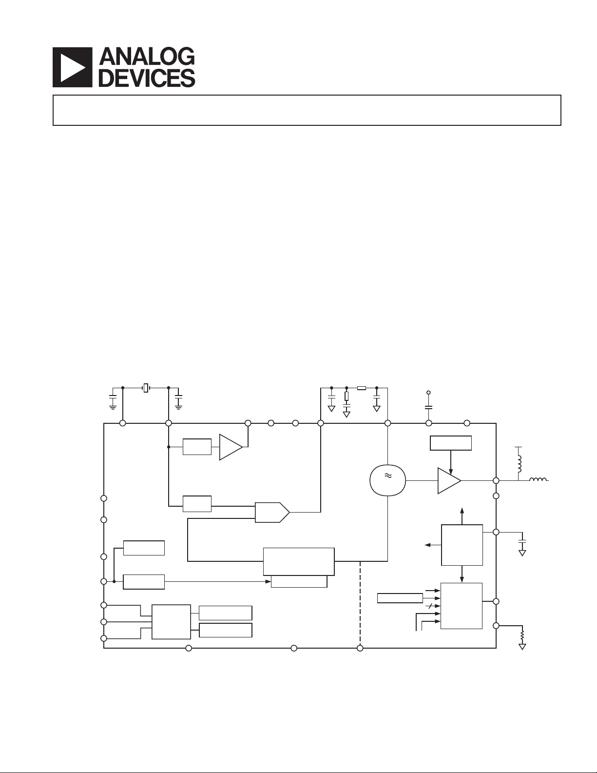
FUNCTIONAL BLOCK DIAGRAM
CPVDDCP
CLK
OSC1
OSC2
CLK
OUT
GENERAL DESCRIPTION
The ADF7011 is a low power OOK/ASK/FSK/GFSK UHF
transmitter designed for use in ISM band systems. It contains
and integrated VCO and Σ-∆ fractional-N PLL. The output
power, channel spacing, and output frequency are programmable with four 24-bit registers. The fractional-N PLL enables
the user to select any channel frequency within the European
433 MHz and 868 MHz bands, allowing the use of the ADF7011
in frequency hopping systems. The fractional-N also allows the
transmitter to operate in the less congested sub-bands of the
868 MHz to 870 MHz SRD band.
It is possible to choose from the four different modulation
schemes: Binary or Gaussian Frequency Shift Keying (FSK/
GFSK), Amplitude Shift Keying (ASK), or On/Off Keying
(OOK). The device also features a crystal compensation register
that can provide ±1 ppm resolution in the output frequency.
Indirect temperature compensation of the crystal can be accomplished inexpensively using this register.
Control of the four on-chip registers is via a simple 3-wire interface. The devices operate with a power supply ranging from
2.3 V to 3.6 V and can be powered down when not in use.
C
REG
VCO
GND
CP
OUT
VCO
C
VCO
IN
OOK/ASK
GND
V
DD
DV
D
GND
TxCLK
TxDATA
DATA
CLK
DD
OOK/ASK
FSK/GFSK
LE
SERIAL
INTERFACE
R
COMPENSATION
CE
FREQUENCY
CENTER
FREQUENCY
PFD/
CHARGE
PUMP
FRACTIONAL-N
SIGMA-DELTA
ADF7011
A
REV. 0
Information furnished by Analog Devices is believed to be accurate and
reliable. However, no responsibility is assumed by Analog Devices for its
use, nor for any infringements of patents or other rights of third parties that
may result from its use. No license is granted by implication or otherwise
under any patent or patent rights of Analog Devices. Trademarks and
registered trademarks are the property of their respective companies.
VCO
LOCK DETECT
GND
One Technology Way, P.O. Box 9106, Norwood, MA 02062-9106, U.S.A.
Tel: 781/329-4700 www.analog.com
Fax: 781/326-8703 © 2003 Analog Devices, Inc. All rights reserved.
TEST
PA
LDO
REGULATOR
MUXOUT
RF
RF
C
MUXOUT
R
OUT
GND
REG
SET
Page 2

ADF7011–SPECIFICATIONS
(VDD = 2.3 V to 3.6 V, GND = 0 V, TA = T
1
Typical specifications are at VDD = 3 V, TA = 25ⴗC, FPFD = 4 MHz @ 433 MHz,
MIN
to T
FPFD = 22.1184/5.)
Parameter Min Typ Max Unit
RF CHARACTERISTICS
Output Frequency Ranges
Lower SRD Band 433 435 MHz
Upper SRD Band 868 870 MHz
Phase Frequency Detector Frequency 3.4 20 MHz
TRANSMISSION PARAMETERS
Transmit Rate
2
FSK 0.3 76.8 kbits/s
ASK 0.3 9.6 kbits/s
GFSK 0.3 76.8 kbits/s
Frequency Shift Keying
FSK Separation
3
1 110 kHz using 3.625 MHz PFD
4.88 620 kHz using 20 MHz PFD
Gaussian Filter t 0.5
Amplitude Shift Keying Depth 28 dB
On/Off Keying 40 dB
Output Power (No Filtering)
4
868 MHz 3 dBm
433 MHz 10 dBm
Output Power Variation
Max Power Setting 9 12 dBm V
Max Power Setting 11 dBm V
Max Power Setting 9.5 dBm V
Programmable Step Size
–16 dBm to +12 dBm 0.3125 dB
LOGIC INPUTS
V
, Input High Voltage 0.7 V
INH
, Input Low Voltage 0.2 V
V
INL
I
C
, Input Current 1 µA
INH/IINL
, Input Capacitance 10 pF
IN
DD
DD
V
V
Control Clock Input 50 MHz
LOGIC OUTPUTS
VOH, Output High Voltage DV
, Output Low Voltage 0.4 V, I
V
OL
CLK
CLK
Rise/Fall Time 16 ns F
OUT
Mark: Space Ratio 50:50
OUT
– 0.4 V, I
DD
POWER SUPPLIES
Voltage Supply
DV
DD
2.3 3.6 V
Transmit Current Consumption
433 MHz
0 dBm (1 mW) 17 mA
10 dBm (10 mW) 29 mA
868 MHz
0 dBm (1 mW) 19 mA
3 dBm (2 mW) 20.5 mA
10 dBm (10 mW) 34 mA
Crystal Oscillator Block Current
Consumption 190 µA
Regulator Current Consumption 280 µA
Power-Down Mode
Low Power Sleep Mode 0.2 1 µA
, unless otherwise noted.
MAX
= 3.6 V
DD
= 3.0 V
DD
= 2.3 V
DD
= 500 µA
OH
= 500 µA
OL
= 4.8 MHz into 10 pF
CLK
REV. 0–2–
Page 3

ADF7011
Parameter Min Typ Max Unit
PHASE-LOCKED LOOP
VCO Gain 433 MHz/868 MHz 40/80 MHz/V @ 868 MHz
5
Phase Noise (In-Band)
Phase Noise (Out-of-Band)
Phase Noise (In-Band)7 868 MHz –83 dBc/Hz @ 5 kHz offset
Phase Noise (Out-of-Band)
Spurious
9, 10
47–74, 87.5–118, 174–230, 470–862 MHz –54 dBm
9 kHz – 1 GHz –36 dBm
Above 1 GHz –30 dBm. Assumes external harmonic filter.
Harmonics
10
Second Harmonic, 433 MHz/868 MHz –23/–28 –20/–23 dBc
Third Harmonic, 433 MHz/868 MHz –25/–29 –22/–25 dBc
Other Harmonics, 433 MHz/868 MHz –26/–40 –23/–35 dBc
REFERENCE INPUT
Crystal Reference
433 MHz 1.7 22.1184 MHz
868 MHz 3.4 22.1184 MHz
External Oscillator
Frequency 3.4 40 MHz
Input Level, High Voltage 0.7 V
Input Level, Low Voltage 0.2 V
FREQUENCY COMPENSATION
Pull In Range of Register 1 100 ppm
PA CHARACTERISTICS
RF Output Impedance
868 MHz 16 – j33 , Z
433 MHz 25 – j2.6 , Z
TIMING INFORMATION
Chip Enabled to Regulator Ready
Crystal Oscillator to CLK
4 MHz Crystal 1.8 ms
22.1184 MHz Crystal 2.2 ms
TEMPERATURE RANGE – T
NOTES
1
Operating temperature range is as follows: –40C to +85C.
2
Datarates should be limited to adhere to edge of band requirements in accordance with ETSI 300-220
3
Frequency Deviation = (PFD Frequency Mod Deviation )/212.
GFSK Frequency Deviation = (PFD Frequency 2m)/2
4
The output power is limited by the spurious requirements of ETSI at +55C. The addition of an output filter (see Applications section) will allow increased output
levels to >10 dBm at both 433 MHz and 868 MHz
5
VDD = 3 V, PFD = 4 MHz, PA = 10 dBm
6
VDD = 3 V, Loop Filter BW = 100 kHz
7
VDD = 3 V, PFD = 4.42368 MHz, PA = 3 dBm
8
VDD = 3 V, Loop Filter BW = 100 kHz
9
These spurious levels are based on a maximum output power of +3 dBm for 868 MHz and +10 dBm for 433 MHz. It assumes a PFD frequency of <5 MHz.
Recommended PFD frequencies are 4.42368 MHz (22.1184/5) for 868 MHz, and 4 MHz for 433 MHz operation. Compliance for higher output powers will require
an external filter. See Applications section.
10
Not production tested. Based on characterization.
Specifications subject to change without notice.
433 MHz –81 dBc/Hz @ 5 kHz offset
6
8
–90 dBc/Hz @ 1 MHz offset
–95 dBc/Hz @ 1 MHz offset
100 kHz loop BW
V
V
= 50
REF
= 50
REF
OUT
OK
A
DD
DD
10
50 200 µs
–40 +85 C
12
where m = Mod Control.
REV. 0
–3–
Page 4
ADF7011
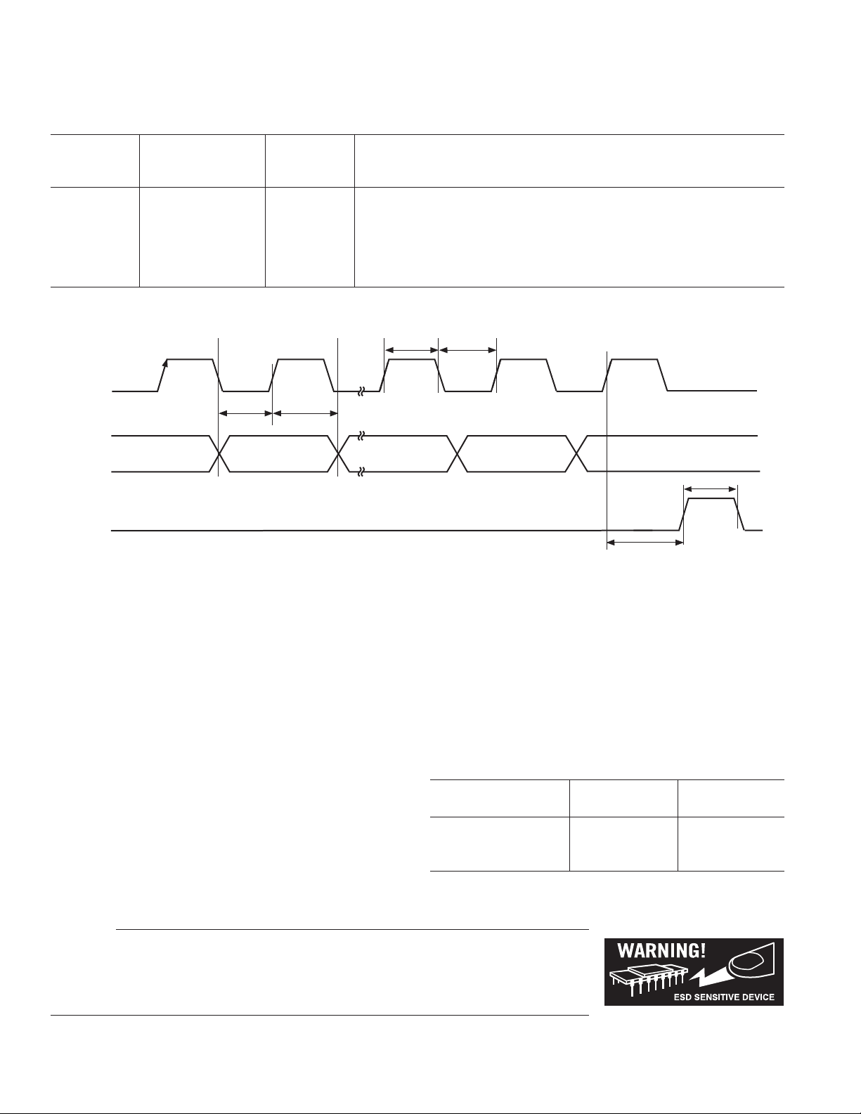
TIMING CHARACTERISTICS
(VDD = 3 V ⴞ 10%; VGND = 0 V, TA = 25ⴗC, unless otherwise noted.)
Limit at
to T
T
MIN
MAX
Parameter (B Version) Unit Test Conditions/Comments
t
1
t
2
t
3
t
4
t
5
t
6
Guaranteed by design but not production tested.
Specifications subject to change without notice.
CLOCK
DATA
LE
10 ns min DATA to CLOCK Setup Time
10 ns min DATA to CLOCK Hold Time
25 ns min CLOCK High Duration
25 ns min CLOCK Low Duration
10 ns min CLOCK to LE Setup Time
20 ns min LE Pulsewidth
t
1
DB23 (MSB) DB22 DB2
t
2
t
3
t
4
(CONTROL BIT C2)
DB1
DB0 (LSB)
(CONTROL BIT C1)
t
6
Figure 1. Timing Diagram
ABSOLUTE MAXIMUM RATINGS
(TA = 25°C, unless otherwise noted.)
1, 2
VDD to GND3 . . . . . . . . . . . . . . . . . . . . . . . . . –0.3 V to + 7 V
to GND . . . . . . . . . . . . . . . . . . . . . . . –0.3 V to + 7 V
CPV
DD
Digital I/O Voltage to GND . . . . . . . –0.3 V to DV
+ 0.3 V
DD
Operating Temperature Range
Industrial (B Version) . . . . . . . . . . . . . . . . –40°C to +85°C
Storage Temperature Range . . . . . . . . . . . . –65°C to +125°C
NOTES
1
Stresses above those listed under Absolute Maximum Ratings may cause permanent damage to the device. This is a stress rating only; functional operation of the
device at these or any other conditions above those listed in the operational
sections of this specification is not implied. Exposure to absolute maximum rating
conditions for extended periods may affect device reliability.
2
This device is a high performance RF integrated circuit with an ESD rating of
<1 kV and is ESD sensitive. Proper precautions should be taken for handling and
assembly.
3
GND = VCOGND = CPGND = RFGND = DGND = AGND = 0 V.
Maximum Junction Temperature . . . . . . . . . . . . . . . . . 125°C
TSSOP
Lead Temperature, Soldering
Vapor Phase (60 sec) . . . . . . . . . . . . . . . . . . . . . . . . . 235°C
Infrared (15 sec) . . . . . . . . . . . . . . . . . . . . . . . . . . . . 240°C
Thermal Impedance . . . . . . . . . . . . . . 150.4°C/W
JA
ORDERING GUIDE
Temperature
Model Range Package Option
ADF7011BRU –40ºC to +85ºC RU-24 (TSSOP)
ADF7011BRU-REEL –40ºC to +85ºC RU-24 (TSSOP)
ADF7011BRU-REEL7 –40ºC to +85ºC RU-24 (TSSOP)
CAUTION
ESD (electrostatic discharge) sensitive device. Electrostatic charges as high as 4000 V readily
accumulate on the human body and test equipment and can discharge without detection. Although the
ADF7011 features proprietary ESD protection circuitry, permanent damage may occur on devices
subjected to high energy electrostatic discharges. Therefore, proper ESD precautions are recommended
to avoid performance degradation or loss of functionality.
t
5
REV. 0–4–
Page 5
PIN CONFIGURATION
ADF7011
R
SET
CPV
CP
GND
CP
OUT
DATA
CLK
TxDATA
TxCLK
MUXOUT
D
GND
DD
CE
LE
1
2
3
4
5
ADF7011
6
TOP VIEW
(Not to Scale)
7
8
9
10
11
12
TSSOP
24
C
REG
23
C
VCO
22
VCO
IN
21
A
GND
20
RF
OUT
19
RF
GND
18
DV
DD
17
TEST
16
VCO
GND
15
OSC1
14
OSC2
13
CLK
OUT
PIN FUNCTION DESCRIPTIONS
Pin No. Mnemonic Function
1R
2 CPV
SET
DD
External Resistor to Set Change Pump Current and Some Internal Bias Currents. Use 4.7 kΩ as default:
I
CP MAX
So, with R
Charge Pump Supply. This should be biased at the same level as RF
95.
=
R
SET
= 4.7 kΩ, I
SET
CP MAX
= 2.02 mA.
and DVDD. The pin should be
OUT
decoupled with a 0.1 µF capacitor as close to the pin as possible.
3CP
4CP
GND
OUT
Charge Pump Ground.
Charge Pump Output. This output generates current pulses that are integrated in the loop filter. The
integrated current changes the control voltage on the input to the VCO.
5CEChip Enable. A logic low applied to this pin powers down the part. This must be high for the part to
function. This is the only way to power down the regulator circuit.
6 DATA Serial Data Input. The serial data is loaded MSB first with the two LSBs being the control bits. This is a
high impedance CMOS input.
7 CLK Serial Clock Input. This serial clock is used to clock in the serial data to the registers. The data is latched
into the 24-bit shift register on the CLK rising edge. This input is a high impedance CMOS input.
8LELoad Enable, CMOS Input. When LE goes high, the data stored in the shift registers is loaded into one
of the four latches, the latch being selected using the control bits.
9 TxDATA Digital data to be transmitted is input on this pin.
10 TxCLK GFSK Only. This clock output is used to synchronize microcontroller data to the TxDATA pin of the
ADF7011. The clock is provided at the same frequency as the data rate.
11 MUXOUT This multiplexer output allows either the digital lock detect (most common), the scaled RF, or the scaled
reference frequency to be accessed externally. Used commonly for system debug. See the Function Register Map.
12 D
GND
13 CLK
OUT
Ground Pin for the RF Digital Circuitry.
The Divided Down Crystal Reference with 50:50 Mark-Space Ratio. May be used to drive the clock
input of a microcontroller. To reduce spurious components in the output spectrum, the sharp edges can
be reduced with a series RC. For 4.8 MHz output clock, a series 50 Ω into 10 pF will reduce spurs to
< –50 dBc. Defaults on power-up to divide by 16.
14 OSC2 Oscillator Pin. If a single-ended reference (such as a TCXO) is used, it should be applied to this pin.
When using an external signal generator, a 51 Ω resistor should be tied from this pin to ground. The
XOE bit in the R register should set high when using an external reference.
REV. 0
–5–
Page 6

ADF7011
PIN FUNCTION DESCRIPTIONS (continued)
Pin No. Mnemonic Function
15 OSC1 Oscillator Pin. For use with crystal reference only. This is three-stated when an external reference oscilla-
tor is used.
16 VCO
GND
17 TEST Input to the RF Fractional-N Divider. This pin allows the user to connect an external VCO to the part.
18 DV
19 RF
20 RF
21 A
22 VCO
23 C
24 C
DD
GND
OUT
GND
IN
VCO
REG
Voltage Controlled Oscillator Ground.
Disabling the internal VCO activates this pin. If the internal VCO is used, this pin should be grounded.
Positive Supply for the Digital Circuitry. This must be between 2.3 V and 3.6 V. Decoupling capacitors
to the analog ground plane should be placed as close as possible to this pin.
Ground for Output Stage of Transmitter.
The modulated signal is available at this pin. Output power levels are from –16 dBm to +12 dBm. The
output should be impedance matched to the desired load using suitable components. See the RF Output
Stage section.
Ground Pin for the RF Analog Circuitry.
The tuning voltage on this pin determines the output frequency of the Voltage Controlled Oscillator
(VCO). The higher the tuning voltage, the higher the output frequency.
A 0.22 µF capacitor should be added to reduce noise on VCO bias lines. Tied to the C
A 2.2 µF capacitor should be added at C
, tied to GND, to reduce regulator noise and improve
REG
REG
pin.
stability. A reduced capacitor will improve regulator power-on time but may cause higher spurious
components.
REV. 0–6–
Page 7
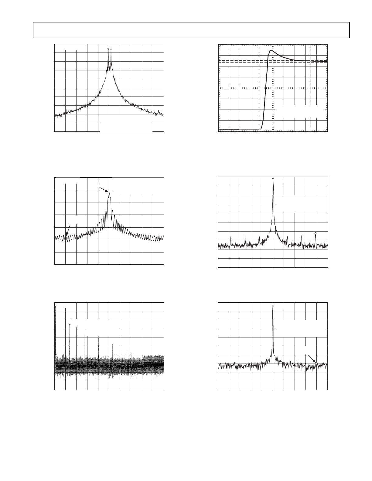
Typical Performance Characteristics–ADF7011
RL = 10.0dBm
VDD = 3V
PFD FREQUENCY = 19.2MHz
LOOP BW = 100kHz
868.3MHz SPAN 5.000MHz
TPC 1. FSK Modulated Signal, F
RBW = 1kHz
DEVIATION
Data Rate = 19.2 kbps, 10 dBm
RL = 10.0dBm
–36dBm
@ 200kHz
–2dBm
VDD = 3V
PFD FREQUENCY = 19.2MHz
LOOP BW = 1MHz
RBW = 3kHz
= 58 kHz,
885.000MHz
868.000MHz
VDD = 3V
PFD FREQUENCY = 19.2MHz
LOOP BW = 100kHz
851.000MHz
5.00s–20.00s
5.00s/DIV
30.00s
TPC 4. PLL Settling Time, 852 MHz to 878 MHz,
23 s (±400 kHz)
+10dBm
VDD = 3V
PFD FREQUENCY = 19.2MHz
LOOP BW = 100kHz
RBW = 100kHz
+19.2MHz
–61dBc
868.3MHz SPAN 500kHz
TPC 2. OOK Modulated Signal, Data Rate = 4.8 kbps,
4 dBm
+10dBm
SECOND HARMONIC
–22dBc
THIRD HARMONIC
–34dBc
START 800MHz STOP 7.750GHz
RBW 1.0MHz
TPC 3. Harmonic Levels at 10 dBm Output Power.
See Figure 15.
RBW 100kHz SPAN 50.00MHz868.3MHz
TPC 5. PFD Spurious/Fractional Spurious Components
+10dBm
VDD = 3V
PFD FREQUENCY = 19.2MHz
LOOP BW = 100kHz
RBW = 30Hz
PN @ 4kHz
80dBc/Hz
SPAN 10.00kHz868.3MHz
TPC 6. In-Band Phase Noise
REV. 0
–7–
Page 8
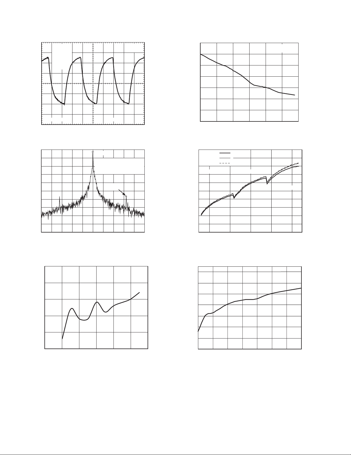
ADF7011
C1 RISE
144.8ns
C1 FALL
145.6ns
C1 +DUTY
49.385%
Ch1 500mV
TPC 7. 1.6 MHz CLOCK
C1 FREQ
1.6MHz
M 200ns
Waveform
OUT
+10dBm
VDD = 3V
PFD FREQUENCY = 19.2MHz
LOOP BW = 100kHz
RBW = 10Hz
+1.6MHz
–53dBc
SPAN 5.00MHz868.3MHz
110
100
90
80
70
GAIN (MHz/V)
60
50
40
885
20
VDD = 2.2V
15
VDD = 3.0V
VDD = 3.6V
10
5
0
–5
–10
LEVEL (dBm)
–15
–20
–25
–30
40
FREQUENCY (MHz)
TPC 10. Typical VCO Gain
MID RANGELOW RANGE
60 80 100 120
PA SETTING (Modulation Register)
VDD = 3V
= 25C
T
A
935
HIGH RANGE
945925915905895
TPC 8. Spurious Signal Generated by CLOCK
0
–5
–10
–15
SENSITIVITY (dBm)
–20
–25
0.8 0.9 1.0 1.1 1.2 1.3 1.4
FREQUENCY (GHz)
TPC 9. N-Divider Input Sensitivity
OUT
TPC 11. PA Output Programmability, TA = 25°C
44
42
40
38
36
CURRENT (mA)
34
32
30
2.2
SUPPLY VOLTAGE (V)
3.43.02.82.62.4
3.2 3.6
TPC 12. IDD vs. VDD @ 10 dBm
REV. 0–8–
Page 9

REGISTER MAPS
ADF7011
RF R REGISTER
RESERVED
LD
PRECISION
DB22
DB23
PRE-
SCALER
DB22
DB23
P1
CL4
VCO
BAND
DB21
N8
INDEX
COUNTER
DB21
CLK
OUT
DB19 DB17 DB16 DB15 DB14 DB13 DB12 DB11 DB10 DB9 DB8 DB7 DB6 DB5 DB4 DB3 DB2
DB18DB20DB21DB22DB23
XOE
4-BIT R-VALUE
R1
11-BIT FREQUENCY ERROR CORRECTION
RF N REGISTER
DB20
8-BIT INTEGER-N
DB19
DB18
DB17
DB16
DB15
DB14
DB13
M12
DB12
DB11
12-BIT FRACTIONAL-N
DB10
DB9
DB8
DB7
DB6
DB5
DB4
MODULATION REGISTER
GFSK MOD
CONT ROL
DB20
DB19
DB18
MODULATION DEVIATION
DB17
DB16
DB15
DB14
DB13
DB12
DB11
D1D2D3D4D5D6D7MC1MC2MC3IC1IC2
DB10
P7
POWER AMPLIFIER
DB8
DB9
P5
P6
DB7
DB6
DB5
DB4
F1
F2F3F4F5F6F7F8F9F10F11R2R3R4X1CL1CL2CL3R1R2
DB3
DB2
M1
M2M3M4M5M6M7M8M9M10M11N1N2N3N4N5N6N7V1LDP
MODULATION
SCHEME
DB3
DB2
S1S2P1P2P3P4
CONTROL
BITS
DB1 DB0
C2 (0)
CONTROL
BITS
DB1
C2 (0)
CONTROL
BITS
DB1
C2 (1)
C1 (0)
DB0
C1 (1)
DB0
C1 (0)
REV. 0
DB23
DB22 DB21 DB20
TEST MODES
DB19
DB18
DB17
DB16
DB15
FUNCTION REGISTER
MUXO UT
DB14
DB13 DB12 DB11
M2
–9–
M1
VCO
DB10
FAST LOCK
DISABLE
DB9
DB8 DB7 DB6 DB5
CP3CP4VP1M3M4T1T2T3T4T5T6T7T8T9
CHARGE
PUMP
CP1CP2
I1
DATA
INVERT
CLK
DB4
PD3
OUT
ENABLE
DB3
PD2
PA
ENABLE
DB2
PD1
PLL
ENABLE
CONTROL
BITS
DB1
C2 (1)
DB0
C1 (1)
Page 10

ADF7011
RF R Register
RESERVED
DB23 DB22
DB21
CL4
CLK
OUT
DB20 DB19
4-BIT R-VALUE
XOE
DB17
DB18
X1
XOE
DB16
DB15
DB14 DB13 DB12
0 XTAL OSCILLATOR ON
1 XTAL OSCILLATOR OFF
DB2
F1
CONTROL
DB1
C2 (0)
F1F2F3F11
15
BITS
DB0
C1 (0)
F-COUNTER
OFFSET
11-BIT FREQUENCY ERROR CORRECTION
DB11
DB10
R1
.........................................................................................................................................................
e.g., F-COUNTER OFFSET = 1, FRACTIONAL OFFSET = 1/2
DB8
DB9
0 ........... 1 1 1 1023
0 ........... 1 1 0 1022
0 ........... . . . .
0 ........... 0 0 1 1
0 ........... 0 0 0 0
1 ........... 1 1 1 1
1 ........... 1 1 0 2
1 ........... 0 0 1 1023
1 ........... 0 0 0 1024
DB7 DB6
...........
........... . . . .
DB5 DB4
DB3
F2F3F4F5F6F7F8F9F10F11R2R3R4X1CL1CL2CL3R1R2
CLK
CL4
0 001 2
0 010 4
0 011 6
0 100 8
. ... .
. ... .
. ... .
1 100 24
1 101 26
1 110 28
1 111 30
CL3
CL2
CL1
OUT
DIVIDE RATIO
R4 R3
0 0 0 1 1
0 0 1 0 2
0 0 1 1 3
0 1 0 0 4
. . . . .
. . . . .
. . . . .
1 1 0 0 12
1 1 0 1 13
1 1 1 0 14
1 1 1 1 15
R2
R1
RF R COUNTER
DIVIDE RATIO
REV. 0–10–
Page 11

RF N Register
ADF7011
LD
DB23
VCO
PRECISION
DB22
BAND
DB21
DB2
M1
CONTROL
BITS
DB1
C2 (0)
DB0
C1 (1)
8-BIT INTEGER-N
DB19
DB20
N8
N8 N7 N6 N5 N4 N3 N2 N1
0 0011111 31
0 0100000 32
0 0100001 33
0 0100010 34
. ....... .
. ....... .
. ....... .
1 1111101 253
1 1111110 254
1 1111111 255
DB17
DB18
M12 M11 M10 .......... M3 M2 M1
0 0 0 .......... 1 0 0 4
0 0 0 .......... 1 0 1 5
0 0 0 .......... 1 1 0 6
. . . .......... ... .
. . . .......... ... .
. . . .......... ... .
1 1 1 .......... 1 0 0 4092
1 1 1 .......... 1 0 1 4093
1 1 1 .......... 1 1 0 4094
1 1 1 .......... 1 1 1 4095
DB15
DB16
MODULUS
DB14
DB13
M12
DB12
DB11
12-BIT FRACTIONAL-N
DB6
DB10
e.g., MODULUS DIVIDE RATIO = 2048 –> FRACTION 1/2
DB8
DB9
e.g., SETTING F = 0 IN FSK MODE TURNS ON THE
- WHILE THE PLL IS AN INTEGER VALUE
DB7
DB5 DB4
DIVIDE RATIO
N COUNTER
DIVIDE RATIO
DB3
M2M3M4M5M6M7M8M9M10M11N1N2N3N4N5N6N7V1LDP
REV. 0
VCO BAND
V1
(MHz)
0 866–870
1 433–435
LOCK DETECT
LDP
PRECISION
0 3 CYCLES < 15ns
1 5 CYCLES < 15ns
–11–
THE N VALUE CHOSEN IS A MINIMUM OF
2
P
+ 3P + 3. FOR PRESCALER = 8/9, THIS
MEANS A MINIMUM N DIVIDE OF 91.
Page 12

ADF7011
Modulation Register
INDEX
COUNTER
PRE-
SCALER
DB22DB23
P1 P5P6P7 S1
P1 RF PRESCALER
0 4/5
1 8/9
GFSK MOD
CONTROL
IF AMPLITUDE SHIFT KEYING SELECTED, TxDATA = 0
D7 D6 . D2 D1
00.X XPA OFF
01.0 016.0dBm
01.0 1161(10/32)
.... ..
01.1 11631(10/32)
10.0 06dBm
10.0 161(10/32)
.... ..
10.1 161(10/32)
11.0 02dBm
11.0 121(10/32)
11.. ..
11.1 112dBm
MODULATION DEVIATION
DB16 DB15 DB14DB17DB20 DB19 DB18DB21
DB13 DB12 DB11 DB10 DB9 DB8 DB7 DB6 DB5 DB4 DB3 DB2 DB1 DB0
POWER AMPLIFIER
SCHEME
0 0 FSK
0 1 GFSK
1 0 ASK
1 1 OOK
POWER AMPLIFIER OUTPUT LEVEL
P7 P6 . P2 P1
00. X XPA OFF
01. 0 016.0dBm
01. 0 1161(10/32)
.... ..
01. 1 11631(10/32)
10. 0 06dBm
10. 0 161(10/32)
.... ..
10. 1 161(10/32)
11. 0 02dBm
11. 0 121(10/32)
11. . ..
11. 1 112dBm
MODU LATION
SCHEM
S2P1P2P3P4D1D2D3D4D5D6D7MC1MC2MC3IC1IC2
S2 S1
CONTROL
E
BITS
C2 (1) C1 (0)
MODULATION
IF FREQUENCY SHIFT KEYING SELECTED
D7. . . . D3 D2 D1 F DEVIATION
0 . . . . 0 0 0 PLL MODE
0 . . . . 0 0 1 1 F
0 . . . . 0 1 0 2 F
0 . . . . 0 1 1 3 F
. . . . ...............
1 . . . . 1 1 1 127 F
IF GAUSSIAN FREQUENCY SHIFT KEYING SELECTED
INDEX
IC2 IC1
COUNTER
0 0 16
0 1 32
1 0 64
1 1 128
MC3 MC2 MC1
0 0 0 0
0 0 1 1
. . . .
1 1 1 7
GFSK MOD
CONTROL
F
= F
STEP
PFD
STEP
STEP
STEP
STEP
D7 D3 D2 D1 DIVIDER FACTOR
00 0 00
00 0 11
00 1 02
00 1 1 3
.. ........
11 1 1127
12
/2
REV. 0–12–
Page 13

Function Register
ADF7011
TEST MODES
DB19 DB18 DB17 DB16 DB14 DB13 DB12 DB11 DB10 DB9 DB8 DB7 DB6 DB5 DB4 DB3 DB2 DB1 DB0DB20DB21DB23 DB22
T6T7T8T9
MUXOUT
DB15
T2T3T4T5 T1 M2M3M4 M1 VP1 CP4 C2CP3 C1 PD3 I1 PD2 PD1
VP1 VCO DISABLE
0 VCO ON
1 VCO OFF
CP4 CP FLOCK DOWN
0 BLEED OFF
1 BLEED ON
CP3 CP FLOCK UP
0 BLEED OFF
1 BLEED ON
CP2 CP1 ICP (mA)
0 0 0.50 0.29 0.14
0 1 1.50 0.87 0.41
1 0 2.51 1.44 0.68
1 1 3.51 2.02 0.95
R
SET
2.7k 4.7k 10k
VCO
DISABLE
FAST LOCK
CHARGE
PUMP
I1 DATA INVERT
0 DATA
1 DATA
DATA
INVERT
OUT
CLK
ENABLEPAENABLE
PLL
PD1 PLL ENABLE
0 PLL OFF
1 PLL ON
PD2 PA ENABLE
0 PA OFF
1 PA ON
ENABLE
CONTROL
BITS
C2 (1)
C1 (1)
M4 M3 M2 M1 MUXOUT
0 0 0 0 LOGIC LOW
0 0 0 1 LOGIC HIGH
0 0 1 0 THREE-STATE
0 0 1 1 REGULATOR READY (DEFAULT)
0 1 0 0 DIGITAL LOCK DETECT
0 1 0 1 ANALOG LOCK DETECT
0 1 1 0 R DIVIDER / 2 OUTPUT
0 1 1 1 N DIVIDER / 2 OUTPUT
1 0 0 0 RF R DIVIDER OUTPUT
1 0 0 1 RF N DIVIDER OUTPUT
1 0 1 0 DATA RATE
1 0 1 1 LOGIC LOW
1 1 0 0 LOGIC LOW
1 1 0 1 LOGIC LOW
1 1 1 0 NORMAL TEST MODES
1 1 1 1 - TEST MODES
PD3 CLK
0CLK
1CLK
OUT
OUT
OUT
ENABLE
OFF
ON
REV. 0
–13–
Page 14

ADF7011
Default Values for Registers
R REGISTER
RESERVED
DB23 DB22
LD
PRECI SION
DB23
DB22
PRE-
SCALER
DB23
1
DB21
VCO
BAND
DB21
1
INDEX
COUNTER
DB22
1
DB21
CLK
DB20 DB19
DB19
DB20
GFSK MOD
CONTROL
DB20
OUT
DB18 DB17 DB16 DB15 DB14 DB13 DB12 DB11
8-BIT INTEGER-N
DB18
DB17
XOE
DB16
4-BIT R-VALUE
DB15
DB14
1
DB13
1
MODULATION REGISTER
MODULATION DEVIATION
DB19
DB18
DB17
DB16
DB15
DB14
DB13
N REGISTER
DB12
DB11
DB11
DB12
000000000000
11-BIT FREQUENCY ERROR CORRECTION
DB10 DB9 DB8
12-BIT FRACTIONAL-N
DB10
DB9
DB8
POWER AMPLIFIER
DB9
DB8
1
DB10
1
DB7 DB6
DB7
DB7
0
DB5 DB4 DB3 DB2
DB6
DB5 DB4
DB6
DB5
0000000000000000000
DB3
MODULATION
SCHEME
DB4 DB3
CONTROL
BITS
DB1
DB0
C1 (0)
C2 (0)
0
CONTROL
BITS
DB0
DB1
DB2
0000000000000000000
0
DB2
0
00000
C2 (0)
CONTROL
BITS
DB1
C2 (1)
C1 (1)
DB0
C1 (0)
DB23
DB22 DB21 DB20
TEST MODES
DB19
DB18
DB17
DB16
DB15
FUNCTION REGISTER
MUXO UT
DB14
DB13 DB12 DB11
1
DB2
PLL
0
ENABLE
CONTROL
BITS
DB1
C2 (1)
DB0
C1 (1)
FAST LOCK
VCO
DISABLE
DB10
DB9
1
CHARGE
PUMP
DB8 DB7 DB6 DB5
00000000000000
11
DATA
0
INVERT
CLK
DB4
OUT
1
ENABLE
DB3
PA
ENABLE
0
REV. 0–14–
Page 15

ADF7011
CIRCUIT DESCRIPTION
Reference Input Section
The on-board crystal oscillator circuitry (Figure 2), allows the
use of an inexpensive quartz crystal as the PLL reference. The
oscillator circuit is enabled by setting XOE low. It is enabled by
default on power-up and is disabled by bringing CE low. Two
parallel resonant capacitors are required for oscillation at the
correct frequency; the value of these is dependant on the crystal
specification. Errors in the crystal can be corrected using the
error correction register within the R register. A single-ended
reference (TCXO, CXO) may be used. The CMOS levels should
be applied to OSC2, with XOE set high.
10pF
10pF
OSC2
OSC1
500k
100k
NC
SW1
XTAL OSCILLATOR
DISABLED
100k
BUFFER
TO R COUNTER AND
CLK
OUT
DIVIDE
Figure 2. Oscillator Circuit on the ADF7011
CLK
The CLK
Divider and Buffer
OUT
circuit takes the reference clock signal from the
OUT
oscillator section above and supplies a divided down 50:50 markspace signal to the CLK
pin. An even divide from 2 to 30 is
OUT
available. This divide is set by the four MSBs in the R register.
On power-up, the CLK
defaults to divide by 16.
OUT
DV
DD
ENABLE BIT
CLK
OUT
Prescaler, Phase Frequency Detector (PFD), and Charge Pump
The dual-modulus prescaler (P/P + 1) divides the RF signal
from the VCO to a lower frequency that is manageable by the
CMOS counters.
The PFD takes inputs from the R Counter and the N Counter
(N = Int + Fraction) and produces an output proportional to the
phase and frequency difference between them. Figure 4 is a
simplified schematic.
V
P
CHARGE
PUMP
CP
GND
R DIVIDER
N DIVIDER
CP OUTPUT
R DIVIDER
N DIVIDER
HI D1 Q1
U1
CLR1
CLR2
HI D2 Q2
U2
UP
DELAY
ELEMENT
DOWN
U3
CP
OSC1
DIVIDER
1 TO 15
The output buffer to CLK
DIVIDE
BY 2
Figure 3. CLK
is enabled by setting Bit DB4 in
OUT
OUT
Stage
CLK
OUT
the function register high. On power-up, this bit is set high.
The output buffer can drive up to a 20 pF load with a 10% rise
time at 4.8 MHz. Faster edges can result in some spurious
feedthrough to the output. A small series resistor (50 Ω) can be
used to slow the clock edges to reduce these spurs at F
CLK
.
R Counter
The 4-bit R Counter divides the reference input frequency by
an integer from 1 to 15. The divided down signal is presented
as the reference clock to the phase frequency detector (PFD).
The divide ratio is set in the R register. Maximizing the PFD
frequency reduces the N value. Having a higher PFD will
result in a higher level of spurious components. A PFD of
close to 4 MHz is recommended. This reduces the noise multiplied at a rate of 20 log(N) to the output, as well as reduces
occurrences of spurious components. The R register defaults
to R = 1 on power-up.
Figure 4. PFD Stage
The PFD includes a delay element that sets the width of the
antibacklash pulse. The typical value for this in the ADF7011 is
3 ns. This pulse ensures that there is no dead zone in the PFD
transfer function and minimizes phase noise and reference spurs.
MUXOUT and Lock Detect
The MUXOUT pin allows the user to access various internal
points in the ADF7011. The state of MUXOUT is controlled
by Bits M1 to M4 in the function register.
Regulator Ready
This is the default setting on MUXOUT after the transmitter
has been powered up. The power-up time of the regulator is
typically 50 µs. Since the serial interface is powered from the
regulator, it is necessary for the regulator to be at its nominal
voltage before the ADF7011 can be programmed. The status
of the regulator can be monitored at MUXOUT. Once the
Regulator Ready signal on MUXOUT is high, programming of
the ADF7011 may begin.
REV. 0
–15–
Page 16

ADF7011
REGULATOR READY
DIGITAL LOCK DETECT
ANALOG LOCK DETECT
R COUNTER/2 OUTPUT
N COUNTER/2 OUTPUT
R COUNTER OUTPUT
N COUNTER OUTPUT
MUX CONTROL
Figure 5. MUXOUT Stage
DV
DD
DGND
MUXOUT
Digital Lock Detect
Digital lock detect is active high. The lock detect circuit is contained at the PFD. When the phase error on five consecutive
cycles is less than 15 ns, lock detect is set high. Lock detect
remains high until 25 ns phase error is detected at the PFD.
Since no external components are needed for digital lock detect,
it is more widely used than analog lock detect.
Analog Lock Detect
This N-channel open-drain lock detect should be operated with
an external pull-up resistor of 10 kΩ nominal. When lock has been
detected, this output will be high with narrow low-going pulses.
Voltage Regulator
The ADF7011 requires a stable voltage source for the VCO and
modulation blocks. The on-board regulator provides 2.2 V
using a band gap reference. A 2.2 µF capacitor from C
REG
to
ground is used to improve stability of the regulator over a supply ranging from 2.3 V to 3.6 V. The regulator consumes less
than 400 µA and can only be powered down using the chip
enable (CE) pin. Bringing CE low disables the regulator and
also erases all values held in the registers. The serial interface
operates off the regulator supply; therefore, to write to the part,
the user must have CE high. Regulator status can be monitored
using the Regulator Ready signal from MUXOUT.
Loop Filter
The loop filter integrates the current pulses from the charge
pump to form a voltage that tunes the output of the VCO to the
desired frequency. It also attenuates spurious levels generated
by the PLL. A typical loop filter design is shown in Figure 6.
CHARGE
PUMP OUT
VCO
Figure 6. Typical Loop Filter Configuration––Third
Order Integrator
In FSK, the loop should be designed so that the loop bandwidth
(LBW) is approximately five times the data rate. Widening
the LBW excessively reduces the time spent jumping between
frequencies but may cause insufficient spurious attenuation.
For ASK systems, the wider the loop BW the better. The sudden large transition between two power levels will result in VCO
pulling and can cause a wider output spectrum than is desired.
By widening the loop BW to >10 times the data rate, the amount
of the VCO pulling is reduced since the loop will quickly settle
back to the correct frequency. The wider LBW may restrict the
output power and data rate of ASK based systems, compared
with FSK based systems.
Narrow-loop bandwidths may result in the loop taking long
periods of time to attain lock. Careful design of the loop filter is
critical in obtaining accurate FSK/GFSK modulation.
For GFSK, it is recommended that an LBW of 2.0 to 2.5 times
the data rate be used to ensure sufficient samples are taken of
the input data while filtering system noise.
REV. 0–16–
Page 17

ADF7011
Voltage Controlled Oscillator (VCO)
An on-chip VCO is included on the transmitter. The VCO converts the control voltage generated by the loop filter into an output
frequency that is sent to the antenna via the power amplifier
(PA). The VCO has a typical gain of 80 MHz/V and operates
from 866 MHz to 870 MHz. The PD1 bit in the function register is the active high bit that turns on the VCO. A frequency
divided by 2 is included to allow operation in the lower 450 MHz
band. To enable operation in the lower band, the V1 bit in the
N Register should be set to 1.
The VCO needs an external 220 nF between the VCO and the
regulator to reduce internal noise.
VCO CONTROL BIT
TO PA AND
N DIVIDER
LOOP FILTER
C
REG
220nF
PIN
VCO
DIVIDE
BY 2
VCO SELECT BIT
MUX
Figure 7. Voltage Controlled Oscillator
RF Output Stage
The RF output stage consists of a DAC with a number of current sources to adjust the output power level. To set up the
power level
• FSK GFSK: The output power is set using the modulation
Register by entering a 7-bit number into Bits P1–P7. The
two MSBs set the range of the output stage, while the five
LSBs set the output power in the selected range.
• ASK: The output power as set up for FSK is the output
power for a TxDATA of 1. The output power for a zero
data bit is set up the same way but using Bits D1–D7.
The output stage is powered down by setting Bit PD2 in the
function register to zero.
LOW
MED
HIGH
P5 P1 P7, P6
Figure 8. Output Stage
Serial Interface
The serial interface allows the user to program the four 24-bit
registers using a 3-wire interface (CLK, Data, and Load Enable).
The serial interface consists of a level shifter, a 24-bit shift register, and four latches. Signals should be CMOS compatible. The
serial interface is powered by the regulator, and therefore is
inactive when CE is low.
Table I. C2, C1 Truth Table
C2 C1 Data Latch
00 R Register
01 N Register
10 Modulation Register
11 Function Register
Data is clocked into the shift register, MSB first, on the rising
edge of each clock (CLK). Data is transferred to one of four
latches on the rising edge of LE. The destination latch is determined by the value of the two control bits (C2 and C1). These
are the two LSBs, DB1 and DB0, as shown in the timing diagram of Figure 1.
V
DD
L1
PA
RF
OUT
C1
L2
50
REV. 0
Figure 9. Output Stage Matching
–17–
Page 18

ADF7011
0.00
0.20 0.50 1.00
0.0
150
140
0.20
130
120
25 – j2.6
433MHz
0.50
110
16 – j33
868MHz
100
1.00
90
80
70
Figure 10. Output Impedance on Smith Chart
Fractional-N
N Counter and Error Correction
The ADF7011 consists of a 15-bit - fractional-N divider.
The N Counter divides the output frequency to the output
stage back to the PFD frequency. It consists of a prescaler,
integer, and fractional part.
The prescaler can be 4/5 or 8/9. A prescaler setting of 8/9 is
recommended for 868 MHz operation. A prescaler setting of
4/5 is recommended for 433 MHz operation.
The output frequency of the PLL is
PFD Frequency Int
REFERENCE IN
R
PFD/
CHARGE
PUMP
FRACTIONAL-N
×+
Fractional Error
×
8
()
THIRD ORDER
- MODULATOR
Figure 11. Fractional-N PLL
Fractional-N Registers
The fractional part is made up of a 15-bit divide, made up of a
12-bit N value in the N register summed with a 10-bit value
(plus sign bit) in the R register that is used for error correction,
as shown in Figure 12.
2.00
2.00
60
15
2
5.00
5.00
40
50
+
VCO
N
INTEGER-N
30
The resolution of each register is the smallest amount that the
output frequency can be changed by changing the LSB of the
register.
Changing the Output Frequency
The fractional part of the N register changes the output frequency by
PFD Frequency Fractional gister Value× Re
12
2
The frequency error correction contained in the R register
changes the output frequency by
PFD Frequency Error Correction gisterValue× Re
15
2
By default, this will be set to 0. The user can calibrate the system
and set this by writing a twos complement number to Bits F1–F11
in the R register. This can be used to compensate for initial error,
temperature drift, and aging effects in the crystal reference.
Integer-N Register
The integer part of the N Counter contains the prescaler and A
and B Counters. It is eight bits wide and offers a divide of
2
+ 3P + 3 to 255.
P
The combination of the integer (255) and the fractional (31767/
31768) gives a maximum N Divider of 256. The minimum
usable PFD is
Maximum quired Output FrequencyRe
255 1+
()
For use in the European 868 MHz to 870 MHz band, there is a
restriction to using a minimum PFD of 3.4 MHz to allow the
user to have a center frequency of 870 MHz.
PFD Frequency
The PFD frequency is the number of times a comparison is
made between the reference frequency and the feedback signal
from the output.
The higher the PFD frequency, the more often a comparison is
made at the PFD. This means that the frequency lock time will
be reduced when jumping from one frequency to another by
increasing the PFD. Having a PFD of > 5 MHz will reduce the
available output power due to EN300-220 spurious regulations.
M12 M11 M10 M9 M8 M7M6M5M4M3M2M1
12-BIT N VALUE
F10 F9 F8 F7F6 F5F4
10-BIT ( SIGN) ERROR CORRECTION
N14 N13 N12 N11 N10 N9 N8 N7 N6 N5 N4 N3
15-BIT FRACTIONAL N REGISTER
Figure 12. Fractional Components
F3 F2 F1
N2 N1 N0
REV. 0–18–
Page 19

ADF7011
MODULATION SCHEMES
Frequency Shift Keying (FSK)
Frequency shift keying is implemented by setting the N value
for the center frequency and then toggling this with the TxDATA
line. The deviation from the center frequency is set using Bits
D1–D7 in the modulation register. The deviation from the
center frequency in Hz is
FSK Hz
DEVIATION
()
PFD Frequency Modulation Number
=
×
12
2
The modulation number is a number from 1 to 127 (Bits D1–
D7 in modulation register). FSK is selected by setting Bits S1
and S2 to zero in the modulation register.
CHEAP AT CRYSTAL
FSK DEVIATION
FREQUENCY
–F
DEV
+F
DEV
TxDATA
ⴜR
FRACTIONAL-N
INTERNAL VCO USING
SPIRAL INDUCTORS
GAIN 70 MHz/V–90 MHz/V
PFD/
CHARGE
PUMP
THIRD ORDER
⌺-⌬
MODULATOR
INTEGER-N
VCO
PA STAGE
Figure 13. FSK Implementation
Gaussian Frequency Shift Keying (GFSK)
Gaussian frequency shift keying reduces the bandwidth occupied
by the transmitted spectrum by digitally prefiltering the TxDATA.
A TxCLK output line is provided from the ADF7011 for synchronization of TxDATA from the microcontroller. The TxCLK
line may be connected to the clock input of an external shift
register that clocks data to the transmitter at exact data rate.
DATA FROM
MICROCONTROLLER
SHIFT
REGISTER
TxDATA
ADF7011
TxCLK
ANTENNA
Figure 14. TxCLK Pin Synchronizing Data for GFSK
Setting Up the ADF7011 for GFSK
To set up the frequency deviation, set the PFD and the mod
control Bits MC1 to MC3.
GFSK Hz
DEVIATION
()
PFD Frequency
=
2
12
× 2
m
where m is mod control (Bits MC1 to MC3 in the modulation
register).
To set up the GFSK data rate
Data Rate bits s
()
/
=
Divider Factor Index Counter
PFD Frequency
×
Amplitude Shift Keying (ASK)
Amplitude shift keying is implemented by switching the output
stage between two discrete power levels. This is implemented by
toggling the DAC, which controls the output level between two
7-bit values set up in the modulation register. A zero TxDATA
bit sends Bits D1–D7 to the DAC. A high TxDATA bit sends
Bits P1–P7 to the DAC. A maximum modulation depth of 30 dB
is possible. ASK is selected by setting Bit S2 = 1 and Bit S1 = 0.
On-Off Keying (OOK)
On-off keying is implemented by switching the output stage to a
certain power level for a high TxDATA bit and switching the
output stage off for a zero. Due to feedthrough effects, a maximum
modulation depth of 33 dB is specified. For OOK, the transmitted
power for a high input is programmed using Bits P1–P7 in the
modulation register. OOK is selected by setting Bits S1 and S2
to 1 in the modulation register.
CHOOSING CHANNELS FOR BEST SYSTEM PERFORMANCE
The fractional-N PLL allows the selection of any channel within
868 MHz to 870 MHz to a resolution of <l00 Hz, as well as
facilitating frequency hopping systems.
Careful selection of the RF transmit channels must be made to
achieve best spurious performance. The architecture of fractional-N results in some level of the nearest integer channel
moving through the loop to the RF output. These “beat-note”
spurs are not attenuated by the loop if the desired RF channel
and the nearest integer channel are separated by a frequency of
less than the loop BW.
The occurrence of beat-note spurs is rare, as the integer frequencies are at multiples of the reference, which is typically >4 MHz.
The beat-note spurs can be significantly reduced in amplitude
by avoiding very small or very large values in the fractional
register. By having a channel 1 MHz away from an integer frequency, a 100 kHz loop filter will reduce the level to < –45 dBc.
When using an external VCO, the Fast Lock (bleed) function will
reduce the spurs to < –60 dBc for the same conditions above.
REV. 0
–19–
Page 20

ADF7011
APPLICATION EXAMPLES
Application Example 1
Operating Frequency 433.92 MHz
Output Power +10 dBm
Current Consumption <30 mA
Modulation ASK/FSK
This system should be set up as shown Figure 15. The spurious
levels using a crystal frequency of 4 MHz are sufficiently low so
as not to require any band-pass filtering of the output. However,
2 dB of attenuation will be required at 541.50 MHz in order
to comply with ES-300-220. This can be achieved easily with
the harmonic filter. The harmonic filter can be designed at the
output of the matching network with 50 Ω impedance, or it
may be integrated into the matching network. The ADF7011
will allow multichannel operation in the 433 MHz band. If
FSK modulation is used, the BW should be about five times
the data rate. In the case of ASK modulation, a minimum
data rate of 1 MHz should be used to minimize the occupied
spectrum. The free design tool, ADIsimPLL, should be downloaded from www.analog.com/pll to ascertain the values of the
filter components.
Application Example 2
Operating Frequency 868.3 MHz
Output Power +3 dBm
Current Consumption <25 mA
Modulation ASK/FSK
In order to meet the ETSI requirement EN300-220, the maximum output power without using a filter is +3 dBm. This is
because the spurious levels scale with output power. Utilizing a
PFD frequency of 4.42 MHz will reduce the level of the reference spurs, and place the first spur in a –36 dBm bin, 4.4 MHz
below the carrier. ADIsimPLL should be used to design the
loop filter, aiming for a loop bandwidth of five times the data
rate for FSK. ASK modulation requires a loop BW > 1 MHz to
minimize spectral occupancy.
Application Example 3
Operating Frequency 868.3 MHz
Output Power +10 dBm
Current Consumption <40 mA
Modulation ASK/FSK
In order to meet the ETSI requirements at +10 dBm output
power, it is necessary to add an inexpensive GigaFILT from
Murata at the output. This will reduce the prescaler and reference spurious levels to –54 dBm, and also reduce the harmonic
levels to within the –30 dBm level. Given that the insertion
loss is 2 dB, it is necessary to use the maximum +12 dBm
power from the ADF7011 to achieve an antenna port level of
+10 dBm. The filter layout is important to ensure that there is
margin in the output spectrum; filter data sheet guidelines
should be adhered to.
REV. 0–20–
Page 21

ADF7011
SET
OUT
2.2F
CPV
C
REG
DV
DD
DD
12nH
10pF
RF
VCO
OUT
IN
6.8nH
LC FILTER
3.9pF
VCO
220nF
C
VCO
R
4.7k
IN
CP
ADF7011
TxDATA
LE
LOCK DETECT
2MH
Z CLOCK
50
CLK
DATA
CE
MUXOUT
CLK
OUT
TEST
OSC2
OSC1
GND
4MHz
33pF33pF
DECOUPLING CAPACITORS HAVE
BEEN OMITTED FOR CLARITY.
Figure 15. Application Diagram—433 MHz Operation with +10 dBm Output Power
SET
OUT
2.2F
CPV
C
REG
DV
DD
DD
12nH
10pF
RF
VCO
OUT
IN
6.8nH
VCO
220nF
C
VCO
R
4.7k
IN
CP
ADF7011
TxDATA
LE
LOCK DETECT
4.84MH
Z CLOCK
50
CLK
DATA
CE
MUXOUT
CLK
OUT
R = 5
TEST
OSC2
22.1184MHz
OSC1
33pF33pF
GND
DECOUPLING CAPACITORS HAVE
BEEN OMITTED FOR CLARITY.
Figure 16. Application Diagram—868 MHz Operation with +3 dBm Output Power
REV. 0
–21–
Page 22

ADF7011
SET
OUT
2.2F
CPV
C
REG
DV
DD
DD
12nH
10pF
RF
VCO
OUT
IN
6.8nH
DFCB2869MLEJAA-TT1
MURATA GigaFILT
VCO
220nF
C
VCO
R
4.7k
IN
CP
ADF7011
TxDATA
LE
LOCK DETECT
4.84MH
Z CLOCK
50
CLK
DATA
CE
MUXOUT
CLK
OUT
R = 5
TEST
OSC2
22.1184MHz
OSC1
33pF33pF
GND
DECOUPLING CAPACITORS HAVE
BEEN OMITTED FOR CLARITY.
Figure 17. Application Diagram—868 MHz Operation with +10 dBm Output Power
REV. 0–22–
Page 23

OUTLINE DIMENSIONS
24-Lead Thin Shrink Small Outline Package [TSSOP]
(RU-24)
Dimensions shown in millimeters
7.90
7.80
7.70
ADF7011
24
PIN 1
0.15
0.05
0.10 COPLANARITY
13
4.50
4.40
4.30
121
0.65
BSC
0.30
0.19
COMPLIANT TO JEDEC STANDARDS MO-153AD
1.20
MAX
SEATING
PLANE
6.40 BSC
0.20
0.09
8
0
0.75
0.60
0.45
REV. 0
–23–
Page 24

C03770–0–6/03(0)
–24–
 Loading...