

Page 1
Dual Fractional-N/Integer-N
Frequency Synthesizer
ADF4251
FEATURES
3.0 GHz Fractional-N/1.2 GHz Integer-N
2.7 V to 3.3 V Power Supply
Separate V
Allows Extended Tuning Voltage to 5 V
P
Programmable Dual Modulus Prescaler
RF: 4/5, 8/9
IF: 8/9, 16/17, 32/33, 64/65
Programmable Charge Pump Currents
3-Wire Serial Interface
Digital Lock Detect
Power-Down Mode
Programmable Modulus on Fractional-N Synthesizer
Trade-Off Noise versus Spurious Performance
Software and Hardware Power-Down
APPLICATIONS
Base Stations for Mobile Radio (GSM, PCS, DCS,
CDMA, WCDMA)
Wireless Handsets (GSM, PCS, DCS, CDMA, WCDMA,
PHS)
Wireless LANs
Communications Test Equipment
CATV Equipment
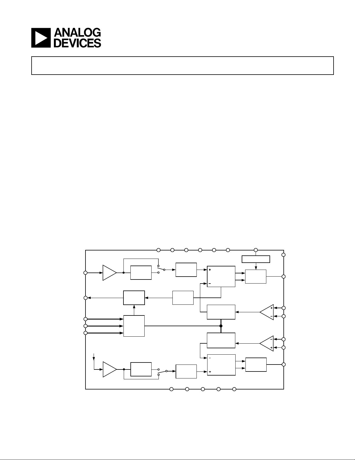
FUNCTIONAL BLOCK DIAGRAM
VDD1 VDD2 VDD3 DVDDVP1 VP2R
ADF4251
REF
IN
2
DOUBLER
GENERAL DESCRIPTION
The ADF4251 is a dual fractional-N/integer-N frequency
synthesizer that can be used to implement local oscillators
(LO) in the upconversion and downconversion sections of
wireless receivers and transmitters. Both the RF and IF synthesizers consist of a low noise digital PFD (phase frequency
detector), a precision charge pump, and a programmable reference divider. The RF synthesizer has a ⌺-⌬ based fractional
interpolator that allows programmable fractional-N division.
The IF synthesizer has programmable integer-N counters. A
complete PLL (phase-locked loop) can be implemented if the
synthesizer is used with an external loop filter and VCO (voltage controlled oscillator).
Control of all the on-chip registers is via a simple 3-wire interface. The devices operate with a power supply ranging from
2.7 V to 3.3 V and can be powered down when not in use.
SET
CE
CP
RF
4-BIT R
COUNTER
PHASE
FREQUENCY
DETECTOR
REFERENCE
CHARGE
PUMP
MUXOUT
CLK
DATA
LE
FROM
REFIN
OUTPUT
MUX
24-BIT
DATA
REGISTER
DOUBLER
2
A
GND
REV. 0
Information furnished by Analog Devices is believed to be accurate and
reliable. However, no responsibility is assumed by Analog Devices for its
use, nor for any infringements of patents or other rights of third parties that
may result from its use. No license is granted by implication or otherwise
under any patent or patent rights of Analog Devices. Trademarks and
registered trademarks are the property of their respective owners.
LOCK
DETECT
FRACTIONAL N
RF DIVIDER
INTEGER N
IF DIVIDER
PHASE
FREQUENCY
15-BIT R
COUNTER
1 A
2 D
GND
One Technology Way, P.O. Box 9106, Norwood, MA 02062-9106, U.S.A.
Tel: 781/329-4700 www.analog.com
Fax: 781/326-8703 © 2003 Analog Devices, Inc. All rights reserved.
DETECTOR
GNDCPGND
1 CP
GND
2
CHARGE
PUMP
RFINA
RF
IN
IFINB
IF
IN
CP
IF
B
A
Page 2

(VDD1 = VDD2 = VDD3 = DVDD = 3 V 10%, VP1 = VP2 = 5 V 10%, GND = 0 V,
1
R
ADF4251–SPECIFICATIONS
= 2.7 k, dBm referred to 50 , TA = T
SET
MIN
to T
, unless otherwise noted.)
MAX
Parameter B Version Unit Test Conditions/Comments
RF CHARACTERISTICS
RF Input Frequency (RF
A, RFINB)
IN
RF Input Sensitivity –10/0 dBm min/max
RF Input Frequency (RF
A, RFINB)
IN
2
2
0.25/3.0 GHz min/max
0.1/3.0 GHz min/max Input Level = –8/0 dBm min/max
RF Phase Detector Frequency 30 MHz max Guaranteed by Design
Allowable Prescaler Output Frequency 375 MHz max
IF CHARACTERISTICS
IF Input Frequency (IF
IN
A, IFINB)
2
50/1200 MHz min/max
IF Input Sensitivity –10/0 dBm min/max
IF Phase Detector Frequency 55 MHz max Guaranteed by Design
Allowable Prescaler Output Frequency 150 MHz max
REFERENCE CHARACTERISTICS
Input Frequency 250 MHz max For f < 10 MHz, use dc-coupled square
REF
IN
wave (0 to V
Input Sensitivity 0.5/VDD1V p-p min/max AC-coupled. When dc-coupled, use
REF
IN
Input Current ±100 µA max
REF
IN
0 to V
DD
).
DD
max (CMOS compatible).
REFIN Input Capacitance 10 pF max
CHARGE PUMP
Sink/Source High Value 4.375 mA typ See Table V
RF I
CP
Low Value 625 µA typ
IF I
Sink/Source High Value 5 mA typ See Table IX
CP
Low Value 625 µA typ
Three-State Leakage Current 1 nA typ
I
CP
RF Sink and Source Current Matching 2 % typ 0.5 V < V
< VP – 0.5
CP
IF Sink and Source Current Matching 2 % typ
I
CP
vs. V
CP
2% typ 0.5 V < VCP < VP – 0.5
ICP vs. Temperature 2 % typ VCP = VP/2
LOGIC INPUTS
, Input High Voltage 1.35 V min
V
INH
V
, Input Low Voltage 0.6 V max
INL
I
, Input Current ±1 µA max
INH/IINL
CIN Input Capacitance 10 pF max
LOGIC OUTPUTS
, Output High Voltage VDD – 0.4 V min IOH = 0.2 mA
V
OH
VOL, Output Low Voltage 0.4 V max IOL = 0.2 mA
POWER SUPPLIES
V
DD1, VDD
DV
1, VP2V
V
P
I
DD
2, VDD3 2.7/3.3 V min/V max
DD
3
RF + IF 13 mA typ 16 mA max
VDD1
1/5.5 V min/V max
DD
RF Only 10 mA typ 13 mA max
IF Only 4 mA typ 5.5 mA max
Low Power Sleep Mode/Power-Down 10 pA typ
RF NOISE AND SPURIOUS CHARACTERISTICS
Noise Floor –141 dBc/Hz typ @ 20 MHz PFD Frequency
In-Band Phase Noise Performance
Lowest Spur Mode –90 dBc/Hz typ RF
Low Noise and Spur Mode –95 dBc/Hz typ RF
Lowest Noise Mode –103 dBc/Hz typ RF
4
@ VCO Output
= 1.8 GHz, PFD = 20 MHz
OUT
= 1.8 GHz, PFD = 20 MHz
OUT
= 1.8 GHz, PFD = 20 MHz
OUT
Spurious Signals See Typical Performance Characteristics
NOTES
1
Operating Temperature Range (B Version): –40°C to +85°C.
2
Use a square wave for frequencies less than F
3
RF = 1 GHz, RF PFD = 10 MHz, MOD = 4095, IF = 500 MHz, IF PFD = 200 kHz, REF = 10 MHz, VDD = 3 V, VP1 = 5 V, and VP2 = 3 V.
4
The in-band phase noise is measured with the EVAL-ADF4251EB2 Evaluation Board and the HP5500E Phase Noise Test System. The spectrum analyzer provides the
REFIN for the synthesizer (f
Specifications subject to change without notice.
= 10 MHz @ 0 dBm). F
REFOUT
MIN
.
= 1.74 GHz, F
OUT
= 20 MHz, N = 87, MOD = 100, Channel Spacing = 200 kHz, VDD = 3.3 V, and VP= 5 V.
REF
REV. 0–2–
Page 3
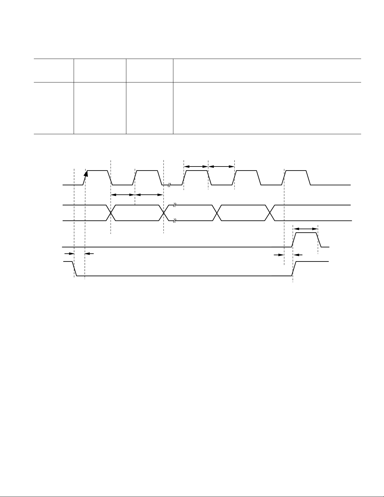
ADF4251
TIMING CHARACTERISTICS
*
(VDD1 = VDD2 = VDD3 = DVDD = 3 V 10%, VP1 = VP2 = 5 V 10%, GND = 0 V, unless otherwise noted.)
Limit at
to T
T
MIN
MAX
Parameter (B Version) Unit Test Conditions/Comments
t
1
t
2
t
3
t
4
t
5
t
6
t
7
*Guaranteed by design but not production tested.
CLOCK
DATA
10 ns min LE Setup Time
10 ns min DATA to CLOCK Setup Time
10 ns min DATA to CLOCK Hold Time
25 ns min CLOCK High Duration
25 ns min CLOCK Low Duration
10 ns min CLOCK to LE Setup Time
20 ns min LE Pulsewidth
DB23
(MSB)
t
4
DB22
t
3
DB2
t
2
t
5
DB1
(CONTROL BIT C2)
DB0 (LSB)
(CONTROL BIT C1)
t
7
LE
t
1
LE
t
6
Figure 1. Timing Diagram
REV. 0
–3–
Page 4

ADF4251
ABSOLUTE MAXIMUM RATINGS
1, 2
(TA = 25°C, unless otherwise noted.)
VDD1, VDD2, VDD3, DVDD to GND3 . . . . . . . . –0.3 V to +4 V
REF
, RFINA, RFINB to GND . . . . . . –0.3 V to VDD + 0.3 V
IN
1, VP2 to GND . . . . . . . . . . . . . . . . . . . . . –0.3 V to +5.8 V
V
P
V
1, VP2 to VDD1 . . . . . . . . . . . . . . . . . . . . . –3.3 V to +3.5 V
P
Digital I/O Voltage to GND . . . . . . . . –0.3 V to V
Analog I/O Voltage to GND . . . . . . . . –0.3 V to V
+ 0.3 V
DD
+ 0.3 V
DD
Operating Temperature Range
Industrial (B Version) . . . . . . . . . . . . . . . . –40°C to +85°C
Storage Temperature Range . . . . . . . . . . . . –65°C to +150°C
Maximum Junction Temperature . . . . . . . . . . . . . . . . . 150°C
LFCSP
Thermal Impedance . . . . . . . . . . . . . . . . 122°C/W
JA
Soldering Reflow Temperature
Vapor Phase (60 sec max) . . . . . . . . . . . . . . . . . . . . . 240°C
IR Reflow (20 sec max) . . . . . . . . . . . . . . . . . . . . . . . 240°C
ORDERING GUIDE
Model Temperature Range Package Option*
ADF4251BCP –40ºC to +85ºC CP-24
ADF4251BCP-REEL –40ºC to +85ºC CP-24
ADF4251BCP-REEL7 –40ºC to +85ºC CP-24
*CP = Lead Frame Chip Scale Package
NOTES
1
Stresses above those listed under Absolute Maximum Ratings may cause permanent damage to the device. This is a stress rating only and functional operation of
the device at these or any other conditions above those listed in the operational
sections of this specification is not implied. Exposure to absolute maximum rating
conditions for extended periods may affect device reliability.
2
This device is a high performance RF integrated circuit with an ESD rating
of <2 kW, and it is ESD sensitive. Proper precautions should be taken for handling
and assembly.
3
GND = CP
GND
1, A
GND
1, D
GND
, A
2, and CP
GND
GND
2.
PIN CONFIGURATION
1
3
2
DD
DD
22 V
9
GND
D
2
P
DD
21 V
20 V
CLK 10
DATA 11
IF
19 CP
LE 12
18 CP
17 DV
16 IFINA
15 IF
IN
14 A
GND
13 R
SET
GND
DD
B
2
2
CP
RF
CP
1 2
GND
RF
A 3
IN
RFINB 4
A
1 5
GND
MUXOUT 6
1
1
P
24 V
23 V
PIN 1
INDICATOR
ADF4251
TOP VIEW
(Not to Scale)
7
IN
CE 8
REF
CAUTION
ESD (electrostatic discharge) sensitive device. Electrostatic charges as high as 4000 V readily
accumulate on the human body and test equipment and can discharge without detection. Although the
ADF4251 features proprietary ESD protection circuitry, permanent damage may occur on devices
subjected to high energy electrostatic discharges. Therefore, proper ESD precautions are recommended
to avoid performance degradation or loss of functionality.
REV. 0–4–
Page 5

ADF4251
PIN FUNCTION DESCRIPTIONS
Mnemonic Function
CP
RF
CP
1 RF Charge Pump Ground
GND
RF
A Input to the RF Prescaler. This small signal input is normally taken from the VCO.
IN
RF
BComplementary Input to the RF Prescaler
IN
A
1Analog Ground for the RF Synthesizer
GND
MUXOUT This multiplexer output allows either the RF or IF lock detect, the scaled RF or IF, or the scaled reference fre-
REF
IN
CE Chip Enable. A Logic Low on this bit powers down the device and puts the charge pump outputs into three-state.
D
GND
CLK Serial Clock Input. This serial clock is used to clock in the serial data to the registers. The data is latched into the
DATA Serial Data Input. The serial data is loaded MSB first with the three LSBs being the control bits. This input is a
LE Load Enable, CMOS Input. When LE goes high, the data stored in the shift registers is loaded into one of the
R
SET
A
2Ground for the IF Synthesizer
GND
IF
BComplementary Input to the IF Prescaler
IN
IF
A Input to the IF Prescaler. This small signal input is normally taken from the IF VCO.
IN
DV
DD
CP
2IF Charge Pump Ground
GND
CP
IF
V
2IF Charge Pump Power Supply. Decoupling capacitors to the ground plane should be placed as close as possible
P
V
2Positive Power Supply for the IF Section. Decoupling capacitors to the ground plane should be placed as close as
DD
V
3 Positive Power Supply for the RF Digital Section. Decoupling capacitors to the ground plane should be placed as close
DD
V
1 Positive Power Supply for the RF Analog Section. Decoupling capacitors to the ground plane should be placed as close
DD
V
1 RF Charge Pump Power Supply. Decoupling capacitors to the ground plane should be placed as close as possible
P
RF Charge Pump Output. This is normally connected to a loop filter that drives the input to an external VCO.
quency to be accessed externally.
Reference Input. This is a CMOS input with a nominal threshold of VDD/2 and an equivalent input resistance of
100 kW. This input can be driven from a TTL or CMOS crystal oscillator.
A Logic High on this pin powers up the device, depending on the status of the software power-down bits.
Digital Ground for the Fractional Interpolator
shift register on the CLK rising edge. This input is a high impedance CMOS input.
high impedance CMOS input.
seven latches, the latch being selected using the control bits.
Connecting a resistor between this pin and ground sets the minimum charge pump output current. The relationship
between I
I
CP MIN
Therefore, with R
=
and R
CP
1 6875.
R
SET
is:
SET
= 2.7 kW, I
SET
= 0.625 mA.
CP MIN
Positive Power Supply for the Fractional Interpolator Section. Decoupling capacitors to the ground plane should
be placed as close as possible to this pin. DV
must have the same voltage as VDD1, VDD2, and VDD3.
DD
IF Charge Pump Output. This is normally connected to a loop filter that drives the input to an external VCO.
to this pin. This voltage should be greater than or equal to V
possible to this pin. V
as possible to this pin. V
as possible to this pin. V
2 has a value 3 V ± 10%. VDD2 must have the same voltage as VDD1, VDD3, and DVDD.
DD
3 has a value 3 V ± 10%. VDD3 must have the same voltage as VDD1, VDD2, and DVDD.
DD
1 has a value 3 V ± 10%. VDD1 must have the same voltage as VDD2, VDD3, and DVDD.
DD
DD
2.
to this pin. This voltage should be greater than or equal to VDD1.
REV. 0
–5–
Page 6
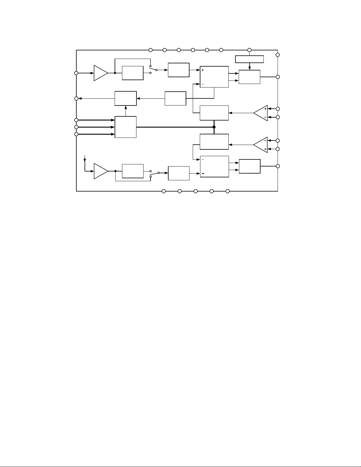
ADF4251
REF
MUXOUT
CLK
DATA
IN
LE
ADF4251
FROM
REFIN
VDD1 VDD2 VDD3 DVDDVP1 VP2R
A
GND
4-BIT R
COUNTER
LOCK
DETECT
15-BIT R
COUNTER
1 A
GND
2 D
PHASE
FREQUENCY
DETECTOR
FRACTIONAL N
RF DIVIDER
INTEGER N
IF DIVIDER
PHASE
FREQUENCY
DETECTOR
GNDCPGND
1 CP
DOUBLER
OUTPUT
MUX
24-BIT
DATA
REGISTER
DOUBLER
2
2
Figure 2. Detailed Functional Block Diagram
GND
REFERENCE
CHARGE
CHARGE
2
SET
PUMP
PUMP
CE
CP
RF
RFINA
RF
IN
IFINB
IF
IN
CP
IF
B
A
REV. 0–6–
Page 7
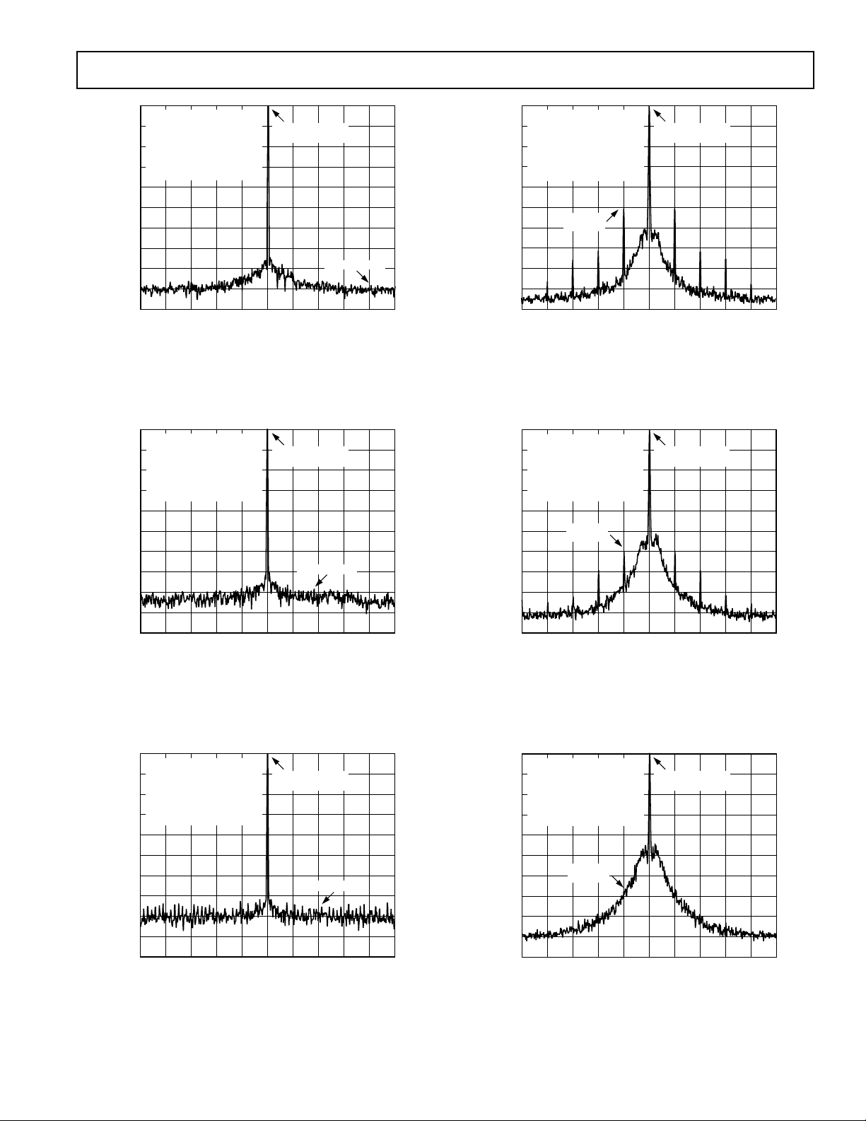
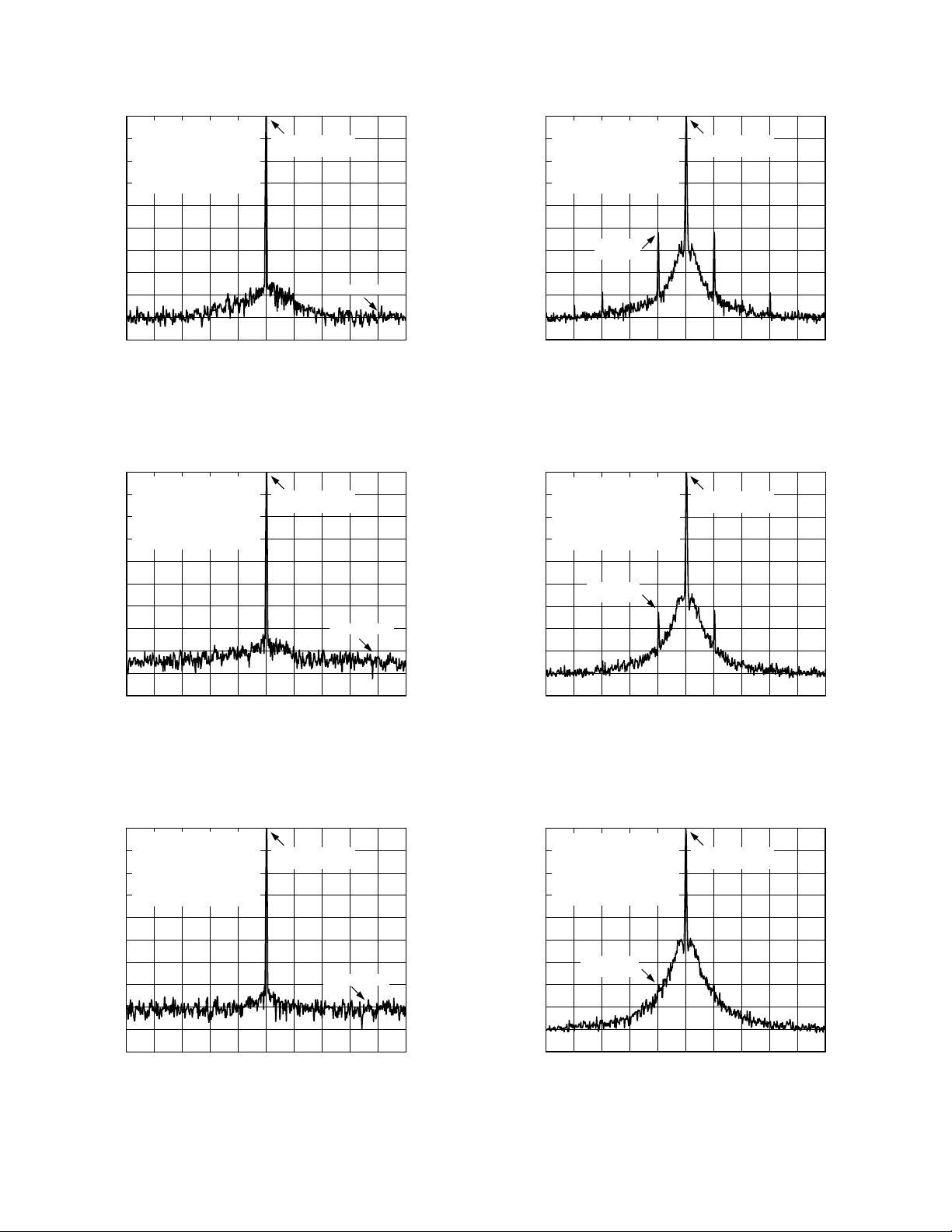
Typical Performance Characteristics–ADF4251
0
VDD = 3V, VP = 5V
= 1.875mA
I
–10
CP
PFD FREQUENCY = 10MHz
–20
CHANNEL STEP = 200kHz
LOOP BANDWIDTH = 20kHz
FRACTION = 59/100
–30
RBW = 10Hz
–40
–50
–60
OUTPUT POWER – dB
–70
–80
–90
–100
–2kHz
–1kHz 1.7518GHz 1kHz 2kHz
REFERENCE
LEVEL = – 4.2dBm
FREQUENCY
–99.19dBc/Hz
TPC 1. Phase Noise Plot, Lowest Noise Mode,
1.7518 GHz RF
, 10 MHz PFD Frequency,
OUT
200 kHz Channel Step Resolution
0
VDD = 3V, VP = 5V
–10
= 1.875mA
I
CP
PFD FREQUENCY = 10MHz
CHANNEL STEP = 200kHz
–20
LOOP BANDWIDTH = 20kHz
FRACTION = 59/100
–30
RBW = 10Hz
–40
–50
–60
OUTPUT POWER – dB
–70
–80
–90
–100
–2kHz
–1kHz 1.7518GHz 1kHz 2kHz
REFERENCE
LEVEL = – 4.2dBm
FREQUENCY
–90.36dBc/Hz
TPC 2. Phase Noise Plot, Low Noise and Spur
Mode, 1.7518 GHz RF
, 10 MHz PFD Frequency,
OUT
200 kHz Channel Step Resolution
0
VDD = 3V, VP = 5V
= 1.875mA
I
–10
CP
PFD FREQUENCY = 10MHz
–20
CHANNEL STEP = 200kHz
LOOP BANDWIDTH = 20kHz
FRACTION = 59/100
–30
RBW = 1kHz
–40
–50
–60
OUTPUT POWER – dB
–70
–80
–90
–100
–50dBc@
100kHz
–400kHz –200kHz 1.7518GHz 200kHz 400kHz
REFERENCE
LEVEL = – 4.2dBm
FREQUENCY
TPC 4. Spurious Plot, Lowest Noise Mode,
1.7518 GHz RF
, 10 MHz PFD Frequency,
OUT
200 kHz Channel Step Resolution
0
VDD = 3V, VP = 5V
–10
= 1.875mA
I
CP
PFD FREQUENCY = 10MHz
CHANNEL STEP = 200kHz
–20
LOOP BANDWIDTH = 20kHz
FRACTION = 59/100
–30
RBW = 1kHz
–40
–50
–60
OUTPUT POWER – dB
–70
–80
–90
–100
–51dBc@
–400kHz
100kHz
–200kHz 1.7518GHz 200kHz 400kHz
REFERENCE
LEVEL = – 4.2dBm
FREQUENCY
TPC 5. Spurious Plot, Low Noise and Spur Mode,
1.7518 GHz RF
, 10 MHz PFD Frequency,
OUT
200 kHz Channel Step Resolution
0
VDD = 3V, VP = 5V
–10
= 1.875mA
I
CP
PFD FREQUENCY = 10MHz
CHANNEL STEP = 200kHz
–20
LOOP BANDWIDTH = 20kHz
FRACTION = 59/100
–30
RBW = 10Hz
–40
–50
–60
OUTPUT POWER – dB
–70
–80
–90
–100
–2kHz
–1kHz 1.7518GHz 1kHz 2kHz
REFERENCE
LEVEL = – 4.2dBm
FREQUENCY
–85.86dBc/Hz
TPC 3. Phase Noise Plot, Lowest Spur Mode,
1.7518 GHz RF
, 10 MHz PFD Frequency,
OUT
200 kHz Channel Step Resolution
0
VDD = 3V, VP = 5V
–10
= 1.875mA
I
CP
PFD FREQUENCY = 10MHz
CHANNEL STEP = 200kHz
–20
LOOP BANDWIDTH = 20kHz
FRACTION = 59/100
–30
RBW = 1kHz
–40
–50
–60
OUTPUT POWER – dB
–70
–80
–90
–100
–400kHz
–72dBc@
100kHz
–200kHz 1.7518GHz 200kHz 400kHz
TPC 6. Spurious Plot, Lowest Spur Mode,
1.7518 GHz RF
, 10 MHz PFD Frequency,
OUT
200 kHz Channel Step Resolution
TPCs 1–12 attained using EVAL-ADF4252EB1 Evaluation Board; measurements from HP8562E spectrum analyzer.
REV. 0
–7–
REFERENCE
LEVEL = – 4.2dBm
FREQUENCY
Page 8
ADF4251
0
VDD = 3V, VP = 5V
= 1.875mA
I
–10
CP
PFD FREQUENCY = 20MHz
CHANNEL STEP = 200kHz
–20
LOOP BANDWIDTH = 20kHz
FRACTION = 59/100
–30
RBW = 10Hz
–40
–50
–60
OUTPUT POWER – dB
–70
–80
–90
–100
–2kHz
–1kHz 1.7518GHz 1kHz 2kHz
REFERENCE
LEVEL = – 4.2dBm
FREQUENCY
–102dBc/Hz
TPC 7. Phase Noise Plot, Lowest Noise Mode,
1.7518 GHz RF
, 20 MHz PFD Frequency,
OUT
200 kHz Channel Step Resolution
0
VDD = 3V, VP = 5V
= 1.875mA
I
–10
CP
PFD FREQUENCY = 20MHz
CHANNEL STEP = 200kHz
–20
LOOP BANDWIDTH = 20kHz
FRACTION = 59/100
–30
RBW = 10Hz
–40
–50
–60
OUTPUT POWER – dB
–70
–80
–90
–100
–2kHz
–1kHz 1.7518GHz 1kHz 2kHz
REFERENCE
LEVEL = – 4.2dBm
FREQUENCY
–93.86dBc/Hz
TPC 8. Phase Noise Plot, Low Noise and Spur
Mode, 1.7518 GHz RF
, 20 MHz PFD Frequency,
OUT
200 kHz Channel Step Resolution
0
VDD = 3V, VP = 5V
= 1.875mA
I
–10
CP
PFD FREQUENCY = 20MHz
CHANNEL STEP = 200kHz
–20
LOOP BANDWIDTH = 20kHz
FRACTION = 59/100
–30
RBW = 1kHz
–40
–50
–60
OUTPUT POWER – dB
–70
–80
–90
–100
–53dBc@
100kHz
–400kHz –200kHz 1.7518GHz 200kHz 400kHz
REFERENCE
LEVEL = – 4.2dBm
FREQUENCY
TPC 10. Spurious Plot, Lowest Noise Mode,
1.7518 GHz RF
, 20 MHz PFD Frequency,
OUT
200 kHz Channel Step Resolution
0
VDD = 3V, VP = 5V
= 1.875mA
I
–10
CP
PFD FREQUENCY = 20MHz
CHANNEL STEP = 200kHz
–20
LOOP BANDWIDTH = 20kHz
FRACTION = 59/100
–30
RBW = 1kHz
–40
–50
–60
OUTPUT POWER – dB
–70
–80
–90
–100
–63.2dBc@
–400kHz
100kHz
–200kHz 1.7518GHz 200kHz 400kHz
REFERENCE
LEVEL = – 4.2dBm
FREQUENCY
TPC 11. Spurious Plot, Low Noise and Spur Mode,
1.7518 GHz RF
, 20 MHz PFD Frequency, 200 kHz
OUT
Channel Step Resolution
0
VDD = 3V, VP = 5V
= 1.875mA
I
–10
CP
PFD FREQUENCY = 20MHz
CHANNEL STEP = 200kHz
–20
LOOP BANDWIDTH = 20kHz
FRACTION = 59/100
–30
RBW = 10Hz
–40
–50
–60
OUTPUT POWER – dB
–70
–80
–90
–100
–2kHz
–1kHz 1.7518GHz 1kHz 2kHz
REFERENCE
LEVEL = – 4.2dBm
FREQUENCY
–89.52dBc/Hz
TPC 9. Phase Noise Plot, Lowest Spur Mode,
1.7518 GHz RF
, 20 MHz PFD Frequency,
OUT
200 kHz Channel Step Resolution
0
VDD = 3V, VP = 5V
= 1.875mA
I
–10
CP
PFD FREQUENCY = 20MHz
CHANNEL STEP = 200kHz
–20
LOOP BANDWIDTH = 20kHz
FRACTION = 59/100
–30
RBW = 1kHz
–40
–50
–60
OUTPUT POWER – dB
–70
–80
–90
–100
–72.33dBc@
–400kHz
100kHz
–200kHz 1.7518GHz 200kHz 400kHz
REFERENCE
LEVEL = – 4.2dBm
FREQUENCY
TPC 12. Spurious Plot, Lowest Spur Mode,
1.7518 GHz RF
, 20 MHz PFD Frequency,
OUT
200 kHz Channel Step Resolution
REV. 0–8–
Page 9
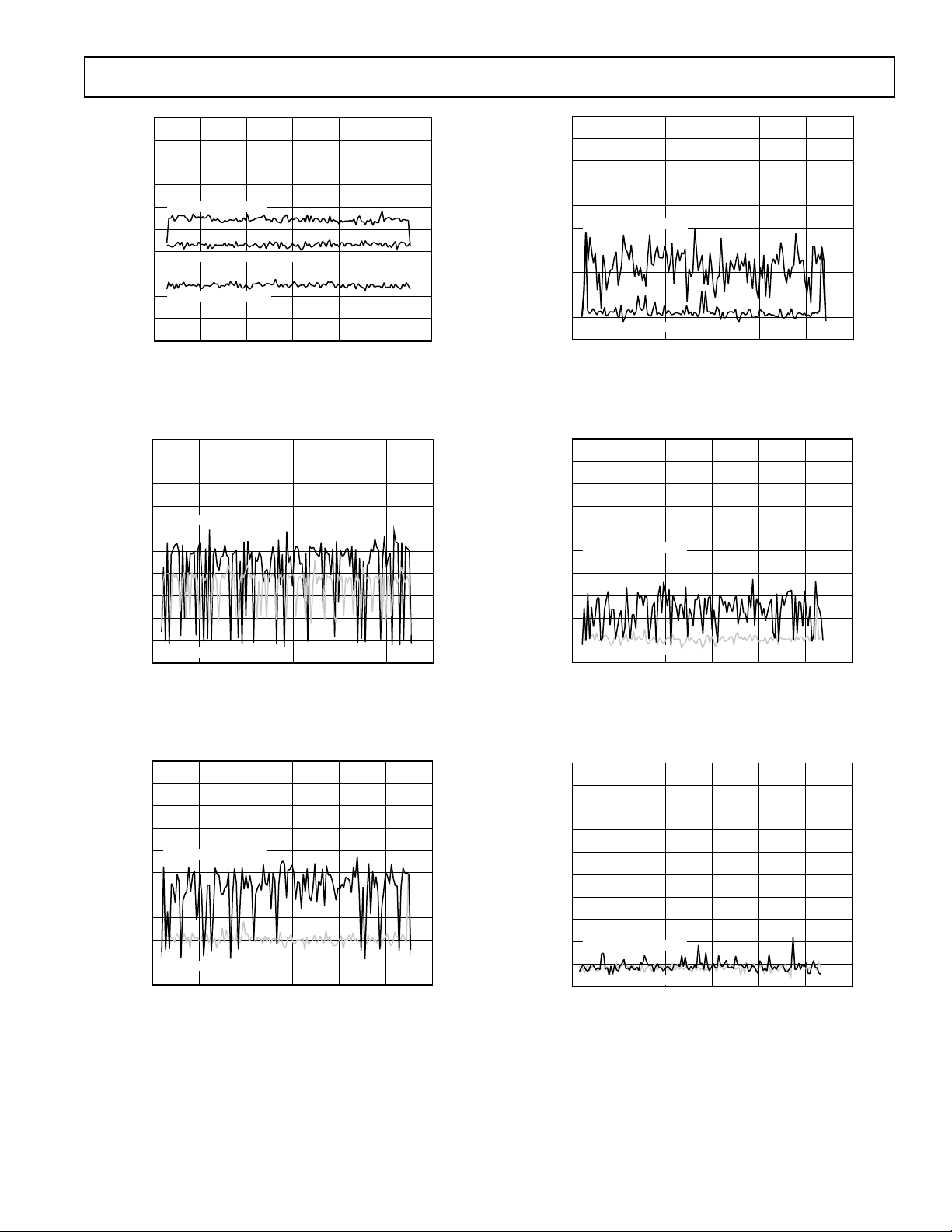
ADF4251
–70
–75
–80
–85
LOWEST SPUR MODE
–90
–95
–100
LOW NOISE AND SPUR MODE
–105
PHASE NOISE – dBc/Hz
LOWEST NOISE MODE
–110
–115
–120
1.430 1.4601.435
1.440 1.445 1.450 1.455
FREQUENCY – GHz
TPC 13. In-Band Phase Noise vs. Frequency
–10
–20
–30
–40
LOWEST NOISE MODE
–50
–60
–70
–80
SPURIOUS LEVEL – dBc
–90
–100
LOWEST SPUR MODE
–110
1.430 1.4601.435
TPC 14. 100 kHz Spur vs. Frequency
1.440 1.445 1.450 1.455
FREQUENCY – GHz
*
–20
–30
–40
–50
–60
LOWEST NOISE MODE
–70
–80
–90
SPURIOUS LEVEL – dBc
–100
–110
LOWEST SPUR MODE
–120
1.430 1.4601.435
*
TPC 16. 400 kHz Spur vs. Frequency
–20
–30
–40
–50
–60
LOWEST NOISE MODE
–70
–80
–90
SPURIOUS LEVEL – dBc
–100
–110
LOWEST SPUR MODE
–120
1.430 1.4601.435
TPC 17. 600 kHz Spur vs. Frequency
1.440 1.445 1.450 1.455
FREQUENCY – GHz
*
1.440 1.445 1.450 1.455
FREQUENCY – GHz
*
–20
–30
–40
–50
–60
LOWEST NOISE MODE
–70
–80
–90
SPURIOUS LEVEL – dBc
–100
–110
LOWEST SPUR MODE
–120
1.430 1.4601.435
1.440 1.445 1.450 1.455
FREQUENCY – GHz
TPC 15. 200 kHz Spur vs. Frequency
*
–20
–30
–40
–50
–60
–70
–80
–90
SPURIOUS LEVEL – dBc
–100
LOWEST NOISE MODE
–110
LOWEST SPUR MODE
–120
1.430 1.4601.435
1.440 1.445 1.450 1.455
FREQUENCY – GHz
TPC 18. 3 MHz Spur vs. Frequency
*TPCs 13–18: Across all fractional channel steps from f = 0/130 to f = 129/130.
RF
= 1.45 GHz, Int Reg = 55, Ref = 26 MHz, and LBW = 40 kHz. TPCs 13–24 attained using EVAL-ADF4252EB2 Evaluation Board.
OUT
REV. 0
–9–
*
Page 10

ADF4251
0
–5
–10
–15
–20
AMPLITUDE – dBm
–25
–30
–35
PRESCALER = 4/5
061
TPC 19. RF Input Sensitivity
0
VDD = 3V
VP2 = 3V
5
10
15
20
25
IF INPUT POWER – dBm
30
35
40
–0.4 1.60.1
TPC 20. IF Input Sensitivity
PRESCALER = 8/9
2345
FREQUENCY –GHz
0.6 1.1
IF INPUT FREQUENCY – GHz
–120
VDD = 3V
= 3V
V
P
–130
–140
–150
–160
PHASE NOISE – dB/Hz
–170
–180
10k 10M100k
PHASE DETECTOR FREQUENCY – Hz
1M
TPC 22. Phase Noise (Referred to CP Output) vs.
PFD Frequency, IF Side
6
4
2
VDD = 3V
VP1 = 5.5V
0
– mA
CP
I
–2
–4
–6
00.5
1.5
1.0 2.0 3.0
2.5
VCP – V
4.03.5 4.5 5.5
5.0
TPC 23. RF Charge Pump Output Characteristics
–120
VDD = 3V
= 5V
V
P
–130
–140
–150
–160
PHASE NOISE – dB/Hz
–170
–180
10k
100k
PHASE DETECTOR FREQUENCY – Hz
1M
10M
TPC 21. Phase Noise (Referred to CP Output) vs.
PFD Frequency, RF Side
6
4
2
V
= 3V
DD
VP2 = 3V
0
– mA
CP
I
–2
–4
–6
0
0.5
1.0 2.0 3.0
1.5
VCP – V
2.5
TPC 24. IF Charge Pump Output Characteristics
REV. 0–10–
Page 11

ADF4251
CIRCUIT DESCRIPTION
Reference Input Section
The reference input stage is shown in Figure 3. SW1 and SW2
are normally closed switches. SW3 is normally open. When
power-down is initiated, SW3 is closed and SW1 and SW2 are
opened. This ensures that there is no loading of the REF
pin
IN
on power-down.
POWER-DOWN
CONTROL
100k
NC
NO
SW2
SW3
BUFFER
XOEB
TO R
COUNTER
REF
OUT
REF
IN
NC
SW1
NC = NORMALLY CLOSED
NO = NORMALLY OPEN
Figure 3. Reference Input Stage
RF and IF Input Stage
The RF input stage is shown in Figure 4. The IF input stage is
the same. It is followed by a two-stage limiting amplifier to
generate the CML clock levels needed for the N counter.
BIAS
GENERATOR
A
RF
IN
B
RF
IN
1.6V
V
1
DD
2k2k
A
GND
Figure 4. RF Input Stage
RF INT Divider
The RF INT CMOS counter allows a division ratio in the PLL
feedback counter. Division ratios from 31 to 255 are allowed.
INT, FRAC, MOD, and R Relationship
The INT, FRAC, and MOD values, in conjunction with the
RF R counter, make it possible to generate output frequencies
that are spaced by fractions of the RF phase frequency detector
(PFD). The equation for the RF VCO frequency (RF
RF F INT
=¥ +
OUT PFD
where RF
is the output frequency of external voltage controlled
OUT
Ê
Á
Ë
FRAC
MOD
ˆ
˜
¯
OUT
) is
(1)
oscillator (VCO).
1
D
+
FREF
=¥
PFD IN
()
R
(2)
REFIN = the reference input frequency, D = RF REFIN Doubler
Bit, R = the preset divide ratio of the binary 4-bit programmable reference counter (1 to 15), INT = the preset divide ratio of
the binary 8-bit counter (31 to 255), MOD = the preset modulus
ratio of binary 12-bit programmable FRAC counter (2 to 4095),
and FRAC = the preset fractional ratio of the binary 12-bit
programmable FRAC counter (0 to MOD).
FROM RF
INPUT STAGE
RF N DIVIDER
N-COUNTER
INT
REG
N = INT + FRAC/MOD
THIRD-ORDER
FRACTIONAL
INTERPOLATOR
MOD
REG
FRAC
VALUE
TO PFD
Figure 5. N Counter
RF R Counter
The 4-bit RF R counter allows the input reference frequency
(REF
) to be divided down to produce the reference clock to
IN
the RF PFD. Division ratios from 1 to 15 are allowed.
IF R Counter
The 15-bit IF R counter allows the input reference frequency
(REF
) to be divided down to produce the reference clock to
IN
the IF PFD. Division ratios from 1 to 32767 are allowed.
IF Prescaler (P/P + 1)
The dual modulus IF prescaler (P/P + 1), along with the IF A
and B counters, enables the large division ratio, N, to be realized
(N = PB + A). Operating at CML levels, it takes the clock from
the IF input stage and divides it down to a manageable frequency
for the CMOS IF A and CMOS IF B counters.
IF A and B Counters
The IF A CMOS and IF B CMOS counters combine with the
dual modulus IF prescaler to allow a wide ranging division ratio
in the PLL feedback counter. The counters are guaranteed to
work when the prescaler output is 150 MHz or less.
Pulse Swallow Function
The IF A and IF B counters, in conjunction with the dual modulus
IF prescaler, make it possible to generate output frequencies
that are spaced only by the reference frequency divided by R.
See the Device Programming after Initial Power-Up section for
examples. The equation for the IF VCO (IF
IF P B A F
=¥
()
[]
OUT PFD
where IF
= the output frequency of the external voltage controlled
OUT
+
¥
) frequency is
OUT
(3)
oscillator (VCO), P = the preset modulus of the IF dual modulus
prescaler, B = the preset divide ratio of the binary 12-bit counter
(3 to 4095), and A = the preset divide ratio of the binary 6-bit
swallow counter (0 to 63). F
is obtained using Equation 2.
PFD
REV. 0
–11–
Page 12

ADF4251
Phase Frequency Detector (PFD) and Charge Pump
The PFD takes inputs from the R counter and N counter and
produces an output proportional to the phase and frequency
difference between them. Figure 6 is a simplified schematic. The
PFD includes a delay element that controls the width of the
antibacklash pulse. This pulse ensures that there is no dead zone
in the PFD transfer function and minimizes phase noise and
reference spurs.
U1
HI
D1
UP
Q1
+IN
–IN
CLR1
CHARGE
PUMP
DELAY
ELEMENT
CLR2
HI
D2
DOWN
Q2
U2
U3
CP
Figure 6. PFD Simplified Schematic
MUXOUT and Lock Detect
The output multiplexer on the ADF4251 allows the user to
access various internal points on the chip. The state of MUXOUT
is controlled by M4, M3, M2, and M1 in the Master Register.
Table VI shows the full truth table. Figure 7 shows the MUXOUT
section in block diagram format.
DV
IF ANALOG LOCK DETECT
LOGIC LOW
IF R DIVIDER OUTPUT
IF N DIVIDER OUTPUT
RF ANALOG LOCK DETECT
IF/RF ANALOG LOCK DETECT
IF DIGITAL LOCK DETECT
LOGIC HIGH
RF R DIVIDER OUTPUT
RF N DIVIDER OUTPUT
THREE STATE OUTPUT
RF DIGITAL LOCK DETECT
RF/IF DIGITAL LOCK DETECT
LOGIC HIGH
LOGIC LOW
MUX CONTROL
DD
MUXOUT
D
GND
Figure 7. MUXOUT Circuit
Lock Detect
MUXOUT can be programmed for two types of lock detect: digital
and analog. Digital is active high. The N-channel open-drain
analog lock detect should be operated with an external pull-up
resistor of 10 kW nominal. When lock has been detected, this
output will be high with narrow low going pulses.
Hardware Power-Down/Chip Enable
In addition to the software power-down methods described on
pages 21 and 22, the ADF4251 also has a hardware powerdown feature. This is accessed via the Chip Enable (CE) pin.
When this pin is Logic High, the device is in normal operation.
Bringing the CE pin Logic Low will power down the device.
When this happens, the following events occur:
1. All active dc current paths are removed.
2. The RF and IF counters are forced to their load
state conditions.
3. The RF and IF charge pumps are forced into three-state mode.
4. The digital lock detect circuitry is reset.
5. The RF
6. The REF
and IFIN inputs are debiased.
IN
input buffer circuitry is disabled.
IN
7. The serial interface input register remains active and capable
of loading and latching data.
Bringing the CE pin back up again to Logic High will reinstate
normal operation, depending on the software power-down settings.
Input Shift Register
Data is clocked in on each rising edge of CLK. The data is
clocked in MSB first. Data is transferred from the input register
to one of seven latches on the rising edge of LE. The destination
latch is determined by the state of the three control bits (C2, C1,
and C0) in the shift register. These are the three LSBs: DB2,
DB1, and DB0, as shown in Figure 1. The truth table for these
bits is shown in Table I. Table II shows a summary of how the
registers are programmed.
Table I. Control Bit Truth Table
C2 C1 C0 Data Latch
000 RF N Divider Reg
001 RF R Divider Reg
010 RF Control Reg
011 Master Reg
100 IF N Divider Reg
101 IF R Divider Reg
110 IF Control Reg
REV. 0–12–
Page 13

RF N DIVIDER REG
ADF4251
Table II. Register Summary
RESERVED
DB23 DB22
N8
P1
8-BIT RF INTEGER VALUE (INT)
DB21
DB20 DB19 DB18 DB17 DB16 DB15 DB14 DB13 DB12 DB11 DB10
N6
N7
N4N5
RF R DIVIDER REG
IN
RF REF
DOUBLER
PRES CALER
DB20 DB19 DB18 DB17 DB16 DB15 DB14 DB13 DB12 DB11 DB10 DB9 DB8 DB7 DB6 DB5 DB4 DB3 DB2 DB1 DB0
P2
P3
N2
4-BIT RF R COUNTER
R4
R2
R1R3
RF CONTROL REG
SPUR
SETTING 3
NOISE AND
DB15 DB14 DB13 DB12 DB11 DB10 DB9 DB8 DB7 DB6 DB5 DB4 DB3 DB2 DB1 DB0
M11M12
RESERVED
12-BIT RF FRACTIONAL VALUE (FRAC)
DB9 DB8 DB7 DB6 DB5 DB4 DB3 DB2 DB1 DB0
F8
F9F10F11F12N1N3
12-BIT INTERPOLATOR MODULUS VALUE (MOD)
M8
M9M10
RF CP
CURRENT
SPUR
SETTING
SETTING 2
NOISE AND
MASTER REG
DB10 DB9 DB8 DB7 DB6 DB5 DB4 DB3 DB2 DB1 DB0
M7
MUXOUT
M6
RF PD
RESERVED
POLARITY
M4M5
SPUR
SETTING 1
NOISE AND
RESERVED
RF
POWER-
DOWN
POWER-
DOWN
M2M3
RF CP
STATE
THREE-
STATE
CP THREE-
F1F2F3F4F5F6F7
M1
RF
COUNTER
RESET
COUNTER
C3 (0)
C3 (0)
RESET
C3 (0)
C3 (0)
CONTROL
BITS
C2 (0)
CONTROL
BITS
C2 (0) C1 (1)
CONTROL
BITS
C2 (1) C1 (0)P4P5P6N1P8 0CP1CP2N2T1T2T3N3
CONTROL
BITS
C2 (1) C1 (1)P9P10P11M1M2M3M4
C1 (0)
IF N DIVIDER REG
IF PD
6-BIT IF A COUNTER12-BIT IF B COUNTER
POLARITY
IF LDP
IF POWER-
IF PRESCALER
IF CP GAIN
DB20 DB19 DB18 DB17 DB16 DB15 DB14 DB13 DB12 DB11 DB10 DB9 DB8 DB7 DB6 DB5 DB4 DB3 DB2 DB1 DB0
DB21
DB22DB23
P14P15 C3 (1)
IF R DIVIDER REG
IN
IF REF
DOUBLER
DB18 DB17 DB16 DB15 DB14 DB13 DB12 DB11 DB10 DB9 DB8 DB7 DB6 DB5 DB4 DB3 DB2 DB1 DB0
IF CONTROL REG
RF PHASE
RESYNC
DB15 DB14 DB13 DB12 DB11 DB10 DB9 DB8 DB7 DB6 DB5 DB4 DB3 DB2 DB1 DB0
RESERVED
15-BIT IF R COUNTER
IF CP CURRENT
SETTING
RESYNC
RF PHASE
CONTROL
BITS
C2 (0) C1 (0)A1A2A3A4A5B1B2B3B4B5B6B7B8B9B10B11B12P13 A6
CONTROL
BITS
C2 (0) C1 (1)R1R2R3R4R5R6R7R8R9R10R11R12R13R15P16
C3 (1)R14
RESET
COUNTER
C3 (1)
CONTROL
BITS
C2 (1) C1 (0)P17P18P19P20P21CP1CP2CP3PR1T7T8PR2PR3
IF
IF CP
DOWN
STATE
THREE-
REV. 0
–13–
Page 14

ADF4251
Table III. RF N Divider Register Map
8-BIT RF INTEGER VALUE (INT)
RESERVED
DB21
DB23 DB22
N8
P1
P1 RESERVED
0RESERVED
N8 N7 N6 N5 N4 N3 N2 N1
00011111 31
00100000 32
00100001 33
00100010 34
........ .
........ .
........ .
11111101 253
11111110 254
11111111 255
DB20 DB19 DB18 DB17 DB16 DB15 DB14 DB13 DB12 DB11 DB10 DB9 DB8 DB7 DB6 DB5 DB4 DB3 DB2 DB1 DB0
N7
N6
N4N5
N2
F12 F11 F10 F3 F2 F1 FRACTIONAL VALUE (FRAC)
000.......... 0 0 0 0
000.......... 0 0 1 1
000.......... 0 1 0 2
000.......... 0 1 1 3
............. . . . .
............. . . . .
............. . . . .
111.......... 1 0 0 4092
111.......... 1 0 1 4093
111.......... 1 1 0 4094
111.......... 1 1 1 4095
12-BIT RF FRACTIONAL VALUE (FRAC)
F8
F9F10F11F12N1N3
RF INTEGER
VALU E (INT)*
C3 (0)
CONT ROL
BITS
C2 (0)
C1 (0)F1F2F3F4F5F6F7
*WHEN P = 8/9, N
MIN
= 91
REV. 0–14–
Page 15

Table IV. RF R Divider Register Map
ADF4251
IN
RF REF
DOUBLER
DOUBLER
4-BIT RF R COUNTER
R2
M12 M11 M10 M3 M2 M1 VALUE (MOD) DIVIDE RATIO
IN
R4 R3 R2 R1 DIVIDE RATIO
00011
00102
00113
.....
.....
.....
110113
111014
111115
000.......... 0102
000.......... 0113
000.......... 1004
............. . . . .
............. . . . .
............. . . . .
111.......... 1004092
111.......... 1014093
111.......... 1104094
111.......... 1114095
PRE-
SCALER
DB20 DB19 DB18 DB17 DB16 DB15 DB14 DB13 DB12 DB11 DB10 DB9 DB8 DB7 DB6 DB5 DB4 DB3 DB2 DB1 DB0
P3
P2 RF REF
0DISABLED
1ENABLED
P3 RF PRESCALER
04/5
18/9
12-BIT INTERPOLATOR MODULUS VALUE (MOD)
M9M10M11M12R1R3R4P2
M8
RF R COUNTER
M1M2M3M4M5M6M7
INTERPOLATOR MODULUS
C3 (0)
CONT ROL
BITS
C2 (0) C1 (1)
REV. 0
–15–
Page 16

ADF4251
Table V. RF Control Register Map
SPUR
NOISE AND
DB15 DB14 DB13 DB12 DB11 DB10 DB9 DB8 DB7 DB6 DB5 DB4 DB3 DB2 DB1 DB0
N3 N2 N1 NOISE AND SPUR
SETTING
000LOWEST SPUR
001LOW NOISE AND SPUR
111LOWEST NOISE
RESERVED
SETTING 3
THESE BITS SHOULD
EACH BE SET TO 0 FOR
NORMAL OPERATION
CP2 CP1 1.5k 2.7k 5.6k
001.125 0.625 0.301
013.375 1.875 0.904
105.625 3.125 1.506
117.7875 4.375 2.109
SPUR
SETTING 2
NOISE AND
N2T1T2T3N3
RF CP
CURRENT
SETTING
CP2
I
(mA)
CP
RF PD
RESERVED
POLARITY
SPUR
SETTING 1
NOISE AND
RF CP
DOWN
RF POWER-
P6 RF POWER-DOWN
0DISABLED
1ENABLED
RESET
C3 (0)
RESET
CONT ROL
BITS
C2 (1) C1 (0)P4P5P6N1P8 0CP1
RF
STAT E
THREE-
COUNTER
P4 RF COUNTER
0DISABLED
1ENABLED
P5 RF CP THREE-STATE
0DISABLED
1THREE-STATE
P8 RF PD POLARITY
0NEGATIVE
1POSITIVE
REV. 0–16–
Page 17

Table VI. Master Register Map
ADF4251
MUXOUT
DB10 DB9 DB8 DB7 DB6 DB5 DB4 DB3 DB2 DB1 DB0
MUXOUT
M4
0 0 0 0 LOGIC LOW
0 0 0 1 IF ANALOG LOCK DETECT
0 0 1 0 IF R DIVIDER OUTPUT
0 0 1 1 IF N DIVIDER OUTPUT
0 1 0 0 RF ANALOG LOCK DETECT
0 1 0 1 RF/IF ANALOG LOCK DETECT
0 1 1 0 IF DIGITAL LOCK DETECT
0 1 1 1 LOGIC HIGH
1 0 0 0 RF R DIVIDER OUTPUT
1 0 0 1 RF N DIVIDER OUTPUT
1 0 1 0 THREE-STATE OUTPUT
1 0 1 1 LOGIC LOW
1 1 0 0 RF DIGITAL LOCK DETECT
1 1 0 1 RF/IF DIGITAL LOCK DETECT
1 1 1 0 LOGIC HIGH
1 1 1 1 LOGIC LOW
M2M3
M1
CONT ROL
STAT E
DOWN
POWE R-
RESERVED
P10
0
1
P11
POWER-DOWN
DISABLED
0
ENABLED
1
RESERVED
P12
0 THIS BIT SHOULD BE SET TO “0” FOR
NORMAL OPERATION.
RESET
COUNTER
CP THREE-
P9
0
1
CP THREE-STATE
DISABLED
THREE-STATE
BITS
C2 (1) C1 (1)P9P10P11M1M2M3M4
C3 (0)
COUNTER RESET
DISABLED
ENABLED
REV. 0
–17–
Page 18

ADF4251
Table VII. IF N Divider Register Map
IF
PRESCALER*
GAIN
IF CP
DB21
DB22DB23
P14
P15
P14 P13 PRESCALER VALUE
00 8/9
01 16/17
10 32/33
11 64/65
P15 IF CP GAIN
0DISABLED
1ENABLED
DB19 DB18 DB17 DB16 DB15 DB14 DB13 DB12 DB11
DB20
B12 B11 B10 B3 B2 B1 B COUNTER DIVIDE RATIO
000.......... 0113
000.......... 1004
............. ....
............. ....
............. ....
111.......... 1004092
111.......... 1014093
111.......... 1104094
111.......... 1114095
DB10 DB9 DB8 DB7 DB6 DB5 DB4 DB3 DB2 DB1 DB0
A6 A5 .......... A2 A1 DIVIDE RATIO
00.......... 0 0 0
00.......... 0 1 1
00.......... 1 0 2
00.......... 1 1 3
............ . . .
............ . . .
............ . . .
11.......... 0 0 60
11.......... 0 1 61
11.......... 1 0 62
11.......... 1 1 63
6-BIT IF A COUNTER*12-BIT IF B COUNTER*
A1A2A3A4A5B1B2B3B4B5B6B7B8B9B10B11B12P13 A6
C3 (1)
CONTROL
BITS
C2 (0) C1 (0)
A COUNTER
*N = BP + A, P IS PRESCALER VALUE. B MUST BE GREATER THAN OR EQUAL TO A FOR CONTIGUOUS VALUES OF N, N
IS (P2 – P) .
MIN
REV. 0–18–
Page 19

Table VIII. IF R Divider Register Map
ADF4251
IN
IF REF
DOUBLER
DB18 DB17 DB16 DB15 DB14 DB13 DB12 DB11 DB10 DB9 DB8 DB7 DB6 DB5 DB4 DB3 DB2 DB1 DB0
R14
R14 R13 R12 .......... R3 R2 R1 DIVIDE RATIO
000.......... 0011
000.......... 0102
000.......... 0113
000.......... 1004
............. ....
............. ....
............. ....
111.......... 10016380
111.......... 10116381
111.......... 11016382
111.......... 11116383
P16 IF REF
0DISABLED
1ENABLED
IN
DOUBLER
R15
0
0
0
0
.
.
.
32764
32765
32766
32767
15-BIT IF R COUNTER
R8
R9R10R11R12R13R15P16
C3 (1)
CONT ROL
BITS
C2 (0) C1 (1)R1R2R3R4R5R6R7
REV. 0
–19–
Page 20

ADF4251
Table IX. IF Control Register Map
RF PHASE
RESYNC
DB15 DB14 DB13 DB12 DB11 DB10 DB9 DB8 DB7 DB6 DB5 DB4 DB3 DB2 DB1 DB0
PR3 PR2 PR1 RF PHASE RESYNC
000DISABLED
111ENABLED
IF CP3 IF CP2 IF CP1 1.5k 2.7k 5.6k
000 1.1250.625 0.301
001 2.251.25 0.602
010 3.3751.875 0.904
011 4.52.51.205
100 5.6253.125 1.506
101 6.753.75 1.808
110 7.78754.375 2.109
111 95.02.411
RESERVED
THESE BITS
SHOULD BE SET
TO 0 FOR NORMAL
OPERATION
RESYNC
RF PHASE
PR1T7T8PR2PR3
IF CP CURRENT
SETTING
CP3
I
(mA)
CP
IF PD
POLARITY
P20 IF LDP
0 3
1 5
P21 IF PD POLARITY
0 NEGATIVE
1 POSITIVE
DOWN
IF LDP
IF POWER-
P19 IF POWER-DOWN
0 DISABLED
1 ENABLED
IF
IF CP
STAT E
RESET
THREE-
COUNTER
P17 IF COUNTER RESET
0 DISABLED
1 ENABLED
P18 IF CP THREE-STATE
0 DISABLED
1 THREE-STATE
C3 (1)
CONT ROL
BITS
C2 (1) C1 (0)P17P18P19P20P21CP1CP2
REV. 0–20–
Page 21

ADF4251
RF N DIVIDER REGISTER
(Address R0)
With R0[2, 1, 0] set to [0, 0, 0], the on-chip RF N Divider register
will be programmed. Table III shows the input data format for
programming this register.
8-Bit RF INT Value
These eight bits control what is loaded as the INT value. This is
used to determine the overall feedback division factor. It is used in
Equation 1.
12-Bit RF FRAC Value
These 12 bits control what is loaded as the FRAC value into the
fractional interpolator. This is part of what determines the overall
feedback division factor. It is used in Equation 1. The FRAC
value must be less than or equal to the value loaded into the
MOD register.
RF R DIVIDER REGISTER
(Address R1)
With R1[2, 1, 0] set to [0, 0, 1], the on-chip RF R Divider register
will be programmed. Table IV shows the input data format for
programming this register.
RF Prescaler (P/P + 1)
The RF dual-modulus prescaler (P/P +1), along with the INT,
FRAC, and MOD counters, determine the overall division ratio
from the RF
to the PFD input. Operating at CML levels, it
IN
takes the clock from the RF input stage and divides it down to
amanageable frequency for the CMOS counters. It is based on
a synchronous 4/5 core (see Table IV).
RF REFIN Doubler
Setting this bit to 0 feeds the REFIN signal directly to the 4-bit
RF R counter, disabling the doubler. Setting this bit to 1 multiplies
the REF
bit RF R counter. When the doubler is disabled, the REF
frequency by a factor of 2 before feeding into the 4-
IN
IN
falling edge is the active edge at the PFD input to the fractional-N
synthesizer. When the doubler is enabled, both the rising and
falling edges of REF
become active edges at the PFD input.
IN
When the doubler is enabled and lowest spur mode is chosen,
the in-band phase noise performance is sensitive to the REF
IN
duty cycle. The phase noise degradation can be as much as 5 dB
for REF
noise is insensitive to REF
duty cycles outside a 45% to 55% range. The phase
IN
duty cycle in the lowest noise mode
IN
and in low noise and spur mode. The phase noise is insensitive
to REF
duty cycle when the doubler is disabled.
IN
4-Bit RF R Counter
The 4-bit RF R counter allows the input reference frequency
) to be divided down to produce the reference clock to
(REF
IN
the phase frequency detector (PFD). Division ratios from 1 to
15 are allowed.
12-Bit Interpolator Modulus
This programmable register sets the fractional modulus. This is
the ratio of the PFD frequency to the channel step resolution on
the RF output.
RF CONTROL REGISTER
(Address R2)
With R2[2, 1, 0] set to [0, 1, 0], the on-chip RF control register
will be programmed. Table V shows the input data format for
programming this register. Upon initialization, DB15–DB11
should all be set to 0.
Noise and Spur Setting
The noise and spur setting (R2[15, 11, 06]) is a feature that
allows the user to optimize his or her design either for improved
spurious performance or for improved phase noise performance.
When set to [0, 0, 0], the lowest spurs setting is chosen. Here,
dither is enabled. This randomizes the fractional quantization
noise so that it looks more like white noise than spurious noise.
This means that the part is optimized for improved spurious
performance. This operation would normally be used when the
PLL closed-loop bandwidth is wide
A wide loop filter does not attenuate the spurs to a level that a
2
narrow
loop bandwidth would. When this bit is set to [0, 0, 1],
1
for fast-locking applications.
the low noise and spur setting is enabled. Here, dither is disabled.
This optimizes the synthesizer to operate with improved noise
performance. However, the spurious performance is degraded in
this mode compared to lowest spurs setting. To improve noise
performance even further, another option is available that reduces
the phase noise. This is the lowest noise setting [1, 1, 1]. As well
as disabling the dither, it also ensures the charge pump is operating in an optimum region for noise performance. This setting is
extremely useful where a narrow loop filter bandwidth is available.
The synthesizer ensures extremely low noise and the filter attenuates the spurs. The Typical Performance Characteristics (TPCs)
give the user an idea of the trade-off in a typical WCDMA setup
for the different noise and spur settings.
RF Counter Reset
DB3 is the RF counter reset bit for the ADF4251. When this is
1, the RF synthesizer counters are held in reset. For normal
operation, this bit should be 0.
RF Charge Pump Three-State
This bit puts the charge pump into three-state mode when programmed to a 1. It should be set to 0 for normal operation.
RF Power-Down
DB5 on the ADF4251 provides the programmable power-down
mode. Setting this bit to a 1 will perform a power-down on both
the RF and IF sections. Setting this bit to 0 will return the RF
and IF sections to normal operation. While in software powerdown, the part will retain all information in its registers. Only
when supplies are removed will the register contents be lost.
When a power-down is activated, the following events occur:
1. All active RF dc current paths are removed.
2. The RF synthesizer counters are forced to their load state
conditions.
3. The RF charge pump is forced into three-state mode.
4. The RF digital lock detect circuitry is reset.
5. The RF
input is debiased.
IN
6. The input register remains active and capable of loading and
latching data.
NOTES
1
Wide loop bandwidth is seen as a loop bandwidth greater than 1/10th of the
RF
channel step resolution (F
OUT
2
Narrow loop bandwidth is seen as a loop bandwidth less than 1/10th of the
RF
channel step resolution (F
OUT
RES
RES
).
).
REV. 0
–21–
Page 22

ADF4251
RF Phase Detector Polarity
DB7 in the ADF4251 sets the RF phase detector polarity.
When the VCO characteristics are positive, this should be set to 1.
When they are negative, it should be set to 0.
RF Charge Pump Current Setting
DB9 and DB10 set the RF charge pump current setting. This
should be set to whatever charge pump current the loop filter
has been designed with (see Table V).
RF Test Modes
These bits should be set to 0, 0, 0 for normal operation.
MASTER REGISTER
(Address R3)
With R3[2, 1, 0] set to 0, 1, 1, the on-chip master register will be
programmed. Table VI shows the input data format for programming the Master Register.
RF and IF Counter Reset
DB3 is the counter reset bit for the ADF4251. When this is 1,
both the RF and IF R, INT, and MOD counters are held in reset.
For normal operation, this bit should be 0. Upon powering up, the
DB3 bit needs to be disabled, the INT counter resumes counting
in “close” alignment with the R counter. (The maximum error is
one prescaler cycle).
Charge Pump Three-State
This bit puts both the RF and IF charge pump into three-state
mode when programmed to a 1. It should be set to 0 for normal
operation.
Power-Down
R3[3] on the ADF4251 provides the programmable power-down
mode. Setting this bit to a 1 will perform a power-down on both
the RF and IF sections. Setting this bit to 0 will return the RF
and IF sections to normal operation. While in software powerdown, the part will retain all information in its registers. Only
when supplies are removed will the register contents be lost.
When a power-down is activated, the following events occur:
1. All active dc current paths are removed.
2. The RF and IF counters are forced to their load state conditions.
3. The RF and IF charge pumps are forced into three-state mode.
4. The digital lock detect circuitry is reset.
5. The RF
input and IFIN input are debiased.
IN
6. The oscillator input buffer circuitry is disabled.
7. The input register remains active and capable of loading and
latching data.
MUXOUT Control
The on-chip multiplexer is controlled by R3[10–7] on the
ADF4251. Table VI shows the truth table.
If the user updates the RF control register or the IF control
register, the MUXOUT contents will be lost. To retrieve the
MUXOUT signal, the user must write to the Master Register.
IF N DIVIDER REGISTER
(Address R4)
With R4[2, 1, 0] set to [1, 0, 0], the on-chip IF N divider register
will be programmed. Table VII shows the input data format for
programming this register.
IF CP Gain
When set to 1, this bit changes the IF charge pump current
setting to its maximum value. When the bit is set to 0, the charge
pump current reverts back to its previous state.
IF Prescaler
The dual-modulus prescaler (P/P + 1), along with the IF A and
IF B counters, determine the overall division ratio, N, to be realized (N = PB + A) from the IF
to the IF PFD input. Operating
IN
at CML levels, it takes the clock from the IF input stage and divides
it down to a manageable frequency for the CMOS counters. It
is based on a synchronous 4/5 core. See Equation 2 and Table VII.
IF B and A Counter
The IF A and IF B counters, in conjunction with the dual modulus prescaler, make it possible to generate output frequencies
that are spaced only by the reference frequency (REF
by R. The equation for the IF
VCO frequency is given in
OUT
), divided
IN
Equation 2.
IF R DIVIDER REGISTER
(Address R5)
With R5[2, 1, 0] set to 1, 0, 1, the on-chip IF R divider register
will be programmed. Table VIII shows the input data format for
programming this register.
IF REFIN Doubler
Setting this bit to 0 feeds the REFIN signal directly to the 15-bit
IF R counter. Setting this bit to 1 multiplies the REF
IN
frequency by a factor of 2 before feeding into the 15-bit IF R
counter.
15-Bit IF R Counter
The 15-bit IF R counter allows the input reference frequency
(REF
) to be divided down to produce the reference clock to
IN
the IF phase frequency detector (PFD). Division ratios from
1 to 32767 are allowed.
IF CONTROL REGISTER
(Address R6)
With R6[2, 1, 0] set to 1, 1, 0, the on-chip IF control register
will be programmed. Table IX shows the input data format for
programming this register. Upon initialization, DB15–DB11
should all be set to 0.
IF Counter Reset
DB3 is the IF counter reset bit for the ADF4251. When this is
1, the IF synthesizer counters are held in reset. For normal
operation, this bit should be 0.
IF Charge Pump Three-State
This bit puts the IF charge pump into three-state mode when programmed to a 1. It should be set to 0 for normal operation.
IF Power-Down
DB5 on the ADF4251 provides the programmable power-down
mode. Setting this bit to a 1 will perform a power-down on the IF
section. Setting this bit to 0 will return the section to normal
operation. While in software power-down, the part will retain all
information in its registers. Only when supplies are removed will
the register contents be lost.
REV. 0–22–
Page 23

ADF4251
When a power-down is activated, the following events occur:
1. All active IF dc current paths are removed.
2. The IF synthesizer counters are forced to their load state
conditions.
3. The IF charge pump is forced into three-state mode.
4. The IF digital lock detect circuitry is reset.
5. The IF
input is debiased.
IN
6. The input register remains active and capable of loading and
latching data.
IF Phase Detector Polarity
DB7 in the ADF4251 sets the IF phase detector polarity. When
the VCO characteristics are positive, this should be set to 1.
When they are negative, it should be set to 0.
IF Charge Pump Current Setting
DB8, DB9, and DB10 set the IF charge pump current setting.
This should be set to whatever charge pump current the loop
filter has been designed with (see Table VII).
IF Test Modes
These bits should be set to 0, 0 for normal operation.
RF Phase Resync
Setting the Phase Resync Bits [15, 14, 11] to 1, 1, 1 enables
the phase resync feature. With a fractional modulus of M, a
fractional-N PLL can settle with any one of (2 ⫻ )/M valid
phase offsets with respect to the reference input. This is different
to integer-N (where the RF output always settles to the same
static phase offset with respect to the input reference, which is
zero ideally), but does not matter in most applications where all
that is required is consistent frequency lock.
For applications where a consistent phase relationship between
the output and reference is required (i.e., digital beamforming),
the ADF4251 fractional-N synthesizer can be used with the phase
resync feature enabled. This ensures that if the user programs
the PLL to jump from frequency (and Phase) A to frequency
(and Phase) B and back again to frequency A, the PLL will return
to the original phase (Phase A).
When enabled, it will activate every time the user programs
register R0 or R1 to set a new output frequency. However, if a
cycle slip occurs in the settling transient after the phase re-resync
operation, the phase resync will be lost. This can be avoided by
delaying the resync activation until the locking transient is close
to its final frequency. In the IF R Divider register, Bits R5[17–3]
are used to set a time interval from when the new channel is programmed to the time the resync is activated. Although the time
interval resolution available from the 15-bit IF R register is one
clock cycle, IF R should be programmed to be a value that
REF
IN
is an integer multiple of the programmed MOD value to set a
time interval that is at least as long as the RF PLL loop’s lock time.
For example, if REF
output steps (F
= 26 MHz, MOD = 130 to give 200 kHz
IN
), and the RF loop has a settling time of 150 µs,
RES
then IF R should be programmed to 3900, as:
26 150 3900 MHz s¥=m
Note that if it is required to use the IF synthesizer with phase
resync enabled on the RF synth, the IF synth must operate with
a PFD frequency of 26 MHz/3900. In an application where the
IF synth is not required, the user should ensure that registers R4
and R6 are not programmed so that the rest of the IF circuitry
remains in power-down.
DEVICE PROGRAMMING AFTER INITIAL POWER-UP
After initially applying power to the supply pins, there are three
ways to operate the device.
RF and IF Synthesizers Operational
All registers must be written to when powering up both the RF
and IF synthesizer.
RF Synthesizer Operational, IF Power-Down
It is necessary to write to registers R3, R2, R1, and R0 only
when powering up the RF synthesizer only. The IF side will
remain in power-down until registers R6, R5, R4, and R3 are
written to.
IF Synthesizer Operational, RF Power-Down
It is necessary to write only to registers R6, R5, R4, and R3 when
powering up the IF synthesizer only. The RF side will remain in
power-down until registers R3, R2, R1, and R0 are written to.
RF Synthesizer: An Example
The RF synthesizer should be programmed as follows:
RF INT
OUT PFD
where RF
Ê
=+
Á
Ë
= the RF frequency output, INT = the integer division
OUT
FRAC
MOD
ˆ
¥
F
˜
¯
(4)
factor, FRAC = the fractionality, and MOD = the modulus.
Ê
F REF
=¥
Á
PFD IN
Ë
ˆ
1
D
+
˜
R
¯
(5)
where REFIN = the reference frequency input, D = the RF
REF
Doubler Bit, and R = the RF reference division factor.
IN
For example, in a GSM 1800 system where 1.8 GHz RF frequency
output (RF
(REF
IN
) is required, a 13 MHz reference frequency input
OUT
) is available and a 200 kHz channel resolution (F
RES
) is
required on the RF output.
REF
=
MHz
kHz
IN
F
RES
65
MOD
13
MOD
==
200
So, from Equation 5:
13
F MHz
=¥+=
PFD
18 13
. GHz MHz INT +
MHz
=¥
10
1
Ê
Á
Ë
13
FRAC
65
ˆ
˜
¯
where INT = 138 and FRAC = 30.
IF Synthesizer: An Example
The IF synthesizer should be programmed as follows:
IF P B A F
=¥
()
[]
OUT PFD
where IF
= the output frequency of external voltage controlled
OUT
+
¥
(6)
oscillator (VCO), P = the IF prescaler, B = the B counter value,
and A = the A counter value.
Equation 5 applies in this example as well.
REV. 0
–23–
Page 24

ADF4251
For example, in a GSM1800 system, where 540 MHz IF frequency output (IF
input (REF
(F
RES
IF REF
IN
) is required on the IF output. The prescaler is set to 16/17.
doubler is disabled.
IN
) is required, a 13 MHz reference frequency
OUT
) is available and a 200 kHz channel resolution
By Equation 5:
10
200 13
kHz MHz=¥
+
R
if R = 65.
By Equation 6:
540 200 16 MHz kHz=¥¥
()
[]
+
BA
if B = 168 and A = 12.
Modulus
The choice of modulus (MOD) depends on the reference signal
(REF
) available and the channel resolution (F
IN
) required at
RES
the RF output. For example, a GSM system with 13 MHz
would set the modulus to 65. This means that the RF
REF
IN
output resolution (F
) is the 200 kHz (13 MHz/65) necessary
RES
for GSM.
Reference Doubler and Reference Divider
There is a reference doubler on-chip. This allows the input
reference signal to be doubled. This is useful for increasing the
PFD comparison frequency. Making the PFD frequency higher
improves the noise performance of the system. Doubling the
PFD frequency will usually result in an improvement in noise
performance of 3 dB. It is important to note that the PFD cannot be operated above 30 MHz. This is due to a limitation in
the speed of the ⌺-⌬ circuit of the N divider.
12-Bit Programmable Modulus
Unlike most other fractional-N PLLs, the ADF4251 allows the
user to program the modulus over a 12-bit range. This means
that the user can set up the part in many different configurations
for his or her application, when combined with the reference
doubler and the 4-bit R counter.
Take for example an application that requires 1.75 GHz RF and
200 kHz channel step resolution. The system has a 13 MHz
reference signal.
One possible setup is feeding the 13 MHz directly to the PFD
and programming the modulus to divide by 65. This would result
in the required 200 kHz resolution.
Another possible setup is using the reference doubler to create
26 MHz from the 13 MHz input signal. This 26 MHz is then
fed into the PFD. The modulus is now programmed to divide by
130. This also results in 200 kHz resolution. This would offer
superior phase noise performance over the previous setup.
The programmable modulus is also very useful for multistandard
applications. If a dual-mode phone requires PDC and GSM1800
standards, the programmable modulus is of huge benefit. PDC
requires 25 kHz channel step resolution, whereas GSM1800
requires 200 kHz channel step resolution. A 13 MHz reference
signal could be fed directly to the PFD. The modulus would be
programmed to 520 when in PDC mode (13 MHz /520 = 25 kHz).
The modulus would be reprogrammed to 65 for GSM1800
operation (13 MHz/65 = 200 kHz). It is important that the PFD
frequency remains constant (13 MHz). This allows the user to
design one loop filter that can be used in both setups without
running into stability issues. It is the ratio of the RF frequency
to the PFD frequency that affects the loop design. Keeping this
relationship constant and instead changing the modulus factor,
results in a stable filter.
Spurious Optimization and Fastlock
As mentioned in the Noise and Spur Setting section, the part can
be optimized for spurious performance. However, in fast-locking applications, the loop bandwidth needs to be wide.
Therefore, the filter does not provide much attenuation of the
spurious. The programmable charge pump can be used to get
around this issue. The filter is designed for a narrow loop bandwidth so that steady-state spurious specifications are met. This is
designed using the lowest charge pump current setting. To
implement fastlock during a frequency jump, the charge pump
current is set to the maximum setting for the duration of the jump.
This has the effect of widening the loop bandwidth, which improves lock time. When the PLL has locked to the new frequency,
the charge pump is again programmed to the lowest charge pump
current setting. This will narrow the loop bandwidth to its original cutoff frequency to allow for better attenuation of the
spurious than the wide loop bandwidth.
Spurious Signals—Predicting Where They Will Appear
Just as in integer-N PLLs, spurs will appear at PFD frequency
offsets on either side of the carrier (and multiples of the PFD
frequency). In a fractional-N PLL, spurs will also appear at
frequencies equal to the RF
OUT
channel step resolution (F
RES
).
The ADF4251 uses a high order fractional interpolator engine.
This results in spurious signals also appearing at frequencies equal
to 1/2 of the channel step resolution. For example, examine the
GSM-1800 setup with a 26 MHz PFD and 200 kHz resolution.
Spurs will appear at ±26 MHz from the RF carrier (at an extremely
low level due to filtering). Also, there will be spurs at ±200 kHz from
the RF carrier. Due to the fractional interpolator architecture
used in the ADF4251, spurs will also appear at ±100 kHz from
the RF carrier. Harmonics of all spurs mentioned will also appear.
With lowest spur setting enabled, the spurs will be attenuated
into the noise floor.
Prescaler
The prescaler limits the INT value. With P = 4/5, N
With P = 8/9, N
MIN
= 91.
MIN
= 31.
The prescaler can also influence the phase noise performance.
If INT < 91, a prescaler of 4/5 should be used. For applications
where INT > 91, P = 8/9 should be used for optimum noise
performance.
Filter Design: ADIsimPLL
A filter design and analysis program is available to help users
implement their PLL design. Visit www.analog.com/pll for a
free download of the ADIsimPLL software. The software
designs, simulates, and analyzes the entire PLL frequency
domain and time domain response. Various passive and active
filter architectures are allowed.
REV. 0–24–
Page 25

IF Side Not In Use
ADuC812
ADF4251
SCLK
SDATA
LE
CE
MUXOUT
(LOCK DETECT)
SCLOCK
MOSI
I/O PORTS
If the IF side is not being used, the following pinout is recommended for the IF side:
Pin No. Mnemonic Description
14 A
15 IF
16 IF
2 Short to all other ground pins.
GND
BLeave open circuit. (This is biased
IN
up to V
ALeave open circuit. (This is biased
IN
up to V
/2 internally.)
DD
/2 internally.)
DD
19 CP_IF Leave open circuit. (This is internally
three-stated until power-up.)
20 V
2 Short to VP1. (VP1 is the RF CP
P
supply.)
21 V
2 Short to VDD1 (VDD1 is the RF V
DD
DD
supply.)
INTERFACING
The ADF4251 has a simple SPI compatible serial interface for
writing to the device. SCLK, SDATA, and LE control the data
transfer. When LE (Latch Enable) goes high, the 24 bits that have
been clocked into the input register on each rising edge of SCLK
will be transferred to the appropriate latch. See Figure 1 for the
Timing Diagram and Table I for the Control Bit Truth Table.
The maximum allowable serial clock rate is 20 MHz. This means
that the maximum update rate possible for the device is 833 kHz
or one update every 1.2 µs. This is certainly more than adequate
for systems that will have typical lock times in hundreds of
microseconds.
ADF4251
Figure 8. ADuC812 to ADF4251 Interface
ADuC812 Interface
Figure 8 shows the interface between the ADF4251 and the
ADuC812 microconverter. Since the ADuC812 is based on
an 8051 core, this interface can be used with any 8051-based
microcontroller. The microconverter is set up for SPI Master
mode with CPHA = 0. To initiate the operation, the I/O port
driving LE is brought low. Each latch of the ADF4251 needs
(at most) a 24-bit word. This is accomplished by writing three
8-bit bytes from the microconverter to the device. When the third
byte has been written, the LE input should be brought high to
complete the transfer.
I/O port lines on the ADuC812 are also used to control powerdown (CE input) and to detect lock (MUXOUT configured as
lock detect and polled by the port input).
When operating in the mode described, the maximum SCLOCK
rate of the ADuC812 is 4 MHz. This means that the maximum
rate at which the output frequency can be changed will be 166 kHz.
100pF
18
REV. 0
V
P
POWER-DOWN CONTROL
SV
DD
IF
OUT
V
18
18
100pF
CC
IF VCO
GND
51
IF LOOP
FILTER
REF
IN
100pF
V
DD
100pF
V
DD
IF CP
REFIN
IFINA
IFINB
DVDDV
ADF4251
GND
CP
P
RF CP
RFINA
RFINB
GNDDGND
A
CE
R
SET
2.7k
100pF
100pF
Figure 9. Power-Down Circuit
RF LOOP
FILTER
51
DECOUPLING CAPACITORS AND INTERFACE SIGNALS
HAVE BEEN OMITTED FROM THE DIAGRAM IN THE
INTERESTS OF GREATER CLARITY.
ADG702
IN
D
GND
V
CC
RF VCO
GND
100pF
100pF
18
RF
18
18
OUT
–25–
Page 26

ADF4251
SCLK
DT
TFS
I/O FLAGS
ADSP-21xx
Figure 10. ADSP-21xx to ADF4251 Interface
ADSP-2181 Interface
Figure 10 shows the interface between the ADF4251 and the
ADSP-21xx digital signal processor. Each latch of the ADF4251
needs (at most) a 24-bit word. The easiest way to accomplish this
using the ADSP-21xx family is to use the autobuffered transmit
mode of operation with alternate framing. This provides a means
for transmitting an entire block of serial data before an interrupt is
generated. Set up the word length for eight bits and use three memory
locations for each 24-bit word. To program each 24-bit latch, store
the three 8-bit bytes, enable the autobuffered mode, and then write
to the transmit register of the DSP. This last operation initiates the
autobuffer transfer.
SCLK
SDATA
LE
CE
MUXOUT
(LOCK DETECT)
ADF4251
Powerdown Circuit
The attached circuit in Figure 10 shows how to shut down the
ADF4251 and the accompanying RF and IF VCO. The
ADG701 switch goes closed circuit when a Logic High is applied
to the IN input. The low cost switch is available in SOT-23 and
SOIC packages.
PCB DESIGN GUIDELINES FOR CHIP-SCALE PACKAGE
The leads on the chip-scale package (CP-24) are rectangular. The
printed circuit board pad for these should be 0.1 mm longer than
the package land length and 0.05 mm wider than the package land
width. The land should be centered on the pad. This will ensure
that the solder joint size is maximized.
The bottom of the chip-scale package has a central thermal pad.
The thermal pad on the printed circuit board should be at least
as large as this exposed pad. On the printed circuit board, there
should be a clearance of at least 0.25 mm between the thermal
pad and the inner edges of the pad pattern. This will ensure that
shorting is avoided.
Thermal vias may be used on the printed circuit board thermal pad
to improve thermal performance of the package. If vias are used,
they should be incorporated in the thermal pad at 1.2 mm pitch
grid. The via diameter should be between 0.3 mm and 0.33 mm,
and the via barrel should be plated with 1 oz copper to plug the via.
IF
C15
100pF
R12
18
R13
18
R14
18
R15
51
C17
100pF
R45
0
R46
0
C46
22F
OUT
J6
C16
100pF
5V
3V
C45
10pF
C43
R27
T14
6.3V
C5
22F
C6
10pF
V
DD
R1
20
VDD’
R43
1
2
DD
DD
V
V
VP2
CP
IF
ADF4251BCP
IFINA
0
U1
3
DD
V
VP1
CP
CP
GND
RFINA
RF
MUXOUT
A
GND
D
GND
A
GND
CP
GND
6.3V
C7
22F
C8
10pF
DD
DV
RF
C23
10nF
1
B
IN
C44
100pF
1
2
2
6.3V
C9
22F
C10
10pF
R17
13k
C20
82pF
C14
1nF
V
P
R44
0
R16
7.5k
C19
2.2nF
DATA
CLK
C18
270pF
LE
100pF
2.7k
VVCO
R48
0
6.3V
C3
22F
C4
10pF
14
VCC
10
RF
OUT
VCO2
VCO190–540T VCO190–1730T
REF
IN
T13
J5
R47
0
4
B+
3
O/P
Y3
V
C13
1nF
GND
IN
R11
51
2
2
C24
100nF
R19
270
R27
10k
V
T16
P
6.3V
C11
22F
C12
10pF
R20
470
3.3nF
R28
10k
R29
10k
D4
C25
2
V
DD
VVCO
R49
0
6.3V
C29
22F
RF
C26
100pF
J7
C27
100pF
R22
18
R21
18
R23
18
R24
51
C28
100pF
OUT
C30
10pF
14
VCC
V
IN
VCO1
10
RF
OUT
Figure 11. Typical PLL Circuit Schematic
REV. 0–26–
Page 27

OUTLINE DIMENSIONS
24-Lead Frame Chip Scale Package [LFCSP]
4 mm 4 mm Body
(CP-24)
Dimensions shown in millimeters
ADF4251
PIN 1
INDICATOR
1.00
0. 90
0.85
0.25
REF
12 MAX
SEATING
PLANE
4.0
BSC SQ
0.30
0.23
0.18
3.75
BSC SQ
0.20 REF
TOP
VIEW
1.00 MAX
0.65 NOM
COMPLIANT TO JEDEC STANDARDS MO-220-VGGD-2
0.60 MAX
0.05 MAX
0.02 NOM
COPLANARITY
0.08
0.50
BSC
0.50
0.40
0.30
0.60 MAX
19
18
BOTTOM
13
12
VIEW
2.50
REF
0.25
PIN 1
MIN
INDICATOR
1
24
2.25
6
7
1.70
0.75
SQ
REV. 0
–27–
Page 28

C03269–0–10/03(0)
–28–
 Loading...