

Page 1
Fractional-N Frequency Synthesizer
FEATURES
RF bandwidth 500 MHz to 4 GHz
2.7 V to 3.3 V power supply
Separate V
Programmable dual-modulus prescaler 4/5, 8/9
Programmable charge pump currents
3-wire serial interface
Analog and digital lock detect
Power-down mode
Pin compatible with the
ADF4110/ADF4111/ADF4112/ADF4113 and ADF4106
Programmable modulus on fractional-N synthesizer
Trade-off noise versus spurious performance
APPLICATIONS
CATV equipment
Base stations for mobile radio (GSM, PCS, DCS,
CDMA, WCDMA)
Wireless handsets (GSM, PCS, DCS, CDMA, WCDMA)
Wireless LANs
Communications test equipment
allows extended tuning voltage
P
ADF4153
REF
IN
HIGH Z
MUXOUT
CLOCK
DATA
LE
OUTPUT
24-BIT
DATA
REGISTER
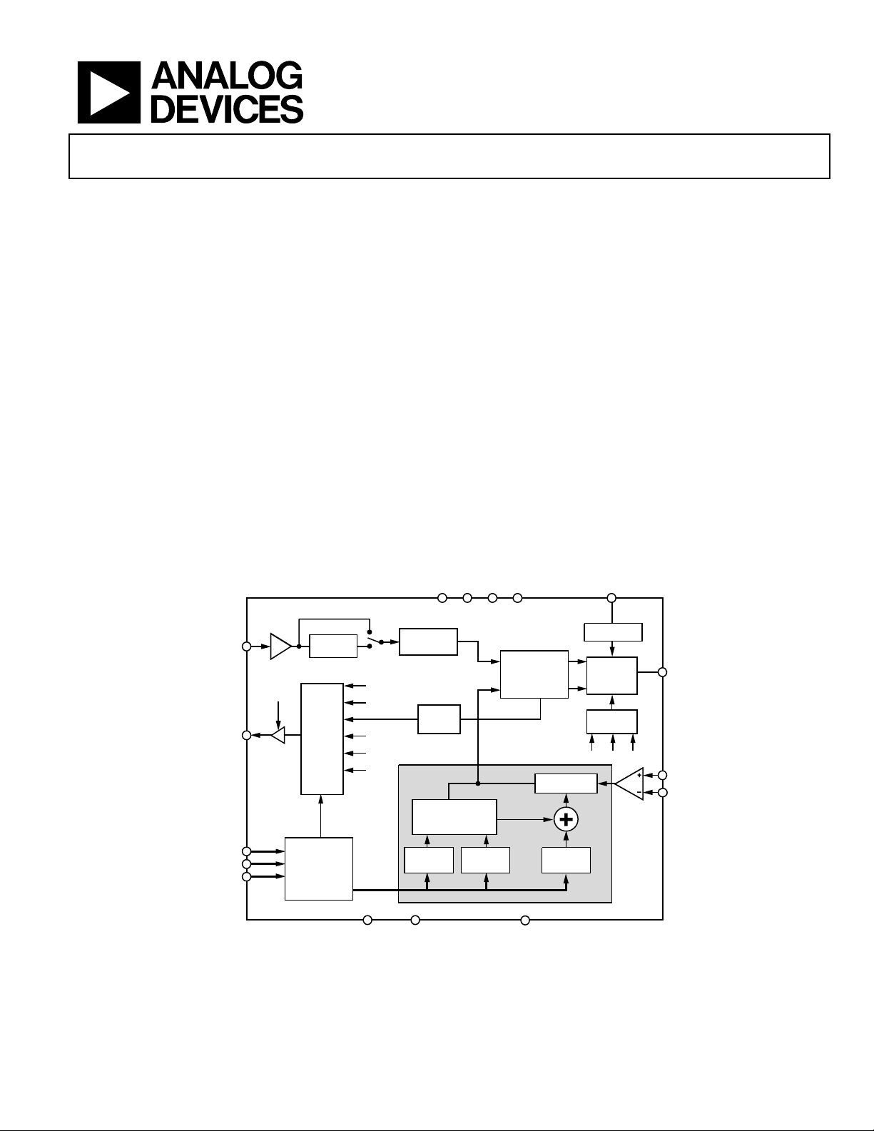
FUNCTIONAL BLOCK DIAGRAM
×2
DOUBLER
MUX
V
DD
DGND
V
DD
R
DIV
N
DIV
AV
DD
4-BIT
R COUNTER
LOCK
DETECT
THIRD ORDER
FRACTIONAL
INTERPOLATOR
FRACTION
REG
ADF4153
GENERAL DESCRIPTION
The ADF4153 is a fractional-N frequency synthesizer that
implements local oscillators in the upconversion and
downconversion sections of wireless receivers and transmitters.
It consists of a low noise digital phase frequency detector
(PFD), a precision charge pump, and a programmable reference
divider. There is a Σ-Δ based fractional interpolator to allow
programmable fractional-N division. The INT, FRAC, and
MOD registers define an overall N divider (N = (INT +
(FRAC/MOD))). In addition, the 4-bit reference counter (R
counter) allows selectable REFIN frequencies at the PFD input.
A complete phase-locked loop (PLL) can be implemented if the
synthesizer is used with an external loop filter and a voltage
controlled oscillator (VCO).
Control of all on-chip registers is via a simple 3-wire interface.
The device operate with a power supply ranging from 2.7 V to
3.3 V and can be powered down when not in use.
DV
DDVP
MODULUS
REG
SDV
DD
+
PHASE
FREQUENCY
DETECTOR
–
N-COUNTER
INTEGER
REG
R
SET
REFERENCE
CHARGE
PUMP
CURRENT
SETTING
RFCP3 RFCP2 RFCP1
CP
RFINA
RF
IN
B
AGND
Rev. A
Information furnished by Analog Devices is believed to be accurate and reliable.
However, no responsibility is assumed by Analog Devices for its use, nor for any
infringements of patents or other rights of third parties that may result from its use.
Specifications subject to change without notice. No license is granted by implication
or otherwise under any patent or patent rights of Analog Devices. Trademarks and
registered trademarks are the property of their respective owners.
DGND CPGND
Figure 1.
03685-A-001
One Technology Way, P.O. Box 9106, Norwood, MA 02062-9106, U.S.A.
Tel: 781.329.4700 www.analog.com
Fax: 781.326.8703 © 2004 Analog Devices, Inc. All rights reserved.
Page 2

ADF4153
TABLE OF CONTENTS
Specifications..................................................................................... 3
R Divider Register, R1................................................................ 17
Timing Characteristics..................................................................... 5
Absolute Maximum Ratings............................................................ 6
ESD Caution.................................................................................. 6
Pin Configuration and Pin Function Descriptions...................... 7
Typical Performance Characteristics ............................................. 8
Circuit Description......................................................................... 10
Reference Input Section............................................................. 10
RF Input Stage............................................................................. 10
RF INT Divider........................................................................... 10
INT, FRAC, MOD, and R Relationship.................................... 10
RF R COUNTER ........................................................................10
Phase Frequency Detector (PFD) and Charge Pump............ 11
MUXOUT and LOCK Detect................................................... 11
Input Shift Registers................................................................... 11
Program Modes .......................................................................... 11
Control Register, R2................................................................... 17
Noise and Spur Register, R3 ...................................................... 18
Reserved Bits............................................................................... 18
RF Synthesizer: A Worked Example ........................................ 18
Modulus....................................................................................... 19
Reference Doubler and Reference Divider ............................. 19
12-Bit Programmable Modulus................................................ 19
Spurious Optimization and Fastlock ....................................... 19
Phase Resync and Spur Consistency ....................................... 19
Spurious Signals—Predicting Where They Will Appear....... 20
Filter Design—ADIsimPLL....................................................... 20
Interfacing ................................................................................... 20
PCB Design Guidelines for Chip Scale Package .................... 21
Outline Dimensions....................................................................... 22
Ordering Guide .......................................................................... 22
N Divider Register, R0 ............................................................... 17
REVISION HISTORY
1/04—Data Sheet Changed from a REV. 0 to a REV. A
Renumbered Figures and Tables.............................. UNIVERSAL
Changes to Specifications............................................................... 3
Changes to Pin Function Description ..........................................7
Changes to RF Power-Down section ..........................................17
Changes to PCB Design Guidelines for Chip Scale
Package section .............................................................................. 21
Updated Outline Dimensions...................................................... 22
Updated Ordering Guide.............................................................. 22
7/03—Revision 0: Initial Version
Rev. A | Page 2 of 24
Page 3

ADF4153
SPECIFICATIONS1
AVDD = DVDD = SDVDD = 2.7 V to 3.3 V; VP = AVDD to 5.5 V; AGND = DGND = 0 V; TA = T
referred to 50 Ω.
Table 1.
Parameter B Version Unit Test Conditions/Comments
RF CHARACTERISTICS (3 V)
RF Input Frequency (RFIN)2 0.5/4.0 GHz min/max
1.0/4.0 GHz min/max −10 dBm/0 dBm min/max.
REFERENCE CHARACTERISTICS See Figure 16 for input circuit.
REFIN Input Frequency2 10/250 MHz min/max
REFIN Input Sensitivity 0.7/AVDD V p-p min/max AC-coupled.
0 to AVDD V max CMOS compatible.
REFIN Input Capacitance 10 pF max
REFIN Input Current ±100 µA max
PHASE DETECTOR
Phase Detector Frequency3 32 MHz max
CHARGE PUMP
ICP Sink/Source Programmable. See Table 5.
High Value 5 mA typ With R
Low Value 312.5 µA typ
Absolute Accuracy 2.5 % typ With R
R
Range 1.5/10 kΩ min/max
SET
ICP Three-State Leakage Current 1 nA typ Sink and source current.
Matching 2 % typ 0.5 V < VCP < VP – 0.5.
ICP vs. VCP 2 % typ 0.5 V < VCP < VP – 0.5.
ICP vs. Temperature 2 % typ VCP = VP/2.
LOGIC INPUTS
V
, Input High Voltage 1.4 V min
INH
V
, Input Low Voltage 0.6 V max
INL
I
, Input Current ±1 µA max
INH/IINL
CIN, Input Capacitance 10 pF max
LOGIC OUTPUTS
VOH, Output High Voltage 1.4 V min Open-drain 1 kΩ pull-up to 1.8 V.
VOL, Output Low Voltage 0.4 V max IOL = 500 µA.
POWER SUPPLIES
AVDD 2.7/3.3 V min/V max
DVDD, SDVDD AVDD
VP AVDD/5.5 V min/V max
4
I
24 mA max 20 mA typical.
DD
Low Power Sleep Mode 1 µA typ
NOISE CHARACTERISTICS
Phase Noise Figure of Merit5 −217 dBc/Hz typ
ADF4153 Phase Noise Floor6 −147 dBc/Hz typ @ 10 MHz PFD frequency.
−143 dBc/Hz typ @ 26 MHz PFD frequency.
Phase Noise Performance7 @ VCO output.
1750 MHz Output8 −106 dBc/Hz typ @ 1 kHz offset, 26 MHz PFD frequency.
See footnotes on next page.
MIN
to T
, unless other wise noted; dBm
MAX
See Figure 17 for input circuit.
−8 dBm/0 dBm min/max. For lower frequencies,
ensure slew rate (SR) > 396 V/µs.
For f < 10 MHz, use a dc-coupled CMOS compatible
square wave, slew rate > 21 V/µs.
= 5.1 kΩ.
SET
= 5.1 kΩ.
SET
Rev. A | Page 3 of 24
Page 4

ADF4153
1
Operating temperature is B version: −40°C to +80°C.
2
Use a square wave for frequencies below f
3
Guaranteed by design. Sample tested to ensure compliance.
4
AC coupling ensures AVDD/2 bias. See Figure 16 for typical circuit.
5
This figure can be used to calculate phase noise for any application. Use the formula –217 + 10log(f
at the VCO output. The value given is the lowest noise mode.
6
The synthesizer phase noise floor is estimated by measuring the in-band phase noise at the output of the VCO and subtracting 20logN (where N is the N divider value).
The value given is the lowest noise mode.
7
The phase noise is measured with the EVAL-ADF4153EB1 evaluation board and the HP8562E spectrum analyzer.
8
f
= 26 MHz; f
REFIN
= 10 MHz; offset frequency = 1 kHz; RF
PFD
.
MIN
) + 20logN to calculate in-band phase noise performance as seen
PFD
= 1750 MHz; N = 175; loop B/W = 20 kHz; lowest noise mode.
OUT
Rev. A | Page 4 of 24
Page 5
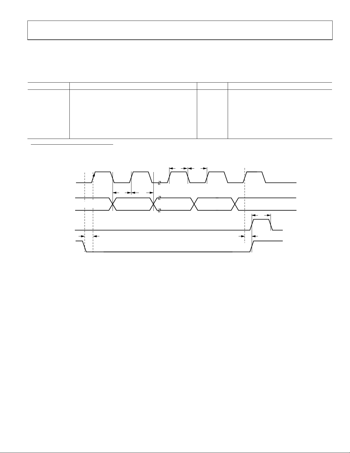
ADF4153
K
TIMING CHARACTERISTICS1
AVDD = DVDD = SDVDD = 2.7 V to 3.3 V; VP = AVDD to 5.5 V; AGND = DGND = 0 V; TA = T
referred to 50 Ω.
Table 2.
Parameter Limit at T
MIN
to T
(B Version) Unit Test Conditions/Comments
MAX
t1 20 ns min LE Setup Time
t2 10 ns min DATA to CLOCK Setup Time
t3 10 ns min DATA to CLOCK Hold Time
t4 25 ns min CLOCK High Duration
t5 25 ns min CLOCK Low Duration
t6 10 ns min CLOCK to LE Setup Time
t7 20 ns min LE Pulse Width
1
Guaranteed by design but not production tested.
CLOC
t
4
t
5
MIN
to T
, unless other wise noted; dBm
MAX
DATA
t
2
DB23 (MSB) DB22 DB2
LE
t
1
LE
t
3
DB1
(CONTROL BIT C2)
DB0 (LSB)
(CONTROL BIT C1)
t
7
t
6
04414-0-002
Figure 2. Timing Diagram
Rev. A | Page 5 of 24
Page 6

ADF4153
ABSOLUTE MAXIMUM RATINGS1, 2, 3, 4
TA = 25°C, unless otherwise noted.
Table 3.
Parameter Rating
VDD to GND −0.3 V to +4 V
VDD to VDD −0.3 V to +0.3 V
VP to GND −0.3 V to +5.8 V
VP to VDD −0.3 V to +5.8 V
Digital I/O Voltage to GND −0.3 V to VDD + 0.3 V
Analog I/O Voltage to GND −0.3 V to VDD + 0.3 V
REFIN, RFIN to GND −0.3 V to VDD + 0.3 V
Operating Temperature Range
Industrial (B Version) −40°C to +85°C
Storage Temperature Range −65°C to +150°C
Maximum Junction Temperature 150°C
TSSOP θJA Thermal Impedance 150.4°C/W
LFCSP θJA Thermal Impedance (Paddle Soldered) 122°C/W
LFCSP θJA Thermal Impedance (Paddle Not Soldered) 216°C/W
Lead Temperature, Soldering
Vapor Phase (60 sec) 215°C
Infrared 220°C
1
Stresses above those listed under Absolute Maximum Ratings may cause permanent damage to the device. This is a stress rating only; functional operation of the
device at these or any other conditions above those listed in the operational sections of this specification is not implied. Exposure to absolute maximum rating
conditions for extended periods may affect device reliability.
2
This device is a high performance RF integrated circuit with an ESD rating of < 2 kV, and it is ESD sensitive. Proper precautions should be taken for handling and
assembly.
3
GND = AGND = DGND = 0 V.
4
VDD = AVDD = DVDD = SDVDD.
ESD CAUTION
ESD (electrostatic discharge) sensitive device. Electrostatic charges as high as 4000 V readily accumulate on the
human body and test equipment and can discharge without detection. Although this product features
proprietary ESD protection circuitry, permanent damage may occur on devices subjected to high energy
electrostatic discharges. Therefore, proper ESD precautions are recommended to avoid performance
degradation or loss of functionality.
Rev. A | Page 6 of 24
Page 7
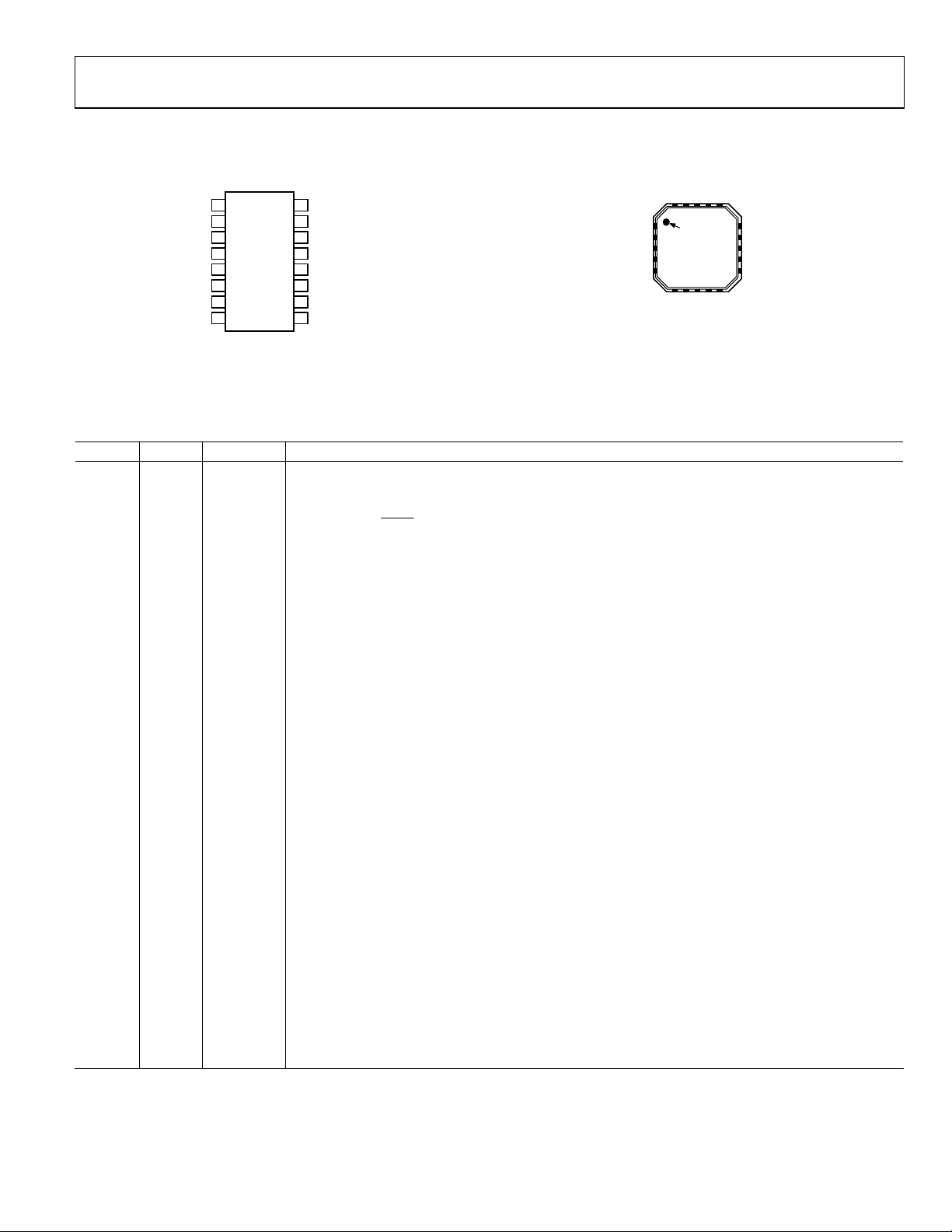
ADF4153
D
D
PIN CONFIGURATION AND PIN FUNCTION DESCRIPTIONS
D
1
R
SET
CP
2
CPGND
3
DD
IN
ADF4153
4
TOP VIEW
5
(Not to Scale)
6
7
8
AGND
RFINB
RFIINA
AV
REF
Figure 3. TSSOP Pin Configuration
16
15
14
13
12
11
10
9
V
P
DV
DD
MUXOUT
LE
DATA
CLK
SDV
DD
DGND
CPGND 1
AGND 2
AGND 3
RFINB4
RF
A5
IN
03685-A-002
Figure 4. LFCSP Pin Configuration
CP
201917
ADF4153
TOP VIEW
6
AV
Table 4. Pin Function Descriptions
TSSOP LFCSP Mnemonic Description
1 19 R
2 20 CP
SET
Connecting a resistor between this pin and ground sets the maximum charge pump output current.
= 5 mA.
and R
CP
The relation ship between I
525I.
=
CP
max
R
SET
With R
= 5.1 kΩ, I
SET
CPmax
Charge Pump Output. When enabled, this provides ±I
SET
is
to the external loop filter, which in turn drives
CP
the external VCO.
3 1 CPGND Charge Pump Ground. This is the ground return path for the charge pump.
4 2, 3 AGND Analog Ground. This is the ground return path of the prescaler.
5 4 RFINB
Complementary Input to the RF Prescaler. This point should be decoupled to the ground plane with a
small bypass capacitor, typically 100 pF (see Figure 17).
6 5 RFINA Input to the RF Prescaler. This small-signal input is normally ac-coupled from the VCO.
7 6, 7 AVDD
8 8 REFIN
Positive Power Supply for the RF Section. Decoupling capacitors to the digital ground plane should be
placed as close as possible to this pin. AV
as DV
.
DD
has a value of 3 V ± 10%. AVDD must have the same voltage
DD
Reference Input. This is a CMOS input with a nominal threshold of V
resistance of 100 kΩ (see Figure 16). This input can be driven from a TTL or CMOS crystal oscillator, or it
can be ac-coupled.
9 9, 10 DGND Digital Ground.
10 11 SDVDD
11 12 CLK
∑-∆ Power. Decoupling capacitors to the digital ground plane should be placed as close as possible to
this pin. SDV
has a value of 3 V ± 10%. SDVDD must have the same voltage as DVDD.
DD
Serial Clock Input. This serial clock is used to clock in the serial data to the registers. The data is latched
into the shift register on the CLK rising edge. This input is a high impedance CMOS input.
12 13 DATA
Serial Data Input. The serial data is loaded MSB first with the two LSBs being the control bits. This input
is a high impedance CMOS input.
13 14 LE
Load Enable, CMOS Input. When LE is high, the data stored in the shift registers is loaded into one of
the four latches, the latch being selected using the control bits.
14 15 MUXOUT
This multiplexer output allows either the RF lock detect, the scaled RF, or the scaled reference
frequency to be accessed externally.
15 16, 17 DVDD
Positive Power Supply for the Digital Section. Decoupling capacitors to the digital ground plane should
be placed as close as possible to this pin. DVDD has a value of 3 V ± 10%. DVDD must have the same
.
DD
16 18 VP
voltage as AV
Charge Pump Power Supply. This should be greater than or equal to V
can be set to 5.5 V and used to drive a VCO with a tuning range of up to 5.5 V.
D
SET
R
VPDV
DV
191817
16
16
PIN 1
INDICATOR
7
8
IN
DD
DD
AV
REF
DGND 9
MUXOUT
15
LE
14
DATA
13
CLK
12
SDV
11
DD
DGND 10
03685-A-003
/2 and an equivalent input
DD
. In systems where VDD is 3 V, it
DD
Rev. A | Page 7 of 24
Page 8
ADF4153
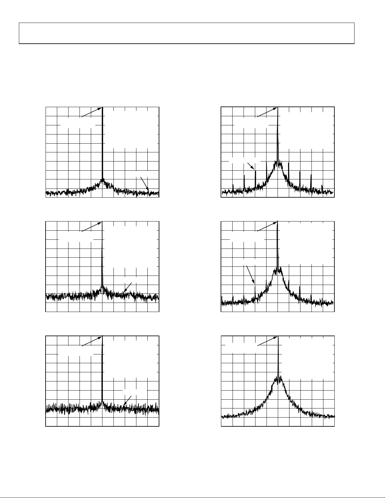
TYPICAL PERFORMANCE CHARACTERISTICS
Figure 5 to Figure 10: RF
= 5 mA.
and I
CP
Loop Bandwidth = 20 kHz, Reference = Fox 10 MHz TCXO, VCO = Vari-L VCO190-1750T, Eval Board = Eval-ADF4153EB1,
measurements taken on HP8562E spectrum analyzer.
0
–10
–20
–30
–40
–50
–60
–70
OUTPUT POWER (dB)
–80
–90
–100
–10
–20
–30
–40
–50
–60
–70
OUTPUT POWER (dB)
–80
–90
–100
–10
–20
–30
–40
–50
–60
–70
OUTPUT POWER (dB)
–80
–90
–100
0
0
REFERENCE
LEVEL = –4dBm
–2kHz –1kHz 1kHz 2kHz1.722GHz
Figure 5. Phase Noise (Lowest Noise Mode)
REFERENCE
LEVEL = –4.2dBm
–2kHz –1kHz 1kHz 2kHz1.722GHz
Figure 6. Phase Noise (Low Noise Mode and Spur Mode)
REFERENCE
LEVEL = –4.2dBm
–2kHz –1kHz 1kHz 2kHz1.722GHz
Figure 7. Phase Noise (Lowest Spur Mode)
= 1.722 GHz, PFD Freq = 26 MHz, INT = 66, Channel Spacing = 200 kHz, Modulus = 130, Fraction = 1/130,
OUT
0
VDD = 3V, VP = 5V
= 5mA
I
CP
PFD FREQUENCY = 26MHz
CHANNEL STEP = 200kHz
LOOP BANDWIDTH = 20kHz
LOWEST NOISE MODE
N = 66 1/130
RBW = 10Hz
–102dBc/Hz
–10
–20
–30
–40
–50
–60
–70
OUTPUT POWER (dB)
–80
–90
03685-A-004
–100
REFERENCE
LEVEL = –4.2dBm
–71dBc@200kHz
–400kHz –200kHz 200kHz 400kHz1.722GHz
VDD = 3V, VP = 5V
= 5mA
I
CP
PFD FREQUENCY = 26MHz
CHANNEL STEP = 200kHz
LOOP BANDWIDTH = 20kHz
LOWEST NOISE MODE
N = 66 1/130
RBW = 10Hz
Figure 8. Spurs (Lowest Noise Mode)
VDD = 3V, VP = 5V
= 5mA
I
CP
PFD FREQUENCY = 26MHz
CHANNEL STEP = 200kHz
LOOP BANDWIDTH = 20kHz
LOW NOISE AND
SPUR MODE
N = 66 1/130
RBW = 10Hz
–95dBc/Hz
0
–10
REFERENCE
LEVEL = –4.2dBm
–20
–30
–40
–50
–60
–70
OUTPUT POWER (dB)
–80
–90
03685-A-005
–100
–74dBc@200kHz
–400kHz –200kHz 200kHz 400kHz1.722GHz
VDD = 3V, VP = 5V
= 5mA
I
CP
PFD FREQUENCY = 26MHz
CHANNEL STEP = 200kHz
LOOP BANDWIDTH = 20kHz
LOW NOISE AND
SPUR MODE
N = 66 1/130
RBW = 10Hz
Figure 9. Spurs (Low Noise and Spur Mode)
VDD = 3V, VP = 5V
= 5mA
I
CP
PFD FREQUENCY = 26MHz
CHANNEL STEP = 200kHz
LOOP BANDWIDTH = 20kHz
LOWEST SPUR MODE
N = 66 1/130
RBW = 10Hz
–90dBc/Hz
0
–10
REFERENCE
LEVEL = –4.2dBm
–20
–30
–40
–50
–60
–70
OUTPUT POWER (dB)
–80
–90
03685-A-006
–100
–400kHz –200kHz 200kHz 400kHz1.722GHz
VDD = 3V, VP = 5V
= 5mA
I
CP
PFD FREQUENCY = 26MHz
CHANNEL STEP = 200kHz
LOOP BANDWIDTH = 20kHz
LOWEST SPUR NOISE
N = 66 1/130
RBW = 10Hz
Figure 10. Spurs (Lowest Spur Mode)
03685-A-007
03685-A-008
03685-A-009
Rev. A | Page 8 of 24
Page 9

ADF4153
–130
–140
–80
–85
–90
–150
PHASE NOISE (dBc/Hz)
–160
–170
100 1000 10000 100000
PHASE DETECTOR FREQUENCY (kHz)
Figure 11. PFD Noise Floor vs. PFD Frequency (Lowest Noise Mode)
5
0
–5
–10
–15
–20
AMPLITUDE (dBm)
–25
–30
–35
0 0.5 1.0 1.5 4.03.53.02.52.0 4.5
FREQUENCY (GHz)
P = 4/5
P = 8/9
Figure 12. RF Input Sensitivity
6
5
4
3
2
1
0
(mA)
–1
CP
I
–2
–3
–4
–5
–6
012345
VCP(V)
Figure 13. Charge Pump Output Characteristics
–95
–100
PHASE NOISE (dBc/Hz)
–105
03685-A-010
03685-A-011
PHASE NOISE (dBc/Hz)
–110
–90
–92
–94
–96
–98
–100
–102
–104
–60 100–40
03530252015105
R
VALUE (kΩ)
SET
Figure 14. Phase Noise vs. R
–20 0 20 40 60
TEMPERATURE(°C)
SET
80
03685-A-013
03685-A-014
Figure 15. Phase Noise vs. Temperature
03685-A-012
Rev. A | Page 9 of 24
Page 10

ADF4153
()(
)
+×=
(
)
+×=
CIRCUIT DESCRIPTION
REFERENCE INPUT SECTION
The reference input stage is shown in Figure 16. SW1 and SW2
are normally closed switches. SW3 is normally open. When
power-down is initiated, SW3 is closed and SW1 and SW2 are
opened. This ensures that there is no loading of the REF
on power-down.
POWER-DOWN
CONTROL
IN
pin
INT, FRAC, MOD, AND R RELATIONSHIP
The INT, FRAC, and MOD values, in conjunction with the
R counter, make it possible to generate output frequencies that
are spaced by fractions of the phase frequency detector (PFD).
See the RF Synthesizer: A Worked Example section for more
information. The RF VCO frequency (RF
PFD
OUT
) equation is
OUT
MODFRACINTFRF
(1)
100kΩ
NC
SW1
SW2
SW3
NO
REF
IN
NC
Figure 16. Reference Input Stage
BUFFER
TO R COUNTER
04414-0-010
RF INPUT STAGE
The RF input stage is shown in Figure 17. It is followed by a
2-stage limiting amplifier to generate the current mode logic
(CML) clock levels needed for the prescaler.
BIAS
GENERATOR
A
RF
IN
B
RF
IN
1.6V
2kΩ 2kΩ
AV
DD
where
RF
is the output frequency of external voltage
OUT
controlled oscillator (VCO).
RDREFF
1 (2)
INPFD
where:
REF
is the reference input frequency.
IN
D is the REF
doubler bit.
IN
R is the preset divide ratio of binary 4-bit programmable
reference counter (1 to 15).
INT is the preset divide ratio of binary 9-bit counter (31 to 511).
MOD is the preset modulus ratio of binary 12-bit
programmable FRAC counter (2 to 4095).
FRAC is the preset fractional ratio of binary 12-bit
programmable FRAC counter (0 to MOD).
RF R COUNTER
The 4-bit RF R counter allows the input reference frequency
(REF
) to be divided down to produce the reference clock to
IN
the PFD. Division ratios from 1 to 15 are allowed.
AGND
Figure 17. RF Input Stage
03685-A-015
RF INT DIVIDER
The RF INT CMOS counter allows a division ratio in the PLL
feedback counter. Division ratios from 31 to 511 are allowed.
FROM RF
INPUT STAGE
RF N DIVIDER
N-COUNTER
INT
REG
Figure 18. A and B Counters
N = INT + FRAC/MOD
THIRD ORDER
FRACTIONAL
INTERPOLATOR
MOD
REG
FRAC
VALUE
TO PFD
03685-A-016
Rev. A | Page 10 of 24
Page 11

ADF4153
+
PHASE FREQUENCY DETECTOR (PFD) AND CHARGE PUMP
The PFD takes inputs from the R counter and N counter and
produces an output proportional to the phase and frequency
difference between them. Figure 19 is a simplified schematic.
The PFD includes a fixed delay element that sets the width of
the antibacklash pulse, which is typically 3 ns. This pulse
ensures that there is no dead zone in the PFD transfer function,
and gives a consistent reference spur level.
HI
IN
HI
–IN
UP
Q1D1
U1
CLR1
DELAY
CLR2
DOWN
Q2D2
U2
Figure 19. PFD Simplified Schematic
U3
CHARGE
PUMP
CP
03685-A-017
MUXOUT AND LOCK DETECT
The output multiplexer on the ADF4153 allows the user to
access various internal points on the chip. The state of
MUXOUT is controlled by M3, M2, and M1 (see Table 8).
Figure 20 shows the MUXOUT section in block diagram form.
The N-channel open-drain analog lock detect should be
operated with an external pull-up resistor of 10 kΩ nominal.
When lock has been detected, it is high with narrow low-going
pulses.
DV
DD
INPUT SHIFT REGISTERS
The ADF4153 digital section includes a 4-bit RF R counter, a 9bit RF N counter, a 12-bit FRAC counter, and a 12-bit modulus
counter. Data is clocked into the 24-bit shift register on each
rising edge of CLK. The data is clocked in MSB first. Data is
transferred from the shift register to one of four latches on the
rising edge of LE. The destination latch is determined by the
state of the two control bits (C2 and C1) in the shift register.
These are the 2 LSBs, DB1 and DB0, as shown in Figure 2. The
truth table for these bits is shown in Table 5. Table 6 shows a
summary of how the latches are programmed.
PROGRAM MODES
Table 5 through Table 10 show how to set up the program
modes in the ADF4153.
The ADF4153 programmable modulus is double buffered. This
means that two events have to occur before the part uses a new
modulus value. First, the new modulus value is latched into the
device by writing to the R divider register. Second, a new write
must be performed on the N divider register. Therefore, any
time that the modulus value has been updated, the N divider
register must be written to after this, to ensure that the modulus
value is loaded correctly.
Table 5. C2 and C1 Truth Table
Control Bits
C2 C1 Register
0 0 N Divider Register
0 1 R Divider Register
1 0 Control Register
1 1 Noise and Spur Register
THREE-STATE OUTPUT
LOGIC LOW
DIGITAL LOCK DETECT
R COUNTER OUTPUT
N COUNTER OUTPUT
ANALOG LOCK DETECT
LOGIC HIGH
CONTROLMUX
Figure 20. MUXOUT Schematic
DGND
MUXOUT
03685-A-018
Rev. A | Page 11 of 24
Page 12

ADF4153
Table 6. Register Summary
N DIVIDER REG
FASTLOCK
DB23 DB22 DB21
FL1
LOAD
DB23 DB22 DB21
MUXOUT
CONTROL
9-BIT INTEGER VALUE (INT)
DB20 DB19 DB18 DB17 DB16 DB15 DB14 DB13 DB12 DB11 DB10 DB9 DB8 DB7 DB6 DB5 DB4 DB3 DB2 DB1 DB0
M2M3P3
N7N8N9
DB20 DB19
P2
RESERVED
PRESCALER
DB18 DB17 DB16 DB15 DB14 DB13 DB12 DB11 DB10 DB9 DB8 DB7 DB6 DB5 DB4 DB3 DB2 DB1 DB0
P1M1
N2
4-BIT
R COUNTER
R2
DB15
RESYNC
DB14 DB13 DB12 DB11 DB10 DB9 DB8 DB7 DB6 DB5 DB4 DB3 DB2 DB1 DB0
12-BIT FRACTIONAL VALUE (FRAC)
12-BIT INTERPOLATOR MODULUS VALUE (MOD)
M1M2M3M4M5M6M7M8M9M10M11M12R1R3R4
CP CURRENT
SETTING
CP/2
DOUBLER
REFERENCE
CP3
NOISE AND SPUR
RESERVED
DB10 DB9 DB8 DB7 DB6 DB5 DB4 DB3 DB1 DB0
T9
MODE
LDP
PD POLARITY
RESERVED
POWER-
CP
DOWN
THREE-STATE
U1U2U3U4U5CP0CP1CP2U6S1S2S3S4
NOISE AND SPUR REG
NOISE
DB2
T1T2T3T4T5T6T7T8
COUNTER
RESET
AND SPUR
CONTROL
BITS
C2 (0) C1 (0)F1F2F3F4F5F6F7F8F9F10F11F12N1N3N4N5N6
R DIVIDER REG
CONTROL
BITS
C2 (0) C1 (1)
CONTROL REG
CONTROL
BITS
C2 (1) C1 (0)
CONTROL
BITS
MODE
C2 (1) C1 (1)
03685-A-019
Rev. A | Page 12 of 24
Page 13

ADF4153
Table 7. N Divider Register Map
FAST LOCK
DB23 DB22
N9
FL1
9-BIT INTEGER VALUE (INT)
DB21
DB20 DB19 DB18 DB17 DB16 DB15 DB14 DB13 DB12 DB11 DB10 DB9 DB8 DB7 DB6 DB5 DB4 DB3 DB2 DB1 DB0
N8
N7
N9 N8 N7 N6 N5 N4 N3 N2 N1 INTEGER VALUE (INT)
000 1131
0
001 0032
0
001 0133
0
001 0034
0
... ...
.
... ...
.
... ...
.
1 1 1 1 1 509
1
1 1 1 1 0 510
1
1
111
N2
N1N3N4N5N6
F12 F11 F10 F3 F2 F1 FRACTIONAL VALUE (FRAC)
0 .......... 0
0 .......... 0
0 .......... 0
0 .......... 0
. .......... .
. .......... .
. .......... .
1 .......... 1 4092
1 .......... 1 4093
1 .......... 1 4094
1
0
0
0
0
.
.
.
1
1
1
1
1
0
0
0
.
.
.
1
1
1
1
0
0
0
.
.
...
1
1
11
0
0
0
0
.
.
.
1
1
1
1
12-BIT FRACTIONAL VALUE (FRAC)
F8
F9F10F11F12
0
0
1
1
.
.
.
0
0
1
1
1
0
0
1
.
.
.
0
1
1 1 511
0
1
0
1
.
.
.
0
1
0
1.......... 1 4095
CONTROL
BITS
C2 (0) C1 (0)
F1F2F3F4F5F6F7
0
1
2
3
.
.
.
FL1 FASTLOCK
0 NORMAL OPERATION
1 FAST LOCK ENABLED
Rev. A | Page 13 of 24
03685-A-020
Page 14

ADF4153
Table 8. R Divider Register Map
MUXOUT
LOAD
CONTROL
DB23 DB22 DB21
P3
P3 LOAD CONTROL
0 NORMAL OPERATION
1 LOAD RESYNC
M2M3
RESERVED
DB20 DB19
DB18 DB17 DB16 DB15 DB14 DB13 DB12 DB11 DB10 DB9 DB8 DB7 DB6 DB5 DB4 DB3 DB2 DB1 DB0
P2
P1 PRESCALER
0 4/5
1 8/9
12-BIT INTERPOLATOR MODULUS VALUE (MOD)4-BIT R COUNTER
PRESCALER
P1M1
R4 R3 R2 R1
0
0
0
0
.
.
.
112
113
114
1
R2
M12
0 0 .......... 0 1 0 2
0 0 .......... 0 1 1 3
0 0 .......... 1 0 0 4
. . .......... . . . .
. . .......... . . . .
. . .......... . . . .
1 1 .......... 1 0 0 4092
1 1 .......... 1 0 1 4093
1 1 .......... 1 1 0 4094
1
0
0
1
0
1
0
0
1
.
.
.
.
.
.
0
1
0
1
1
1
1
1
M11 M10 M3 M2 M1
0
0
0
.
.
.
1
1
1
1 1 .......... 1 1 1 4095
RF R COUNTER
DIVIDE RATIO
1
1
2
0
3
1
4
0
.
.
.
.
.
.
0
1
0
115
CONTROL
BITS
M1M2M3M4M5M6M7M8M9M10M11M12R1R3R4
C2 (0) C1 (1)
INTERPOLATOR
MODULUS VALUE (MOD)
M3 M2 M1 MUXOUT
0
0
0 THREE-STATE OUTPUT
0
0 N DIVIDER OUTPUT
0
1 R DIVIDER OUTPUT
1
1 FASTLOCK SWITCH
1
1
0
1
1
0
0
1
1
DIGITAL LOCK DETECT
0
1
LOGIC HIGH
0
1
ANALOG LOCK DETECT
0
1
LOGIC LOW
03685-A-021
Rev. A | Page 14 of 24
Page 15

ADF4153
Table 9. Control Register Map
CP3
CP/2
CP CURRENT
SETTING
I
(mA)
CP
RESYNC
DOUBLE
REFERENCE
DB14 DB13 DB12 DB11 DB10 DB9 DB8 DB7 DB6 DB5 DB4 DB3 DB2 DB1 DB0
DB15
REFERENCE
U6
DOUBLER
0 DISABLED
1 ENABLED
S4 S3 S2 S1 RESYNC
011
002
013
...
...
...
1113
1014
1
CP3 CP2 CP1 CP0 2.7kΩ 5.1kΩ 10kΩ
0 1.09 0.63 0.29
0 2.18 1.25 0.59
0 3.26 1.88 0.88
0 4.35 2.50 1.15
0 5.44 3.13 1.47
0 6.53 3.75 1.76
0 7.62 4.38 2.06
0 8.70 5.00 2.35
1 0.54 0.31 0.15
1 1.10 0.63 0.30
1 1.64 0.94 0.44
1 2.18 1.25 0.588
1 2.73 1.57 0.74
1 3.27 1.88 0.88
1 3.81 2.19 1.03
1
0
0
0
.
.
.
1
1
1
0
0
0
0
1
1
1
1
0
0
0
0
1
1
1
1
0
1
1
.
.
.
0
1
1115
0
0
1
1
0
0
1
1
0
0
1
1
0
0
1
1
0
1
0
1
0
1
0
1
0
1
0
1
0
1
0
1 4.35 2.50 1.18
LDP
DOWN
PD POLARITY
U5 PD POLARITY
0 NEGATIVE
1 POSITIVE
POWER-
U3 POWER-DOWN
0 NORMAL OPERATION
1 POWER-DOWN
U4 LDP
013
5
CP
THREE-STATE
U2 CP THREE-STATE
0 DISABLED
1 THREE-STATE
CONTROL
BITS
RESET
COUNTER
C2 (1) C1 (0)
U1U2U3U4U5CP0CP1CP2U6S1S2S3S4
U1 COUNTER RESET
0 DISABLED
ENABLED1
03685-A-022
Rev. A | Page 15 of 24
Page 16

ADF4153
Table 10. Noise and Spur Register
NOISE AND SPUR
RESERVED
DB10 DB9 DB8 DB7 DB6 DB5 DB4 DB3 DB1
T9
MODE
NOISE AND SPUR SETTINGDB9, DB8, DB7, DB6, DB2
LOWEST SPUR MODE00000
LOW NOISE AND SPUR MODE11100
LOWEST NOISE MODE11111
RESERVED
THESE BITS MUST BE SET TO 0
FOR NORMAL OPERATION.
NOISE
DB2
T1T2T3T4T5T6T7T8
AND SPUR
MODE
RESERVEDDB10, DB5, DB4, DB3
RESERVED0
CONTROL
BITS
C2 (1)
DB0
C1 (1)
03685-A-023
Rev. A | Page 16 of 24
Page 17

ADF4153
N DIVIDER REGISTER, R0
With R0[1, 0] set to [0, 0], the on-chip N divider register is
programmed. Table 7 shows the input data format for
programming this register.
9-Bit INT Value
These nine bits control what is loaded as the INT value. This is
used to determine the overall feedback division factor. It is used
in Equation 1.
12-Bit FRAC Value
These 12 bits control what is loaded as the FRAC value into the
fractional interpolator. This is part of what determines the
overall feedback division factor. It is used in Equation 1. The
FRAC value must be less than or equal to the value loaded into
the MOD register.
Fastlock
When set to logic high, this enables the fastlock. This sets the
charge pump current to its maximum value. When set to logic
low, the charge pump current is equal to the value programmed
in the function register.
R DIVIDER REGISTER, R1
With R1[1, 0] set to [0, 1], the on-chip R divider register is
programmed. Table 8 shows the input data format for
programming this register.
Load Control
When set to logic high, the value being programmed in the
modulus is not loaded into the modulus. Instead, it sets the
resync delay of the Σ-Δ. This is done to ensure phase resync
when changing frequencies. See the Phase Resync and Spur
Consistency section for more information and a worked
example.
MUXOUT
The on-chip multiplexer is controlled by R1[22 ... 20] on the
ADF4153. Table 8 shows the truth table.
Digital Lock Detect
The digital lock detect output goes high if there are 40
successive PFD cycles with an input error of less than 15 ns. It
stays high until a new channel is programmed or until the error
at the PFD input exceeds 30 ns for one or more cycles. If the
loop bandwidth is narrow compared to the PFD frequency, the
error at the PFD inputs may drop below 15 ns for 40 cycles
around a cycle slip. Therefore, the digital lock detect may go
falsely high for a short period until the error again exceeds
30 ns. In this case, the digital lock detect is reliable only as a
loss-of-lock detector.
Prescaler (P/P + 1)
The dual-modulus prescaler (P/P + 1), along with the INT,
FRAC, and MOD counters, determines the overall division ratio
from the RF
to the PFD input. Operating at CML levels, it
IN
takes the clock from the RF input stage and divides it down for
the counters. It is based on a synchronous 4/5 core. When set to
4/5, the maximum RF frequency allowed is 2 GHz. Therefore,
when operating the ADF4153 above 2 GHz, this must be set to
8/9. The prescaler limits the INT value.
With P = 4/5, N
With P = 8/9, N
MIN
MIN
= 31.
= 91.
The prescaler can also influence the phase noise performance. If
INT < 91, a prescaler of 4/5 should be used. For applications
where INT > 91, P = 8/9 should be used for optimum noise
performance (see Table 8).
4-Bit RF R Counter
The 4-bit RF R counter allows the input reference frequency
(REF
) to be divided down to produce the reference clock to
IN
the phase frequency detector (PFD). Division ratios from 1 to
15 are allowed.
12-Bit Interpolator Modulus
This programmable register sets the fractional modulus. This is
the ratio of the PFD frequency to the channel step resolution on
the RF output. Refer to the RF Synthesizer: A Worked Example
section for more information.
The ADF4153 programmable modulus is double buffered. This
means that two events have to occur before the part uses a new
modulus value. First, the new modulus value is latched into the
device by writing to the R divider register. Second, a new write
must be performed on the N divider register. Therefore, any
time that the modulus value has been updated, the N divider
register must be written to after this, to ensure that the modulus
value is loaded correctly.
CONTROL REGISTER, R2
With R2[1, 0] set to [0, 1], the on-chip control register is
programmed. Table 9 shows the input data format for
programming this register.
RF Counter Reset
DB3 is the RF counter reset bit for the ADF4153. When this is 1,
the RF synthesizer counters are held in reset. For normal
operation, this bit should be 0.
RF Charge Pump Three-State
This bit puts the charge pump into three-state mode when
programmed to 1. It should be set to 0 for normal operation.
RF Power-Down
DB4 on the ADF4153 provides the programmable power-down
mode. Setting this bit to 1 performs a power-down. Setting this
bit to 0 returns the synthesizer to normal operation. While in
software power-down mode, the part retains all information in
its registers. Only when supplies are removed are the register
contents lost.
Rev. A | Page 17 of 24
Page 18

ADF4153
(
)
[
]
+
=
(
)
[
]
+×=
When a power-down is activated, the following events occur:
1. All active dc current paths are removed.
2. The synthesizer counters are forced to their load state
conditions.
3. The charge pump is forced into three-state mode.
4. The digital lock detect circuitry is reset.
5. The RF
6. The input register remains active and capable of loading
and latching data.
Lock Detect Precision (LDP)
When this bit is programmed to 0, three consecutive reference
cycles of 15 ns must occur before digital lock detect is set. When
this bit is programmed to 1, five consecutive reference cycles of
15 ns must occur before digital lock detect is set.
Phase Detector Polarity
DB6 in the ADF4153 sets the phase detector polarity. When the
VCO characteristics are positive, this should be set to 1. When
they are negative, it should be set to 0.
Charge Pump Current Setting
DB7, DB8, and DB9 set the charge pump current setting. This
should be set to the charge pump current that the loop filter is
designed with (see Table 9).
REFIN Doubler
Setting this bit to 0 feeds the REFIN signal directly to the 4-bit
RF R counter, disabling the doubler. Setting this bit to 1
multiplies the REF
into the 4-bit R counter. When the doubler is disabled, the REF
falling edge is the active edge at the PFD input to the fractional
synthesizer. When the doubler is enabled, both the rising and
falling edges of REF
When the doubler is enabled and the lowest spur mode is
chosen, the in-band phase noise performance is sensitive to the
REF
IN
as 5 dB for the REF
The phase noise is insensitive to the REF
lowest noise mode and in the lowest noise and spur mode. The
phase noise is insensitive to REF
is disabled.
NOISE AND SPUR REGISTER, R3
With R3[1, 0] set to 1, 1, the on-chip noise and spur register is
programmed. Table 10 shows the input data format for
programming this register.
Noise and Spur Mode
Noise and spur mode allows the user to optimize a design either
for improved spurious performance or for improved phase
noise performance. When the lowest spur setting is chosen,
input is debiased.
IN
frequency by a factor of 2 before feeding
IN
become active edges at the PFD input.
IN
duty cycle. The phase noise degradation can be as much
duty cycles outside a 45% to 55% range.
IN
duty cycle in the
IN
duty cycle when the doubler
IN
dither is enabled. This randomizes the fractional quantization
noise so that it looks more like white noise rather than spurious
noise. This means that the part is optimized for improved
spurious performance. This operation would normally be used
when the PLL closed-loop bandwidth is wide, for fast-locking
applications. (Wide-loop bandwidth is seen as a loop bandwidth
greater than 1/10 of the RF
wide-loop filter does not attenuate the spurs to a level that a
narrow-loop bandwidth would. When the low noise and spur
setting is enabled, dither is disabled. This optimizes the
synthesizer to operate with improved noise performance.
However, the spurious performance is degraded in this mode
compared to the lowest spurs setting. To further improve noise
performance, the lowest noise setting option can be used, which
reduces the phase noise. As well as disabling the dither, it also
ensures that the charge pump is operating in an optimum
region for noise performance. This setting is extremely useful
where a narrow-loop filter bandwidth is available. The
synthesizer ensures extremely low noise and the filter attenuates
the spurs. The typical performance characteristics give the user
an idea of the trade-off in a typical WCDMA setup for the
different noise and spur settings.
channel step resolution (f
OUT
RES
)). A
RESERVED BITS
These bits should be set to 0 for normal operation.
RF SYNTHESIZER: A WORKED EXAMPLE
This equation governs how the synthesizer should be
programmed.
[]
FMODFRACINTRF ×
(3)
OUT
IN
where:
RF
is the RF frequency output.
OUT
INT is the integer division factor.
FRAC is the fractionality.
MOD is the modulus.
RDREFF
1 (4)
INPFD
where:
REFIN is the reference frequency input.
D is the RF REF
R is the RF reference division factor.
doubler bit.
IN
PFD
Rev. A | Page 18 of 24
Page 19

ADF4153
(
)
[
]
(
)
Example: In a GSM 1800 system, where 1.8 GHz RF frequency
output (RF
(REF
IN
required on the RF output.
From Equation 4:
) is required, a 13 MHz reference frequency input
OUT
) is available and a 200 kHz channel resolution (f
=
PFD
fREFMOD
IN
RES
kHzMHzMOD
30;138
=≥=
FRACINT
6520013 ==
MHzMHzF
1310113 =+×= (5)
65138.1
FRACINTMHzG
≥+×=
(6)
RES
) is
MODULUS
The choice of modulus (MOD) depends on the reference signal
(REF
) available and the channel resolution (f
IN
the RF output. For example, a GSM system with 13 MHz REF
would set the modulus to 65. This means that the RF output
resolution (f
) is the 200 kHz (13 MHz/65) necessary for GSM.
RES
) required at
RES
IN
REFERENCE DOUBLER AND REFERENCE DIVIDER
The reference doubler on-chip allows the input reference signal
to be doubled. This is useful for increasing the PFD comparison
frequency. Making the PFD frequency higher improves the
noise performance of the system. Doubling the PFD frequency
usually results in an improvement in noise performance of 3 dB.
It is important to note that the PFD cannot be operated above
32 MHz due to a limitation in the speed of the Σ-Δ circuit of
the N divider.
12-BIT PROGRAMMABLE MODULUS
Unlike most other fractional-N PLLs, the ADF4153 allows the
user to program the modulus over a 12-bit range. This means
that the user can set up the part in many different
configurations for the application, when combined with the
reference doubler and the 4-bit R counter.
For example, here is an application that requires 1.75 GHz RF
and 200 kHz channel step resolution. The system has a 13 MHz
reference signal.
One possible setup is feeding the 13 MHz directly to the PFD
and programming the modulus to divide by 65. This would
result in the required 200 kHz resolution.
benefit. PDC requires 25 kHz channel step resolution, whereas
GSM 1800 requires 200 kHz channel step resolution. A 13 MHz
reference signal could be fed directly to the PFD. The modulus
would be programmed to 520 when in PDC mode (13 MHz/
520 = 25 kHz). The modulus would be reprogrammed to 65 for
GSM 1800 operation (13 MHz/65 = 200 kHz). It is important
that the PFD frequency remains constant (13 MHz). This allows
the user to design one loop filter that can be used in both setups
without running into stability issues. It is the ratio of the RF
frequency to the PFD frequency that affects the loop design.
Keeping this relationship constant, instead of changing the
modulus factor, results in a stable filter.
SPURIOUS OPTIMIZATION AND FASTLOCK
As mentioned earlier, the part can be optimized for spurious
performance. However, in fast locking applications, the loop
bandwidth needs to be wide, and therefore the filter does not
provide much attenuation of the spurs. The programmable
charge pump can be used to get around this issue. The filter is
designed for a narrow-loop bandwidth so that steady-state
spurious specifications are met. This is designed using the
lowest charge pump current setting. To implement fastlock
during a frequency jump, the charge pump current is set to the
maximum setting for the duration of the jump. This has the
effect of widening the loop bandwidth, which improves lock
time. When the PLL has locked to the new frequency, the charge
pump is again programmed to the lowest charge pump current
setting. This narrows the loop bandwidth to its original cutoff
frequency to allow better attenuation of the spurs than the
wide-loop bandwidth.
PHASE RESYNC AND SPUR CONSISTENCY
Setting the RESYNC bits [S4 ,S3, S2, and S1] enables the phase
RESYNC feature. With a fractional denominator of MOD, a
fractional-N PLL can settle with any one of (2 × π)/MOD valid
phase offsets with respect to the reference input. This is
different from integer-N where the RF output always settles to
the same static phase offset with respect to the input reference,
which is zero ideally. This is not an issue in applications that
require only a consistent frequency lock. When RESYNC is
enabled, it also ensures that spur levels remain consistent when
the PLL returns to a certain frequency. This is due to the fact
that the RESYNC function resets the Σ-Δ modulator. RESYNC
is enabled by setting the S4 to S1 bits in R2 to a nonzero value.
When the S4 to S1 bits are 0, 0, 0, and 0, RESYNC is disabled.
Another possible setup is using the reference doubler to create
26 MHz from the 13 MHz input signal. This 26 MHz is then fed
into the PFD. The modulus is now programmed to divide by
130. This also results in 200 kHz resolution and offers superior
phase noise performance over the previous setup.
The programmable modulus is also very useful for multistandard applications. If a dual-mode phone requires PDC and
GSM 1800 standards, the programmable modulus is a huge
Rev. A | Page 19 of 24
For applications where a consistent phase relationship between
the output and reference is required (i.e., digital beam forming),
the ADF4153 can be used with the phase resync feature enabled.
This ensures that if the user programs the PLL to jump from
Frequency (and Phase) A to Frequency (and Phase) B and back
again to Frequency A, the PLL returns to the original phase
(Phase A).
Page 20

ADF4153
When enabled, it activates every time the user programs
Register R0 to set a new output frequency. However, if a cycle
slip occurs in the settling transient after the phase RESYNC
operation, the phase RESYNC is lost. This can be avoided by
delaying the RESYNC activation until the locking transient is
close to its final frequency. This is done by rewriting to R1 after
R1 has been set up as normal. Setting load control [DB23]
allows this. When set, instead of determining the fractional
denominator, the MOD bits [M12 to M1] are used to set a time
interval from when the new channel is programmed to the time
the RESYNC is activated. This is called the delay. Its value
should be programmed to set a time interval that is at least as
long as the RF PLL lock time.
For example, if REF
200 kHz output steps (f
time of 150 µs, then delay should be programmed to 3,900,
as 26 MHz × 150 µs = 3,900.
If the application requires the delay to be greater than 4095, the
RESYNC bits should be increased. For example, if the lock time
above is 1.5 ms, the delay should be programmed to 26 MHz ×
1.5 ms = 39,000. In this case, program M12 to M1 to 3,900 and
program S4 to S1 to 10. The delay is 3,900 × 10 = 39,000.
SPURIOUS SIGNALS—PREDICTING WHERE THEY WILL APPEAR
Just as in integer-N PLLs, spurs appear at PFD frequency offsets
from the carrier. In a fractional-N PLL, spurs also appear at
frequencies equal to the RF
The third-order fractional interpolator engine of the ADF4153
may also introduce subfractional spurs. If the fractional
denominator (MOD) is divisible by 2, spurs appear at 1/2 f
the fractional denominator (MOD) is divisible by 3, spurs
appear at 1/3 f
appear. With the lowest spur mode enabled, the fractional and
subfractional spurs is attenuated dramatically. The worst-case
spurs appear when the fraction is programmed to (1/MOD).
For example, in a GSM 900 MHz system with a 26 MHz PFD
frequency and an RF
kHz, the MOD = 130. PFD spurs appear at 26 MHz offset, and
fractional spurs appear at 200 kHz offset. Since MOD is
divisible by 2, subfractional spurs are also present at 100 kHz
offset.
= 26 MHz and MOD = 130 to give
IN
), and the RF loop has a settling
RES
channel step resolution (f
OUT
Harmonics of all spurs mentioned will also
RES.
channel step resolution (f
OUT
) of 200
RES
RES
).
RES.
If
INTERFACING
The ADF4153 has a simple SPI® compatible serial interface for
writing to the device. SCLK, SDATA, and LE control the data
transfer. When LE (latch enable) is high, the 22 bits that have
been clocked into the input register on each rising edge of
SCLK are transferred to the appropriate latch. See Figure 2 for
the timing diagram and Table 5 for the latch truth table.
The maximum allowable serial clock rate is 20 MHz. This
means that the maximum update rate possible for the device is
909 kHz or one update every 1.1 µs. This is more than adequate
for systems that have typical lock times in the hundreds of
microseconds.
ADuC812 Interface
Figure 21 shows the interface between the ADF4153 and the
ADuC812 MicroConverter®. Since the ADuC812 is based on an
8051 core, this interface can be used with any 8051-based
microcontroller. The MicroConverter is set up for SPI master
mode with CPHA = 0. To initiate the operation, the I/O port
driving LE is brought low. Each latch of the ADF4153 needs a
24-bit word, which is accomplished by writing three 8-bit bytes
from the MicroConverter to the device. After the third byte is
written, the LE input should be brought high to complete the
transfer.
When operating in the mode described, the maximum
SCLOCK rate of the ADuC812 is 4 MHz. This means that the
maximum rate at which the output frequency can be changed is
180 kHz.
ADuC812 ADF4153
SCLOCK
MOSI
I/O PORTS
Figure 21. ADuC812 to ADF4153 Interface
SCLK
SDATA
LE
MUXOUT
(LOCK DETECT)
03685-A-024
FILTER DESIGN—ADISIMPLL
A filter design and analysis program is available to help the user
to implement PLL design. Visit www.analog.com/pll for a free
download of the ADIsimPLL software. The software designs,
simulates, and analyzes the entire PLL frequency domain and
time domain response. Various passive and active filter
architectures are allowed. REV. #2 of ADIsimPLL allows analysis
of the ADF4153.
Rev. A | Page 20 of 24
Page 21

ADF4153
ADSP-2181 Interface
Figure 22 shows the interface between the ADF4153 and the
ADSP-21xx digital signal processor. As discussed previously, the
ADF4153 needs a 24-bit serial word for each latch write. The
easiest way to accomplish this using the ADSP-21xx family is to
use the autobuffered transmit mode of operation with alternate
framing. This provides a means for transmitting an entire block
of serial data before an interrupt is generated. Set up the word
length for eight bits and use three memory locations for each
24-bit word. To program each 24-bit latch, store the three 8-bit
bytes, enable the autobuffered mode, and write to the transmit
register of the DSP. This last operation initiates the autobuffer
transfer.
ADSP-21xx ADF4153
SCLOCK
DT
TFS
SCLK
SDATA
LE
PCB DESIGN GUIDELINES FOR CHIP SCALE PACKAGE
The lands on the chip scale package (CP-20) are rectangular.
The printed circuit board pad for these should be 0.1 mm
longer than the package land length and 0.05 mm wider than
the package land width. The land should be centered on the pad.
This ensures that the solder joint size is maximized.
The bottom of the chip scale package has a central thermal pad.
The thermal pad on the printed circuit board should be at least
as large as this exposed pad. On the printed circuit board, there
should be a clearance of at least 0.25 mm between the thermal
pad and the inner edges of the pad pattern. This ensures that
shorting is avoided.
Thermal vias may be used on the printed circuit board thermal
pad to improve thermal performance of the package. If vias are
used, they should be incorporated in the thermal pad at 1.2 mm
pitch grid. The via diameter should be between 0.3 mm and
0.33 mm, and the via barrel should be plated with 1 oz. copper
to plug the via.
I/O FLAGS
Figure 22. ADSP-21xx to ADF4153 Interface
MUXOUT
(LOCK DETECT)
03685-A-025
The user should connect the printed circuit board thermal pad
to AGND.
Rev. A | Page 21 of 24
Page 22

ADF4153
OUTLINE DIMENSIONS
5.10
5.00
4.90
0.15
0.05
PIN 1
INDICATOR
1.00
0.85
0.80
SEATING
PLANE
4.50
4.40
4.30
PIN 1
16
0.65
BSC
COPLANARITY
9
6.40
BSC
81
1.20 MAX
0.30
0.19
0.10
COMPLIANT TO JEDEC STANDARDS MO-153AB
SEATING
PLANE
0.20
0.09
8°
0°
Figure 23. 16-Lead Thin Shrink Small Outline Package [TSSOP]
(RU-16)
Dimensions shown in millimeters
0.60
MAX
0.60
MAX
0.75
0.55
0.35
COPLANARITY
0.08
16
15
11
10
BOTTOM
VIEW
0.30
0.23
0.18
12° MAX
BSC SQ
0.50
BSC
4.0
TOP
VIEW
0.80 MAX
0.65 TYP
0.20
REF
3.75
BSC SQ
0.05 MAX
0.02 NOM
0.75
0.60
0.45
20
1
2.25
2.10 SQ
1.95
5
6
0.25MIN
COMPLIANT TO JEDEC STANDARDS MO-220-VGGD-1
Figure 24. 20-Lead Lead Frame Chip Scale Package [LFCSP]
4 mm × 4 mm Body
(CP-20)
Dimensions shown in millimeters
ORDERING GUIDE
Model Description Temperature Range Package Option
ADF4153BRU Thin Shrink Small Outline Package (TSSOP) −40°C to +85°C RU-16
ADF4153BRU-REEL Thin Shrink Small Outline Package (TSSOP) −40°C to +85°C RU-16
ADF4153BRU-REEL7 Thin Shrink Small Outline Package (TSSOP) −40°C to +85°C RU-16
ADF4153BCP Lead Frame Chip Scale Package (LFCSP) −40°C to +85°C CP-20
ADF4153BCP-REEL Lead Frame Chip Scale Package (LFCSP) −40°C to +85°C CP-20
ADF4153BCP-REEL7 Lead Frame Chip Scale Package (LFCSP) −40°C to +85°C CP-20
EVAL-ADF4153EB1 Evaluation Board
Rev. A | Page 22 of 24
Page 23

ADF4153
NOTES
Rev. A | Page 23 of 24
Page 24

ADF4153
NOTES
Purchase of licensed I2C components of Analog Devices or one of its sublicensed Associated Companies conveys a license for the purchaser under the Philips I2C Patent
Rights to use these components in an I
2
C system, provided that the system conforms to the I2C Standard Specification as defined by Philips.
© 2004 Analog Devices, Inc. All rights reserved. Trademarks and
registered trademarks are the property of their respective owners.
C03685–0–1/04(A)
Rev. A | Page 24 of 24
 Loading...