

Page 1
RF PLL Frequency Synthesizers
FEATURES
ADF4110: 550 MHz; ADF4111: 1.2 GHz; ADF4112: 3.0 GHz;
ADF4113: 4.0 GHz
2.7 V to 5.5 V power supply
Separate charge pump supply (V
voltage in 3 V systems
Programmable dual-modulus prescaler 8/9, 16/17, 32/33,
64/65
Programmable charge pump currents
Programmable antibacklash pulse width
3-wire serial interface
Analog and digital lock detect
Hardware and software power-down mode
APPLICATIONS
Base stations for wireless radio (GSM, PCS, DCS, CDMA,
WCDMA)
Wireless handsets (GSM, PCS, DCS, CDMA, WCDMA)
Wireless LANS
Communications test equipment
CATV equipment
) allows extended tuning
P
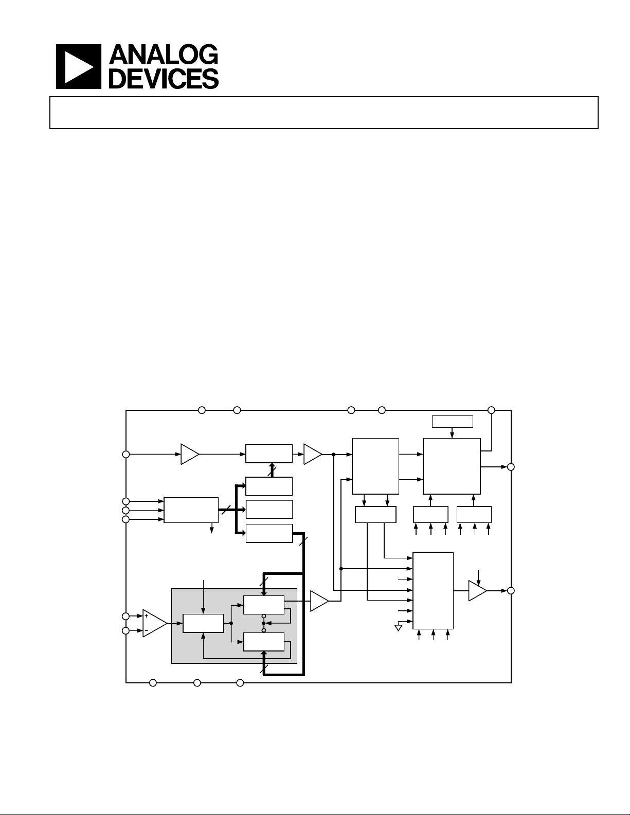
FUNCTIONAL BLOCK DIAGRAM
AV
DV
DD
DD
ADF4110/ADF4111/ADF4112/ADF4113
GENERAL DESCRIPTION
The ADF4110 family of frequency synthesizers can be used to
implement local oscillators in the upconversion and downconversion sections of wireless receivers and transmitters. They
consist of a low noise digital PFD (phase frequency detector), a
precision charge pump, a programmable reference divider,
programmable A and B counters, and a dual-modulus prescaler
(P/P + 1). The A (6-bit) and B (13-bit) counters, in conjunction
with the dual-modulus prescaler (P/P + 1), implement an N
divider (N = BP + A). In addition, the 14-bit reference counter
(R counter) allows selectable REFIN frequencies at the PFD
input. A complete phase-locked loop (PLL) can be implemented
if the synthesizer is used with an external loop filter and voltage
controlled oscillator (VCO).
Control of all the on-chip registers is via a simple 3-wire
interface. The devices operate with a power supply ranging from
2.7 V to 5.5 V and can be powered down when not in use.
V
CPGND
P
R
SET
REF
CLK
DATA
LE
RF
IN
RF
IN
IN
24-BIT
INPUT REGISTER
FUNCTION
LATCH
A
B
PRESCALER
SD
FROM
P/P +1
22
OUT
N = BP + A
R COUNTER
R COUNTER
A, B COUNTER
B COUNTER
LOAD
LOAD
A COUNTER
DGNDAGNDCE
14-BIT
14
LATCH
FUNCTION
LATCH
LATCH
13
13-BIT
6-BIT
6
Figure 1. Functional Block Diagram
Rev. C
Information furnished by Analog Devices is believed to be accurate and reliable.
However, no responsibility is assumed by Analog Devices for its use, nor for any
infringements of patents or other rights of third parties that may result from its use.
Specifications subject to change without notice. No license is granted by implication
or otherwise under any patent or patent rights of Analog Devices. Trademarks and
registered trademarks are the property of their respective owners.
19
ADF4110/ADF4111
ADF4112/ADF4113
REFERENCE
PHASE
FREQUENCY
DETECTOR
LOCK
DETECT
AV
SD
OUT
CPI3 CPI2 CPI1 CPI6 CPI5 CPI4
DD
CHARGE
PUMP
CURRENT
SETTING 1
MUX
M3 M2 M1
CURRENT
SETTING 2
HIGH Z
CP
MUXOUT
03496-0-001
One Technology Way, P.O. Box 9106, Norwood, MA 02062-9106, U.S.A.
Tel: 781.329.4700
www.analog.com
Fax: 781.326.8703 © 2004 Analog Devices, Inc. All rights reserved.
Page 2

ADF4110/ADF4111/ADF4112/ADF4113
TABLE OF CONTENTS
Specifications..................................................................................... 3
Input Shift Register .................................................................... 13
Timing Characteristics..................................................................... 5
Absolute Maximum Ratings............................................................ 6
Transistor Count........................................................................... 6
ESD Caution.................................................................................. 6
Pin Configurations and Function Descriptions ........................... 7
Typical Performance Characteristics ............................................. 8
Circuit Description......................................................................... 12
Reference Input Section............................................................. 12
RF Input Stage............................................................................. 12
Prescaler (P/P + 1)...................................................................... 12
A and B Counters ....................................................................... 12
R Counter ....................................................................................12
Phase Frequency Detector (PFD) and Charge Pump............ 13
Muxout and Lock Detect........................................................... 13
Function Latch............................................................................ 19
Initialization Latch..................................................................... 20
Device Programming after Initial Power-Up ......................... 20
Resynchronizing the Prescaler Output.................................... 21
Applications..................................................................................... 22
Local Oscillator for GSM Base Station Transmitter .............. 22
Using a D/A Converter to Drive the R
Shutdown Circuit ....................................................................... 23
Wideband PLL............................................................................ 23
Direct Conversion Modulator .................................................. 25
Interfacing ................................................................................... 26
PCB Design Guidelines for Chip Scale Package .................... 26
Outline Dimensions....................................................................... 27
Ordering Guide............................................................................... 28
Pin......................... 23
SET
REVISION HISTORY
3/04—Data sheet changed from Rev. B to Rev. C.
Updated Format..............................................................Universal
Changes to Specifications............................................................ 2
Changes to Figure 32.................................................................. 22
Changes to the Ordering Guide................................................ 28
3/03—Data sheet changed from Rev. A to Rev. B.
Edits to Specifications.................................................................. 2
Updated OUTLINE DIMENSIONS ........................................ 24
1/01—Data sheet changed from Rev. 0 to Rev. A.
Changes to DC Specifications in B Version, B Chips,
Unit, and Test Conditions/Comments Columns................. 2
Changes to Absolute Maximum Rating..................................... 4
Changes to FR
Changes to Figure 8...................................................................... 7
New Graph Added—TPC 22....................................................... 9
Change to PD Polarity Box in Table V..................................... 15
Change to PD Polarity Box in Table VI................................... 16
Change to PD Polarity Paragraph ............................................17
Addition of New Material
(PCB Design Guidelines for Chip–Scale package) ........... 23
Replacement of CP-20 Outline with CP-20 [2] Outline........ 24
A Function Test ................................................ 5
IN
Rev. C | Page 2 of 28
Page 3

ADF4110/ADF4111/ADF4112/ADF4113
SPECIFICATIONS
AVDD = DVDD = 3 V ± 10%, 5 V ± 10%; AVDD ≤VP ≤ 6.0 V; AGND = DGND = CPGND = 0 V; R
to T
T
MIN
, unless otherwise noted. Operating temperature range is as follows: B Version: −40°C to +85°C.
MAX
Table 1.
Parameter B Version B Chips1 Unit Test Conditions/Comments
RF CHARACTERISTICS (3 V) See Figure 29 for input circuit.
RF Input Sensitivity −15/0 −15/0 dBm min/max
RF Input Frequency
ADF4110 80/550 80/550 MHz min/max For lower frequencies, ensure slew rate
ADF4110 50/550 50/550 MHz min/max Input level = −10 dBm.
ADF4111 0.08/1.2 0.08/1.2 GHz min/max For lower frequencies, ensure SR > 30 V/µs.
ADF4112 0.2/3.0 0.2/3.0 GHz min/max For lower frequencies, ensure SR > 75 V/µs.
ADF4112 0.1/3.0 0.1/3.0 GHz min/max Input level = −10 dBm.
ADF4113 0.2/3.7 0.2/3.7 GHz min/max Input level = −10 dBm. For lower frequencies,
Maximum Allowable Prescaler Output
Frequency
2
165 165 MHz max
RF CHARACTERISTICS (5 V)
RF Input Sensitivity −10/0 −10/0 dBm min/max
RF Input Frequency
ADF4110 80/550 80/550 MHz min/max For lower frequencies, ensure SR > 50 V/µs.
ADF4111 0.08/1.4 0.08/1.4 GHz min/max For lower frequencies, ensure SR > 50 V/µs.
ADF4112 0.1/3.0 0.1/3.0 GHz min/max For lower frequencies, ensure SR > 75 V/µs.
ADF4113 0.2/3.7 0.2/3.7 GHz min/max For lower frequencies, ensure SR > 130 V/µs.
ADF4113 0.2/4.0 0.2/4.0 GHz min/max Input level = −5 dBm
Maximum Allowable Prescaler Output
Frequency
2
200 200 MHz max
REFIN CHARACTERISTICS
REFIN Input Frequency 5/104 5/104 MHz min/max For f < 5 MHz, ensure SR > 100 V/µs.
Reference Input Sensitivity 0.4/AVDD 0.4/AVDD V p-p min/max AVDD = 3.3 V, biased at AVDD/2. See Note 3.
3.0/AVDD 3.0/AVDD V p-p min/max AVDD = 5 V, biased at AVDD/2. See Note 3.
REFIN Input Capacitance 10 10 pF max
REFIN Input Current ±100 ±100 µA max
PHASE DETECTOR FREQUENCY4 55 55 MHz max
CHARGE PUMP
ICP Sink/Source Programmable (see Table 9).
High Value 5 5 mA typ With R
Low Value 625 625 µA typ
Absolute Accuracy 2.5 2.5 % typ With R
R
Range 2.7/10 2.7/10 kΩ typ See Table 9.
SET
ICP 3-State Leakage Current 1 1 nA typ
Sink and Source Current Matching 2 2 % typ 0.5 V ≤ VCP ≤ VP – 0.5 V.
ICP vs. VCP 1.5 1.5 % typ 0.5 V ≤ VCP ≤ VP – 0.5 V.
ICP vs. Temperature 2 2 % typ VCP = VP/2.
LOGIC INPUTS
V
, Input High Voltage 0.8 × DVDD 0.8 × DVDD V min
INH
V
, Input Low Voltage 0.2 × DVDD 0.2 × DVDD V max
INL
I
, Input Current ±1 ±1 µA max
INH/IINL
CIN, Input Capacitance 10 10 pF max
LOGIC OUTPUTS
VOH, Output High Voltage DVDD – 0.4 DVDD – 0.4 V min IOH = 500 µA.
VOL, Output Low Voltage 0.4 0.4 V max IOL = 500 µA.
(SR) > 30 V/µs.
ensure SR > 130 V/µs.
= 4.7 kΩ; dBm referred to 50 Ω; TA =
SET
= 4.7 kΩ
SET
= 4.7 kΩ
SET
Rev. C | Page 3 of 28
Page 4

ADF4110/ADF4111/ADF4112/ADF4113
Parameter B Version B Chips1 Unit Test Conditions/Comments
POWER SUPPLIES
AVDD 2.7/5.5 2.7/5.5 V min/V max
DV
AVDD AVDD
DD
VP AVDD/6.0 AVDD/6.0 V min/V max AVDD ≤ VP ≤ 6.0 V. See Figure 25 and Figure 26.
5
I
(AIDD + DIDD)
DD
ADF4110 5.5 4.5 mA max 4.5 mA typical
ADF4111 5.5 4.5 mA max 4.5 mA typical
ADF4112 7.5 6.5 mA max 6.5 mA typical
ADF4113 11 8.5 mA max 8.5 mA typical
IP 0.5 0.5 mA max TA = 25°C
Low Power Sleep Mode 1 1 µA typ
NOISE CHARACTERISTICS
ADF4113 Normalized Phase Noise Floor6 −215 −215 dBc/Hz typ
Phase Noise Performance7 @ VCO output
ADF4110: 540 MHz Output8 −91 −91 dBc/Hz typ @ 1 kHz offset and 200 kHz PFD frequency
ADF4111: 900 MHz Output9 −87 −87 dBc/Hz typ @ 1 kHz offset and 200 kHz PFD frequency
ADF4112: 900 MHz Output9 −90 −90 dBc/Hz typ @ 1 kHz offset and 200 kHz PFD frequency
ADF4113: 900 MHz Output9 −91 −91 dBc/Hz typ @ 1 kHz offset and 200 kHz PFD frequency
ADF4111: 836 MHz Output10 −78 −78 dBc/Hz typ @ 300 Hz offset and 30 kHz PFD frequency
ADF4112: 1750 MHz Output11 −86 −86 dBc/Hz typ @ 1 kHz offset and 200 kHz PFD frequency
ADF4112: 1750 MHz Output12 −66 −66 dBc/Hz typ @ 200 Hz offset and 10 kHz PFD frequency
ADF4112: 1960 MHz Output13 −84 −84 dBc/Hz typ @ 1 kHz offset and 200 kHz PFD frequency
ADF4113: 1960 MHz Output13 −85 −85 dBc/Hz typ @ 1 kHz offset and 200 kHz PFD frequency
ADF4113: 3100 MHz Output
Spurious Signals
ADF4110: 540 MHz Output9 −97/−106 −97/−106 dBc typ @ 200 kHz/400 kHz and 200 kHz PFD frequency
ADF4111: 900 MHz Output9 −98/−110 −98/−110 dBc typ @ 200 kHz/400 kHz and 200 kHz PFD frequency
ADF4112: 900 MHz Output9 −91/−100 −91/−100 dBc typ @ 200 kHz/400 kHz and 200 kHz PFD frequency
ADF4113: 900 MHz Output9 −100/−110 −100/−110 dBc typ @ 200 kHz/400 kHz and 200 kHz PFD frequency
ADF4111: 836 MHz Output10 −81/−84 −81/−84 dBc typ @ 30 kHz/60 kHz and 30 kHz PFD frequency
ADF4112: 1750 MHz Output11 −88/−90 −88/−90 dBc typ @ 200 kHz/400 kHz and 200 kHz PFD frequency
ADF4112: 1750 MHz Output12 −65/−73 −65/−73 dBc typ @ 10 kHz/20 kHz and 10 kHz PFD frequency
ADF4112: 1960 MHz Output13 −80/−84 −80/−84 dBc typ @ 200 kHz/400 kHz and 200 kHz PFD frequency
ADF4113: 1960 MHz Output13 −80/−84 −80/−84 dBc typ @ 200 kHz/400 kHz and 200 kHz PFD frequency
ADF4113: 3100 MHz Output14 −80/−82 −82/−82 dBc typ @ 1 MHz/2 MHz and 1 MHz PFD frequency
1
The B chip specifications are given as typical values.
2
This is the maximum operating frequency of the CMOS counters. The prescaler value should be chosen to ensure that the RF input is divided down to a frequency that
is less than this value.
3
AC coupling ensures AVDD/2 bias. See Figure 33 for a typical circuit.
4
Guaranteed by design.
5
TA = 25°C; AVDD = DVDD = 3 V; P = 16; SYNC = 0; DLY = 0; RFIN for ADF4110 = 540 MHz; RFIN for ADF4111, ADF4112, ADF4113 = 900 MHz.
6
The synthesizer phase noise floor is estimated by measuring the in-band phase noise at the output of the VCO, PN
value) and 10logF
7
The phase noise is measured with the EVAL-ADF411xEB1 evaluation board and the HP8562E spectrum analyzer. The spectrum analyzer provides the REFIN for the
synthesizer (f
8
f
= 10 MHz; f
REFIN
9
f
= 10 MHz; f
REFIN
10
f
= 10 MHz; f
REFIN
11
f
= 10 MHz; f
REFIN
12
f
= 10 MHz; f
REFIN
13
f
= 10 MHz; f
REFIN
14
f
= 10 MHz; f
REFIN
: PN
PFD
SYNTH
= 10 MHz @ 0 dBm). SYNC = 0; DLY = 0 (Ta ). ble 7
REFOUT
= 200 kHz; offset frequency = 1 kHz; fRF = 540 MHz; N = 2700; loop B/W = 20 kHz.
PFD
= 200 kHz; offset frequency = 1 kHz; fRF = 900 MHz; N = 4500; loop B/W = 20 kHz.
PFD
= 30 kHz; offset frequency = 300 Hz; fRF = 836 MHz; N = 27867; loop B/W = 3 kHz.
PFD
= 200 kHz; offset frequency = 1 kHz; fRF = 1750 MHz; N = 8750; loop B/W = 20 kHz
PFD
= 10 kHz; offset frequency = 200 Hz; fRF = 1750 MHz; N = 175000; loop B/W = 1 kHz.
PFD
= 200 kHz; offset frequency = 1 kHz; fRF = 1960 MHz; N = 9800; loop B/W = 20 kHz.
PFD
= 1 MHz; offset frequency = 1 kHz; fRF = 3100 MHz; N = 3100; loop B/W = 20 kHz.
PFD
= PN
14
−86 −86 dBc/Hz typ @ 1 kHz offset and 1 MHz PFD frequency
, and subtracting 20logN (where N is the N divider
– 10logF
TOT
– 20logN.
PFD
TOT
Rev. C | Page 4 of 28
Page 5
ADF4110/ADF4111/ADF4112/ADF4113
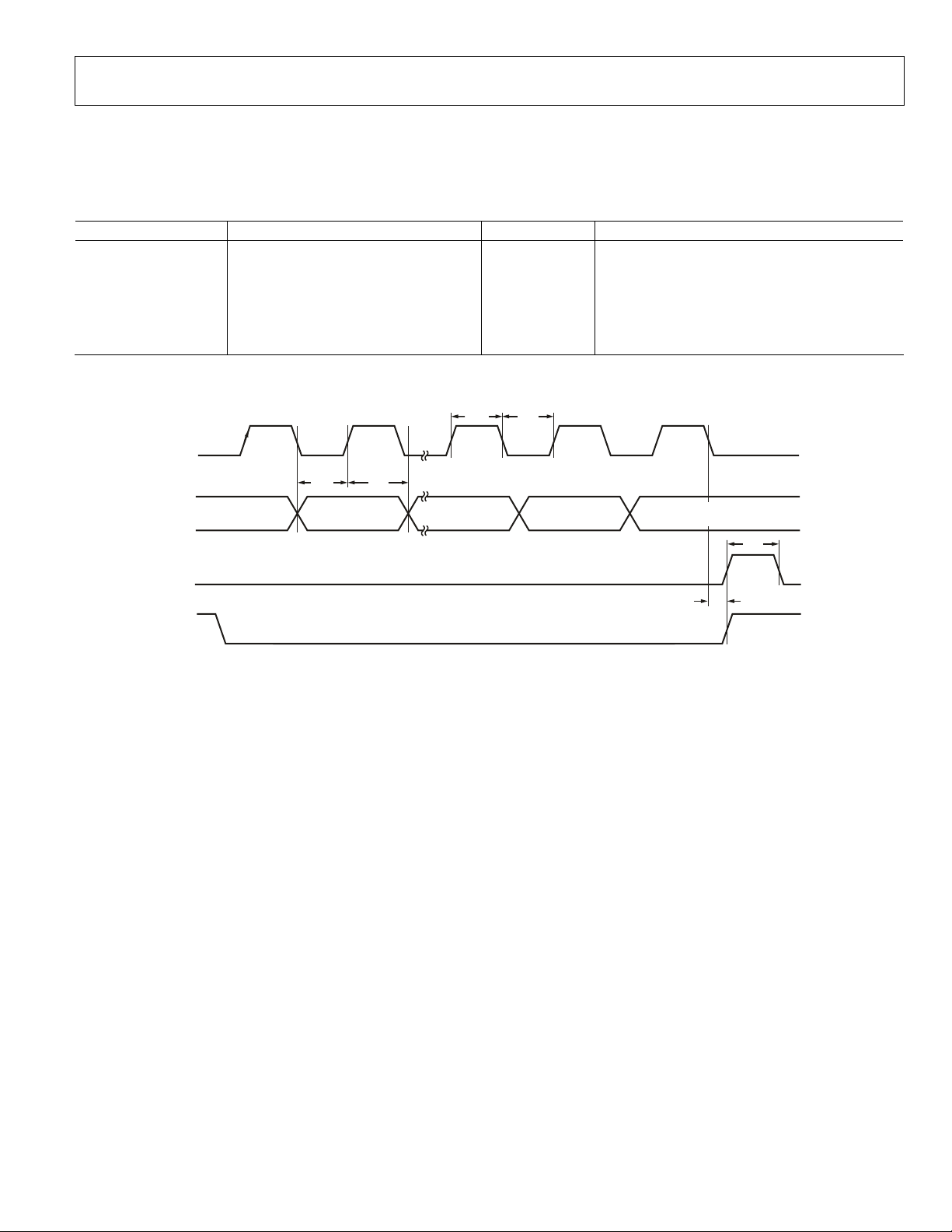
K
TIMING CHARACTERISTICS
Guaranteed by design but not production tested. AVDD = DVDD = 3 V ± 10%, 5 V ± 10%; AVDD ≤ VP ≤ 6 V;
AGND = DGND = CPGND = 0 V; R
= 4.7 kΩ; TA = T
SET
Table 2.
Parameter Limit at T
MIN
to T
(B Version) Unit Test Conditions/Comments
MAX
t1 10 ns min DATA to CLOCK setup time
t2 10 ns min DATA to CLOCK hold time
t3 25 ns min CLOCK high duration
t4 25 ns min CLOCK low duration
t5 10 ns min CLOCK to LE setup time
t6 20 ns min LE pulse width
CLOC
MIN
to T
, unless otherwise noted.
MAX
t
3
t
4
DATA
LE
LE
t
1
DB20 (MSB) DB19 DB2
t
2
DB1
(CONTROL BIT C2)
DB0 (LSB)
(CONTROL BIT C1)
t
5
t
6
03496-0-002
Figure 2. Timing Diagram
Rev. C | Page 5 of 28
Page 6

ADF4110/ADF4111/ADF4112/ADF4113
ABSOLUTE MAXIMUM RATINGS
TA = 25°C, unless otherwise noted
Table 3.
Parameter Rating
AVDD to GND1 −0.3 V to +7 V
AVDD to DVDD −0.3 V to +0.3 V
VP to GND −0.3 V to +7 V
VP to AVDD −0.3 V to +5.5 V
Digital I/O Voltage to GND −0.3 V to VDD + 0.3 V
Analog I/O Voltage to GND −0.3 V to VP + 0.3 V
REFIN, RFINA, RFINB to GND −0.3 V to VDD + 0.3 V
RFINA to RFINB ±320 mV
Operating Temperature Range
Industrial (B Version) −40°C to +85°C
Storage Temperature Range −65°C to +150°C
Maximum Junction Temperature 150°C
TSSOP θJA Thermal Impedance 150.4°C/W
LFCSP θJA Thermal Impedance
(Paddle Soldered)
LFCSP θJA Thermal Impedance
(Paddle Not Soldered)
Lead Temperature, Soldering
Vapor Phase (60 sec) 215°C
Infrared (15 sec) 220°C
122°C/W
216°C/W
1
GND = AGND = DGND = 0 V.
Stresses above those listed under Absolute Maximum Ratings
may cause permanent damage to the device. This is a stress
rating only; functional operation of the device at these or any
other conditions above those listed in the operational sections
of this specification is not implied. Exposure to absolute
maximum rating conditions for extended periods may affect
device reliability.
This device is a high performance RF integrated circuit with an
ESD rating of <2 kV, and it is ESD sensitive. Proper precautions
should be taken for handling and assembly.
TRANSISTOR COUNT
6425 (CMOS) and 303 (Bipolar).
ESD CAUTION
ESD (electrostatic discharge) sensitive device. Electrostatic charges as high as 4000 V readily accumulate on the
human body and test equipment and can discharge without detection. Although this product features
proprietary ESD protection circuitry, permanent damage may occur on devices subjected to high energy
electrostatic discharges. Therefore, proper ESD precautions are recommended to avoid performance
degradation or loss of functionality.
Rev. C | Page 6 of 28
Page 7
ADF4110/ADF4111/ADF4112/ADF4113
C
D
D
PIN CONFIGURATIONS AND FUNCTION DESCRIPTIONS
D
D
P
SET
V
CP
R
SET
CP
PGND
AGND
RF
IN
RF
IN
AV
REF
B
A
DD
IN
1
2
ADF4110
ADF4111
3
ADF4112
4
ADF4113
5
6
TOP VIEW
(Not to Scale)
7
8
16
V
P
15
DV
14
13
12
11
10
9
DD
MUXOUT
LE
DATA
CLK
CE
DGND
03496-0-003
CPGND
AGND
AGND
RF
IN
RF
IN
1
2
3
B
4
5
A
R
19
20
ADF4110
ADF4111
ADF4112
ADF4113
TOP VIEW
(Not to Scale)
6
7
DD
AVDDAV
Figure 3. TSSOP Pin Configuration Figure 4. LFCSP Pin Configuration
Table 4. Pin Function Descriptions
TSSOP
Pin No.
1 19 R
2 20 CP
LFCSP
Pin No.
Mnemonic Function
SET
Connecting a resistor between this pin and CPGND sets the maximum charge pump output current.
The nominal voltage potential at the R
I
=
maxCP
R
So, with R
SET
Charge Pump Output. When enabled, this provides ±I
5.23
SET
= 4.7 kΩ, I
CPmax
= 5 mA.
pin is 0.56 V. The relationship between I
SET
to the external loop filter, which in turn
CP
drives the external VCO.
3 1 CPGND Charge Pump Ground. This is the ground return path for the charge pump.
4 2, 3 AGND Analog Ground. This is the ground return path of the prescaler.
5 4 RFINB
Complementary Input to the RF Prescaler. This point should be decoupled to the ground plane with
a small bypass capacitor, typically 100 pF. See Figure 29.
6 5 RFINA Input to the RF Prescaler. This small-signal input is ac-coupled from the VCO.
7 6, 7 AVDD
Analog Power Supply. This may range from 2.7 V to 5.5 V. Decoupling capacitors to the analog
ground plane should be placed as close as possible to this pin. AV
.
as DV
DD
8 8 REFIN
Reference Input. This is a CMOS input with a nominal threshold of V
resistance of 100 kΩ. See Figure 28. This input can be driven from a TTL or CMOS crystal oscillator,
or can be ac-coupled.
9 9, 10 DGND Digital Ground.
10 11 CE
Chip Enable. A logic low on this pin powers down the device and puts the charge pump output into
three-state mode. Taking the pin high powers up the device depending on the status of the power-
down Bit F2.
11 12 CLK
Serial Clock Input. This serial clock is used to clock in the serial data to the registers. The data is
latched into the 24-bit shift register on the CLK rising edge. This input is a high impedance CMOS
input.
12 13 DATA
Serial Data Input. The serial data is loaded MSB first with the two LSBs being the control bits. This
input is a high impedance CMOS input.
13 14 LE
Load Enable, CMOS Input. When LE goes high, the data stored in the shift registers is loaded into
one of the four latches; the latch is selected using the control bits.
14 15 MUXOUT
This multiplexer output allows either the lock detect, the scaled RF, or the scaled reference
frequency to be accessed externally.
15 16, 17 DVDD
Digital Power Supply. This may range from 2.7 V to 5.5 V. Decoupling capacitors to the digital
ground plane should be placed as close as possible to this pin. DV
.
as AV
DD
16 18 VP
Charge Pump Power Supply. This should be greater than or equal to V
can be set to 6 V and used to drive a VCO with a tuning range of up to 6 V.
3 V, V
P
DV
DV
16
17
18
15
MUXOUT
14
LE
13
DATA
12
CLK
11
CE
9108
IN
REF
DGND
DGND
must be the same value
DD
/2, and an equivalent input
DD
must be the same value
DD
. In systems where VDD is
DD
CP
03496-0-004
and R
is
SET
Rev. C | Page 7 of 28
Page 8
ADF4110/ADF4111/ADF4112/ADF4113
TYPICAL PERFORMANCE CHARACTERISTICS
FREQ PARAM DATA KEYWORD IMPEDANCE
–UNIT –TYPE –FORMAT –OHMS
GHz S MA R 50
FREQ MAGS11 ANGS11
0.05 0.89207 –2.0571
0.10 0.8886 –4.4427
0.15 0.89022 –6.3212
0.20 0.96323 –2.1393
0.25 0.90566 –12.13
0.30 0.90307 –13.52
0.35 0.89318 –15.746
0.40 0.89806 –18.056
0.45 0.89565 –19.693
0.50 0.88538 –22.246
0.55 0.89699 –24.336
0.60 0.89927 –25.948
0.65 0.87797 –28.457
0.70 0.90765 –29.735
0.75 0.88526 –31.879
0.80 0.81267 –32.681
0.85 0.90357 –31.522
0.90 0.92954 –34.222
0.95 0.92087 –36.961
1.00 0.93788 –39.343
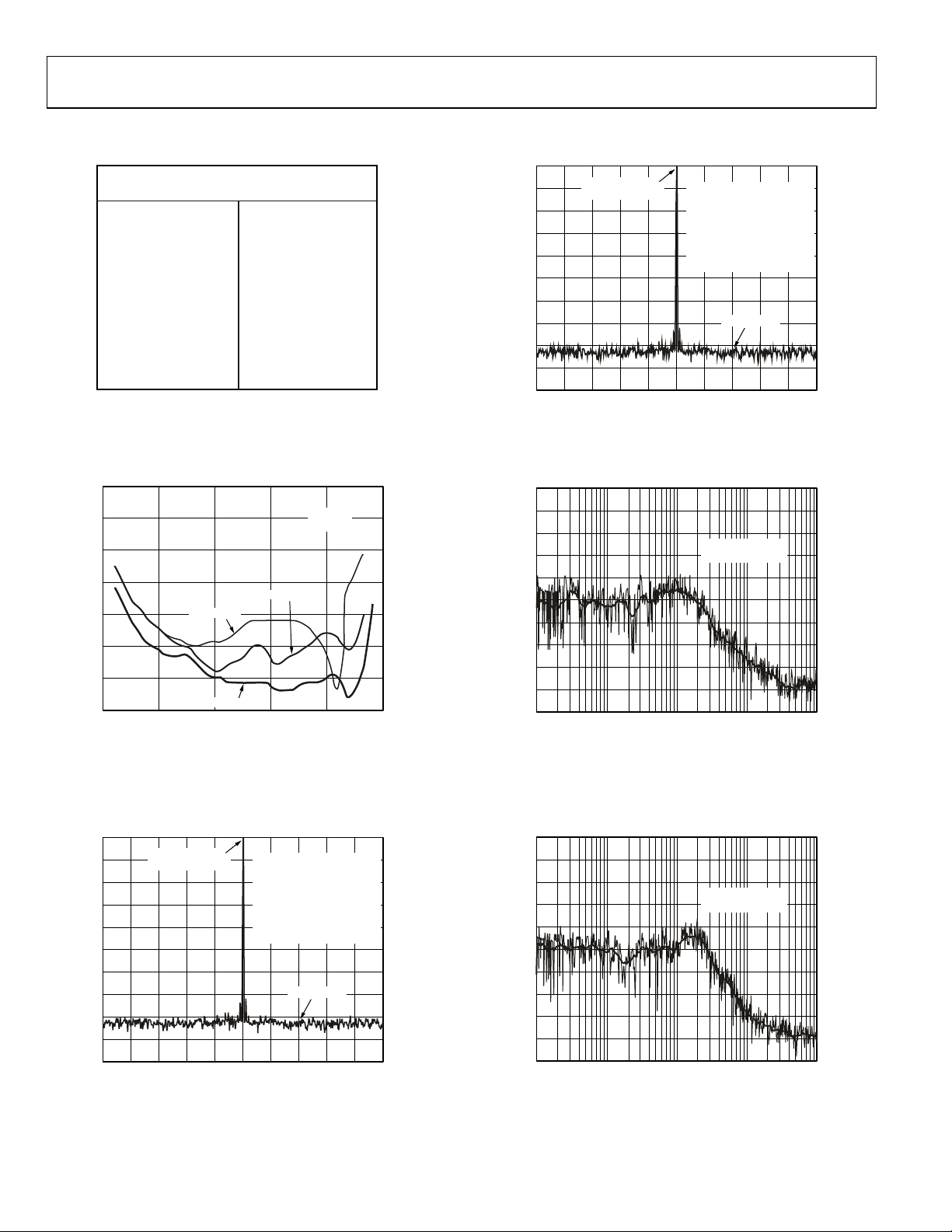
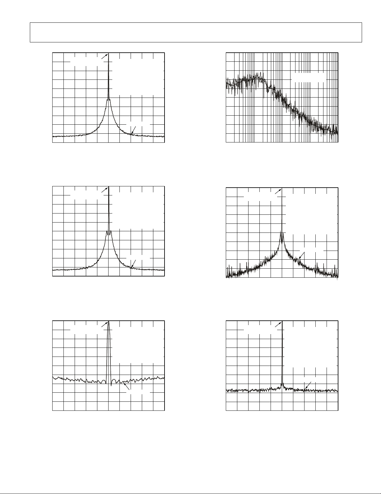
Figure 5. S-Parameter Data for the ADF4113 RF Input (up to 1.8 GHz)
0
–5
–10
–15
–20
–25
RF INPUT POWER (dBm)
–30
–35
012345
T
A
TA = –40°C
RF INPUT FREQUENCY (GHz)
FREQ MAGS11 ANGS11
1.05 0.9512 –40.134
1.10 0.93458 –43.747
1.15 0.94782 –44.393
1.20 0.96875 –46.937
1.25 0.92216 –49.6
1.30 0.93755 –51.884
1.35 0.96178 –51.21
1.40 0.94354 –53.55
1.45 0.95189 –56.786
1.50 0.97647 –58.781
1.55 0.98619 –60.545
1.60 0.95459 –61.43
1.65 0.97945 –61.241
1.70 0.98864 –64.051
1.75 0.97399 –66.19
1.80 0.97216 –63.775
TA = +25°C
= +85°C
VDD = 3V
V
= 3V
P
03496-0-005
03496-0-006
0
–10
–20
–30
–40
–50
–60
–70
OUTPUT POWER (dB)
–80
–90
–100
REFERENCE
LEVEL = –4.2dBm
–2.0kHz –1.0kHz 900MHz 1.0kHz 2.0kHz
VDD = 3V, VP = 5V
I
= 5mA
CP
PFD FREQUENCY = 200kHz
LOOP BANDWIDTH = 20kHz
RES. BANDWIDTH = 10Hz
VIDEO BANDWIDTH = 10Hz
SWEEP = 1.9 s
AVERAGES = 19
FREQUENCY
–92.5dBc/Hz
Figure 8. ADF4113 Phase Noise
(900 MHz, 200kHz, 20 kHz) with DLY and SYNC Enabled
–40
–50
PHASE NOISE (dBc/Hz)
–60
–70
–80
–90
–100
–110
–120
–130
–140
1k100 10k 100k 1M
FREQUENCY OFFSET FROM 900MHz CARRIER (Hz)
RMS NOISE = 0.52°
R
= –40dBc/Hz
L
03496-0-008
03496-0-009
Figure 6. Input Sensitivity (ADF4113)
0
–10
–20
–30
–40
–50
–60
–70
OUTPUT POWER (dB)
–80
–90
–100
REFERENCE
LEVEL = –4.2dBm
–2.0kHz –1.0kHz 900MHz 1.0kHz 2.0kHz
VDD = 3V, VP = 5V
ICP = 5mA
PFD FREQUENCY = 200kHz
LOOP BANDWIDTH = 20kHz
RES. BANDWIDTH = 10Hz
VIDEO BANDWIDTH = 10Hz
SWEEP = 1.9 s
AVERAGES = 19
FREQUENCY
–91.0dBc/Hz
Figure 7 ADF4113 Phase Noise (900 MHz, 200 kHz, 20 kHz)
03496-0-007
Rev. C | Page 8 of 28
Figure 9. ADF4113 Integrated Phase Noise
(900 MHz, 200 kHz, 20 kHz, Typical Lock Time: 400 µs)
–40
–50
PHASE NOISE (dBc/Hz)
–60
–70
–80
–90
–100
–110
–120
–130
–140
1k100 10k 100k 1M
FREQUENCY OFFSET FROM 900MHz CARRIER (Hz)
RMS NOISE = 0.62°
R
L
Figure 10. ADF4113 Integrated Phase Noise
(900 MHz, 200 kHz, 35 kHz, Typical Lock Time: 200 µs)
= –40dBc/Hz
03496-0-010
Page 9
ADF4110/ADF4111/ADF4112/ADF4113
0
–10
–20
–30
–40
–50
–60
–70
OUTPUT POWER (dB)
–80
–90
–100
REFERENCE
LEVEL = –4.2dBm
–400kHz –200kHz 900MHz 200kHz 400kHz
VDD = 3V, VP = 5V
I
= 5mA
CP
PFD FREQUENCY = 200kHz
LOOP BANDWIDTH = 20kHz
RES. BANDWIDTH = 1kHz
VIDEO BANDWIDTH = 1kHz
SWEEP = 2.5s
AVERAGES = 30
FREQUENCY
–90.2dBc/Hz
Figure 11. ADF4113 Reference Spurs (900 MHz, 200 kHz, 20 kHz)
0
–10
–20
–30
–40
–50
–60
–70
OUTPUT POWER (dB)
–80
–90
–100
REFERENCE
LEVEL = –4.2dBm
–400kHz –200kHz 900MHz 200kHz 400kHz
VDD = 3V, VP = 5V
I
= 5mA
CP
PFD FREQUENCY = 200kHz
LOOP BANDWIDTH = 35kHz
RES. BANDWIDTH = 1kHz
VIDEO BANDWIDTH = 1kHz
SWEEP = 2.5s
AVERAGES = 30
FREQUENCY
–89.3dBc/Hz
Figure 12. ADF4113 (900 MHz, 200 kHz, 35 kHz)
0
–10
–20
–30
–40
–50
–60
–70
OUTPUT POWER (dB)
–80
–90
–100
REFERENCE
LEVEL = –8.0dBm
–400Hz –200Hz 1750MHz 200Hz 400Hz
VDD = 3V, VP = 5V
ICP = 5mA
PFD FREQUENCY = 30kHz
LOOP BANDWIDTH = 3kHz
RES. BANDWIDTH = 10kHz
VIDEO BANDWIDTH = 10kHz
SWEEP = 477ms
AVERAGES = 10
FREQUENCY
–75.2dBc/Hz
Figure 13. ADF4113 Phase Noise (1750 MHz, 30 kHz, 3 kHz)
03496-0-011
03496-0-012
03496-0-013
–40
–50
PHASE NOISE (dBc/Hz)
–60
–70
–80
–90
–100
–110
–120
–130
–140
1k100 10k 100k 1M
FREQUENCY OFFSET FROM 1750MHz CARRIER (Hz)
RMS NOISE = 1.6°
RL = –40dBc/Hz
Figure 14. ADF4113 Integrated Phase Noise
(1750 MHz, 30 kHz, 3 kHz)
0
–10
–20
–30
–40
–50
–60
–70
OUTPUT POWER (dB)
–80
–90
–100
REFERENCE
LEVEL = –5.7dBm
–80kHz –40kHz 1750MHz 40kHz 80kHz
VDD = 3V, VP = 5V
I
= 5mA
CP
PFD FREQUENCY = 30kHz
LOOP BANDWIDTH = 3kHz
RES. BANDWIDTH = 3Hz
VIDEO BANDWIDTH = 3Hz
SWEEP = 255s
POSITIVE PEEK DETECT
MODE
FREQUENCY
–79.6dBc/Hz
Figure 15. ADF4113 Reference Spurs (1750 MHz, 30 kHz, 3 kHz)
0
–10
–20
–30
–40
–50
–60
–70
OUTPUT POWER (dB)
–80
–90
–100
REFERENCE
LEVEL = –4.2dBm
–2.0kHz –1.0kHz 3100MHz 1.0kHz 2.0kHz
VDD = 3V, VP = 5V
I
= 5mA
CP
PFD FREQUENCY = 1MHz
LOOP BANDWIDTH = 100kHz
RES. BANDWIDTH = 10Hz
VIDEO BANDWIDTH = 10Hz
SWEEP = 1.9s
AVERAGES = 45
–86.6dBc/Hz
FREQUENCY
Figure 16. ADF4113 Phase Noise (3100 MHz, 1 MHz, 100 kHz)
03496-0-014
03496-0-015
03496-0-016
Rev. C | Page 9 of 28
Page 10

ADF4110/ADF4111/ADF4112/ADF4113
–40
–50
–60
–70
–80
–90
–100
–110
PHASE NOISE (dBc/Hz)
–120
–130
–140
2
10
FREQUENCY OFFSET FROM 3100MHz CARRIER (Hz)
3
10
Figure 17. ADF4113 Integrated Phase Noise
(3100 MHz, 1 MHz, 100 kHz)
0
–10
–20
–30
–40
–50
–60
–70
OUTPUT POWER (dB)
–80
–90
–100
REFERENCE
LEVEL = –17.2dBm
–2.0MHz –1.0MHz 3100MHz 1.0MHz 2.0MHz
FREQUENCY
Figure 18. Reference Spurs (3100 MHz, 1 MHz, 100 kHz)
RMS NOISE = 1.7°
R
= 40dBc/Hz
L
4
10
VDD = 3V, VP = 5V
I
= 5mA
CP
PFD FREQUENCY = 1MHz
LOOP BANDWIDTH = 100kHz
RES. BANDWIDTH = 1kHz
VIDEO BANDWIDTH = 1kHz
SWEEP = 13s
AVERAGES = 1
5
10
–80.6dBc/Hz
6
10
03496-0-017
03496-0-018
–60
VDD = 3V
VP = 3V
–70
–80
PHASE NOISE (dBc/Hz)
–90
–100
–40 –20 0 20 40 60 80 100
TEMPERATURE (°C)
Figure 20. ADF4113 Phase Noise vs. Temperature
(900 MHz, 200 kHz, 20 kHz)
–60
VDD = 3V
V
= 5V
–70
–80
–90
FIRST REFERENCE SPUR (dBc)
–100
–40 –20 0 20 40 60 80 100
TEMPERATURE (°C)
P
Figure 21. ADF4113 Reference Spurs vs. Temperature
(900 MHz, 200 kHz, 20 kHz)
03496-0-020
03496-0-021
–120
–130
–140
–150
–160
PHASE NOISE (dBc/Hz)
–170
–180
101 100 1000 10000
PHASE DETECTOR FREQUENCY (kHz)
Figure 19. ADF4113 Phase Noise (Referred to CP Output)
vs. Phase Detector Frequency
VDD = 3V
V
= 5V
P
03496-0-019
Rev. C | Page 10 of 28
–5
–15
–25
–35
–45
–55
–65
–75
–85
FIRST REFERENCE SPUR (dBc)
–95
–105
012345
TUNING VOLTAGE (V)
Figure 22. ADF4113 Reference Spurs (200 kHz) vs. V
VDD = 3V
V
= 5V
P
TUNE
(900 MHz, 200 kHz, 20 kHz)
03496-0-022
Page 11

ADF4110/ADF4111/ADF4112/ADF4113
–60
–70
VDD = 3V
VP = 5V
3.0
2.5
2.0
VDD = 3V
V
= 3V
P
–80
PHASE NOISE (dBc/Hz)
–90
–100
–40 –20 0 20 40 60 80 100
TEMPERATURE (°C)
Figure 23. ADF4113 Phase Noise vs. Temperature
(836 MHz, 30 kHz, 3 kHz)
–60
VDD = 3V
V
= 5V
–70
–80
–90
FIRST REFERENCE SPUR (dBc)
–100
–40 –20 0 20 40 60 80 100
TEMPERATURE (°C)
P
Figure 24. ADF4113 Reference Spurs vs. Temperature
(836 MHz, 30 kHz, 3 kHz)
10
9
(mA)
DD
AI
8
7
6
5
4
3
2
1
0
ADF4110
ADF4111
ADF4112
8/90 16/17 32/33 64/65
PRESCALER VALUE
Figure 25. AI
ADF4113
vs. Prescaler Value
DD
03496-0-023
03496-0-024
03496-0-025
(mA)
1.5
DD
DI
1.0
0.5
0
500 100 150 200
PRESCALER OUTPUT FREQUENCY (MHz)
Figure 26. DI
vs. Prescaler Output Frequency
DD
03496-0-026
(ADF4110, ADF4111, ADF4112, ADF4113)
6
5
4
3
2
1
0
(mA)
–1
CP
I
–2
–3
–4
–5
–6
0 0.5 1.0 1.5 2.0 2.5 3.0 3.5 4.0 4.5 5.0
V
(V)
CP
VPP = 5V
I
= 5mA
CP
03496-0-027
Figure 27. Charge Pump Output Characteristics for ADF4110 Family
Rev. C | Page 11 of 28
Page 12

ADF4110/ADF4111/ADF4112/ADF4113
CIRCUIT DESCRIPTION
REFERENCE INPUT SECTION
The reference input stage is shown in Figure 28. SW1 and SW2
are normally closed switches. SW3 is normally open. When
power-down is initiated, SW3 is closed and SW1 and SW2 are
opened. This ensures that there is no loading of the REF
on power-down.
POWER-DOWN
CONTROL
100kΩ
NC
SW1
SW2
SW3
NO
REF
IN
NC
Figure 28. Reference Input Stage
BUFFER
TO R COUNTER
RF INPUT STAGE
The RF input stage is shown in Figure 29. It is followed by a
two-stage limiting amplifier to generate the current mode logic
(CML) clock levels needed for the prescaler.
1.6V
AV
DD
500Ω500Ω
RFINA
RF
IN
BIAS
GENERATOR
B
pin
IN
03496-0-028
A AND B COUNTERS
The A and B CMOS counters combine with the dual-modulus
prescaler to allow a wide ranging division ratio in the PLL
feedback counter. The counters are specified to work when the
prescaler output is 200 MHz or less. Thus, with an RF input
frequency of 2.5 GHz, a prescaler value of 16/17 is valid but a
value of 8/9 is not.
Pulse Swallow Function
The A and B counters, in conjunction with the dual-modulus
prescaler, make it possible to generate output frequencies that
are spaced only by the reference frequency divided by R. The
equation for the VCO frequency is
= [(P × B) + A]f
f
VCO
REFIN
/R
where:
f
= output frequency of external voltage controlled oscillator
VCO
(VCO)
P = preset modulus of dual-modulus prescaler
B = preset divide ratio of binary 13-bit counter(3 to 8191)
A = preset divide ratio of binary 6-bit swallow counter (0 to 63)
= output frequency of the external reference frequency
f
REFIN
oscillator
R = preset divide ratio of binary 14-bit programmable reference
counter (1 to 16383)
R COUNTER
The 14-bit R counter allows the input reference frequency to be
divided down to produce the reference clock to the phase
frequency detector (PFD). Division ratios from 1 to 16,383 are
allowed.
AGND
Figure 29. RF Input Stage
03496-0-029
PRESCALER (P/P + 1)
Along with the A and B counters, the dual-modulus prescaler
(P/P + 1) enables the large division ratio, N, to be realized (N =
BP + A). The dual-modulus prescaler, operating at CML levels,
takes the clock from the RF input stage and divides it down to a
manageable frequency for the CMOS A and B counters. The
prescaler is programmable; it can be set in software to 8/9,
16/17, 32/33, or 64/65. It is based on a synchronous 4/5 core.
Rev. C | Page 12 of 28
INPUT STAGE
FROM RF
N = BP + A
PRESCALER
P/P + 1
MODULUS
CONTROL
Figure 30. A and B Counters
13-BIT B
COUNTER
LOAD
LOAD
6-BIT A
COUNTER
TO PFD
03496-0-030
Page 13

ADF4110/ADF4111/ADF4112/ADF4113
A
T
PHASE FREQUENCY DETECTOR (PFD) AND CHARGE PUMP
The PFD takes inputs from the R counter and N counter (N =
BP + A) and produces an output proportional to the phase and
frequency difference between them. Figure 31 is a simplified
schematic. The PFD includes a programmable delay element
that controls the width of the antibacklash pulse. This pulse
ensures that there is no dead zone in the PFD transfer function
and minimizes phase noise and reference spurs. Two bits in the
reference counter latch, ABP2 and ABP1, control the width of
the pulse. See Table 7.
V
P
CHARGE
PUMP
U1
CLR1
UP
Q1D1
HI
R DIVIDER
Lock Detect
MUXOUT can be programmed for two types of lock detect:
digital lock detect and analog lock detect.
Digital lock detect is active high. When LDP in the R counter
latch is set to 0, digital lock detect is set high when the phase
error on three consecutive phase detector (PD) cycles is less
than 15 ns. With LDP set to 1, five consecutive cycles of less
than 15 ns are required to set the lock detect. It stays high until
a phase error greater than 25 ns is detected on any subsequent
PD cycle.
The N-channel open-drain analog lock detect should be
operated with a 10 kΩ nominal external pull-up resistor. When
lock has been detected, this output is high with narrow lowgoing pulses.
DV
DD
HI
N DIVIDER
R DIVIDER
N DIVIDER
CP OUTPUT
PROGRAMMABLE
ABP1 ABP2
CLR2
Q2D2
U2
DELAY
DOWN
U3
CPGND
CP
Figure 31. PFD Simplified Schematic and Timing (In Lock)
MUXOUT AND LOCK DETECT
The output multiplexer on the ADF4110 family allows the user
to access various internal points on the chip. The state of
MUXOUT is controlled by M3, M2, and M1 in the function
latch. Table 9 shows the full truth table. Figure 32 shows the
MUXOUT section in block diagram form.
NALOG LOCK DETEC
DIGITAL LOCK DETECT
R COUNTER OUTPUT
N COUNTER OUTPUT
SDOUT
CONTROLMUX
DGND
MUXOUT
03496-0-032
Figure 32. MUXOUT Circuit
INPUT SHIFT REGISTER
The ADF4110 family digital section includes a 24-bit input shift
register, a 14-bit R counter, and a 19-bit N counter comprised of
a 6-bit A counter and a 13-bit B counter. Data is clocked into the
03496-0-031
24-bit shift register on each rising edge of CLK MSB first. Data
is transferred from the shift register to one of four latches on
the rising edge of LE. The destination latch is determined by the
state of the two control bits (C2, C1) in the shift register. These
are the two LSBs, DB1 and DB0, as shown in Figure 2. The truth
table for these bits is shown in Table 5.
Table 6 shows a summary of how the latches are programmed.
Table 5. C2, C1 Truth Table
Control Bits
C2 C1 Data Latch
0 0 R Counter
0 1 N Counter (A and B)
1 0 Function Latch (Including Prescaler)
1 1 Initialization Latch
Rev. C | Page 13 of 28
Page 14

ADF4110/ADF4111/ADF4112/ADF4113
Table 6. ADF4110 Family Latch Summary
REFERENCE COUNTER LATCH
DEVRESER
SYNC
DLY
KCOL
NOISICERP
TCETED
TEST
MODE BITS
ANTI-
BACKLASH
WIDTH
14-BIT REFERENCE COUNTER, R
CONTROL
BITS
DB22
DB23
X
X = DON'T CARE
RESERVED
DB23
DB22
XX
X = DON'T CARE
PRESCALER
VALUE
DB22
DB23
P1P2
DB21
DB20
DB19
LDP T2 T1 R14 R13 R12 R11 R10 R8 R7 R6 R5 R4 R3 R2 R1 C2 (0) C1 (0)R9
SYNCDLY ABP2 ABP1
DB18
DB17
DB16
DB15
DB14
DB13
N COUNTER LATCH
NIAGPC
13-BIT B COUNTER
DB21
G1 B10 B9
DB19
DB20
B13 B12 B11 B8 B7 B6 B5 B4 B2 B1 A6 A5 A4 A3 A2 A1 C2 (0) C1 (1)B3
DB18
DB17
DB16
DB15
DB14
DB13
FUNCTION LATCH
-REWOP
2NWOD
CURRENT
SETTING
2
DB21
DB20
PD2 CPI3 CPI2
CPI6 CPI5 CPI4 CPI1 TC4 TC3 TC2 TC1 F4 F3 F2 M3 M2 M1 PD1 F1 C2 (1) C1 (0)F5
DB19
DB18
DB17
CURRENT
SETTING
1
DB16
DB15
TIMER COUNTER
CONTROL
DB13
DB14
DB12 DB11
DB12 DB11 DB10
DB12
DB10 DB9 DB8
DB11 DB10 DB9
DB9 DB8 DB7
KCOLTSAF
KCOLTSAF
ELBANE
EDOM
DB7
-EERHT
ETATS
P
DP
C
DB8 DB7
DB6 DB5 DB4
6-BIT A COUNTER
DB5
DB6
YTIRALOP
MUXOUT
CONTROL
DB6
DB5 DB4
DB4
DB3
DB3
DB3
-REWOP
1NWOD
DB2
DB1
CONTROL
DB2 DB1
RETNUOC
TESER
CONTROL
DB2 DB1
DB0
BITS
DB0
BITS
DB0
PRESCALER
DB23
VALUE
-REWOP
2NWOD
CURRENT
SETTING
2
DB21
DB22
PD2 CPI3 CPI2
P1P2
DB19
DB20
CPI6 CPI5 CPI4 CPI1 TC4 TC3 TC2 TC1 F4 F3 F2 M3 M2 M1 PD1 F1 C2 (1) C1 (1)F5
DB18
DB17
CURRENT
SETTING
1
DB16
DB15
INITIALIZATION LATCH
TIMER COUNTER
CONTROL
DB14
DB12 DB11 DB10 DB9
DB13
Rev. C | Page 14 of 28
KCOLTSAF
ELBANE
ETATS-EERHT
PC
DB8 DB7
YTIRALOP
DP
DB6
MUXOUT
CONTROL
DB5
DB4
-REWOP
DB3
RETNUOC
1NWOD
DB2 DB1
TESER
CONTROL
BITS
DB0
03496-0-033
KCOLTSAF
EDOM
Page 15

ADF4110/ADF4111/ADF4112/ADF4113
Table 7. Reference Counter Latch Map
DEVRESER
DLY
SYNC
KCOL
NOISICERP
TCETED
TEST
MODE BITS
ANTI-
BACKLASH
WIDTH
14-BIT REFERENCE COUNTER
CONTROL
BITS
DB23
X
X = DON'T
DB22
CARE
DB20
DB21
SYNCDLY ABP2 ABP1
LDP T2 T1 R14 R13 R12 R11 R10 R8 R7 R6 R5 R4 R3 R2 R1 C2 (0) C1 (0)R9
DB19
DB18
DB17
0
0
1
1
DB16
ABP1ABP2
0
1
0
1
DB14
DB15
ANTIBACKLASH PULSE WIDTH
3.0ns
1.5ns
6.0ns
3.0ns
DB12 DB11 DB10
DB13
R14
0
0
0
0
•
•
•
1
1
1
1
DB9 DB8 DB7
R13
0
0
0
0
•
•
•
1
1
1
1
R12
0
0
0
0
•
•
•
1
1
1
1
••••••••••
••••••••• •
••••••••• •
••••••••• •
••••••••• •
••••••••• •
••••••••• •
••••••••• •
••••••••• •
••••••••• •
••••••••• •
••••••••• •
DB6
DB5
DB4 DB3
R3
R2
0
0
0
1
0
1
1
0
•
•
•
•
•
•
1
0
1
0
1
1
1
1
R1
1
0
1
0
•
•
•
0
1
0
1
DB2 DB1
DIVIDE RATIO
DB0
1
2
3
4
•
•
•
16380
16381
16382
16383
TEST MODE BITS SHOULD
BE SET TO 00 FOR NORMAL
OPERATION
OPERATION
LDP
THREE CONSECUTIVE CYCLES OF PHASE DELAY LESS THAN
0
15ns MUST OCCUR BEFORE LOCK DETECT IS SET.
FIVE CONSECUTIVE CYCLES OF PHASE DELAY LESS THAN
1
15ns MUST OCCUR BEFORE LOCK DETECT IS SET.
OPERATION
SYNCDLY
0
0
NORMAL OPERATION
0
1
OUTPUT OF PRESCALER IS RESYNCHRONIZED
WITH NONDELAYED VERSION OF RF INPUT
1
0
NORMAL OPERATION
1
1
OUTPUT OF PRESCALER IS RESYNCHRONIZED
WITH DELAYED VERSION OF RF INPUT
03496-0-034
Rev. C | Page 15 of 28
Page 16
ADF4110/ADF4111/ADF4112/ADF4113
Table 8. AB Counter Latch Map
NIAGPC
RESERVED
13-BIT B COUNTER
6-BIT A COUNTER
CONTROL
BITS
DB23
X
DB21
DB22
X
DB20
DB19
B13 B12 B11 B8 B7 B6 B5 B4 B2 B1 A6 A5 A4 A3 A2 A1B3
G1 B10 B9
X = DON'T CARE
B13
0
0
0
0
0
•
•
•
1
1
1
1
DB18
DB17
B12
0
0
0
0
0
•
•
•
1
1
1
1
DB16
B11
0
0
0
0
0
•
•
•
1
1
1
1
DB15
DB14
••••••••• •
••••••••• •
••••••••• •
••••••••• •
••••••••• •
••••••••• •
••••••••• •
••••••••• •
••••••••• •
••••••••• •
••••••••• •
••••••••• •
••••••••• •
DB12
DB13
DB11 DB10 DB9
A6
0
0
0
0
•
•
•
1
1
1
1
B3 B2 B1 B COUNTER DIVIDE RATIO
0
0
0
0
1
•
•
•
1
1
1
1
0
0
1
1
0
•
•
•
0
0
1
1
0
1
0
1
0
•
•
•
0
1
0
1
DB8 DB7
A5
0
0
0
0
•
•
•
1
1
1
1
••••••••• •
••••••••• •
••••••••• •
••••••••• •
••••••••• •
••••••••• •
••••••••• •
••••••••• •
••••••••• •
••••••••• •
••••••••• •
••••••••• •
NOT ALLOWED
NOT ALLOWED
NOT ALLOWED
3
4
8188
8189
8190
8191
•
•
•
DB6
DB5 DB4
A2
0
0
1
1
•
•
•
0
0
1
1
DB3
A1
0
1
0
1
•
•
•
0
1
0
1
DB1
DB2
C2 (0) C1 (1)
A COUNTER
DIVIDE RATIO
0
1
2
3
•
•
•
60
61
62
63
DB0
F4 (FUNCTION LATCH)
FASTLOCK ENABLE*
0
0
1
1
*SEE TABLE 9
THESE BITS ARE NOT USED
BY THE DEVICE AND ARE
DON'T CARE BITS
CP GAIN OPERATION
0
1
0
1
CHARGE PUMP CURRENT SETTING 1
IS PERMANENTLY USED.
CHARGE PUMP CURRENT SETTING 2
IS PERMANENTLY USED.
CHARGE PUMP CURRENT SETTING 1
IS USED.
CHARGE PUMP CURRENT IS SWITCHED
TO SETTING 2. THE TIME SPENT IN
SETTING 2 IS DEPENDENT UPON WHICH
FASTLOCK MODE IS USED. SEE FUNCTION
LATCH DESCRIPTION.
Rev. C | Page 16 of 28
N = BP + A, P IS PRESCALER VALUE SET IN THE
FUNCTION LATCH, B MUST BE GREATER THAN OR
EQUAL TO A. FOR CONTINUOUSLY ADJACENT VALUES
OF (N
), AT THE OUTPUT, N
XFREF
MIN
IS (P2–P).
03496-0-035
Page 17

ADF4110/ADF4111/ADF4112/ADF4113
Table 9. Function Latch Map
ETATS-EERHT
KCOLTSAF
ELBANE
PC
DB8 DB7
F3
CHARGE PUMP OUTPUT
0
1
F5
FASTLOCK MODE
FASTLOCK DISABLED
X
FASTLOCK MODE 1
0
FASTLOCK MODE 2
1
TIMEOUT
(PFD CYCLES)
3
7
11
15
19
23
27
31
35
39
43
47
51
55
59
63
YTIRALOP
DP
DB6
PHASE DETECTOR
F2
POLARITY
0
NEGATIVE
1
POSITIVE
NORMAL
THREE-STATE
MUXOUT
CONTROL
DB5 DB4
M3
0
0
0
0
1
1
1
1
RETNUOC
-REWOP
1NWOD
TESER
CONTROL
BITS
DB2 DB1
DB3
F1
NORMAL
0
R, A, B COUNTERS
1
HELD IN RESET
M2
M1
0
0
1
1
0
0
1
1
THREE-STATE OUTPUT
0
DIGITAL LOCK DETECT
1
(ACTIVE HIGH)
N DIVIDER OUTPUT
0
DV
1
0
R DIVIDER OUTPUT
1
ANALOG LOCK DETECT
(N-CHANNEL OPEN-DRAIN)
0
SERIAL DATA OUTPUT
1
DGND
COUNTER
OPERATION
OUTPUT
DD
DB0
PRESCALER
VALUE
DB22
DB23
P2
-REWOP
2NWOD
CURRENT
SETTING
2
DB21
DB20
DB19
CPI6 CPI5 CPI4 CPI1 TC4 TC3 TC2 TC1 F4 F3 F2 M3 M2 M1 PD1 F1 C2(1) C1(0)F5
PD2P1 CPI3 CPI2
CPI6
CPI3
0
0
0
0
1
1
1
1
DB18
CPI5
CPI2
CURRENT
SETTING
1
DB17
DB16
TC4
0
0
0
0
0
0
0
0
1
1
1
1
1
1
1
1
CPI4
2.7kΩ 4.7kΩ 10kΩ
CPI1
0
0
1
0
0
1
1
1
0
0
1
0
0
1
1
1
DB15
1.09
2.18
3.26
4.35
5.44
6.53
7.62
8.70
TIMER COUNTER
DB14
DB13
TC3
0
0
0
0
1
1
1
1
0
0
0
0
1
1
1
1
ICP (mA)
0.63
1.25
1.88
2.50
3.13
3.75
4.38
5.00
CONTROL
0.29
0.59
0.88
1.76
1.47
1.76
2.06
2.35
KCOLTSAF
EDOM
DB12 DB11 DB10 DB9
F4
0
1
1
TC2
TC1
0
0
0
1
1
0
1
1
0
0
0
1
1
0
1
1
0
0
0
1
1
0
1
1
0
0
0
1
1
0
1
1
SEE FUNCTION LATCH,
TIMER COUNTER CONTROL
SECTION
CE PIN
PD2 PD1 MODE
0
1
1
1
P2
P1
PRESCALER VALUE
0
0
1
1
8/9
0
16/17
1
32/33
0
64/65
1
ASYNCHRONOUS POWER-DOWN
X
X
NORMAL OPERATION
X
0
ASYNCHRONOUS POWER-DOWN
0
1
1
1
SYNCHRONOUS POWER-DOWN
03496-0-036
Rev. C | Page 17 of 28
Page 18

ADF4110/ADF4111/ADF4112/ADF4113
Table 10. Initialization Latch Map
-REWOP
2NWOD
CPI5
CPI2
CURRENT
SETTING
1
DB16
DB17
0
0
1
1
0
0
1
1
DB15
TC4
0
0
0
0
0
0
0
0
1
1
1
1
1
1
1
1
CPI4
2.7kΩ 4.7kΩ 10kΩ
CPI1
0
1
0
1
0
1
0
1
1.09
2.18
3.27
4.35
5.44
6.53
7.62
8.70
TIMER COUNTER
DB14
TC4
TC3
0
0
0
0
1
1
1
1
0
0
0
0
1
1
1
1
I
(mA)
CP
0.63
1.25
1.88
2.50
3.13
3.75
4.38
5.00
CONTROL
DB13
TC3 TC2 TC1
PRESCALER
VALUE
DB22
DB23
P2
CURRENT
SETTING
2
DB20
DB21
CPI6 CPI5 CPI4 CPI1
PD2P1 CPI3 CPI2
CPI6
CPI3
DB19
0
0
0
0
1
1
1
1
DB18
DB12 DB11
TC2
0
0
1
1
0
0
1
1
0
0
1
1
0
0
1
1
0.29
0.59
0.88
1.76
1.47
1.76
2.06
2.35
ETATS-EERHT
KCOLTSAF
KCOLTSAF
ELBANE
EDOM
DB10
DB9 DB8 DB7
F4 F3 F2 M3 M2 M1 PD1 F1
F5
F3
0
1
F4
0
1
1
TC1
SEE FUNCTION LATCH,
TIMER COUNTER CONTROL
SECTION
F5
X
0
1
0
1
0
1
0
1
0
1
0
1
0
1
0
1
0
1
FASTLOCK MODE
FASTLOCK DISABLED
FASTLOCK MODE 1
FASTLOCK MODE 2
(PFD CYCLES)
YTIRALOP
PC
DP
PHASE DETECTOR
F2
0
1
CHARGE PUMP
OUTPUT NORMAL
THREE-STATE
TIMEOUT
3
7
11
15
19
23
27
31
35
39
43
47
51
55
59
63
MUXOUT
CONTROL
DB6
POLARITY
NEGATIVE
POSITIVE
DB5
M3
0
0
0
0
1
1
1
1
DB4
M2
0
0
1
1
0
0
1
1
RETNUOC
-REWOP
1NWOD
TESER
DB3
DB2
COUNTER
F1
OPERATION
0
NORMAL
1
R, A, B COUNTERS
HELD IN RESET
M1
THREE-STATE OUTPUT
0
DIGITAL LOCK DETECT
1
(ACTIVE HIGH)
N DIVIDER OUTPUT
0
DV
1
0
1
0
1
DD
R DIVIDER OUTPUT
ANALOG LOCK DETECT
(N-CHANNEL OPEN-DRAIN)
SERIAL DATA OUTPUT
DGND
CONTROL
BITS
DB1
DB0
C2 (1) C1 (1)
OUTPUT
P2
0
0
1
1
CE PIN PD2 PD1
0
1
1
1
PRESCALER VALUE
P1
8/9
0
16/17
1
32/33
0
64/65
1
MODE
X
X
0
1
ASYNCHRONOUS POWER-DOWN
X
NORMAL OPERATION
0
ASYNCHRONOUS POWER-DOWN
1
1
SYNCHRONOUS POWER-DOWN
03496-0-037
Rev. C | Page 18 of 28
Page 19

ADF4110/ADF4111/ADF4112/ADF4113
FUNCTION LATCH
The on-chip function latch is programmed with C2, C1 set to 1.
Table 9 shows the input data format for programming the
function latch.
Counter Reset
DB2 (F1) is the counter reset bit. When DB2 is 1, the R counter
and the AB counters are reset. For normal operation, this bit
should be 0. Upon powering up, the F1 bit must be disabled, and
the N counter resumes counting in “close” alignment with the R
counter. (The maximum error is one prescaler cycle.)
Power-Down
DB3 (PD1) and DB21 (PD2) on the ADF411x provide programmable power-down modes. They are enabled by the CE pin.
Fastlock Mode Bit
DB10 of the function latch is the fastlock enable bit. When
fastlock is enabled, this bit determines which fastlock mode is
used. If the fastlock mode bit is 0, fastlock mode 1 is selected; if
the fastlock mode bit is 1, fastlock mode 2 is selected.
Fastlock Mode 1
The charge pump current is switched to the contents of Current
Setting 2.
The device enters fastlock by having a 1 written to the CP gain
bit in the AB counter latch. The device exits fastlock by having a
0 written to the CP gain bit in the AB counter latch.
When the CE pin is low, the device is immediately disabled
regardless of the states of PD2, PD1.
In the programmed asynchronous power-down, the device
powers down immediately after latching a 1 into Bit PD1,
provided PD2 has been loaded with a 0.
In the programmed synchronous power-down, the device
power-down is gated by the charge pump to prevent unwanted
frequency jumps. Once power-down is enabled by writing a 1
into Bit PD1 (provided a 1 has also been loaded to PD2), the
device goes into power-down on the next charge pump event.
When a power-down is activated (either synchronous or
asynchronous mode including CE pin activated power-down),
the following events occur:
• All active dc current paths are removed.
• The R, N, and timeout counters are forced to their load
state conditions.
• The charge pump is forced into three-state mode.
• The digital clock detect circuitry is reset.
• The RFIN input is debiased.
• The reference input buffer circuitry is disabled.
• The input register remains active and capable of loading
and latching data.
MUXOUT Control
The on-chip multiplexer is controlled by M3, M2, and M1 on
the ADF4110 family. Table 9 shows the truth table.
Fastlock Enable Bit
DB9 of the function latch is the fastlock enable bit. Fastlock is
enables only when this is 1.
Fastlock Mode 2
The charge pump current is switched to the contents of Current
Setting 2. The device enters fastlock by having a 1 written to the
CP gain bit in the AB counter latch. The device exits fastlock
under the control of the timer counter. After the timeout period
determined by the value in TC4 through TC1, the CP gain bit in
the AB counter latch is automatically reset to 0 and the device
reverts to normal mode instead of fastlock. See Table 9 for the
timeout periods.
Timer Counter Control
The user has the option of programming two charge pump currents. Current Setting 1 is meant to be used when the RF output
is stable and the system is in a static state. Current Setting 2 is
meant to be used when the system is dynamic and in a state of
change (i.e., when a new output frequency is programmed).
The normal sequence of events is as follows:
The user initially decides what the preferred charge pump
currents are going to be. For example, they may choose 2.5 mA
as Current Setting 1 and 5 mA as Current Setting 2.
At the same time, they must also decide how long they want the
secondary current to stay active before reverting to the primary
current. This is controlled by the timer counter control bits,
DB14 through DB11 (TC4 through TC1) in the function latch.
The truth table is given in Table 10.
A user can program a new output frequency simply by programming the AB counter latch with new values for A and B. At
the same time, the CP gain bit can be set to 1, which sets the
charge pump with the value in CPI6–CPI4 for a period determined by TC4 through TC1. When this time is up, the charge
pump current reverts to the value set by CPI3–CPI1. At the
same time, the CP gain bit in the AB counter latch is reset to 0
and is ready for the next time the user wishes to change the
frequency.
Rev. C | Page 19 of 28
Page 20

ADF4110/ADF4111/ADF4112/ADF4113
Note that there is an enable feature on the timer counter. It is
enabled when Fastlock Mode 2 is chosen by setting the fastlock
mode bit (DB10) in the function latch to 1.
Charge Pump Currents
CPI3, CPI2, and CPI1 program Current Setting 1 for the charge
pump. CPI6, CPI5, and CPI4 program Current Setting 2 for the
charge pump. The truth table is given in Table 10.
Prescaler Value
P2 and P1 in the function latch set the prescaler values. The
prescaler value should be chosen so that the prescaler output
frequency is always less than or equal to 200 MHz. Thus, with
an RF frequency of 2 GHz, a prescaler value of 16/17 is valid but
a value of 8/9 is not.
PD Polarity
This bit sets the phase detector polarity bit. See Table 10.
CP Three-State
This bit controls the CP output pin. With the bit set high, the CP
output is put into three-state. With the bit set low, the CP output
is enabled.
INITIALIZATION LATCH
When C2, C1 = 1, 1, the initialization latch is programmed. This
is essentially the same as the function latch (programmed when
C2, C1 = 1, 0).
However, when the initialization latch is programmed, an additional internal reset pulse is applied to the R and AB counters.
This pulse ensures that the AB counter is at load point when the
AB counter data is latched, and the device begins counting in
close phase alignment.
If the latch is programmed for synchronous power-down (CE
pin high; PD1 bit high; PD2 bit low), the internal pulse also
triggers this power-down. The prescaler reference and the
oscillator input buffer are unaffected by the internal reset pulse,
so close phase alignment is maintained when counting resumes.
When the first AB counter data is latched after initialization, the
internal reset pulse is again activated. However, successive AB
counter loads after this will not trigger the internal reset pulse.
DEVICE PROGRAMMING AFTER INITIAL POWER-UP
After initial power-up of the device, there are three ways to
program the device.
Initialization Latch Method
Apply V
input word). Make sure the F1 bit is programmed to 0. Then, do
an R load (00 in 2 LSBs). Then do an AB load (01 in 2 LSBs).
. Program the initialization latch (11 in 2 LSBs of
DD
When the initialization latch is loaded, the following occurs:
1. The function latch contents are loaded.
2. An internal pulse resets the R, A, B, and timeout counters
to load state conditions and three-states the charge pump.
Note that the prescaler band gap reference and the oscillator input buffer are unaffected by the internal reset pulse,
allowing close phase alignment when counting resumes.
3. Latching the first AB counter data after the initialization
word activates the same internal reset pulse. Successive AB
loads do not trigger the internal reset pulse unless there is
another initialization.
CE Pin Method
1. Apply V
DD
.
2. Bring CE low to put the device into power-down. This is an
asynchronous power-down in that it happens immediately.
3. Program the function latch (10). Program the R counter
latch (00). Program the AB counter latch (01).
4. Bring CE high to take the device out of power-down. The R
and AB counters now resume counting in close alignment.
After CE goes high, a duration of 1 µs may be required for the
prescaler band gap voltage and oscillator input buffer bias to
reach steady state.
CE can be used to power the device up and down in order to
check for channel activity. The input register does not need to
be reprogrammed each time the device is disabled and enabled
as long as it has been programmed at least once after V
DD
was
initially applied.
Counter Reset Method
1. Apply V
DD
.
2. Do a function latch load (10 in 2 LSBs). As part of this, load
1 to the F1 bit. This enables the counter reset.
3. Do an R counter load (00 in 2 LSBs). Do an AB counter
load (01 in 2 LSBs). Do a function latch load (10 in 2 LSBs).
As part of this, load 0 to the F1 bit. This disables the
counter reset.
This sequence provides the same close alignment as the initialization method. It offers direct control over the internal reset.
Note that counter reset holds the counters at load point and
three states the charge pump but does not trigger synchronous
power-down. The counter reset method requires an extra
function latch load compared to the initialization latch method.
Rev. C | Page 20 of 28
Page 21

ADF4110/ADF4111/ADF4112/ADF4113
RESYNCHRONIZING THE PRESCALER OUTPUT
Table 7 (the Reference Counter Latch Map) shows two bits,
DB22 and DB21, which are labeled DLY and SYNC, respectively.
These bits affect the operation of the prescaler.
With SYNC = 1, the prescaler output is resynchronized with the
RF input. This has the effect of reducing jitter due to the
prescaler and can lead to an overall improvement in synthesizer
phase noise performance. Typically, a 1 dB to 2 dB improvement
is seen in the ADF4113. The lower bandwidth devices can show
an even greater improvement. For example, the ADF4110 phase
noise is typically improved by 3 dB when SYNC is enabled.
With DLY = 1, the prescaler output is resynchronized with a
delayed version of the RF input.
If the SYNC feature is used on the synthesizer, some care must
be taken. At some point, (at certain temperatures and output
frequencies), the delay through the prescaler coincides with the
active edge on RF input; this causes the SYNC feature to break
down. It is important to be aware of this when using the SYNC
feature. Adding a delay to the RF signal, by programming
DLY = 1, extends the operating frequency and temperature
somewhat. Using the SYNC feature also increases the value of
the AI
AI
for the device. With a 900 MHz output, the ADF4113
DD
increases by about 1.3 mA when SYNC is enabled and by
DD
an additional 0.3 mA if DLY is enabled.
All the typical performance plots in this data sheet, except for
Figure 8, apply for DLY and SYNC = 0, i.e., no resynchronization or delay enabled.
Rev. C | Page 21 of 28
Page 22

ADF4110/ADF4111/ADF4112/ADF4113
APPLICATIONS
LOCAL OSCILLATOR FOR GSM BASE STATION TRANSMITTER
Figure 33 shows the ADF4111/ADF4112/ADF4113 being used
with a VCO to produce the LO for a GSM base station
transmitter.
The reference input signal is applied to the circuit at FREF
IN
and, in this case, is terminated in 50 Ω. A typical GSM system
would have a 13 MHz TCXO driving the reference input without any 50 Ω termination. In order to have channel spacing of
200 kHz (GSM standard), the reference input must be divided
by 65, using the on-chip reference divider of the ADF4111/
ADF4112/ADF4113.
The charge pump output of the ADF4111/ADF4112/ADF4113
(Pin 2) drives the loop filter. In calculating the loop filter
component values, a number of items need to be considered. In
this example, the loop filter was designed so that the overall
phase margin for the system would be 45 degrees. Other PLL
system specifications are
= 5 mA
K
D
K
= 12 MHz/V
V
Loop Bandwidth = 20 kHz
= 200 kHz
F
REF
N = 4500
Extra Reference Spur Attenuation = 10 dB
All of these specifications are needed and used to come up with
the loop filter component values shown in Figure 33.
The loop filter output drives the VCO, which in turn is fed back
to the RF input of the PLL synthesizer. It also drives the RF output terminal. A T-circuit configuration provides 50 Ω matching
between the VCO output, the RF output, and the RF
of the synthesizer.
In a PLL system, it is important to know when the system is in
lock. In Figure 33, this is accomplished by using the MUXOUT
signal from the synthesizer. The MUXOUT pin can be programmed to monitor various internal signals in the synthesizer.
One of these is the LD or lock-detect signal.
terminal
IN
FREF
IN
1000pF
SPI COMPATIBLE SERIAL BUS
51Ω
1
1000pF
4.7kΩ
8
1
V
AV
REF
CE
CLK
DATA
LE
R
CPGND
DD
7
DDDVDD
V
P
16
15
V
P
2
CP
IN
1nF
3.3kΩ
5.6kΩ
ADF4111
ADF4112
ADF4113
MUXOUT
RFINA
SET
RF
AGND
43
9
IN
DGND
LOCK
14
DETECT
100pF
6
B
5
100pF
8.2nF
2
51Ω
1
TO BE USED WHEN GENERATOR SOURCE IMPEDANCE IS 50Ω.
2
OPTIONAL MATCHING RESISTOR DEPENDING ON RF
DECOUPLING CAPACITORS ON AV
AND ON THE POSITIVE SUPPLY OF THE VCO190-902T HAVE BEEN
OMITTED FROM THE DIAGRAM TO INCREASE CLARITY.
Figure 33. Local Oscillator for GSM Base Station
620pF
B
V
CC
C
VCO190-902T
DD
100pF
100pF
P
, DVDD, AND VP OF THE ADF411x
18Ω
FREQUENCY.
OUT
RF
18Ω
18Ω
OUT
03496-0-038
Rev. C | Page 22 of 28
Page 23

ADF4110/ADF4111/ADF4112/ADF4113
RF
OUT
100pF
2
FREF
REF
IN
8
CP
IN
ADF4111
ADF4112
ADF4113
CE
CLK
DATA
MUXOUT
LE
1
R
SET
AD5320
12-BIT
RFINA
RF
IN
2.7kΩ
V-OUT DAC
SPI COMPATIBLE SERIAL BUS
LOCK
14
DETECT
100pF
6
5
B
100pF
POWER SUPPLY CONNECTIONS AND DECOUPLING
CAPACITORS ARE OMITTED FOR CLARITY.
Figure 34. Driving the R
USING A D/A CONVERTER TO DRIVE THE R
A D/A converter can be used to drive the R
pin of the
SET
SET
PIN
ADF4110 family, thus increasing the level of control over the
charge pump current, I
. This can be advantageous in wide-
CP
band applications where the sensitivity of the VCO varies over
the tuning range. To compensate for this, the I
may be varied
CP
to maintain good phase margin and ensure loop stability. See
Figure 34.
SHUTDOWN CIRCUIT
The attached circuit in Figure 35 shows how to shut down both
the ADF4110 family and the accompanying VCO. The ADG701
switch goes closed circuit when a Logic 1 is applied to the IN
input. The low cost switch is available in both SOT-23 and
MSOP packages.
WIDEBAND PLL
Many of the wireless applications for synthesizers and VCOs in
PLLs are narrow band in nature. These applications include the
various wireless standards like GSM, DSC1800, CDMA, and
WCDMA. In each of these cases, the total tuning range for the
local oscillator is less than 100 MHz. However, there are also
wideband applications for which the local oscillator could have
LOOP
FILTER
51Ω
Pin with a D/A Converter
SET
a tuning range as wide as an octave. For example, cable TV
tuners have a total range of about 400 MHz. Figure 36 shows an
application where the ADF4113 is used to control and program
the Micronetics M3500-2235. The loop filter was designed for
an RF output of 2900 MHz, a loop bandwidth of 40 kHz, a PFD
frequency of 1 MHz, I
multiplied by the gain factor of 4), VCO K
(sensitivity of the M3500-2235 at an output of 2900 MHz), and
a phase margin of 45°C.
In narrow-band applications, there is generally a small variation
in output frequency (generally less than 10%) and a small
variation in VCO sensitivity over the range (typically 10% to
15%). However, in wideband applications, both of these
parameters have a much greater variation. In Figure 36, for
example, there is a −25% and +17% variation in the RF output
from the nominal 2.9 GHz. The sensitivity of the VCO can vary
from 120 MHz/V at 2750 MHz to 75 MHz/V at 3400 MHz
(+33%, −17%). Variations in these parameters change the loop
bandwidth. This in turn can affect stability and lock time. By
changing the programmable I
tion for these varying loop conditions and ensure that the loop
is always operating close to optimal conditions.
VCO
INPUT OUTPUT
GND
100pF
of 10 mA (2.5 mA synthesizer ICP
CP
CP
18Ω
18Ω
18Ω
03496-0-039
of 90 MHz/V
D
, it is possible to get compensa-
Rev. C | Page 23 of 28
Page 24

ADF4110/ADF4111/ADF4112/ADF4113
V
P
FREF
POWER-DOWN CONTROL
V
DD
7 15 16
AVDDDV
IN
8
REF
IN
10
V
CE
DD
P
2
CP
1
R
SET
4.7kΩ
LOOP
FILTER
IN
S
ADG701
D
V
CC
VCO
GND
V
DD
GND
100pF
100pF
18Ω
18Ω
18Ω
RF
OUT
ADF4110
ADF4111
ADF4112
ADF4113
RFINA
DNGPC
RF
DNGD
DNGA
943
100pF
6
5
B
IN
51Ω
100pF
DECOUPLING CAPACITORS AND INTERFACE SIGNALS HAVE
BEEN OMITTED FROM THE DIAGRAM TO INCREASE CLARITY.
03496-0-040
Figure 35. Local Oscillator Shutdown Circuit
RF
OUT
18
Ω
18
Ω
FREF
Ω
130pF
20V
AD820
3k
Ω
V
DD
7 15 16
1000pF
AVDDDV
8
REF
1000pF
IN
Ω
51
ADF4113
V
P
1k
V
DD
P
2
CP
IN
R
SET
2.8nF
1
4.7k
Ω
3.3kΩ
19nF
680Ω
12V
V
CC
V_TUNE
M3500-2235
GND
OUT
100pF
100pF
18
Ω
CE
CLK
MUXOUT
DATA
SUBLAIRESELBITAPMOC-IPS
LE
DNGPC
3 4 9
DNGA
RFINA
RF
IN
B
DNGD
LOCK
14
DETECT
100pF
6
51
5
100pF
Ω
DECOUPLING CAPACITORS ON AVDD, DVDD, VPOF THE ADF4113
AND ON VCC OF THE M3500-2250 HAVE BEEN OMITTED FROM
THE DIAGRAM TO AID CLARITY.
03496-0-041
Figure 36. Wideband Phase-Locked Loop
Rev. C | Page 24 of 28
Page 25

ADF4110/ADF4111/ADF4112/ADF4113
DIRECT CONVERSION MODULATOR
In some applications, a direct conversion architecture can be
used in base station transmitters. Figure 37 shows the combination available from ADI to implement this solution.
The circuit diagram shows the AD9761 being used with the
AD8346. The use of dual integrated DACs such as the AD9761
with specified ±0.02 dB and ±0.004 dB gain and offset matching
characteristics ensures minimum error contribution (over
temperature) from this portion of the signal chain.
The local oscillator (LO) is implemented using the ADF4113. In
this case, the OSC 3B1-13M0 provides the stable 13 MHz
reference frequency. The system is designed for a 200 kHz
channel spacing and an output center frequency of 1960 MHz.
The target application is a WCDMA base station transmitter.
Typical phase noise performance from this LO is −85 dBc/Hz at
a 1 kHz offset.
The LO port of the AD8346 is driven in single-ended fashion.
LOIN is ac-coupled to ground with the 100 pF capacitor; LOIP
is driven through the ac coupling capacitor from a 50 Ω source.
An LO drive level of between −6 dBm and −12 dBm is required.
The circuit of Figure 37 gives a typical level of −8 dBm.
The RF output is designed to drive a 50 Ω load but must be accoupled as shown in Figure 37. If the I and Q inputs are driven
in quadrature by 2 V p-p signals, the resulting output power is
around −10 dBm.
MODULATED
DIGITAL
DATA
OSC 3B1-13M0
TCXO
SERIAL
DIGITAL
INTERFACE
100pF
REFIO
AD9761
TxDAC
FS ADJ
2k
Ω
REF
ADF4113
IOUTA
IOUTB
QOUTA
QOUTB
4.7kΩ
R
SET
CP
IN
910pF
RFINARFINB
100pF
51
Ω
POWER SUPPLY CONNECTIONS AND DECOUPLING CAPACITORS
ARE OMITTED FROM DIAGRAM TO INCREASE CLARITY.
3.9kΩ
9.1nF
LOW-PASS
LOW-PASS
3.3kΩ
620pF
FILTER
FILTER
VCO190-1960T
IBBP
IBBN
AD8346
QBBP
QBBN
LOIN LOIP
100pF 100pF
100pF
18Ω
VOUT
18Ω
18Ω
100pF
RF
OUT
03496-0-042
Figure 37. Direct Conversion Transmitter Solution
Rev. C | Page 25 of 28
Page 26

ADF4110/ADF4111/ADF4112/ADF4113
INTERFACING
The ADF4110 family has a simple SPI® compatible serial interface for writing to the device. SCLK, SDATA, and LE control the
data transfer. When latch enable (LE) goes high, the 24 bits that
have been clocked into the input register on each rising edge of
SCLK get transferred to the appropriate latch. See Figure 2 for
the timing diagram and Table 5 for the latch truth table.
The maximum allowable serial clock rate is 20 MHz. This
means that the maximum update rate possible for the device is
833 kHz, or one update every 1.2 µs. This is certainly more than
adequate for systems that have typical lock times in the
hundreds of microseconds.
ADuC812 Interface
Figure 38 shows the interface between the ADF4110 family and
the ADuC812 MicroConverter®. Since the ADuC812 is based on
an 8051 core, this interface can be used with any 8051 based
microcontroller. The MicroConverter is set up for SPI master
mode with CPHA = 0. To initiate the operation, the I/O port
driving LE is brought low. Each latch of the ADF4110 family
needs a 24-bit word. This is accomplished by writing three 8-bit
bytes from the MicroConverter to the device. When the third
byte has been written, the LE input should be brought high to
complete the transfer.
When power is first applied to the ADF4110 family, three writes
are needed (one each to the R counter latch, N counter latch,
and initialization latch) for the output to become active.
I/O port lines on the ADuC812 are also used to control powerdown (CE input), and to detect lock (MUXOUT configured as
lock detect and polled by the port input).
When the ADuC812 is operating in the mode described above,
the maximum SCLOCK rate of the ADuC812 is 4 MHz. This
means that the maximum rate at which the output frequency
can be changed is 166 kHz.
SCLOCK
ADuC812
Figure 38. ADuC812 to ADF4110 Family Interface
MOSI
I/O PORTS
SCLK
SDATA
LE
CE
MUXOUT
(LOCK DETECT)
ADF4110
ADF4111
ADF4112
ADF4113
03496-0-043
ADSP-2181 Interface
Figure 39 shows the interface between the ADF4110 family and
the ADSP-21xx digital signal processor. The ADF4110 family
needs a 24-bit serial word for each latch write. The easiest way
to accomplish this using the ADSP-21xx family is to use the
auto buffered transmit mode of operation with alternate
framing. This provides a means for transmitting an entire block
of serial data before an interrupt is generated.
SCLK
SDATA
LE
CE
MUXOUT
(LOCK DETECT)
ADF4110
ADF4111
ADF4112
ADF4113
03496-0-044
SCLK
ADSP-21xx
Figure 39. ADSP-21xx to ADF4110 Family Interface
DT
TFS
I/O FLAGS
Set up the word length for 8 bits and use three memory
locations for each 24-bit word. To program each 24-bit latch,
store the three 8-bit bytes, enable the auto buffered mode, and
then write to the transmit register of the DSP. This last operation initiates the autobuffer transfer.
PCB DESIGN GUIDELINES FOR CHIP SCALE PAC KAGE
The lands on the chip scale package (CP-20) are rectangular.
The printed circuit board pad for these should be 0.1 mm
longer than the package land length and 0.05 mm wider than
the package land width. The land should be centered on the pad.
This ensures that the solder joint size is maximized.
The bottom of the chip scale package has a central thermal pad.
The thermal pad on the printed circuit board should be at least
as large as this exposed pad. On the printed circuit board, there
should be a clearance of at least 0.25 mm between the thermal
pad and the inner edges of the pad pattern. This ensures that
shorting is avoided.
Thermal vias may be used on the printed circuit board thermal
pad to improve thermal performance of the package. If vias are
used, they should be incorporated in the thermal pad at 1.2 mm
pitch grid. The via diameter should be between 0.3 mm and
0.33 mm, and the via barrel should be plated with 1 oz. copper
to plug the via.
The user should connect the printed circuit board thermal pad
to AGND.
Rev. C | Page 26 of 28
Page 27
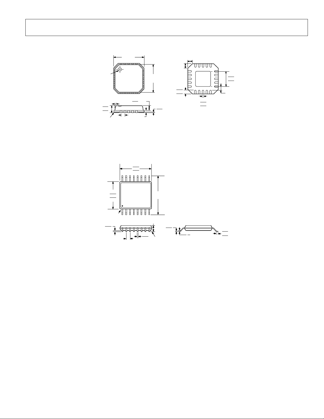
ADF4110/ADF4111/ADF4112/ADF4113
OUTLINE DIMENSIONS
0.60
MAX
0.60
MAX
0.75
0.55
0.35
COPLANARITY
0.08
16
15
11
10
BOTTOM
VIEW
0.30
0.23
0.18
20
1
2.25
2.10 SQ
1.95
5
6
0.25MIN
PIN 1
INDICATOR
1.00
0.85
0.80
SEATING
PLANE
12° MAX
BSC SQ
0.50
BSC
4.0
TOP
VIEW
0.80 MAX
0.65 TYP
0.20
REF
3.75
BSC SQ
0.05 MAX
0.02 NOM
COMPLIANT TO JEDEC STANDARDS MO-220-VGGD-1
Figure 40. 20-Lead Lead Frame Chip Scale Package [LFCSP]
(CP-20-1)
Dimensions shown in millimeters
5.10
5.00
4.90
0.15
0.05
4.50
4.40
4.30
PIN 1
16
0.65
BSC
COPLANARITY
COMPLIANT TO JEDEC STANDARDS MO-153AB
0.10
0.30
0.19
9
81
1.20
MAX
SEATING
PLANE
6.40
BSC
0.20
0.09
8°
0°
0.75
0.60
0.45
Figure 41. 16-Lead Thin Shrink Small Outline Package [TSSOP]
(RU-16)
Dimensions shown in millimeters
Rev. C | Page 27 of 28
Page 28

ADF4110/ADF4111/ADF4112/ADF4113
ORDERING GUIDE
Model Temperature Range Package Description Package Option
ADF4110BRU –40°C to +85°C Thin Shrink Small Outline Package RU-16
ADF4110BRU-REEL –40°C to +85°C Thin Shrink Small Outline Package RU-16
ADF4110BRU-REEL7 -40°C to +85°C Thin Shrink Small Outline Package RU-16
ADF4110BCP –40°C to +85°C Lead Frame Chip Scale Package CP-20
ADF4110BCP -REEL –40°C to +85°C Lead Frame Chip Scale Package CP-20
ADF4110BCP-REEL7 –40°C to +85°C Lead Frame Chip Scale Package CP-20
ADF4111BRU –40°C to +85°C Thin Shrink Small Outline Package RU-16
ADF4111BRU-REEL –40°C to +85°C Thin Shrink Small Outline Package RU-16
ADF4111BRU-REEL7 –40°C to +85°C Thin Shrink Small Outline Package RU-16
ADF4111BCP –40°C to +85°C Lead Frame Chip Scale Package CP-20
ADF4111BCP-REEL –40°C to +85°C Lead Frame Chip Scale Package CP-20
ADF4111BCP-REEL7 –40°C to +85°C Lead Frame Chip Scale Package CP-20
ADF4112BRU –40°C to +85°C Thin Shrink Small Outline Package RU-16
ADF4112BRU-REEL –40°C to +85°C Thin Shrink Small Outline Package RU-16
ADF4112BRU-REEL7 –40°C to +85°C Thin Shrink Small Outline Package RU-16
ADF4112BRUZ1 –40°C to +85°C Thin Shrink Small Outline Package RU-16
ADF4112BRUZ1-REEL –40°C to +85°C Thin Shrink Small Outline Package RU-16
ADF4112BRUZ1-REEL7 –40°C to +85°C Thin Shrink Small Outline Package RU-16
ADF4112BCP –40°C to +85°C Lead Frame Chip Scale Package CP-20
ADF4112BCP-REEL –40°C to +85°C Lead Frame Chip Scale Package CP-20
ADF4112BCP-REEL7 –40°C to +85°C Lead Frame Chip Scale Package CP-20
ADF4113BRU –40°C to +85°C Thin Shrink Small Outline Package RU-16
ADF4113BRU-REEL –40°C to +85°C Thin Shrink Small Outline Package RU-16
ADF4113BRU-REEL7 –40°C to +85°C Thin Shrink Small Outline Package RU-16
ADF4113BRUZ1 –40°C to +85°C Thin Shrink Small Outline Package RU-16
ADF4113BRUZ1-REEL –40°C to +85°C Thin Shrink Small Outline Package RU-16
ADF4113BRUZ1-REEL7 –40°C to +85°C Thin Shrink Small Outline Package RU-16
ADF4113BCP –40°C to +85°C Lead Frame Chip Scale Package CP-20
ADF4113BCP-REEL –40°C to +85°C Lead Frame Chip Scale Package CP-20
ADF4113BCP-REEL7 –40°C to +85°C Lead Frame Chip Scale Package CP-20
ADF4113BCHIPS –40°C to +85°C DIE
EVAL-ADF4112EB1 Evaluation Board
EVAL-ADF4113EB1 Evaluation Board
EVAL-ADF4113EB2 Evaluation Board
EVAL-ADF411XEB1 Evaluation Board
1
Z = Pb-free part.
Purchase of licensed I2C components of Analog Devices or one of its sublicensed Associated Companies conveys a license for the purchaser under the Philips I2C Patent
Rights to use these components in an I
© 2004 Analog Devices, Inc. All rights reserved. Trademarks and
registered trademarks are the property of their respective owners.
C03496–0–3/04(C)
2
C system, provided that the system conforms to the I2C Standard Specification as defined by Philips.
Rev. C | Page 28 of 28
 Loading...