

Page 1
High Frequency Divider/PLL Synthesizer
FEATURES
7.5 GHz bandwidth
Maximum PFD frequency of 120 MHz
Divide ratios of 8, 16, 32, or 64
2.7 V to 3.3 V power supply
V
DD
) allows
P
Separate charge pump supply (V
extended tuning voltage in 3 V systems
R
contol of charge pump current
SET
Hardware power-down mode
APPLICATIONS
Satellite communications
Broadband wireless access
CATV
Instrumentation
Wireless LANs
GENERAL DESCRIPTION
The ADF4007 is a high frequency divider/PLL synthesizer that
can be used in a variety of communications applications. It can
operate to 7.5 GHz on the RF side and to 120 MHz at the PFD.
It consists of a low noise digital PFD (phase frequency
detector), a precision charge pump, and a divider/prescaler. The
divider/ prescaler value can be set by two external control pins
to one of four values (8, 16, 32, or 64). The reference divider is
permanently set to 2, allowing an external REF
up to 240 MHz.
A complete PLL (phase-locked loop) can be implemented if the
synthesizer is used with an external loop filter and a VCO
(voltage controlled oscillator). Its very high bandwidth means
that frequency doublers can be eliminated in many high
frequency systems, simplifying system architecture and
reducing cost.
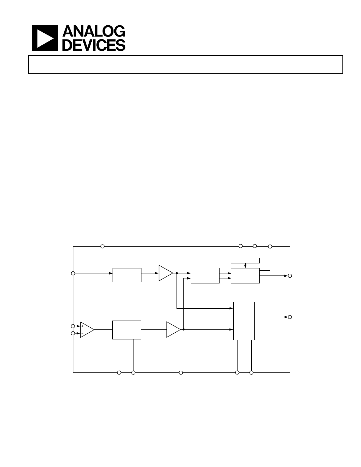
FUNCTIONAL BLOCK DIAGRAM
V
P
CPGND R
SET
ADF4007
frequency of
IN
ADF4007
REF
IN
RFINA
B
RF
IN
Rev. 0
Information furnished by Analog Devices is believed to be accurate and reliable.
However, no responsibility is assumed by Analog Devices for its use, nor for any
infringements of patents or other rights of third parties that may result from its use.
Specifications subject to change without notice. No license is granted by implication
or otherwise under any patent or patent rights of Analog Devices. Trademarks and
registered trademarks are the property of their respective owners.
R COUNTER
÷ 2
N COUNTER
÷ 8, ÷ 16,
÷ 32, ÷ 64
N2 N1 GND
Figure 1.
REFERENCE
PHASE
FREQUENCY
DETECTOR
One Technology Way, P.O. Box 9106, Norwood, MA 02062-9106, U.S.A.
Tel: 781.329.4700
Fax: 781.326.8703 © 2004 Analog Devices, Inc. All rights reserved.
CHARGE
PUMP
MUX
M2 M1
www.analog.com
CP
MUXOUT
04537-0-001
Page 2

ADF4007
TABLE OF CONTENTS
Specifications..................................................................................... 3
R Counter .......................................................................................9
Absolute Maximum Ratings............................................................ 4
ESD Caution.................................................................................. 4
Pin Configuration and Function Descriptions............................. 5
Typical Performance Characteristics ............................................. 7
Theory of Operation ........................................................................ 9
Reference Input Section............................................................... 9
RF Input Stage............................................................................... 9
Prescaler P ..................................................................................... 9
REVISION HISTORY
Revision 0: Initial Version
Phase Frequency Detector (PFD) and Charge Pump...............9
MUXOUT ................................................................................... 10
Applications..................................................................................... 11
Fixed High Frequency Local Oscillator................................... 11
Using the ADF4007 as a Divider .............................................. 12
PCB Design Guidelines for Chip Scale Package......................... 13
Outline Dimensions....................................................................... 14
Ordering Guide .......................................................................... 14
Rev. 0 | Page 2 of 16
Page 3
ADF4007
SPECIFICATIONS
AVDD = DVDD = 3 V ± 10%, AVDD ≤ VP ≤ 5.5 V, AGND = DGND = CPGND = 0 V, R
T
= T
to T
A
MAX
, unless otherwise noted.
MIN
Table 1.
Parameter B Version
1
Unit Test Conditions/Comments
RF CHARACTERISTICS
RF Input Frequency (RFIN) 1.0/7.0 GHz min/max RF input level: +5 dBm to −10 dBm
RF Input Frequency 0.5/7.5 GHz min/max RF input level: +5 dBm to −5 dBm
REFIN CHARACTERISTICS
REFIN Input Sensitivity 0.8/V
DD
V p-p min/max Biased at AVDD/2
REFIN Input Frequency 20/240 MHz min/max For f < 20 MHz, use square wave (slew rate > 50 V/µs)
REFIN Input Capacitance 10 pF max
REFIN Input Current ±100 µA max
PHASE DETECTOR
Phase Detector Frequency
3
120 MHz max
MUXOUT
MUXOUT Frequency
3
200 MHz max CL = 15 pF
CHARGE PUMP
ICP Sink/Source 5.0 mA typ With R
Absolute Accuracy 2.5 % typ With R
R
Range 3.0/11 kΩ typ
SET
ICP Three-State Leakage 10 nA max TA = 85°C
Sink and Source Current Matching 2 % typ
ICP vs. V
CP
1.5 % typ
ICP vs. Temperature 2 % typ VCP = VP/2
LOGIC INPUTS
VIH, Input High Voltage 1.4 V min
VIL, Input Low Voltage 0.6 V max
I
, I
, Input Current ±1 µA max TA = 25°C
INH
INL
CIN, Input Capacitance 10 pF max
LOGIC OUTPUTS
VOH, Output High Voltage VDD − 0.4 V min IOH = 100 µA
VOL, Output Low Voltage 0.4 V max IOL = 500 µA
POWER SUPPLIES
AV
DV
V
I
DD
I
P
DD
DD
P
4
(AI
+ DI ) 17 mA max 15 mA typ
DD DD
2.7/3.3 V min/max
AV
DD
AVDD/5.5 V min/max
2.0 mA max TA = 25°C
NOISE CHARACTERISTICS
Normalized Phase Noise Floor
5
−219 dBc/Hz typ
1
Operating temperature range (B version) is −40°C to +85°C.
2
AC coupling ensures AVDD/2 bias. See for typical circuit. Figure 13
3
Guaranteed by design. Characterized to ensure compliance.
4
TA = 25°C; AVDD = DVDD = 3 V; N = 64; RFIN = 7.5 GHz.
5
The synthesizer phase noise floor is estimated by measuring the in-band phase noise at the output of the VCO, PN
value) and 10logFPFD. PN
SYNTH
= PN
− 10logF
TOT
− 20logN. The in-band phase noise (PN
PFD
) is measured using the HP8562E Spectrum Analyzer from Agilent.
TOT
= 5.1 kΩ, dBm referred to 50 Ω,
SET
For lower frequencies, ensure that slew rate (SR) > 560 V/µs
2
= 5.1 kΩ
SET
= 5.1 kΩ
SET
0.5 V ≤ VCP ≤ VP − 0.5 V
0.5 V ≤ VCP ≤ VP − 0.5 V
≤ V
AV
≤ 5.5 V
DD
P
, and subtracting 20logN (where N is the N divider
TOT
Rev. 0 | Page 3 of 16
Page 4
ADF4007
ABSOLUTE MAXIMUM RATINGS
TA = 25°C, unless otherwise noted.
Table 2.
Parameter Rating
AVDD to GND
AVDD to DV
VP to GND −0.3 V to +5.8 V
VP to AV
Digital I/O Voltage to GND −0.3 V to VDD + 0.3 V
Analog I/O Voltage to GND −0.3 V to VP + 0.3 V
REFIN, RFINA, RFINB to GND −0.3 V to VDD + 0.3 V
Operating Temperature Range
Industrial (B Version) −40°C to +85°C
Storage Temperature Range −65°C to +125°C
Maximum Junction Temperature 150°C
CSP θJA Thermal Impedance 122°C/W
Lead Temperature, Soldering
Vapor Phase (60 s) 215°C
Infrared (15 s) 220°C
Transistor Count
CMOS 6425
Bipolar 303
1
GND = AGND = DGND = 0 V.
1
DD
DD
−0.3 V to +3.6 V
−0.3 V to +0.3 V
−0.3 V to +5.8 V
Stresses above those listed under Absolute Maximum Ratings
may cause permanent damage to the device. This is a stress
rating only; functional operation of the device at these or any
other conditions above those listed in the operational sections
of this specification is not implied. Exposure to absolute
maximum rating conditions for extended periods may affect
device reliability.
This device is a high performance RF integrated circuit with an
ESD rating of <2 kV, and it is ESD sensitive. Proper precautions
should be taken for handling and assembly.
ESD CAUTION
ESD (electrostatic discharge) sensitive device. Electrostatic charges as high as 4000 V readily accumulate on
the human body and test equipment and can discharge without detection. Although this product features
proprietary ESD protection circuitry, permanent damage may occur on devices subjected to high energy
electrostatic discharges. Therefore, proper ESD precautions are recommended to avoid performance
degradation or loss of functionality.
Rev. 0 | Page 4 of 16
Page 5
ADF4007
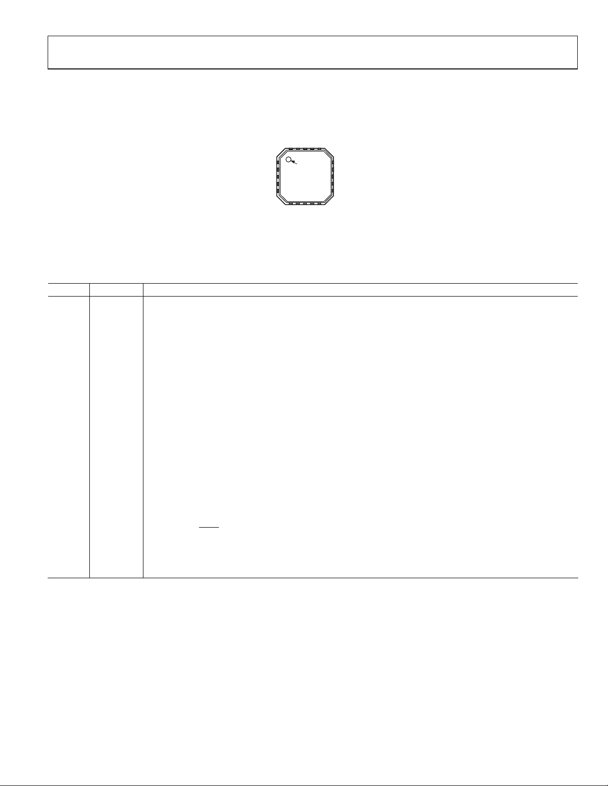
PIN CONFIGURATION AND FUNCTION DESCRIPTIONS
DD
SET
20 CP
19 R
18 VP17 DVDD16 DV
CPGND 1
AGND 2
AGND 3
RFINB4
A5
RF
IN
PIN1
INDICATOR
ADF4007
TOPVIEW
6
7
DD
DD
AV
AV
15 MUXOUT
14 M1
13 M2
12 N1
11 N2
8
IN
REF
DGND 9
DGND 10
04537-0-002
Figure 2. Pin Configuration
Table 3. Pin Function Descriptions
Pin No. Mnemonic Function
1 CPGND Charge Pump Ground. The ground return path of the charge pump.
2, 3 AGND Analog Ground. The ground return path of the prescaler.
4 RFINB
Complementary Input to the RF Prescaler. This point must be decoupled to the ground plane with a small bypass
capacitor, typically 100 pF.
5 RFINA Input to the RF Prescaler. This small signal input is ac-coupled to the external VCO.
6, 7 AV
8 REF
DD
IN
Analog Power Supply. This pin can range from 2.7 V to 3.3 V. Decoupling capacitors to the analog ground plane
should be placed as close as possible to this pin. AV
must be the same value as DVDD.
DD
Reference Input. A CMOS input with a nominal threshold of VDD/2 and a dc equivalent input resistance of 100 kΩ.
This input can be driven from a TTL or CMOS crystal oscillator, or it can be ac-coupled.
9, 10 DGND Digital Ground.
11, 12 N2, N1 These two bits set the N value. See Table 4.
13, 14 M2, M1 These two bits set the status of MUXOUT and PFD polarity. See Table 5.
15 MUXOUT This multiplexer output allows either the N divider output or the R divider output to be accessed externally.
16, 17 DV
18 V
DD
P
Digital Power Supply. This pin can range from 2.7 V to 3.3 V. Decoupling capacitors to the digital ground plane
should be placed as close as possible to this pin. DV
must be the same value as AVDD.
DD
Charge Pump Power Supply. This pin should be greater than or equal to VDD. In systems where VDD is 3 V, it can be
set to 5 V and used to drive a VCO with a tuning range of up to 5 V.
19 R
SET
20 CP
Connecting a resistor between this pin and CPGND sets the maximum charge pump output current. The nominal
voltage potential at the R
5.25
=
I
MAXCP
R
SET
Therefore, if R
= 5.1 kΩ, then ICP = 5 mA.
SET
pin is 0.66 V. The relationship between ICP and R
SET
Charge Pump Output. When enabled, this pin provides ±I
to the external loop filter, which in turn drives the
CP
is
SET
external VCO.
Rev. 0 | Page 5 of 16
Page 6

ADF4007
Table 4. N Truth Table
N2 N1 N Value
0 0 8
0 1 16
1 0 32
1 1 64
Table 5. M Truth Table
M2 M1 Operation
0 0 CP: Active
MUXOUT: V
PFD polarity: +ve
0 1 CP: Three-state
MUXOUT: R divider output
PFD polarity: +ve
1 0 CP: Active
MUXOUT: N divider output
PFD polarity: +ve
1 1 CP: Active
MUXOUT: GND
PFD polarity: −ve
DD
Rev. 0 | Page 6 of 16
Page 7

ADF4007
TYPICAL PERFORMANCE CHARACTERISTICS
Table 6. S-Parameter Data for the RF Input
Frequency
0.60000 0.87693 −19.9279
0.70000 0.85834 −23.5610
0.80000 0.85044 −26.9578
0.90000 0.83494 −30.8201
1.00000 0.81718 −34.9499
1.10000 0.80229 −39.0436
1.20000 0.78917 −42.3623
1.30000 0.77598 −46.3220
1.40000 0.75578 −50.3484
1.50000 0.74437 −54.3545
1.60000 0.73821 −57.3785
1.70000 0.72530 −60.6950
1.80000 0.71365 −63.9152
1.90000 0.70699 −66.4365
2.00000 0.70380 −68.4453
2.10000 0.69284 −70.7986
2.20000 0.67717 −73.7038
2.30000 0.67107 −75.8206
2.40000 0.66556 −77.6851
2.50000 0.65640 −80.3101
2.60000 0.63330 −82.5082
2.70000 0.61406 −85.5623
2.80000 0.59770 −87.3513
2.90000 0.56550 −89.7605
3.00000 0.54280 −93.0239
3.10000 0.51733 −95.9754
3.20000 0.49909 −99.1291
3.30000 0.47309 −102.208
3.40000 0.45694 −106.794
3.50000 0.44698 −111.659
3.60000 0.43589 −117.986
3.70000 0.42472
3.80000 0.41175
3.90000 0.41055
4.00000 0.40983
4.10000 0.40182
1
Frequency unit: GHz; parameter type: s; data format: MA; keyword: R;
impedance: 50.
1
MagS11 AngS11
Frequency
4.20000 0.41036
4.30000 0.41731
4.40000 0.43126
4.50000 0.42959
1
MagS11 AngS11
−162.939
−168.232
−174.663
−179.797
4.60000 0.42687 174.379
4.70000 0.43450 171.537
4.80000 0.42275 167.201
4.90000 0.40662 163.534
5.00000 0.39103 159.829
5.10000 0.37761 157.633
5.20000 0.34263 152.815
5.30000 0.30124 147.632
5.40000 0.27073 144.304
5.50000 0.23590 138.324
5.60000 0.17550 131.087
5.70000 0.12739 124.568
5.80000 0.09058 119.823
5.90000 0.06824 114.960
6.00000 0.04465 84.4391
6.10000 0.04376 34.2210
6.20000 0.06621 4.70571
−125.620
−133.291
−140.585
−147.970
−155.978
6.30000 0.08498
6.40000 0.10862
6.50000 0.12161
6.60000 0.12917
6.70000 0.12716
6.80000 0.11678
6.90000 0.10533
7.00000 0.09643
7.10000 0.08919
7.20000 0.08774
7.30000 0.09289
7.40000 0.10803
7.50000 0.13956
−12.6228
−26.6069
−38.5860
−47.1990
−55.8515
−63.0234
−66.9967
−75.4961
−89.2055
−103.786
−127.153
−150.582
−170.971
Rev. 0 | Page 7 of 16
Page 8

ADF4007
0
–5
–10
–15
–20
–25
–30
RF INPUT POWER (dBm)
–35
–40
0
0.5 1.0 1.5 2.0 2.5 3.0 3.5 4.0 4.5 5.0 5.5 6.0 6.5 7.0 7.5
0
REF LEVEL = –14.3dBm
–10
–20
–30
–40
–50
–60
–70
OUTPUT POWER (dB)
–80
–90
–100
TA = +25°C
RF INPUT FREQUENCY (GHz)
Figure 3. Input Sensitivity
–2k
T
V
DD
I
= 5mA
CP
PFD FREQUENCY = 106kHz
LOOP BANDWIDTH = 1MHz
RES BANDWIDTH = 10Hz
VIDEO BANDWIDTH = 10Hz
SWEEP = 1.9s
AVERAGES = 10
FREQUENCY (Hz)
TA= +85°C
= –40°C
A
= 3V, VP = 5V
–99dBc/Hz
VDD = 3V
V
= 3V
P
2k6780M–1k 1k
04537-0-003
04537-0-005
0
REF LEVEL = –14.0dBm
–10
–20
–30
–40
–50
–60
–70
OUTPUT POWER (dB)
–80
–90
–100
–212 2126780–106 106
FREQUENCY (MHz)
Figure 6. Reference Spurs (6.78 GHz RF
and 1 MHz Loop Bandwidth)
–120
–130
–140
–150
–160
PHASE NOISE (dBc/Hz)
–170
–180
10k
100k 1M 10M
PHASE DETECTOR FREQUENCY (Hz)
V
= 3V, VP = 5V
DD
= 5mA
I
CP
PFD FREQUENCY = 106MHz
LOOP BANDWIDTH = 1MHz
RES BANDWIDTH = 1kHz
VIDEO BANDWIDTH = 1kHz
SWEEP = 2.5s
AVERAGES = 30
–91.0dBc/Hz
, 106 MHz PFD,
OUT
VDD = 3V
V
= 5V
P
120M
04537-0-007
04537-0-013
Figure 4. Phase Noise (6.78 GHz RF
and 1 MHz Loop Bandwidth)
–40
–50
–60
–70
–80
–90
–100
–110
PHASE NOISE (dBc/Hz)
–120
–130
–140
10k 100M
100k 1M 10M
FREQUENCY OFFSET FROM CARRIER (Hz)
Figure 5. Integrated Phase Noise (6.78 GHz RF
and 1 MHz Loop Bandwidth)
, 106 MHz PFD,
OUT
10dB/DIV
= –40dBc/Hz
R
L
RMS NOISE = 4.2°
, 106 MHz PFD,
OUT
04537-0-006
Rev. 0 | Page 8 of 16
Figure 7. Phase Noise (Referred to CP Output) vs. PFD Frequency
–6
–5
–4
–3
–2
–1
0
(mA)
CP
I
1
2
3
4
5
6
0 2.00.5 1.0 1.5
V
(V)
CP
Figure 8. Charge Pump Output Characteristics
VP = 5V
= 5mA
I
CP
4.02.5 3.0 3.5 5.04.5
04537-0-014
Page 9

ADF4007
THEORY OF OPERATION
REFERENCE INPUT SECTION
The reference input stage is shown in Figure 9. SW1 and SW2
are normally closed switches. SW3 is normally open. When
power-down is initiated, SW3 is closed and SW1 and SW2 are
opened. This ensures that there is no loading of the REF
on power-down.
POWER-DOWN
CONTROL
100kΩ
NC
SW1
SW2
BUFFER
REF
IN
NC
pin
IN
TO R COUNTER
PRESCALER P
The prescaler, operating at CML levels, takes the clock from the
RF input stage and divides it down to a manageable frequency
for the PFD. The prescaler can be selected to be either 8, 16, 32,
or 64, and is effectively the N value in the PLL synthesizer. The
terms N and P are used interchangeably in this data sheet. N1
and N2 set the prescaler values. The prescaler value should be
chosen so that the prescaler output frequency is always less than
or equal to 120 MHz, the maximum specified PFD frequency.
Thus, with an RF frequency of 4 GHz, a prescaler value of 64 is
valid, but a value of 32 or less is not valid.
f
REFIN
VCO
×=
][
Nf
2
SW3
NO
Figure 9. Reference Input Stage
RF INPUT STAGE
The RF input stage is shown in Figure 10 . It is followed by a
2-stage limiting amplifier to generate the CML clock levels
needed for the prescaler.
BIAS
GENERATOR
A
RF
IN
B
RF
IN
Figure 10. RF Input Stage
500Ω
1.6V
500Ω
AV
AGND
DD
04537-0-016
04537-0-015
R COUNTER
The R counter is permanently set to 2. It allows the input
reference frequency to be divided down by 2 to produce the
reference clock to the phase frequency detector (PFD).
PHASE FREQUENCY DETECTOR (PFD) AND CHARGE PUMP
The PFD takes inputs from the R counter and the N counter
(prescaler, P) and produces an output proportional to the phase
and frequency difference between them. Figure 11 is a
simplified schematic. The PFD includes a fixed, 3 ns delay
element that controls the width of the antibacklash pulse. This
pulse ensures that there is no dead zone in the PFD transfer
function and minimizes phase noise and reference spurs.
V
P
CHARGE
PUMP
CP
LOGIC HI
R DIVIDER
D1
U1
CLR1
UP
Q1
3ns
DELAY
U3
N DIVIDER
Rev. 0 | Page 9 of 16
CLR2
LOGIC HI
DOWN
D2
Q2
U2
Figure 11. PFD Simplified Schematic and Timing (In Lock)
CPGND
04537-0-017
Page 10

ADF4007
MUXOUT
The output multiplexer on the ADF4007 allows the user to
access various internal points on the chip. The state of
MUXOUT is controlled by the M2 and M1 pins. Figure 12
shows the MUXOUT section in block diagram form.
DV
DD
DV
DD
R COUNTER OUTPUT
N COUNTER OUTPUT
DGND
MUX
CONTROL
MUXOUT
PFD Polarity
The PFD polarity is set by the state of M2 and M1 pins as given
in the Table 5. The ability to set the polarity allows the use of
VCOs with either positive or negative tuning characteristics. For
standard VCOs with positive characteristics (output frequency
increases with increasing tuning voltage), the polarity should be
set to positive. This is accomplished by tying M2 and M1 to a
logic low state.
CP Output
The CP output state is also controlled by the state of M2 and
M1. It can be set either to active (so that the loop can be locked)
or to three-state (open the loop). The normal state is CP output
active.
DGND
Figure 12. MUXOUT Circuit
04537-0-018
Rev. 0 | Page 10 of 16
Page 11

ADF4007
APPLICATIONS
FIXED HIGH FREQUENCY LOCAL OSCILLATOR
Figure 13 shows the ADF4007 being used with the
HMC358MS8G VCO from Hittite Microwave Corporation to
produce a fixed-frequency LO (local oscillator), which could be
used in satellite or CATV applications. In this case, the desired
LO is 6.7 GHz.
The reference input signal is applied to the circuit at FREF
IN
and, in this case, is terminated in 50 Ω. Many systems would
have either a TCXO or an OCXO driving the reference input
without any 50 Ω termination. To bias the REF
pin at AVDD/2,
IN
ac coupling is used. The value of the coupling capacitor used
depends on the input frequency. The equivalent impedance at
the input frequency should be less than 10 Ω. Given that the dc
input impedance at the REF
pin is 100 kΩ, less than 0.1% of
IN
the signal is lost.
The charge pump output of the ADF4007 drives the loop filter.
In calculating the loop filter component values, a number of
items need to be considered. In this example, the loop filter was
designed so that the overall phase margin for the system is 45°.
Other PLL system specifications are as follows:
= 5 mA
K
D
K
= 100 MHz/V
V
Loop Bandwidth = 300 kHz
= 106 MHz
F
PFD
N = 64
All these specifications are needed and used with the
ADIsimPLL to derive the loop filter component values shown in
Figure 13.
The circuit in Figure 13 gives a typical phase noise performance
of −100 dBc/Hz at 10 kHz offset from the carrier. Spurs are
heavily attenuated by the loop filter and are below −90 dBc.
The loop filter output drives the VCO, which, in turn, is fed
back to the RF input of the PLL synthesizer and also drives the
RF output terminal. A T-circuit configuration provides 50 Ω
matching between the VCO output, the RF output, and the RF
IN
terminal of the synthesizer.
FREF
100pF 100pF
IN
51Ω
AVDD = 3.3V
7
16
DV
17
DV
DD
DD
AV
DD
B
5
4
6
AV
RFINA
RF
DD
IN
ADF4007
8
REF
IN
LOGIC HI
LOGIC HI
LOGIC LO
LOGIC LO
5.1kΩ
11
N2
12
N1
13
M2
14
M1
R
19
SET
R
SET
GND
NOTE
DECOUPLING CAPACITORS (0.1mF/10pF) ON AV
OF THE AD820 AND THE HMC358MS8G HAVE BEEN OMITTED FROM THE DIAGRAM
V
CC
TO AID CLARITY.
MUXOUT
GND
32
18kΩ
22Ω
47nF
VCC = 12V
AD820
1kΩ
10pF
GND
GND
9
18
V
P
CP
1kΩ
20
5.6nF
15
10
100pF
, DVDD, AND VP OF THE ADF4007 AND ON
DD
Figure 13. 6.78 GHz Local Oscillator Using the ADF4007
V
= 3.3V
CC
HMC358MS8G
VCO
100MHz/V
100pF
18Ω
18Ω
18Ω
100pF
RF
OUT
04537-0-019
Rev. 0 | Page 11 of 16
Page 12

ADF4007
USING THE ADF4007 AS A DIVIDER
In addition to its use as a standard PLL synthesizer, the
ADF4007 can also be used as a high frequency counter/divider
with a value of 8, 16, 32, or 64.This can prove useful in a wide
variety of applications where a higher frequency signal is readily
available. Figure 14 shows the ADF4007 used in this manner
with the ADF4360-7.
FREF
SPI COMPATIBLE SERIAL BUS
IN
1nF
10µF
14
C
1nF
1nF
16
REF
51Ω
17
18
19
12
13
4.7kΩ
CPGND AGND DGND
N
CLK
DATA
LE
C
C
R
SET
1
V
V
VCO
6
V
VCO
IN
DD
2
21
DV
AV
DD
ADF4360-7
22
11
8
3
DD
CE
15
2.2nH
23
LOCK
DETECT
MUXOUT
L1
9
20
V
7
TUNE
24
CP
470pF
V
VCO
51Ω
4
RF
A
OUT
L2
10
2.2nH
5
RF
B
OUT
13kΩ
6.8nF
6.2kΩ
This part is an integrated synthesizer and VCO, in this case
operating over a range of 1200 MHz to 1500 MHz. With divideby-8 chosen in the ADF4007 (N2 = 0, N1 = 0), the output range
is 150 MHz to 187.50 MHz.
V
DD
220pF
51Ω
100pF
100pF
4.7kΩ
REF
RFINA
RFINB
R
SET
CHARGE
PUMP
IN
R COUNTER
CPGND
CP
÷2
GND
V
PAVDD
PHASE
FREQUENCY
DETECTOR
DV
DD
NCOUNTER
÷8, ÷16
÷32, ÷64
N1
N2
M2 M1
MUX
ADF4007
MUXOUT
CMOS OUTPUT
04537-0-020
Figure 14. Using the ADF4007 to Divide-Down the Output of the ADF4360-7
Rev. 0 | Page 12 of 16
Page 13

ADF4007
PCB DESIGN GUIDELINES FOR CHIP SCALE PACKAGE
The lands on the chip scale package (CP-20) are rectangular.
The printed circuit board pad for these should be 0.1 mm
longer than the package land length and 0.05 mm wider than
the package land width. The land should be centered on the pad
to ensure that the solder joint size is maximized.
The bottom of the chip scale package has a central thermal pad.
The thermal pad on the printed circuit board should be at least
as large as this exposed pad. The printed circuit board should
have a clearance of at least 0.25 mm between the thermal pad
and the inner edges of the pad pattern to ensure that shorting is
avoided.
Thermal vias may be used on the printed circuit board thermal
pad to improve thermal performance of the package. If vias are
used, they should be incorporated in the thermal pad at 1.2 mm
pitch grid. The via diameter should be between 0.30 mm and
0.33 mm, and the via barrel should be plated with 1 oz. copper
to plug the via.
The user should connect the printed circuit board thermal pad
to AGND.
Rev. 0 | Page 13 of 16
Page 14

ADF4007
OUTLINE DIMENSIONS
INDICATOR
SEATING
PIN 1
1.00
0.85
0.80
PLANE
12° MAX
BSC SQ
0.50
BSC
4.0
TOP
VIEW
0.80 MAX
0.65 TYP
0.20
REF
3.75
BSC SQ
0.05 MAX
0.02 NOM
0.60
MAX
0.60
MAX
0.75
0.55
0.35
COPLANARITY
0.08
16
15
11
10
BOTTOM
VIEW
0.30
0.23
0.18
20
1
2.25
2.10 SQ
1.95
5
6
0.25MIN
COMPLIANT TO JEDEC STANDARDS MO-220-VGGD-1
Figure 15. 20-Lead Frame Chip Scale Package [LFCSP]
(CP-20)
Dimensions shown in millimeters
ORDERING GUIDE
Model Temperature Range Package Description Package Option
ADF4007BCP −40°C to + 85°C 20-lead frame chip scale package (LFCSP) CP-20
ADF4007BCP–REEL −40°C to + 85°C 20-lead frame chip scale package (LFCSP) CP-20
ADF4007BCP–REEL7 −40°C to + 85°C 20-lead frame chip scale package (LFCSP) CP-20
CP = chip scale package.
Rev. 0 | Page 14 of 16
Page 15

ADF4007
NOTES
Rev. 0 | Page 15 of 16
Page 16

ADF4007
NOTES
© 2004 Analog Devices, Inc. All rights reserved. Trademarks and
registered trademarks are the property of their respective owners.
D04537–0–2/04(0)
Rev. 0 | Page 16 of 16
 Loading...