

Page 1
Single Phase, Multifunction Metering IC
Data Sheet
FEATURES
Measures active, reactive, and apparent energy; sampled
waveform; current and voltage rms
Provides a second current input for neutral current
measurement
Less than 0.1% error in active and reactive energy
measurements over a dynamic range of 3000:1
Less than 0.2% error in instantaneous IRMS measurement
over a dynamic range of 1000:1
Provides apparent energy measurement and instantaneous
power readings
1.23 kHz bandwidth operation
Flexible PGA gain stage (up to ×22)
Includes internal integrators for use with Rogowski coil sensors
2
SPI, I
C, or UART communication
GENERAL DESCRIPTION
The ADE7953 is a high accuracy electrical energy measurement
IC intended for single phase applications. It measures line voltage
and current and calculates active, reactive, and apparent energy,
as well as instantaneous rms voltage and current.
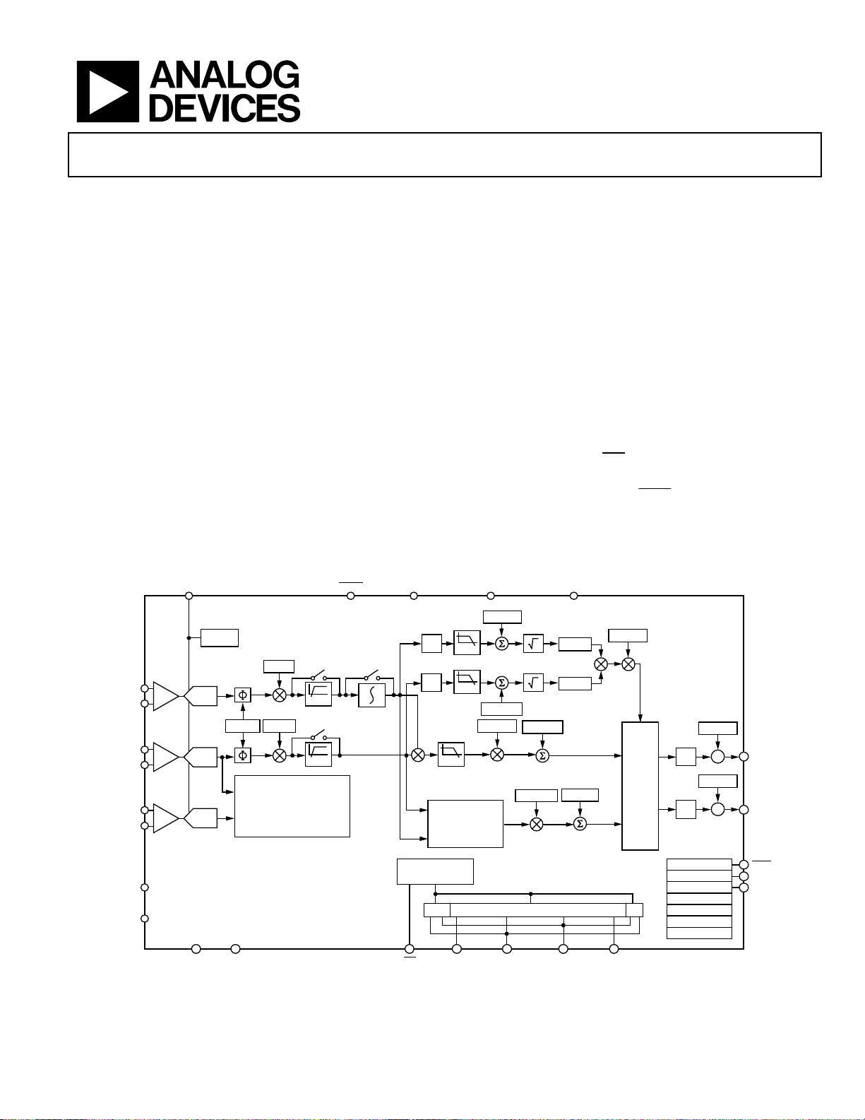
FUNCTIONAL BLOCK DIAGRAM
REF RESET VDD VINTA VINTD
with Neutral Current Measurement
ADE7953
The device incorporates three Σ- ADCs with a high accuracy
energy measurement core. The second input channel simultaneously measures neutral current and enables tamper detection
and neutral current billing. The additional channel incorporates
a complete signal path that allows a full range of measurements.
Each input channel supports independent and flexible gain stages,
making the device suitable for use with a variety of current sensors
such as current transformers (CTs) and low value shunt resistors.
Two on-chip integrators facilitate the use of Rogowski coil sensors.
The ADE7953 provides access to on-chip meter registers via a
variety of communication interfaces including SPI, I
Two configurable low jitter pulse output pins provide outputs that
are proportional to active, reactive, or apparent energy, as well as
current and voltage rms. A full range of power quality information
such as overcurrent, overvoltage, peak, and sag detection are
accessible via the external
IRQ
pin. Independent active, reactive,
and apparent no-load detections are included to prevent “meter
creep.” Dedicated reverse power (
REVP
), zero-crossing voltage
(ZX), and zero-crossing current (ZX_I) pins are also provided. The
ADE7953 energy metering IC operates from a 3.3 V supply voltage
and is available in a 28-lead LFCSP package.
2
C, and UART.
1.2V REF
LOW
NOISE
PRE-AMP
IAP
IAN
VP
VN
IBP
IBN
AGND
DGND
Rev. A
Information furnished by Analog Devices is believed to be accurate and reliable. However, no
responsibility is assumed by Anal og Devices for its use, nor for any infringements of patents or ot her
rights of third parties that may result from its use. Specifications subject to change without notice. No
license is granted by implication or otherwise under any patent or patent rights of Analog Devices.
Trademarks and registered trademarks are the property of their respective owners.
PGA
PGA
PGA
ADC
ADC
ADC
CLKIN
CLKOUT
AIGAIN
HPF
VGAINAPHCAL
HPF
ACTIVE, REACT IVE AND
APPARENT ENERGIES AND
VOLTAGE/CURRENT RMS
CALCULATION F OR PHASE B
(SEE PHASE A FOR DETAILED
DATA PATH).
DIGITAL
INTEGRATOR
CONFIGURATIO N
AND CONTROL
IRQ
AIRMSOS
2
X
LPF
2
X
LPF
VRMSOS
AWG AIN
LPF
AVARGAIN
COMPUTATIONAL
BLOCK FOR TOTAL
REACTIVE PO WER
UART SPI INT ERFACE
CS SCLK
MISO/
SDA/Tx
AWATTOS
AVR MS
MOSI/
SCL/Rx
AIRMS
AVAROS
AVAGAIN
PHASE
A AND B
DATA
2
I
C
ADE7953
CF1DEN
DFC
:
CF2DEN
DFC
:
REVP
ZX
ZX_I
PEAK
ANGLE
POWER FACTOR
SAG
Figure 1.
One Technology Way, P.O. Box 9106, Norwood, MA 02062-9106, U.S.A.
Tel: 781.329.4700 www.analog.com
Fax: 781.461.3113 ©2011 Analog Devices, Inc. All rights reserved.
CF1
CF2
REVP
ZX
ZX_I
09320-001
Page 2

ADE7953 Data Sheet
TABLE OF CONTENTS
Features.............................................................................................. 1
General Description ......................................................................... 1
Functional Block Diagram .............................................................. 1
Revision History ............................................................................... 3
Specifications..................................................................................... 4
Timing Characteristics ................................................................ 6
Absolute Maximum Ratings............................................................ 8
ESD Caution.................................................................................. 8
Pin Configuration and Function Descriptions............................. 9
Typical Performance Characteristics ........................................... 11
Test Circuit ...................................................................................... 16
Terminology .................................................................................... 17
ADE7953 Power-Up Procedure.................................................... 18
Required Register setting .......................................................... 18
Theory of Operation ...................................................................... 19
Analog Inputs.............................................................................. 19
Analog-to-Digital Conversion.................................................. 19
Current Channel ADCs............................................................ 21
Voltage Channel ADC ............................................................... 21
Reference Circuit........................................................................ 22
Root Mean Square Measurement ................................................. 23
Current Channel RMS Calculation.......................................... 23
Voltage Channel RMS Calculation........................................... 23
Active Power Calculation ..............................................................24
Sign of Active Power Calculation............................................. 24
Active Energy Calculation......................................................... 25
Active Energy Accumulation Modes....................................... 27
Reactive Power Calculation........................................................... 28
Sign of Reactive Power Calculation ......................................... 28
Reactive Energy Calculation ..................................................... 29
Reactive Energy Accumulation Modes ................................... 30
Apparent Power Calculation ......................................................... 31
Apparent Energy Calculation ................................................... 31
Ampere-Hour Accumulation.................................................... 32
Energy-to-Frequency Conversion................................................ 33
Pulse Output Characteristics ....................................................33
Energy Calibration ......................................................................... 34
Gain Calibration......................................................................... 34
Phase Calibration ....................................................................... 34
Offset Calibration....................................................................... 35
Period Measurement...................................................................... 36
Instantaneous Powers and Waveform Sampling........................ 37
Power Factor.................................................................................... 38
Using the Line Cycle Accumulation Mode to Determine the
Power Factor ............................................................................... 38
Power Factor with No-Load Detection ................................... 38
Angle Measurement................................................................... 39
No-Load Detection ........................................................................ 40
Setting the No-Load Thresholds .............................................. 40
Active Energy No-Load Detection........................................... 40
Reactive Energy No-Load Detection ....................................... 41
Apparent Energy No-Load Detection ..................................... 41
Zero-Crossing Detection............................................................... 43
Zero-Crossing Output Pins....................................................... 43
Zero-Crossing Interrupts.......................................................... 43
Zero-Crossing Timeout............................................................. 44
Zero-Crossing Threshold.......................................................... 44
Voltage Sag Detection .................................................................... 45
Setting the SAGCYC Register................................................... 45
Setting the SAGLVL Register.................................................... 45
Voltage Sag Interrupt ................................................................. 45
Peak Detection................................................................................ 46
Indication of Power Direction ...................................................... 47
Reverse Power............................................................................. 47
Sign Indication............................................................................ 47
Overcurrent and Overvoltage Detection..................................... 48
Setting the OVLVL and OILVL Registers ............................... 48
Overvoltage and Overcurrent Interrupts................................ 48
Alternative Output Functions....................................................... 49
ADE7953 Interrupts....................................................................... 50
Primary Interrupts (Voltage Channel and Current Channel
A).................................................................................................. 50
Current Channel B Interrupts .................................................. 50
Communicating with the ADE7953 ............................................ 51
Communication Autodetection ............................................... 51
Locking the Communication Interface................................... 51
SPI Interface................................................................................ 52
I2C Interface ................................................................................ 53
UART Interface........................................................................... 55
Communication Verification and Security ................................. 57
Rev. A | Page 2 of 68
Page 3

Data Sheet ADE7953
Write Protection ..........................................................................57
Communication Verification.....................................................57
Checksum Register .....................................................................58
ADE7953 Registers .........................................................................60
REVISION HISTORY
11/11—Rev. 0 to Rev. A
Changes to Figure 1...........................................................................1
Changes to Table 1 ............................................................................3
Changes to Absolute Maximum Ratings Section..........................8
Changes to Table 5 ............................................................................9
Replaced Typical Performance Characteristics Section.............11
Changes to Figure 35 ......................................................................16
Added ADE7953 Power-Up Procedure Section..........................18
Changes to Voltage Channel Section............................................19
Changes to Current Channel RMS Calculation Section and
Voltage Channel RMS Calculation Section .................................23
Changes to Active Power Calculation Section ............................24
Changes to Active Energy Integration Time Under Steady
Load Section.....................................................................................25
ADE7953 Register Descriptions ...............................................62
Outline Dimensions........................................................................68
Ordering Guide...........................................................................68
Changes to Reactive Power Calculation Section ........................28
Changes to Reactive Energy Integration Time Under Steady
Load Section ....................................................................................29
Changes to Figure 65 ......................................................................47
Changes to Write Protection Section ...........................................57
Replaced Checksum Register Section and added Figure 75 and
Figure 76...........................................................................................58
Changes to Table 12 ........................................................................59
Changes to Table 14 ........................................................................60
Changes to Table 15 ........................................................................61
Replaced Interrupt Enable Section and Interrupt Status
Registers Section .............................................................................66
2/11—Revision 0: Initial Version
Rev. A | Page 3 of 68
Page 4

ADE7953 Data Sheet
SPECIFICATIONS
VDD = 3.3 V ± 10%, AGND = DGND = 0 V, on-chip reference, CLKIN = 3.58 MHz, T
set to 0x30, unless otherwise noted.
Table 1.
Parameter Min Typ Max Unit Test Conditions/Comments
PHASE ERROR BETWEEN CHANNELS Line frequency = 45 Hz to 65 Hz, HPF on
Power Factor = 0.8 Capacitive ±0.05 Degrees Phase lead 37°
Power Factor = 0.5 Inductive ±0.05 Degrees Phase lag 60°
ACTIVE ENERGY MEASUREMENT
Active Energy Measurement Error
(Current Channel A)
Active Energy Measurement Error
(Current Channel B)
AC Power Supply Rejection VDD = 3.3 V ± 120 mV rms, 100 Hz
Output Frequency Variation 0.01 %
DC Power Supply Rejection VDD = 3.3 V ± 330 mV dc
Output Frequency Variation 0.01 %
Active Energy Measurement Bandwidth 1.23 kHz −3 db
REACTIVE ENERGY MEASUREMENT
Reactive Energy Measurement Error
(Current Channel A)
Reactive Energy Measurement Error
(Current Channel B)
AC Power Supply Rejection VDD = 3.3 V ± 120 mV rms, 100 Hz
Output Frequency Variation 0.01 %
DC Power Supply Rejection VDD = 3.3 V ± 330 mV dc
Output Frequency Variation 0.01 %
Reactive Energy Measurement
Bandwidth
RMS MEASUREMENT
IRMS and VRMS Measurement
Bandwidth
IRMS (Current Channel A) Measurement
Error
IRMS (Current Channel B) and VRMS
Measurement Error
ANALOG INPUTS
Maximum Signal Levels ±500 mV peak Differential inputs: IAP to IAN, IBP to IBN
±500 mV peak Single-ended input: VP to VN, IBP to IBN
±250 mV peak Single-ended input: IAP to IAN
Input Impedance (DC)
IAP Pin 50 MΩ
IAN Pin 50 MΩ
IBP, IBN, VP, VN Pins 540 kΩ
ADC Offset Error
Current Channel B, Voltage Channel 0 ±10 mV
Current Channel A −12 mV PGA = 1
−1 mV PGA = 16, PGA = 22
Gain Error External 1.2 V reference
Current Channel A ±3 %
Current Channel B ±3 %
Voltage Channel ±3 %
0.1 %
0.1 %
0.1 %
0.1 %
1.23 kHz −3 db
1.23 kHz
0.2 %
0.2 %
MIN
to T
= −40°C to +85°C, Register Address 0x120
MAX
Over a dynamic range of 3000:1, PGA = 1,
PGA = 22, integrator off
Over a dynamic range of 1000:1, PGA = 1,
PGA = 16, integrator off
Over a dynamic range of 3000:1, PGA = 1,
PGA = 22, integrator off
Over a dynamic range of 1000:1, PGA = 1,
PGA = 16, integrator off
Over a dynamic range of 1000:1, PGA = 1,
PGA = 22, integrator off
Over a dynamic range of 500:1, PGA = 1,
PGA = 16, integrator off
Uncalibrated error (see the Terminology
section)
Rev. A | Page 4 of 68
Page 5

Data Sheet ADE7953
Parameter Min Typ Max Unit Test Conditions/Comments
ANALOG PERFORMANCE
Signal-to-Noise Ratio
Current Channel A 74 dB
Current Channel B 72 dB
Voltage Channel 70
Signal-to-Noise-and-Distortion Ratio
Current Channel A, Current Channel B 68 dB
Voltage Channel 65 dB
Bandwidth (−3 dB) 1.23 kHz
CF1 AND CF2 PULSE OUTPUTS
Maximum Output Frequency 206.9 kHz
Duty Cycle 50 % CF1 or CF2 frequency > 6.25 Hz
Active Low Pulse Width 80 ms CF1 or CF2 frequency < 6.25 Hz
Jitter 0.04 % CF1 or CF2 frequency = 1 Hz
Output High Voltage, VOH 2.4 V I
Output Low Voltage, VOL 0.4 V I
REFERENCE Nominal 1.2 V at REF pin
REF Input Voltage Range 1.19 1.2 1.21 V T
Input Capacitance 10 pF
Reference Error ±0.9 mV TA = 25°C
Output Impedance 1.2 kΩ
Temperature Coefficient 10 50 ppm/°C
CLKIN/CLKOUT PINS All specifications CLKIN = 3.58 MHz
Input Clock Frequency 3.58 MHz
Crystal Equivalent Series Resistance 30 200 Ω
LOGIC INPUTS—RESET, CLKIN, CS, SCLK,
MOSI/SCL/Rx, MISO/SDA/Tx
Input High Voltage, V
Input Low Voltage, V
2.4 V VDD = 3.3 V ± 10%
INH
0.8 V VDD = 3.3 V ± 10%
INL
Input Current, IIN V
MOSI/SCL/Rx, MISO/SDA/Tx, RESET
−10 μA
CS, SCLK 1 μA
Input Capacitance, CIN 10 pF
LOGIC OUTPUTS—IRQ, REVP, ZX, ZX_I,
VDD = 3.3 V ± 10%
CLKOUT, MOSI/SCL/Rx, MISO/SDA/Tx
Output High Voltage, VOH 3.0 V I
Output Low Voltage, VOL 0.4 V I
POWER SUPPLY For specified performance
VDD 3.0 V 3.3 V − 10%
3.6 V 3.3 V + 10%
IDD 7 9 mA
= 500 μA at 25°C
SOURCE
= 8 mA at 25°C
SINK
to T
Max
= 0 V
= 800 μA
= 2 mA
MIN
IN
SOURCE
SINK
Rev. A | Page 5 of 68
Page 6
ADE7953 Data Sheet
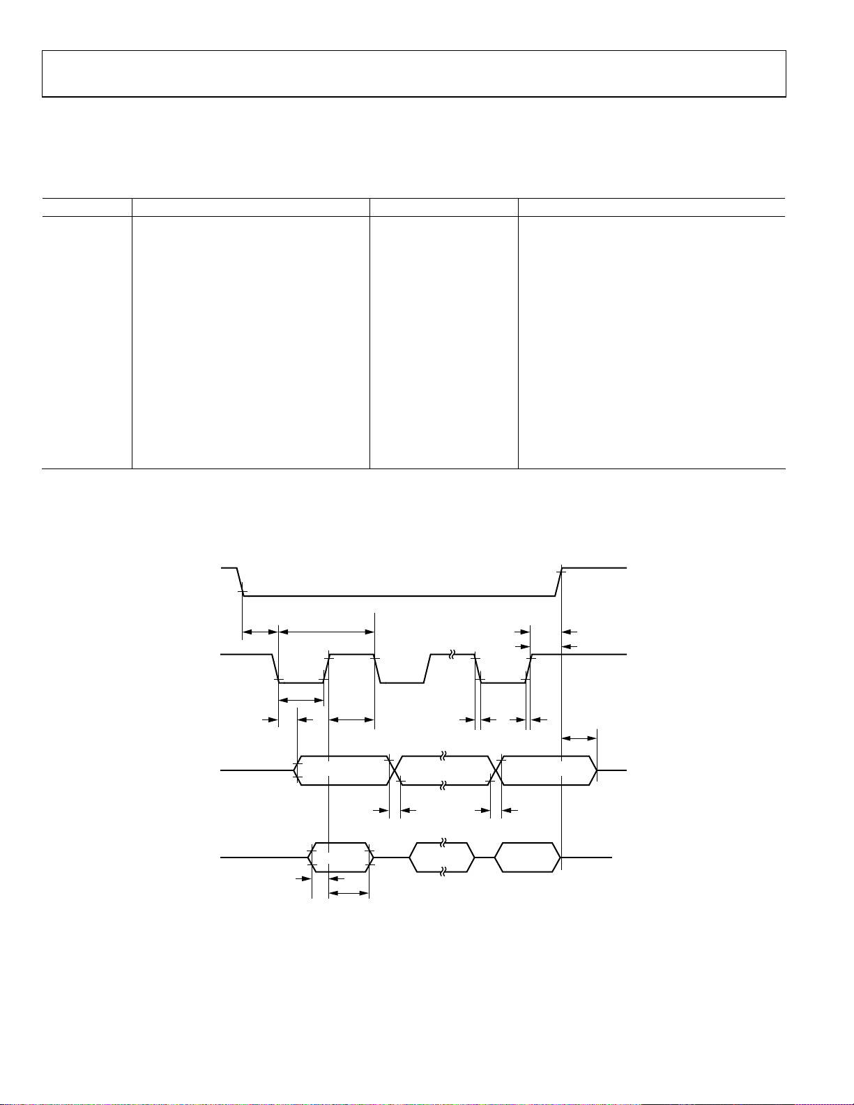
TIMING CHARACTERISTICS
SPI Interface Timing
VDD = 3.3 V ± 10%, AGND = DGND = 0 V, on-chip reference, CLKIN = 3.58 MHz, T
Table 2.
Parameter Description Min1 Max1 Unit
tCS CS to SCLK edge 50 ns
t
SCLK period 200 ns
SCLK
tSL SCLK low pulse width 80 ns
tSH SCLK high pulse width 80 ns
t
Data output valid after SCLK edge 80 ns
DAV
t
Data input setup time before SCLK edge 70 ns
DSU
t
Data input hold time after SCLK edge 5 ns
DHD
tDF Data output fall time 20 ns
tDR Data output rise time 20 ns
tSR SCLK rise time 20 ns
tSF SCLK fall time 20 ns
t
MISO disabled after CS rising edge 5 40 ns
DIS
t
CS high after SCLK edge 0 ns
SFS
t
SFS_LK
CS high after SCLK edge (when writing to
1200 ns
COMM_LOCK bit)
1
Min and max values are typical minimum and maximum values.
SPI Interface Timing Diagram
MIN
to T
= −40°C to +85°C, unless otherwise noted.
MAX
CS
SCLK
MISO
MOSI
t
CS
t
DAV
t
SCLK
t
SL
t
SH
MSB OUT LSB OUT
MSB IN
t
DSU
t
DHD
INTERMEDIATE BITS
t
DF
INTERMEDIATE BITS
t
SFS_LK
t
SFS
t
DR
LSB IN
t
SR
t
DIS
09320-003
t
SF
Figure 2. SPI Interface Timing
Rev. A | Page 6 of 68
Page 7

Data Sheet ADE7953
I2C Interface Timing
VDD = 3.3 V ± 10%, AGND = DGND = 0 V, on-chip reference, CLKIN = 3.58 MHz, T
Table 3.
Standard Mode Fast Mode
Parameter Description Min1 Max1 Min1 Max1 Unit
f
SCL clock frequency 0 100 0 400 kHz
SCL
t
Hold time for a start or repeated start condition 4.0 0.6 μs
HD;STA
t
Low period of SCL clock 4.7 1.3 μs
LOW
t
High period of SCL clock 4.0 0.6 μs
HIGH
t
Setup time for a repeated start condition 4.7 0.6 μs
SU;STA
t
Data hold time 0 3.45 0 0.9 μs
HD;DAT
t
SU;DAT
Data setup time 250 100 ns
tR Rise time of SDA and SCL signals 1000 20 300 ns
tF Fall time of SDA and SCL signals 300 20 300 ns
t
SU;STO
t
Bus-free time between a stop and start condition 4.7 1.3 μs
BUF
Setup time for stop condition 4.0 0.6 μs
tSP Pulse width of suppressed spikes N/A 50 ns
1
Min and max values are typical minimum and maximum values.
I2C Interface Timing Diagram
MIN
to T
= −40°C to +85°C, unless otherwise noted.
MAX
SDA
t
STOP
BUF
START
CONDITION
09320-002
SCL
CONDITION
START
t
F
t
t
LOW
HD;STA
t
HD;DAT
t
SU;DAT
t
R
t
HIGH
t
F
t
SU;STA
Figure 3. I
REPEATED START
CONDITIO N
2
C Interface Timing
t
HD;STA
t
SP
t
SU;STO
t
R
CONDITION
Rev. A | Page 7 of 68
Page 8
ADE7953 Data Sheet
ABSOLUTE MAXIMUM RATINGS
TA = 25°C, unless otherwise noted.
Table 4.
Parameter Rating
VDD to AGND −0.3 V to +3.7 V
VDD to DGND −0.3 V to +3.7 V
Analog Input Voltage to AGND,
IAP, IAN, IBP, IBN, VP, VN
Reference Input Voltage to AGND −0.3 V to VDD + 0.3 V
Digital Input Voltage to DGND −0.3 V to VDD + 0.3 V
Digital Output Voltage to DGND −0.3 V to VDD + 0.3 V
Operating Temperature
Industrial Range −40°C to +85°C
Storage Temperature Range −65°C to +150°C
Note that regarding the temperature profile used in soldering
RoHS-compliant parts, Analog Devices, Inc., advises that reflow
profiles should conform to J-STD 20 from JEDEC. Refer to the
JEDEC website for the latest revision.
−2 V to +2 V
Stresses above those listed under Absolute Maximum Ratings
may cause permanent damage to the device. This is a stress
rating only; functional operation of the device at these or any
other conditions above those indicated in the operational
section of this specification is not implied. Exposure to absolute
maximum rating conditions for extended periods may affect
device reliability.
ESD CAUTION
Rev. A | Page 8 of 68
Page 9
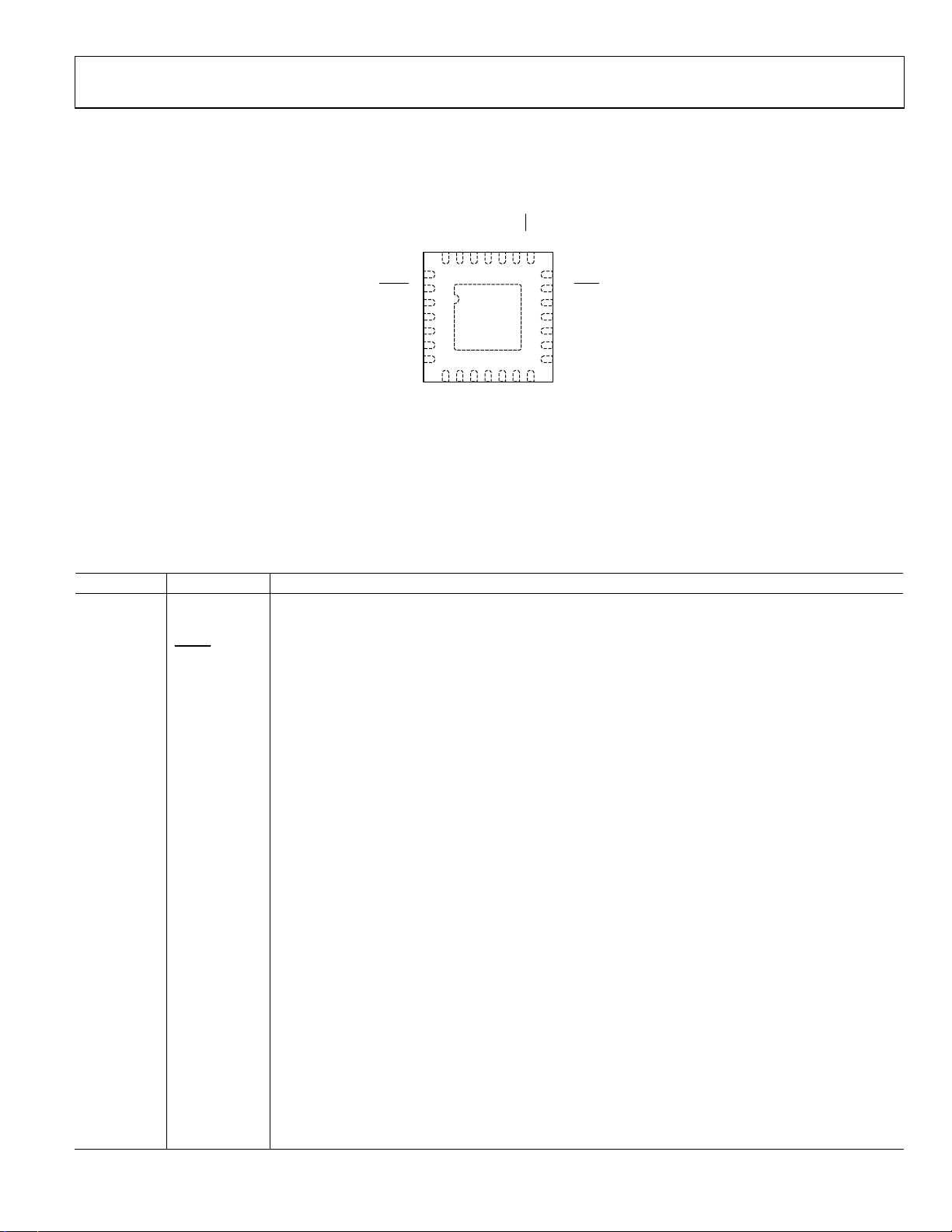
Data Sheet ADE7953
A
x
x
PIN CONFIGURATION AND FUNCTION DESCRIPTIONS
K
OSI/SCL/R
M
CS
27
28
CF1
IRQ
CF2
SCL
MISO/SDA/T
23
22
24
25
26
13
REF
14
PULL_LOW
21 ZX_I
20 REVP
19 CLKOUT
18 CLKIN
17 VDD
16 AGND
15 VINTA
09320-004
1ZX
2RESET
3VINTD
4DGND
5IAP
6IAN
7PULL_HIGH
NOTES
1. CREATE A SIMILAR PAD ON THE PCB UNDER THE EXPO SED PAD.
SOLDER THE EXPOSED PAD TO THE PAD ON THE PCB TO CONFER
MECHANIC
PADS TO AGND.
L STRENG TH TO THE PACKAGE. DO NOT CONNECT THE
ADE7953
TOP VIEW
(Not to Scale)
8
9
10
H
IBP
IBN
PULL_HIG
11
12
VP
VN
Figure 4. Pin Configuration
Table 5. Pin Function Descriptions
Pin No. Mnemonic Description
1 ZX
Voltage Channel Zero-Crossing Output Pin. See the Voltage Channel Zero Crossing section. This pin can
be configured to output a range of alternative power quality signals (see the Alternative Output Functions
section).
2
RESET
3 VINTD
Active Low Reset Input. To initiate a hardware reset, this pin must be brought low for at minimum of 10 μs.
This pin provides access to the 2.5 V digital LDO. This pin should be decoupled with a 4.7 μF capacitor in
parallel with a 100 nF ceramic capacitor.
4 DGND Ground Reference for the Digital Circuitry.
5, 6 IAP, IAN
Analog Input for Current Channel A (Phase Current Channel). This differential voltage input has a maximum
input range of ±500 mV. The maximum pin voltage for single-ended use is ±250 mV. The PGA associated
with this input has a maximum gain stage of 22 (see the Analog Inputs section).
7, 8 PULL_HIGH These pins should be connected to VDD for proper operation.
9, 10 IBP, IBN
Analog Input for Current Channel B (Neutral Current Channel). This differential voltage input has a maximum
input range of ±500 mV. The PGA associated with this input has a maximum gain of 16 (see the Analog
Inputs section).
11, 12 VN, VP
Analog Input for Voltage Channel. This differential voltage input has a maximum input range of ±500 mV. The
PGA associated with this input has a maximum gain of 16 (see the Analog Inputs section).
13 REF
This pin provides access to the on-chip voltage reference. The internal reference has a nominal voltage
of 1.2 V. This pin should be decoupled with a 4.7 μF capacitor in parallel with a 100 nF ceramic capacitor.
Alternatively, an external reference voltage of 1.2 V can be applied to this pin (see the Reference Circuit
section).
14 PULL_LOW This pin should be connected to AGND for proper operation.
15 VINTA
This pin provides access to the 2.5 V analog LDO. This pin should be decoupled with a 4.7 μF capacitor in
parallel with a 100 nF ceramic capacitor.
16 AGND Ground Reference for the Analog Circuitry.
17 VDD
Power Supply (3.3 V) for the ADE7953. For specified operation, the input to this pin should be within
3.3 V ± 10%. This pin should be decoupled with a 10 μF capacitor in parallel with a 100 nF ceramic capacitor.
18 CLKIN
Master Clock Input for the ADE7953. An external clock can be provided at this input. Alternatively, a parallel
resonant AT crystal can be connected across the CLKIN and CLKOUT pins to provide a clock source for the
ADE7953. The clock frequency for specified operation is 3.58 MHz. Ceramic load capacitors of a few tens of
picofarads should be used with the gate oscillator circuit. Refer to the crystal manufacturer’s data sheet for
the load capacitance requirements.
19 CLKOUT A crystal can be connected across this pin and CLKIN to provide a clock source for the ADE7953.
Rev. A | Page 9 of 68
Page 10

ADE7953 Data Sheet
Pin No. Mnemonic Description
20
21 ZX_I
22
23 CF1 Calibration Frequency Output 1.
24 CF2 Calibration Frequency Output 2.
25 SCLK
26 MISO/SDA/Tx Data Output for SPI Interface/Bidirectional Data Line for I2C Interface/Transmit Line for UART Interface.
27 MOSI/SCL/Rx Data Input for SPI Interface/Serial Clock Input for I2C Interface/Receive Line for UART Interface.
28 CS Chip Select for SPI Interface. This pin must be pulled high if using the I2C or UART interface.
EPAD
Reverse Power Output Indicator. See the Reverse Power section. This pin can be configured to output a
REVP
range of alternative power quality signals (see the Alternative Output Functions section).
Current Channel Zero-Crossing Output Pin. See the Current Channel Zero Crossing section. This pin can be
configured to output a range of alternative power quality signals (see the Alternative Output Functions
section).
IRQ
Interrupt Output. See the ADE7953 Interrupts section.
Serial Clock Input for the Serial Peripheral Interface. All serial communications are synchronized to the
clock (see the SPI Interface section). If using the I2C interface, this pin must be pulled high. If using the
UART interface, this pin must be pulled to ground.
Exposed Pad. Create a similar pad on the PCB under the exposed pad. Solder the exposed pad to the pad
on the PCB to confer mechanical strength to the package. Do not connect the pads to AGND.
Rev. A | Page 10 of 68
Page 11
Data Sheet ADE7953
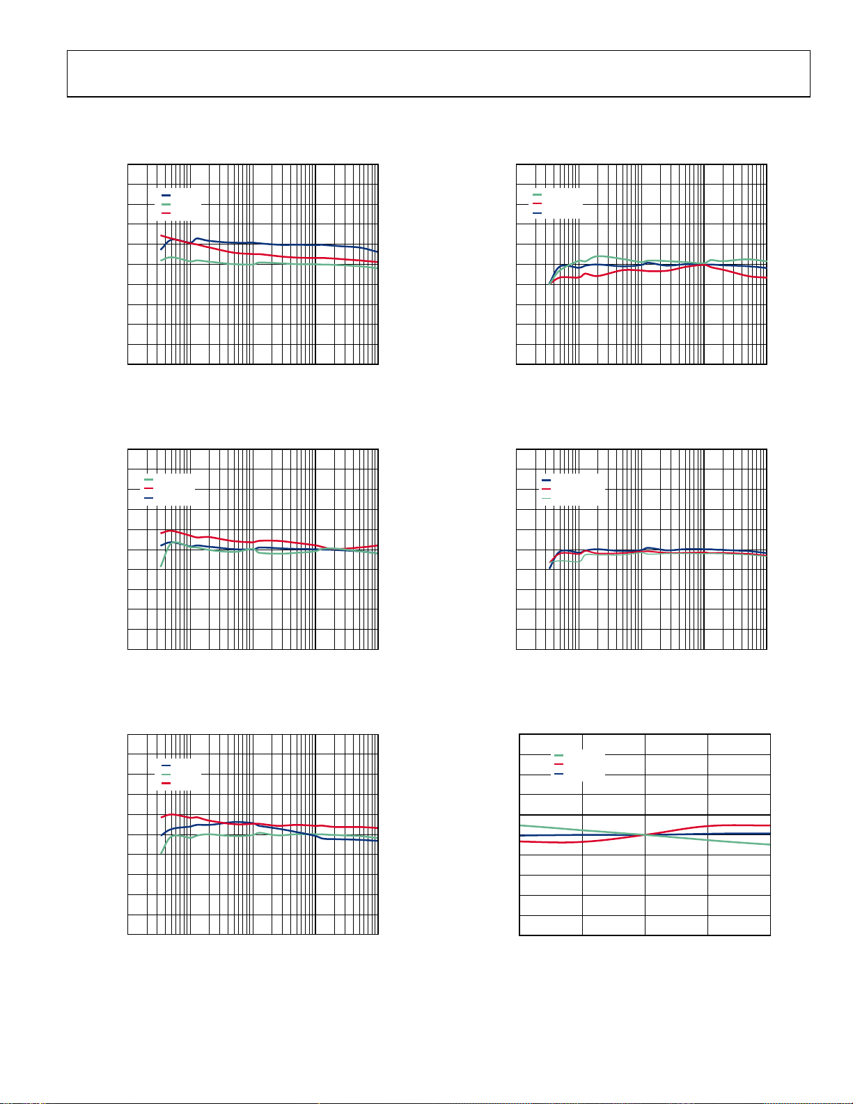
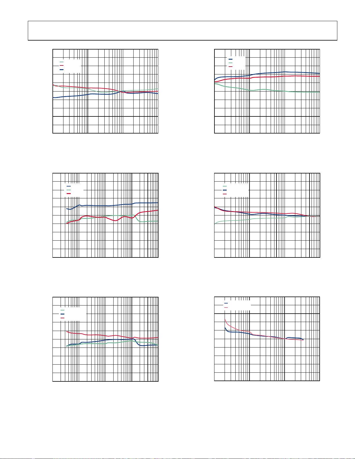
TYPICAL PERFORMANCE CHARACTERISTICS
1.0
0.8
0.6
0.4
0.2
0
–0.2
–0.4
ERROR (% OF READI NG)
–0.6
–0.8
–1.0
0.01 0. 1 1 10 100
–40°C
+25°C
+85°C
CURRENT CHANNE L (% FULL SCALE)
09320-101
Figure 5. Current Channel A Active Energy Error as a Percentage of Reading
(Gain = 1, Power Factor = 1) over Temperature with Internal Reference,
Integrator Off
1.0
0.8
0.6
0.4
0.2
–0.2
–0.4
ERROR (% OF READI NG)
–0.6
–0.8
–1.0
PF = –0.5
PF = +0.5
PF = +1.0
0
0.01 0. 1
CURRENT CHANNE L (% FULL SCALE)
1
10 100
09320-102
Figure 6. Current Channel A Active Energy Error as a Percentage of Reading
(Gain = 1, Temperature = 25°C) over Power Factor with Internal Reference,
Integrator Off
1.0
0.8
0.6
0.4
0.2
0
–0.2
–0.4
ERROR (% OF READI NG)
–0.6
–0.8
–1.0
0.01 0. 1
–40°C
+25°C
+85°C
CURRENT CHANNE L (% FULL SCALE)
1
10 100
09320-103
Figure 7. Current Channel A Active Energy Error as a Percentage of Reading
(Gain = 22, Power Factor = 1) over Temperature with Internal Reference,
Integrator Off
1.0
0.8
0.6
0.4
0.2
–0.2
–0.4
ERROR (% OF READI NG)
–0.6
–0.8
–1.0
PF = –0.5
PF = +0.5
PF = +1.0
0
0.01 0. 1
CURRENT CHANNE L (% FULL SCALE)
1
10 100
09320-104
Figure 8. Current Channel A Active Energy Error as a Percentage of Reading
(Gain = 22, Temperature = 25°C) over Power Factor with Internal Reference,
Integrator Off
1.0
0.8
0.6
0.4
0.2
0
–0.2
–0.4
ERROR (% OF READI NG)
–0.6
–0.8
–1.0
0.01 0. 1
VDD = 3.30V
VDD = 2.97V
VDD = 3.63V
CURRENT CHANNE L (% FULL SCALE)
1
10 100
09320-105
Figure 9. Current Channel A Active Energy Error as a Percentage of Reading
(Gain = 22, Temperature = 25°C, Power Factor = 1) over Supply Voltage
with Internal Reference, Integrator Off
1.0
0.8
0.6
0.4
0.2
0
–0.2
–0.4
ERROR (% OF READING)
–0.6
–0.8
– 1.0
45 50 55
PF = –0.5
PF = +0.5
PF = +1.0
FREQUENC Y (Hz)
60 65
09320-106
Figure 10. Current Channel A Active Energy Error as a Percentage of Reading
(Gain = 22, Temperature = 25°C) over Frequency and Power Factor
with Internal Reference, Integrator Off
Rev. A | Page 11 of 68
Page 12
ADE7953 Data Sheet
1.0
0.8
0.6
0.4
0.2
0
–0.2
–0.4
ERROR (% OF READI NG)
–0.6
–0.8
–1.0
0.01 0. 1
–40°C
+25°C
+85°C
CURRENT CHANNE L (% FULL SCALE)
1
10 100
09320-107
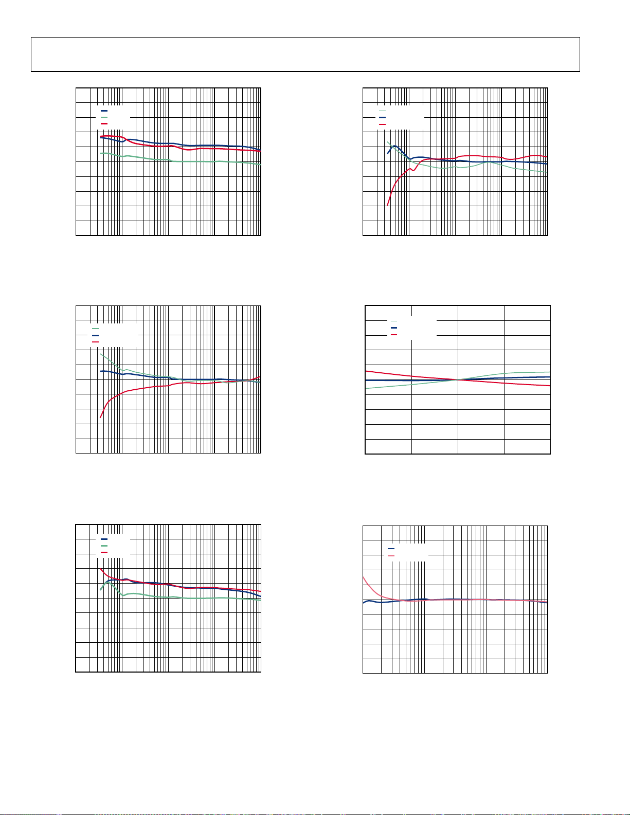
Figure 11. Current Channel A Reactive Energy Error as a Percentage of Reading
(Gain = 1, Power Factor = 0) over Temperature with Internal Reference,
Integrator Off
1.0
0.8
0.6
0.4
0.2
0
–0.2
–0.4
ERROR (% OF READI NG)
–0.6
–0.8
–1.0
0.01 0. 1
PF = –0.866
PF = 0
PF = +0.866
CURRENT CHANNE L (% FULL SCALE)
1
10 100
09320-110
Figure 14. Current Channel A Reactive Energy Error as a Percentage of Reading
(Gain = 22, Temperature = 25°C) over Power Factor with Internal Reference,
Integrator Off
1.0
0.8
0.6
0.4
0.2
0
–0.2
–0.4
ERROR (% OF READI NG)
–0.6
–0.8
–1.0
0.01 0. 1
PF = –0.866
PF = 0
PF = +0.866
CURRENT CHANNE L (% FULL SCALE)
1
10 100
09320-108
Figure 12. Current Channel A Reactive Energy Error as a Percentage of Reading
(Gain = 1, Temperature = 25°C) over Power Factor with Internal Reference,
Integrator Off
1.0
0.8
0.6
0.4
0.2
0
–0.2
–0.4
ERROR (% O F READI NG)
–0.6
–0.8
–1.0
0.01 0. 1 1 10 100
–40°C
+25°C
+85°C
CURRENT CHANNE L (% FULL SCALE)
09320-109
Figure 13. Current Channel A Reactive Energy Error as a Percentage of Reading
(Gain = 22, Power Factor = 0) over Temperature with Internal Reference,
Integrator Off
1.0
0.8
0.6
0.4
0.2
0
–0.2
–0.4
ERROR (% OF READING)
–0.6
–0.8
– 1.0
45 50 55
PF = –0.866
PF = 0
PF = +0.866
FREQUENC Y (Hz)
60 65
09320-111
Figure 15. Current Channel A Reactive Energy Error as a Percentage of Reading
(Gain = 22, Temperature = 25°C) over Frequency and Power Factor
with Internal Reference, Integrator Off
1.0
0.8
0.6
0.4
0.2
0
–0.2
–0.4
ERROR (% OF READI NG)
–0.6
–0.8
–1.0
0.1 1 10 100
GAIN = 1
GAIN = 22
CURRENT CHANNE L (% FULL SCALE)
09320-112
Figure 16. Current Channel A IRMS Error as a Percentage of Reading
(Temperature = 25°C, Power Factor = 1) over Gain with Internal Reference,
Integrator Off
Rev. A | Page 12 of 68
Page 13
Data Sheet ADE7953
1.0
0.8
0.6
0.4
0.2
0
–0.2
–0.4
ERROR (% OF READI NG)
–0.6
–0.8
–1.0
0.1
–40°C
+25°C
+85°C
1
CURRENT CHANNE L (% FULL SCALE)
10 100
09320-113
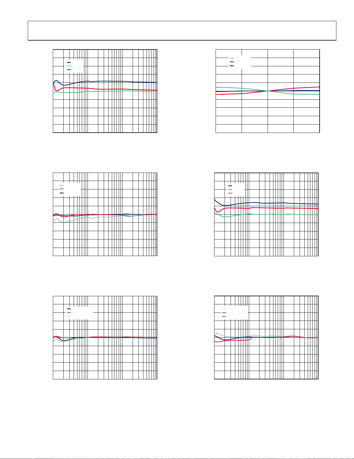
Figure 17. Current Channel B Active Energy Error as a Percentage of Reading
(Gain = 1, Power Factor = 1) over Temperature with Internal Reference,
Integrator Off
1.0
0.8
0.6
0.4
0.2
0
–0.2
–0.4
ERROR (% OF READI NG)
–0.6
–0.8
– 1.0
45 50 55
PF = –0.5
PF = +0.5
PF = +1.0
FREQUENCY (Hz)
60 65
09320-116
Figure 20. Current Channel B Active Energy Error as a Percentage of Reading
(Gain = 1, Temperature = 25°C) over Frequency and Power Factor
with Internal Reference, Integrator Off
1.0
0.8
0.6
0.4
0.2
–0.2
–0.4
ERROR (% OF READI NG)
–0.6
–0.8
–1.0
PF = –0.5
PF = +0.5
PF = +1.0
0
0.1
1
CURRENT CHANNE L (% FULL SCALE)
10 100
09320-114
Figure 18. Current Channel B Active Energy Error as a Percentage of Reading
(Gain = 1, Temperature = 25°C) over Power Factor with Internal Reference,
Integrator Off
1.0
0.8
0.6
0.4
0.2
0
–0.2
–0.4
ERROR (% OF READI NG)
–0.6
–0.8
–1.0
0.1
VDD = 3.30V
VDD = 2.97V
VDD = 3.63V
1
CURRENT CHANNE L (% FULL SCALE)
10 100
09320-115
Figure 19. Current Channel B Active Energy Error as a Percentage of Reading
(Gain = 1, Temperature = 25°C, Power Factor = 1) over Supply Voltage
with Internal Reference, Integrator Off
1.0
0.8
0.6
0.4
0.2
0
–0.2
–0.4
ERROR (% OF READI NG)
–0.6
–0.8
–1.0
0.1 1 10 100
–40°C
+25°C
+85°C
CURRENT CHANNE L (% FULL SCALE)
09320-117
Figure 21. Current Channel B Reactive Energy Error as a Percentage of Reading
(Gain = 1, Power Factor = 0) over Temperature with Internal Reference,
Integrator Off
1.0
0.8
0.6
0.4
0.2
–0.2
–0.4
ERROR (% OF READI NG)
–0.6
–0.8
–1.0
PF = –0.866
PF = 0
PF = +0.866
0
0.1 1 10 100
CURRENT CHANNE L (% FULL SCALE)
09320-118
Figure 22. Current Channel B Reactive Energy Error as a Percentage of Reading
(Gain = 1, Temperature = 25°C) over Power Factor with Internal Reference,
Integrator Off
Rev. A | Page 13 of 68
Page 14
ADE7953 Data Sheet
1.0
0.8
0.6
0.4
0.2
0
–0.2
–0.4
ERROR (% OF READING)
–0.6
–0.8
– 1.0
45 50 55
PF = –0.866
PF = 0
PF = +0.866
FREQUENC Y (Hz)
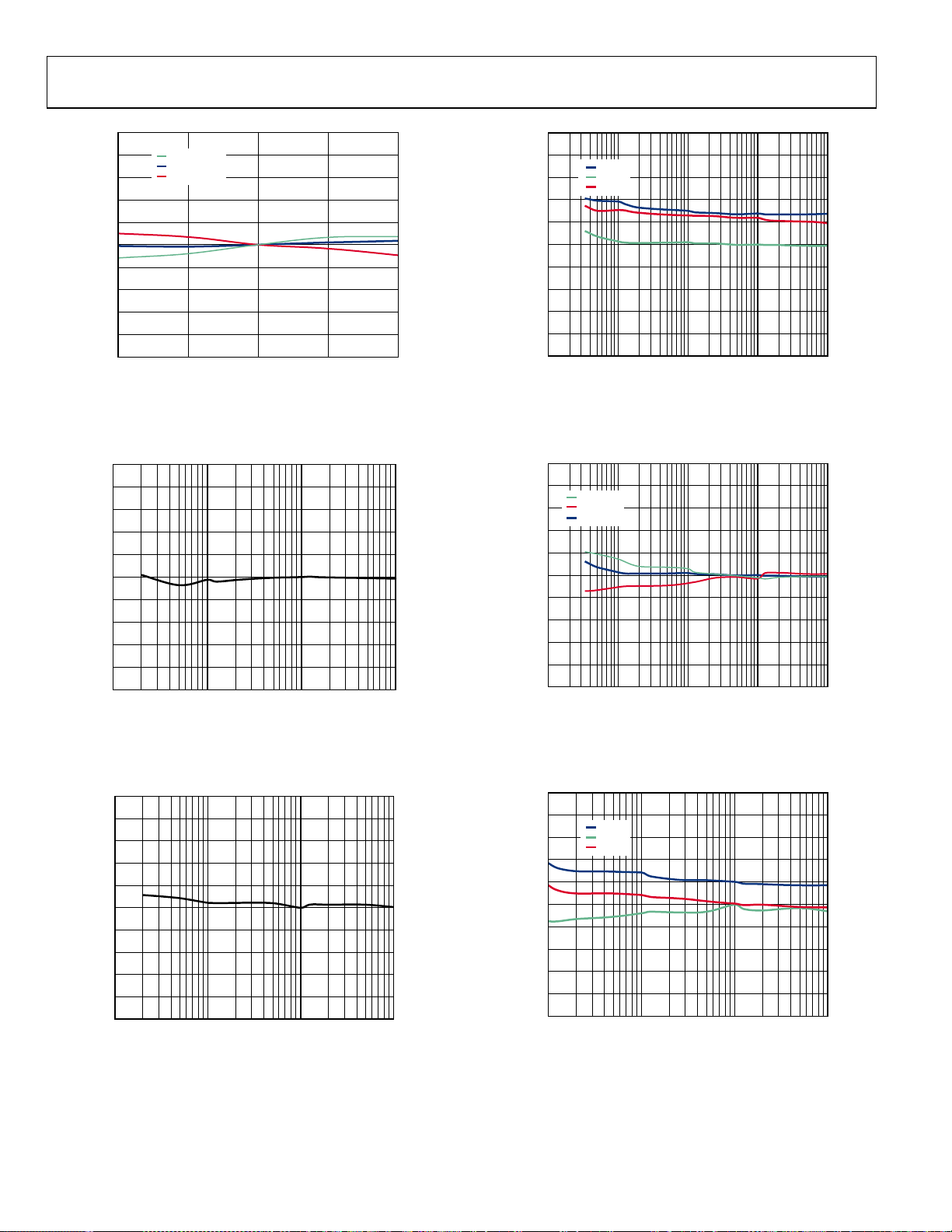
60
09320-219
65
Figure 23. Current Channel B Reactive Energy Error as a Percentage of Reading
(Gain = 1, Temperature = 25°C) over Frequency and Power Factor
with Internal Reference, Integrator Off
1.0
0.8
0.6
0.4
0.2
0
–0.2
–0.4
ERROR (% OF READING )
–0.6
–0.8
–1.0
0.01 0. 1 1 10 100
–40°C
+25°C
+85°C
CURRENT CHANNE L (% FULL SCALE)
09320-122
Figure 26. Current Channel A Active Energy Error as a Percentage of Reading
(Gain = 16, Power Factor = 1) over Temperature with Internal Reference,
Integrator On
1.0
0.8
0.6
0.4
0.2
0
–0.2
–0.4
ERROR (% O F READI NG)
–0.6
–0.8
–1.0
0.1 1 10 100
CURRENT CHANNE L (% FULL SCALE)
Figure 24. Current Channel B IRMS Error as a Percentage of Reading
(Gain = 1, Temperature = 25°C, Power Factor = 1)
with Internal Reference, Integrator Off
1.0
0.8
0.6
0.4
0.2
0
–0.2
–0.4
ERROR (% OF READING)
–0.6
–0.8
0.1 1 10 100
VOLTAG E CHANNEL (% FULL SCALE)
Figure 25. VRMS Error as a Percentage of Reading (Temperature = 25°C,
Power Factor = 1) with Internal Reference, Integrator Off
1.0
0.8
0.6
0.4
0.2
–0.2
–0.4
ERROR (% OF READING )
–0.6
–0.8
–1.0
09320-220
Figure 27. Current Channel A Active Energy Error as a Percentage of Reading
PF = –0.5
PF = +0.5
PF = +1.0
0
0.01 0. 1
CURRENT CHANNE L (% FULL SCALE)
1
10 100
09320-123
(Gain = 16, Temperature = 25°C) over Power Factor with Internal Reference,
Integrator On
1.0
0.8
0.6
0.4
0.2
0
–0.2
–0.4
ERROR (% OF READING )
–0.6
–0.8
–1.0
0.1
09320-121
–40°C
+25°C
+85°C
1
CURRENT CHANNE L (% FULL SCALE)
10 100
09320-124
Figure 28. Current Channel B Active Energy Error as a Percentage of Reading
(Gain = 16, Power Factor = 1) over Temperature with Internal Reference,
Integrator On
Rev. A | Page 14 of 68
Page 15
Data Sheet ADE7953
1.0
0.8
0.6
0.4
0.2
–0.2
–0.4
ERROR (% OF READING )
–0.6
–0.8
–1.0
PF = –0.5
PF = +0.5
PF = +1.0
0
0.1 1 10 100
CURRENT CHANNEL (% F ULL SCALE)
09320-225
Figure 29. Current Channel B Active Energy Error as a Percentage of Reading
(Gain = 16, Temperature = 25°C) over Power Factor with Internal Reference,
Integrator On
1.0
0.8
0.6
0.4
0.2
0
–0.2
–0.4
ERROR (% OF READING )
–0.6
–0.8
–1.0
0.1 1 10 100
–40°C
+25°C
+85°C
CURRENT CHANNEL (% F ULL SCALE)
09320-228
Figure 32. Current Channel B Reactive Energy Error as a Percentage of Reading
(Gain = 16, Power Factor = 0) over Temperature with Internal Reference,
Integrator On
1.0
0.8
0.6
0.4
0.2
0
–0.2
–0.4
ERROR (% OF READI NG)
–0.6
–0.8
–1.0
0.01 0.1 1 10 100
–40°C
+25°C
+85°C
CURRENT CHANNE L (% FULL SCALE)
09320-126
Figure 30. Current Channel A Reactive Energy Error as a Percentage of Reading
(Gain = 16, Power Factor = 0) over Temperature with Internal Reference,
Integrator On
1.0
0.8
0.6
0.4
0.2
–0.2
–0.4
ERROR (% OF READI NG)
–0.6
–0.8
–1.0
PF = –0.866
PF = 0
PF = +0.866
0
0.01 0.1 1 10 100
CURRENT CHANNE L (% FULL SCALE)
09320-227
Figure 31. Current Channel A Reactive Energy Error as a Percentage of Reading
(Gain = 16, Temperature = 25°C) over Power Factor with Internal Reference,
Integrator On
1.0
0.8
0.6
0.4
0.2
–0.2
–0.4
ERROR (% OF READI NG)
–0.6
–0.8
–1.0
PF = –0.866
PF = 0
PF = +0.866
0
0.1 1 10 100
CURRENT CHANNE L (% FULL SCALE)
09320-129
Figure 33. Current Channel B Reactive Energy Error as a Percentage of Reading
(Gain = 16, Temperature = 25°C) over Power Factor with Internal Reference,
Integrator On
1.0
0.8
0.6
0.4
0.2
0
–0.2
–0.4
ERROR (% O F READI NG)
–0.6
–0.8
–1.0
CHANNEL A
CHANNEL B
0.1 1 10 100
CURRENT CHANNE L (% FULL SCALE)
09320-130
Figure 34. IRMS Error as a Percentage of Reading (Gain = 16,
Temperature = 25°C) with Internal Reference, Integrator On
Rev. A | Page 15 of 68
Page 16
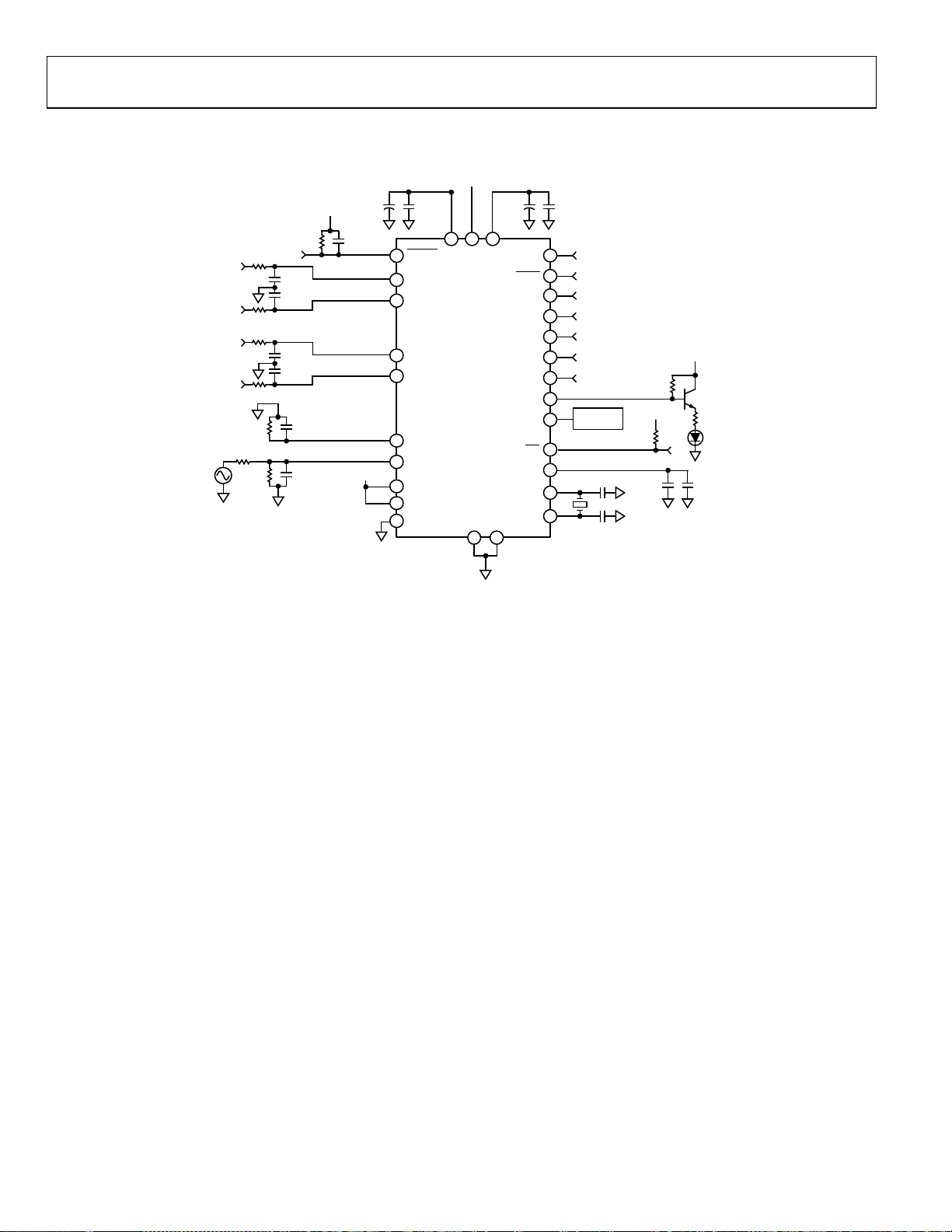
ADE7953 Data Sheet
V
TEST CIRCUIT
3.3
+ +
110V
1MΩ
1kΩ
1kΩ
1kΩ
1kΩ
1kΩ
1kΩ
33nF
33nF
33nF
33nF
10kΩ
33nF
33nF
3.3V
1µF
4.7µF
3.3V
0.1µF
RESET
2
IAP
5
6
IAN
9
IBP
10
IBN
11
VN
12
VP
7
PULL_HIGH
8
PULL_HIGH
14
PULL_LOW
17
15
VDD
VINTA
MOSI/SCL/Rx
MISO/ SDA/Tx
ADE7953
DGND
416
4.7µF
3
VINTD
CLKOUT
AGND
ZX
REVP
ZX_I
CS
SCLK
CF2
CF1
IRQ
REF
CLKIN
0.1µF
1
20
21
28
27
10kΩ
3.3V
3.3V
500Ω
+
0.1µF
26
25
24
SAME AS
23
CF2
20pF
3.58MHz
20pF
10kΩ
4.7µF
22
13
19
18
09320-099
Figure 35. Test Circuit
Rev. A | Page 16 of 68
Page 17

Data Sheet ADE7953
r
t
TERMINOLOGY
Measurement Error ADC Offset Error
The error associated with the energy measurement made by the
ADE7953 is defined by
Measuremen (1)
Phase Error Between Channels
The high-pass filter (HPF) and digital integrator introduce a
slight phase mismatch between the current channels and the
voltage channel. The all-digital design ensures that the phase
matching between the current channels and the voltage channel
is within ±0.05° over a range of 45 Hz to 65 Hz. This internal
phase mismatch can be combined with the external phase error
(from current sensor or component tolerance) and calibrated
with the phase calibration registers.
Power Supply Rejection (PSR)
PSR quantifies the ADE7953 measurement error as a percentage
of reading when the power supplies are varied. For the ac PSR
measurement, a reading at nominal supplies (3.3 V) is taken. A
second reading is obtained with the same input signal levels when
an ac signal (120 mV rms/100 Hz) is introduced onto the supplies.
Any error introduced by this ac signal is expressed as a percentage
of reading (see the Measurement Error definition). For the dc PSR
measurement, a reading at nominal supplies (3.3 V) is taken. A
second reading is obtained with the same input signal levels when
the power supplies are varied by ±10%. Any error introduced is
again expressed as a percentage of reading.
= Erro
−
EnergyTrue ADE7953 by Registered Energy
EnergyTrue
%100×
The ADC offset error refers to the dc offset associated with the
analog inputs to the ADCs. It means that, with the analog inputs
connected to AGND, the ADCs still see a dc analog input signal.
The magnitude of the offset depends on the gain and input range
selection. However, the offset is removed from the current and
voltage channels by a high-pass filter (HPF), and the power
calculation is not affected by this offset.
Gain Error
The gain error in the ADCs of the ADE7953 is defined as the
per-channel difference between the measured ADC output code
(minus the offset) and the ideal output code (see the Current
Channel ADCS section and the Voltage Channel ADC section).
The difference is expressed as a percentage of the ideal code.
Rev. A | Page 17 of 68
Page 18

ADE7953 Data Sheet
ADE7953 POWER-UP PROCEDURE
The ADE7953 contains an on-chip power supply monitor that
supervises the power supply (VDD). While the voltage applied
to the VDD pin is below 2 V ± 10%, the chip is in an inactive
state. Once VDD crosses the 2 V ± 10% threshold, the power
supply monitor keeps the ADE7953 in an inactive state for an
additional 26 ms. This time delay allows VDD to reach the
minimum specified operating voltage of 3.3 V – 10%. Once
the minimum specified operating voltage is met, the internal
circuitry is enabled; this is accomplished in approximately
40 ms.
Once the start-up sequence is complete and the ADE7953 is
ready to receive communication from a microcontroller, the
reset flag is set in the IRQSTATA register (Address 0x22D and
Address 0x32D). An external interrupt is triggered on the IRQ
pin. The reset interrupt is enabled by default and cannot be
disabled, hence an external interrupt always occurs at the end
of a power-up procedure, hardware or software reset.
It is highly recommended that the reset interrupt is used by the
microcontroller to gate the first communication with the
ADE7953. If the interrupt is not used, a timeout can be
implemented; however, as the start-up sequence can vary partto-part and over temperature, a timeout of a least 100 ms is
recommended. The reset interrupt provides the most efficient
way of monitoring the completion of the ADE7953 start-up
sequence.
Once the start-up sequence is complete, communication with
the ADE7953 can begin. See the Communicating with the
ADE7953 section for further details.
REQUIRED REGISTER SETTING
For optimum performance, Register Address 0x120 must be
configured by the user after powering up the ADE7953. This
register ensures that the optimum timing configuration is
selected to maximize the accuracy and dynamic range. This
register is not set by default and thus must be written by the
user each time the ADE7953 is powered up. Register 0x120 is
a protected register and thus a key must be written to allow the
register to be modified. The following sequence should be
followed:
• Write 0xAD to Register Address 0xFE: This unlocks
the register 0x120
•
Write 0x30 to Register Address 0x120: This configures the
optimum settings
The above two instructions must be performed in succession to
be successful.
Rev. A | Page 18 of 68
Page 19
Data Sheet ADE7953
R
THEORY OF OPERATION
ANALOG INPUTS
The ADE7953 includes three analog inputs that form two current
channels and one voltage channel. In a standard configuration,
Current Channel A is used to measure the phase current, and
Current Channel B is used to measure the neutral current. The
voltage channel input measures the difference between the phase
voltage and the neutral voltage. The ADE7953 can, however, be
used with alternative voltage and current combinations as long as
the analog input specifications described in this section are met.
Current Channel A
Current Channel A is a fully differential voltage input that is
designed to be used with a current sensor. This input is driven
by two pins: IAP (Pin 5) and IAN (Pin 6). The maximum differential voltage that can be applied to IAP and IAN is ±500 mV.
A common-mode voltage of less than ±25 mV is recommended.
Common-mode voltages in excess of this recommended value
may limit the available dynamic range. A programmable gain
amplifier (PGA) stage is provided on Current Channel A with
gain options of 1, 2, 4, 8, 16, and 22 (see Tab l e 6 ).
The maximum full-scale input of Current Channel A is ±250 mV
when using a single-ended configuration and, therefore, when
using a gain setting of 1, the dynamic range is limited. The Current
Channel A gain is configured by writing to the PGA_IA register
(Address 0x008). By default, the Current Channel A PGA is set
to 1. A gain option of 22 is offered exclusively on Current
Channel A, allowing high accuracy measurement for signals of
very small amplitude. This configuration is particularly useful
when using small value shunt resistors or Rogowski coils.
Current Channel B
Current Channel B is a fully differential voltage input that is
designed to be used with a current sensor. This input is driven
by two pins: IBP (Pin 9) and IBN (Pin 10). The maximum differential voltage that can be applied to IBP and IBN is ±500 mV. A
common-mode voltage of less than ±25 mV is recommended.
Common-mode voltages in excess of this recommended value
may limit the available dynamic range. A PGA gain stage is
provided on Current Channel B with gain options of 1, 2, 4, 8,
and 16 (see Tabl e 6 ). The Current Channel B gain is configured
by writing to the PGA_IB register (Address 0x009). By default,
the Current Channel B PGA is set to 1.
Voltage Channel
The voltage channel input a full differential input driven by
two pins: VP (Pin 12) and VN (Pin 11). The voltage channel
is typically connected in a single-ended configuration. The
maximum single-ended voltage that can be applied to VP is
±500 mV with respect to VN. A common-mode voltage of less
than ±25 mV is recommended. Common-mode voltages in
excess of this recommended value may limit the dynamic range
capabilities of the ADE7953. A PGA gain stage is provided on
the voltage channel with gain options of 1, 2, 4, 8, and 16 (see
Tabl e 6 ).
The voltage channel gain is configured by writing to the PGA_V
register (Address 0x007). By default, the voltage channel PGA is
set to 1.
Table 6. PGA Gain Settings
Full-Scale
Gain
1
Differential
Input (mV)
1 ±500 0001 000 000
2 ±250 001 001 001
4 ±125 010 010
8 ±62.5 011 011
16 ±31.25 100 100
22 ±22.7 101 N/A N/A
When a gain of 1 is selected on Current Channel A, the maximum pin input is
limited to ±250 mV. Therefore, when using a single-ended configuration, the
maximum input is ±250 mV with respect to AGND.
PGA_IA[2:0]
(Addr 0x008)
PGA_IB[2:0]
(Addr 0x009)
PGA_V[2:0]
(Addr 0x007)
010
011
100
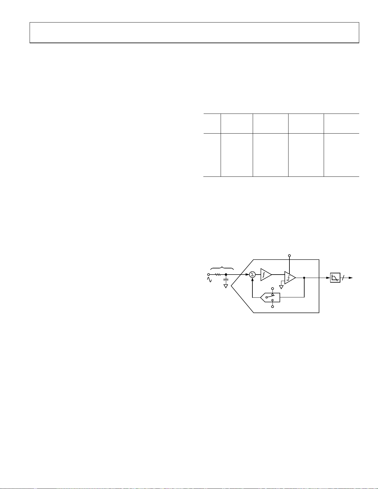
ANALOG-TO-DIGITAL CONVERSION
The analog-to-digital conversion in the ADE7953 is performed
by three second-order Σ- modulators. For the sake of clarity,
the block diagram in Figure 36 shows the operation of a firstorder Σ- modulator. The analog-to-digital conversion consists
of a Σ- modulator followed by a low-pass filter stage.
CLKIN/4
ANALOG
LOW-PASS FILTE
R
C
INTEGRATOR
+
–
Figure 36. Σ-Δ Conversion
+V
REF
–V
REF
+
–
.....10100101... ..
1-BIT DAC
LATCHED
COMPARATOR
The Σ- modulator converts the input signal into a continuous
serial stream of 1s and 0s at a rate determined by the sampling
clock. The ADE7953 sampling clock is equal to 895 kHz
(CLKIN/4). The 1-bit DAC in the feedback loop is driven by the
serial data stream. The DAC output is subtracted from the input
signal. If the loop gain is high enough, the average value of the
DAC output (and, therefore, the bit stream) can approach that
of the input signal level. For any given input value in a single
sampling interval, the data from the 1-bit ADC is virtually
meaningless. A meaningful result is obtained only when a large
number of samples is averaged. This averaging is carried out
in the second part of the ADC, the digital low-pass filter. By
averaging a large number of bits from the modulator, the lowpass filter can produce 24-bit data-words that are proportional
to the input signal level. The
Σ-∆ converter uses two techniques—
oversampling and noise shaping—to achieve high resolution
from what is essentially a 1-bit conversion technique.
DIGITAL
LOW-PASS
FILTER
24
09320-013
Rev. A | Page 19 of 68
Page 20
ADE7953 Data Sheet
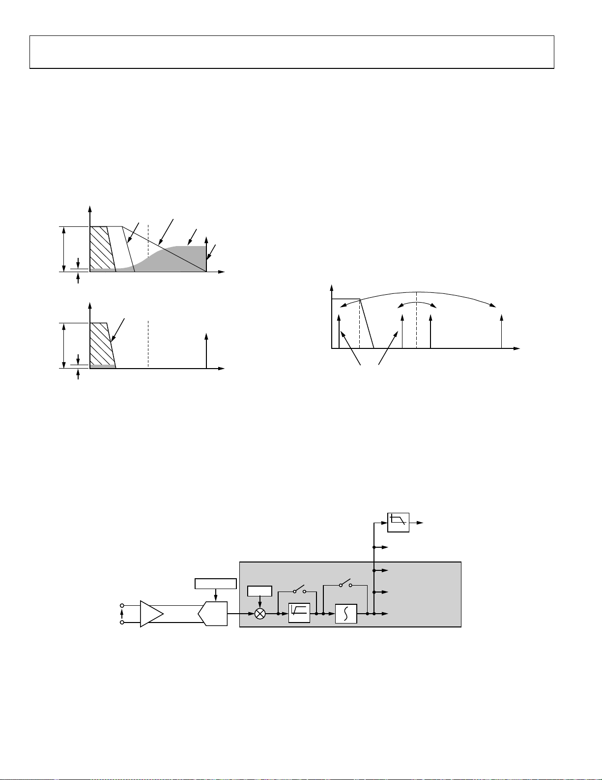
A
Oversampling
Oversampling is the first technique used to achieve high
resolution. Oversampling means that the signal is sampled at a
rate (frequency) that is many times higher than the bandwidth
of interest. For example, the sampling rate in the ADE7953 is
895 kHz, and the bandwidth of interest is 40 Hz to 1.23 kHz.
Oversampling has the effect of spreading the quantization noise
(noise due to sampling) over a wider bandwidth. With the noise
spread more thinly over a wider bandwidth, the quantization
noise in the band of interest is lowered (see Figure 37).
ANTIALIASI NG FILTER
SIGNAL
SIGNAL
NOISE
0 3 447. 5
DIGITAL FILTER
FREQUENCY (kHz)
HIGH RESOLUTION
OUTPUT FROM
DIGITAL LPF
(RC)
SHAPED NOISE
895
SAMPLING
FREQUENCY
Noise Shaping
Noise shaping is the second technique used to achieve high
resolution. In the
Σ-∆ modulator, the noise is shaped by the
integrator, which has a high-pass-type response for the quantization noise due to feedback. The result is that most of the noise
is at the higher frequencies, where it can be removed by the
digital low-pass filter. This noise shaping is shown in Figure 37.
Antialiasing Filter
As shown in Figure 36, an external low-pass RC filter is required
on the input to each modulator. The role of this filter is to prevent
aliasing. Aliasing refers to the frequency components in the input
signal that are folded back and appear in the sampled signal. This
effect occurs with signals that are higher than half the sampling
rate of the ADC (also known as the Nyquist frequency) appearing in the sampled signal at a frequency below half the sampling
rate. This concept is depicted in Figure 38.
LIASING E FFECTS
SAMPLING
FREQUENCY
NOISE
0 3 447. 5
FREQUENCY (kHz)
895
09320-014
Figure 37. Noise Reduction due to Oversampling and
Noise Shaping in the Analog Modulator
However, oversampling alone is not sufficient to improve the
signal-to-noise ratio (SNR) in the bandwidth of interest. For
example, an oversampling ratio of 4 is required to increase the
SNR by only 6 dB (1 bit). To keep the oversampling ratio at a
reasonable level, it is possible to shape the quantization noise so
that the majority of the noise lies at the higher frequencies (see
the following section.
DSP
IxP
V
IN
IxN
PGA_x BITS
×1, ×2, ×4, ×8, ×16,
×22 (FOR IA ONLY)
PGA
REFERENCE
ADC
xIGAIN
Figure 39. Current Channel ADC and Signal Path
0 1.23 3 447.5
IMAGE
FREQUENCIES
FREQUENCY (kHz)
Figure 38. Aliasing Effect
The arrows shown in Figure 38 depict the frequency components above the Nyquist frequency (447.5 kHz in the case of
the ADE7953) being folded back down. Aliasing occurs with
all ADCs, regardless of the architecture.
ZX_I DETECTION
9320-019
HPFEN BIT
CONFIG[2]
HPF
INTENx BIT
CONFI G[1:0]
DIGITAL
INTEGRATOR
LPF1
CURRENT PEAK,
OVERCURRENT
DETECTIO N
CURRENT RMS (IRMS)
CALCULATION
Ix WAVEFORM
SAMPLING REGISTER
ACTIVE AND REACTIVE
POWER CALCUL ATION
895
09320-015
Rev. A | Page 20 of 68
Page 21

Data Sheet ADE7953
CURRENT CHANNEL ADCs
Figure 39 shows the ADC signal path and signal processing for
Current Channel A, which is accessed through the IAP and IAN
pins. The signal path for Current Channel B is identical and is
accessed through the IBP and IBN pins. The ADC output is a
twos complement, 24-bit data-word that is available at a rate of
6.99 kSPS (thousand samples per second). With the specified fullscale analog input of ±250 mV and a PGA_Ix gain setting of 2,
the ADC produces its maximum output code. The ADC output
swings between −6,500,000 LSBs (decimal) and +6,500,000 LSBs.
This output varies from part to part.
As shown in Figure 39, there is a high-pass filter (HPF) in each
current channel signal path. The HPF is enabled by default and
removes any dc offset in the ADC output. It is highly recommended that this filter be enabled at all times, but it can be
disabled by clearing the HPFEN bit (Bit 2) in the CONFIG
register (Address 0x102). Clearing the HPFEN bit disables the
filters in both current channels and in the voltage channel.
di/dt Current Sensor and Digital Integrator
As shown in Figure 39, the current channel signal path for both
Channel A and Channel B includes an internal digital integrator.
This integrator is disabled by default and is required only when
interfacing with a di/dt sensor, such as a Rogowski coil. When
using either a shunt resistor or a current transformer (CT), this
integrator is not required and should remain disabled.
A di/dt sensor detects changes in the magnetic field caused by
ac current. Figure 40 shows the principle of a di/dt current sensor.
MAGNETIC F IELD CREATED BY CURRENT
(DIRECTLY PROPORT IONAL TO CURRENT)
+ EMF (ELECTROMOTIVE FORCE)
– INDUCED BY CHANGES IN
MAGNETIC FLUX DENSITY (di/dt)
Figure 40. Principle of a di/dt Current Sensor
09320-020
The flux density of a magnetic field induced by a current is
directly proportional to the magnitude of the current. Changes
in the magnetic flux density passing through a conductor loop
generate an electromotive force (EMF) between the two ends of
the loop. The EMF is a voltage signal that is proportional to the
differential of the current over time (di/dt). The voltage output
from the di/dt sensor is determined by the mutual inductance
between the current-carrying conductor and the di/dt sensor.
The current signal must be recovered from the di/dt signal
before it can be used. An integrator is therefore necessary to
restore the signal to its original form.
The ADE7953 has a built-in digital integrator on each current
channel that recovers the current signal from the di/dt sensor.
Both digital integrators are disabled by default. The digital
integrator on Current Channel A is enabled by setting the
INTENA bit (Bit 0) in the CONFIG register (Address 0x102).
The digital integrator on Current Channel B is enabled by setting
the INTENB bit (Bit 1) in the CONFIG register (Address 0x102).
VOLTAGE CHANNEL ADC
Figure 41 shows the ADC signal path and signal processing for
the voltage channel input, which is accessed through the VP and
VN pins. The ADC output is a twos complement, 24-bit dataword that is available at a rate of 6.99 kSPS (thousand samples
per second). With the specified full-scale analog input of ±500 mV
and a PGA_V gain setting of 1, the ADC produces its maximum
output code. The ADC output swings between −6,500,000 LSBs
(decimal) and +6,500,000 LSBs. Note that this output varies
from part to part.
As shown in Figure 41, there is a high-pass filter (HPF) in the
voltage channel signal path. The HPF is enabled by default and
removes any dc offset in the ADC output. It is highly recommended that this filter be enabled at all times, but it can be
disabled by clearing the HPFEN bit (Bit 2) in the CONFIG
register (Address 0x102). Clearing the HPFEN bit disables the
filters in both current channels and in the voltage channel.
Rev. A | Page 21 of 68
Page 22

ADE7953 Data Sheet
V
REFERENCE CIRCUIT
The ADE7953 has an internal voltage reference of 1.2 V nominal,
which appears on the REF pin. This reference voltage is used by
the ADCs in the ADE7953. The REF pin can be overdriven by
an external source, for example an external 1.2 V reference. The
voltage of the ADE7953 internal reference drifts slightly over
temperature (see the Specifications section). The value of the temperature drift may vary slightly from part to part. A drift of x% in
PGA_V BITS
×1, ×2, ×4, ×8, ×16
VP
V
IN
PGA
VN
REFERENCE
ADC
Figure 41. Voltage Channel ADC and Signal Path
DSP
VGAIN
the reference results in a 2x% deviation in meter accuracy. The
reference drift is typically minimal and is usually much smaller
than the drift of other components in the meter. By default, the
ADE7953 is configured to use the internal reference. If Bit 0 of
the EX_REF register (Address 0x800) is set to 1, an external
voltage reference can be applied to the REF pin.
OLTAGE PEAK,
OVERVOLTAGE,
SAG DETECTI ON
VOLTAGE RMS (VRMS)
HPFEN BIT
CONFIG[2]
HPF
CALCUL ATION
VWAVEFORM
SAMPLING REGIST ER
ACTIVE AND REACTIVE
POWER CALCULATION
LPF1
ZX DETECTION
09320-025
Rev. A | Page 22 of 68
Page 23

Data Sheet ADE7953
ROOT MEAN SQUARE MEASUREMENT
Root mean square (rms) is a measurement of the magnitude
of an ac signal. Specifically, the rms of an ac signal is equal to
the amount of dc required to produce an equivalent amount
of power in the load. The rms is expressed mathematically in
Equation 1.
t
1
2
=
RMS
∫
t
0
(1)
dttf
)(
For time-sampled signals, rms calculation involves squaring
the signal, taking the average, and obtaining the square root.
N
=
RMS
2
nf
][1 (2)
∑
N
n
=
1
As implied by Equation 2, the rms measurement contains
information from the fundamental and all harmonics over
a 1.23 kHz measurement bandwidth.
The ADE7953 provide rms measurements for Current
Channel A, Current Channel B, and the voltage channel
simultaneously. These measurements have a settling time of
approximately 200 ms and are updated at a rate of 6.99 kHz.
CURRENT CHANNEL RMS CALCULATION
The ADE7953 provides rms measurements for both Current
Channel A and Current Channel B. Figure 42 shows the signal
path for this calculation. The signal processing is identical for
Current Channel A and Current Channel B.
×IRMSOS[23:0]
12
2
CURRENT
SIGNAL
FROM HPF OR
INTEGRATOR
(IF ENABLED)
Figure 42. Current Channel RMS Signal Processing
As shown in Figure 42, the current channel ADC output samples
are used to continually compute the rms. The rms is achieved by
low-pass filtering the square of the output signal and then taking
a square root of the result. The 24-bit unsigned rms measurements
for Current Channel A and Current Channel B are available in
2
X
LPF
√
IRMSx[23:0]
09320-040
the IRMSA (Address 0x21A and Address 0x31A) and IRMSB
(Address 0x21B and Address 0x31B) registers, respectively. Both
of these registers are updated at a rate of 6.99 kHz. With fullscale inputs on Current Channel A and Current Channel B,
the expected reading on the IRMSA and IRMSB register is
9032007d.
Because the LPF used in the rms signal path is not ideal, it is
recommended that the IRMSx registers be read synchronously
to the zero-crossing signal (see the Zero-Crossing Detection
section). This helps to stabilize reading-to-reading variation
by removing the effect of any 2ω ripple present on the rms
measurement.
VOLTAGE CHANNEL RMS CALCULATION
The ADE7953 provides an rms measurement on the voltage
channel. Figure 43 shows the signal path for this calculation.
VRMSOS[23:0]
12
2
VOLTAG E
SIGNAL
FROM HPF
As shown in Figure 43, the voltage channel ADC output
samples are used to continually compute the rms. The rms is
achieved by low-pass filtering the square of the output signal
and then taking a square root of the result. The 24-bit unsigned
voltage channel rms measurement is available in the VRMS
register (Address 0x21C and Address 0x31C). This register is
updated at a rate of 6.99 kHz. With full-scale inputs on the
voltage channel, a VRMS reading of 9032007d can be expected.
Because the LPF used in the rms signal path is not ideal, it is
recommended that the VRMS register be read synchronously to
the zero-crossing signal (see the Zero-Crossing Detection section).
This helps to stabilize reading-to-reading variation by removing
the effect of any 2ω ripple present on the rms measurement.
2
X
Figure 43. Voltage Channel RMS Signal Processing
LPF
VRMS[23:0]
√
09320-041
Rev. A | Page 23 of 68
Page 24

ADE7953 Data Sheet
ACTIVE POWER CALCULATION
Power is defined as the rate of energy flow from the source to
the load. It is defined as the product of the voltage and current
waveforms. The resulting waveform is called the instantaneous
power signal and is equal to the rate of energy flow at every
instant of time. The unit of power is the watt or joules/sec.
(3)
)sin(2 ωt V V(t) ××=
(4)
)sin(2 ωt I I(t) ××=
where:
V is the rms voltage.
I is the rms current.
P(t) = V(t) × I(t) (5)
P(t) = VI − VI × cos(2ωt) (6)
The average power over an integral number of line cycles (n)
is given by the expression in Equation 7.
nT
1
P
nT
==
VIdttP
)(
∫
0
(7)
where:
P is the active or real power.
T is the line cycle period.
The active power is equal to the dc component of the instantaneous power signal (P(t) in Equation 5). The active power is
therefore equal to VI. This relationship is used to calculate active
power in the ADE7953. Figure 44 illustrates this concept.
VRMS
×
IRMS
INSTANTANEOUS
POWER SIGNAL
P(t) = VRMS × IRMS – VRMS × IRMS × cos(2ωt)
INSTANTANEOUS
ACTIVE POW ER SIGNAL:
VRMS × IRMS
The signal chain for the active power and energy calculations in
the ADE7953 is shown in Figure 45. The instantaneous power
signal P(t) is generated by multiplying the current and voltage
signals. The dc component of the instantaneous power signal
is then extracted by LPF2 (low-pass filter) to obtain the active
power information. Because LFP2 does not have an ideal “brick
wall” frequency response, the active power signal has some
ripple associated with it. This ripple is sinusoidal and has a
frequency equal to twice the line frequency. Because the ripple
is sinusoidal in nature, it is removed when the active power
signal is integrated to compute the active energy (see the Active
Energy Calculation section).
The ADE7953 computes the active power simultaneously on
Current Channel A and Current Channel B and stores the
resulting measurements in the AWATT (Address 0x212 and
Address 0x312) and BWATT (Address 0x213 and Address 0x313)
registers, respectively. With full-scale inputs, the expected
reading in the AWATT and BWATT registers is approximately
4862401 LSBs (decimal).
The active power measurements are taken over a bandwidth of
1.23 kHz and include the effects of any harmonics within that
range. The active power registers are updated at a rate of 6.99 kHz
and can be read using the waveform sampling mode (see the
Instantaneous Powers and Waveform Sampling section).
SIGN OF ACTIVE POWER CALCULATION
The active power measurement in the ADE7953 is a signed
calculation. If the phase differential between the current and
voltage waveforms is more than 90°, the power is negative.
Negative power indicates that energy is being injected back
into the grid. The ACCMODE register (Address 0x201 and
Address 0x301) includes two sign indication bits that show the
sign of the active power of Current Channel A (APSIGN_A)
and Current Channel B (APSIGN_B). See the Sign Indication
section for more information.
0x0 0000
I(t) = √2 × IRMS × sin(ωt)
V(t) = √2×VRMS× sin(ωt)
Figure 44. Active Power Calculation
CURRENT
CHANNEL
A OR B
VOLTAGE
CHANNEL
PHCALx
xIGAIN
VGAIN
HPF
HPF
DIGITAL
INTEGRATOR
09320-043
xWGAIN
LPF2
ACTIVE POWER
SIGNAL
Figure 45. Active Energy Signal Chain
Rev. A | Page 24 of 68
xWATTOS
+
+
48 0
INTERNAL
ACCUMULATION
FIXED INT ERNAL
THRESHOLD
AENERGYx
23 0
09320-044
Page 25

Data Sheet ADE7953
t
0
0
A
ACTIVE ENERGY CALCULATION
As described in the Active Power Calculation section, power
ENERGYx[23: 0]
x7FFFFF
is defined as the rate of energy flow. This relationship can be
expressed mathematically as shown in Equation 8.
dE
(8)
P =
d
where:
x3FFFFF
0x000000
39.919.95 59.85
P is power.
E is energy.
0x400000
Conversely, energy is given as the integral of power.
= Pdt E (9)
∫
The ADE7953 achieves the integration of the active power
signal in two stages. In the first stage, the active power signals
are accumulated in an internal 48-bit register every 143 µs
(6.99 kHz) until an internal fixed threshold is reached. When
this threshold is reached, a pulse is generated and is accumulated in 24-bit, user-accessible accumulation registers. The
internal threshold results in a maximum accumulation rate
of approximately 206.9 kHz with full-scale inputs. This process
occurs simultaneously on Current Channel A and Current
Channel B, and the resulting readings can be read in the 24-bit
AENERGYA (Address 0x21E and Address 0x31E) and
AENERGYB (Address 0x21F and Address 0x31F) registers.
Both stages of the accumulation are signed and, therefore,
negative energy is subtracted from positive energy.
This discrete time accumulation, or summation, is equivalent
to integration in continuous time. Equation 10 expresses this
relationship.
∞
⎧
∑
∫
⎨
T
=→10 n
⎩
⎫
T P(nT)LimP(t)dtE (10)
×==
⎬
⎭
where:
n is the discrete time-sampled number.
T is the sample period.
The discrete time sample period (T) for the accumulation
registers in the ADE7953 is 4.83 µs (1/206.9 kHz). This is
illustrated in Figure 46, which shows the energy register
roll-over rates with full-scale inputs.
0x800000
Figure 46. Energy Register Roll-Over Time for Active Energy
Note that the energy register contents roll over to full-scale
negative (0x800000) and continue to increase in value when the
power or energy flow is positive. Conversely, if the power is
negative, the energy register underflows to full-scale positive
(0x7FFFFF) and continues to decrease in value.
AENERGYA and AENERGYB are read-with-reset registers
by default. This means that the contents of these registers are
reset to 0 after a read operation. This feature can be disabled
by clearing Bit 6 (RSTREAD) of the LCYCMODE register
(Address 0x004).
The ADE7953 includes two sets of interrupts that are triggered
when the active energy register is half full (positive or negative)
or when an overflow or underflow condition occurs. The first
set of interrupts is associated with the Current Channel A active
energy, and the second set of interrupts is associated with the
Current Channel B active energy. These interrupts are disabled
by default and can be enabled by setting the AEHFA and
AEOFA bits in the IRQENA register (Address 0x22C and
Address 0x32C) for Current Channel A, and the AEHFB and
AEOFB bits in the IRQENB register (Address 0x22F and
Address 0x32F) for Current Channel B.
Active Energy Integration Time Under Steady Load
The discrete time sample period (T) for the accumulation
registers is 4.83 µs (1/206.9 kHz). With full-scale sinusoidal
signals on the analog inputs and the AWGAIN and BWGAIN
registers set to 0x400000, a pulse is generated and added to
the AENERGYA and AENERGYB registers every 4.83 µs. The
maximum positive value that can be stored in the 24-bit
AENERGYA and AENERGYB registers is 0x7FFFFF before
the register overflows. The integration time under these
conditions can be calculated as follows:
Time = 0x7FFFFF × 4.83 µs = 40.5 sec (11)
xWGAIN = 0 x200000
xWGAIN = 0 x400000
xWGAIN = 0 x600000
TIME (Seconds)
9320-042
Rev. A | Page 25 of 68
Page 26

ADE7953 Data Sheet
Active Energy Line Cycle Accumulation Mode
In active energy line cycle accumulation mode, the energy
accumulation of the ADE7953 is synchronized to the voltage
channel zero crossing so that the active energy can be accumulated over an integral number of half line cycles. This feature is
available for both Current Channel A and Current Channel B
active energy. The advantage of summing the active energy over
an integral number of half line cycles is that the sinusoidal
component of the active energy is reduced to 0 (see Equation 12
to Equation 15). This eliminates any ripple in the energy calculation. Energy is calculated more accurately and in a shorter time
because the integration period can be shortened. The line cycle
accumulation mode can be used for fast calibration and also to
obtain the average power over a specified time period. Using
Equation 6, the following description of the energy accumulation
can be derived:
P(t) = VI – [LPF] × cos(2ωt) (12)
nT nT
∫∫
00
×−=
dtωtLPF VIdt tE
)2cos(][)( (13)
where:
n is an integer.
T is the line cycle period.
Because the sinusoidal component is integrated over an integer
number of line cycles, its value is always 0. Therefore,
nT
+=
VIdt E(t)
∫
0
0 (14)
E = VInt (15)
Line cycle accumulation mode is disabled by default and can be
enabled on Current Channel A and Current Channel B by setting
t h e A LWAT T a nd B LWAT T b i ts to 1 i n t he LC YC MO D E r e gi st e r
(Address 0x004). The accumulation time should be written to
the LINECYC register (Address 0x101) in the unit of number of
half line cycles. The ADE7953 can accumulate energy for up to
65,535 half line cycles. This equates to an accumulation period
of approximately 655 sec with 50 Hz inputs and 546 sec with
60 Hz inputs.
OUTPUT FROM
LPF2
xWGAIN
xWATTOS
+
The number of half line cycles written to the LINECYC register
is used for both the Current Channel A and Current Channel B
accumulation periods. At the end of a line cycle accumulation
cycle, the AENERGYA and AENERGYB registers are updated,
and the CYCEND flag is set in the IRQSTATA register (Address
0x22D and Address 0x32D). If the CYCEND bit in the IRQENA
register is set, an external interrupt is issued on the
this way, the
IRQ
pin can also be used to signal the completion of
the line cycle accumulation. Another accumulation cycle begins
immediately as long as the ALWATT and BLWATT bits in the
LCYCMODE register remain set.
The contents of the AENERGYA and AENERGYB registers are
updated synchronous to the CYCEND flag. The AENERGYA and
AENERGYB registers hold their current values until the end of
the next line cycle period, when the contents are replaced with
the new reading. If the read-with-reset bit (RSTREAD) in the
LCYCMODE register (Address 0x004) is set, the contents of the
AENERGYA and AENERGYB registers are cleared after a read
and remain at 0 until the end of the next line cycle period.
If a new value is written to the LINECYC register (Address 0x101)
midway through a line cycle accumulation, the new value is not
internally loaded until the end of a line cycle period. When the
LINECYC register is updated mid-reading, the current energy
accumulation cycle is completed, and the new value is then
programmed, ready for the next cycle. This prevents any invalid
readings due to changes to the LINECYC register (see Figure 47).
AENERGYx REGIS TER
CYCEND IRQ
LINECY C REGISTER
48 0
+
ACCUMULATION
INTERNAL
NEW LINE CYCL E
VALUE PROGRAMMED
Figure 47. Changing the LINECYC Register
INTERNAL LI NE CYCLE
UPDATED
IRQ
pin. In
09320-017
FIXED INTERNAL
THRESHOLD
OUTPUT FROM
VOLTAGE CHANNEL
ADC
LPF1
ZERO-CROSS ING
DETECTIO N
Figure 48. Active Energy Line Cycle Accumulation
Rev. A | Page 26 of 68
CALIBRATION
CONTROL
15 0
LINECYC
23 0
AENERGY x
9320-016
Page 27

Data Sheet ADE7953
Note that when line cycle accumulation mode is first enabled, the
reading after the first CYCEND flag should be ignored because
it may be inaccurate. This is because the line cycle accumulation
mode is not synchronized to the zero crossing and, therefore,
the first reading may not be over a complete number of half line
cycles. After the first line cycle accumulation is complete, all
successive readings will be correct.
ACTIVE ENERGY ACCUMULATION MODES
Signed Accumulation Mode
The default active energy accumulation mode for the ADE7953 is
a signed accumulation based on the active power information.
Positive-Only Accumulation Mode
The ADE7953 includes a positive-only accumulation mode
option for Current Channel A and Current Channel B active
energy. In positive-only accumulation mode, the energy
accumulation is done only for positive power, ignoring any
occurrence of negative power above or below the no-load
threshold (see Figure 49).
If enabled, the positive-only accumulation mode affects both
energy accumulation registers, AENERGYA and AENERGYB,
as well as the CF output pins (see the Energy-to-Frequency
Conversion section). Note that when the positive-only accumulation mode is enabled on a current channel, the reverse power
feature is not available on that current channel (see the Reverse
Power section).
Absolute Accumulation Mode
The ADE7953 includes an absolute energy accumulation mode
for Current Channel A and Current Channel B active energy. In
absolute accumulation mode, the energy accumulation is done
using the absolute active power, ignoring any occurrences of
energy below the no-load threshold (see Figure 50).
AENERGYx
AENERGYx
NO-LOAD
THRESHOLD
ACTIVE POWER
NO-LOAD
THRESHOLD
Figure 49. Positive-Only Accumulation Mode
9320-018
The positive-only accumulation mode is disabled by default and
can be enabled on Current Channel A and Current Channel B
by setting the AWATTACC and BWATTACC bits to 01 in the
ACCMODE register (Address 0x201 and Address 0x301).
NO-LOAD
THRESHOLD
ACTIVE POWER
NO-LOAD
THRESHOLD
9320-119
Figure 50. Active Energy Absolute Accumulation Mode
The absolute accumulation mode is disabled by default and can
be enabled on Current Channel A and Current Channel B by
setting the AWATTACC and BWATTACC bits to 10 in the
ACCMODE register (Address 0x201 and Address 0x301).
If enabled, the absolute accumulation mode affects both energy
accumulation registers, AENERGYA and AENERGYB, as well
as the CF output pins (see the Energy-to-Frequency Conversion
section). Note that when the absolute accumulation mode is
enabled on a current channel, the reverse power feature is not
available on that current channel (see the Reverse Power section).
Rev. A | Page 27 of 68
Page 28

ADE7953 Data Sheet
REACTIVE POWER CALCULATION
Reactive power is defined as the product of the voltage and
current waveforms when one of these signals is phase shifted
by 90°. The resulting waveform is called the instantaneous
reactive power signal.
Equation 16 provides an expression for the instantaneous
reactive power signal in an ac system when the phase of the
current channel is shifted by +90°.
RP(t) = V(t) × I
’(t) (16)
RP(t) = VI × sin(θ) + VI × sin(2ωt + θ) (17)
(18)
)sin(2 θωt V V(t) +××=
(19)
)sin(2 ωt I I(t) ××=
π
’(t) =
I
⎛
⎜
⎝
⎞
+××2sin2 ωt I (20)
⎟
⎠
where:
V is the rms voltage.
I is the rms current.
θ is the phase difference between the voltage and current channel.
The average reactive power over an integral number of line
cycles (n) is given by the expression in Equation 21.
nT
1
RP
∫
nT
0
×==
θ VIdttRP
)sin()(
(21)
where:
RP is the reactive power.
T is the line cycle period.
The reactive power is equal to the dc component of the
instantaneous reactive power signal (RP(t) in Equation 16).
This relationship is used to calculate reactive power in the
ADE7953. The signal chain for the reactive power and energy
calculations in the ADE7953 is shown in Figure 51.
The instantaneous reactive power signal RP(t) is generated by
multiplying the current signal and the voltage signal. Simultaneous calculations are performed using Current Channel A and
Current Channel B. The multiplication is performed over the full
1.23 kHz bandwidth and results in a reactive power measurement
that includes all harmonics included in this range.
CURRENT
CHANNEL
A OR B
VOLTAGE
CHANNEL
REACTIVE
POWER
ALGORIT HM
xVARGAIN
+
REACTIVE
POWER
SIGNAL
Figure 51. Reactive Energy Signal Chain
xVAROS
The ADE7953 reactive power measurement is stable over the
full frequency range. The dc component of the instantaneous
reactive power signal is then extracted by a low-pass filter to
obtain the reactive power information.
The frequency response of the LPFs in the reactive power signal
paths is identical to the frequency response of the LPFs used in
the active power calculation. Because the LPF does not have an
ideal “brick wall” frequency response, the reactive power signal
has some ripple associated with it. This ripple is sinusoidal and
has a frequency equal to twice the line frequency. Because the
ripple is sinusoidal in nature, it is removed when the reactive
power signal is integrated to compute the reactive energy (see
the Reactive Energy Calculation section).
The ADE7953 computes the reactive power simultaneously
on Current Channel A and Current Channel B and stores the
resulting measurements in the AVAR (Address 0x214 and
Address 0x314) and BVAR (Address 0x215 and Address 0x315)
registers, respectively. With full-scale inputs, the expected
reading in the AVAR and BVAR registers is approximately
4862401 LSBs (decimal).
The reactive power registers are updated at a rate of 6.99 kHz
and can be read using the waveform sampling mode (see the
Instantaneous Powers and Waveform Sampling section).
SIGN OF REACTIVE POWER CALCULATION
The reactive power measurement in the ADE7953 is a signed
calculation. If the current waveform is leading the voltage waveform, the reactive power is negative. Negative reactive power
indicates a capacitive load. If the current waveform is lagging
the voltage waveform, the reactive power is positive. Positive
reactive power indicates an inductive load. The ACCMODE
register (Address 0x201 and Address 0x301) includes two sign
indication bits that show the sign of the reactive power of
Current Channel A (VARSIGN_A) and Current Channel B
(VARSIGN_B). See the Sign Indication section for more
information.
+
48 0
INTERNAL
ACCUMULATION
FIXED INTERNAL
THRESHOLD
RENERGY x
23 0
09320-120
Rev. A | Page 28 of 68
Page 29

Data Sheet ADE7953
REACTIVE ENERGY CALCULATION
The ADE7953 achieves the integration of the reactive power
signal in two stages. In the first stage, the reactive power signals
are accumulated in an internal 48-bit register every 143 µs
(6.99 kHz) until an internal fixed threshold is reached. When
this threshold is reached, a pulse is generated and is accumulated in 24-bit, user-accessible accumulation registers. The
internal threshold results in a maximum accumulation rate
of approximately 206.9 kHz with full-scale inputs. This process
occurs simultaneously on Current Channel A and Current
Channel B, and the resulting readings can be read in the
24-bit RENERGYA (Address 0x220 and Address 0x320) and
RENERGYB (Address 0x221 and Address 0x321) registers.
Both stages of the accumulation are signed and, therefore,
negative energy is subtracted from positive energy.
Note that the reactive energy register contents roll over to fullscale negative (0x800000) and continue to increase in value
when the power or energy flow is positive. Conversely, if the
power is negative, the energy register underflows to full-scale
positive (0x7FFFFF) and continues to decrease in value.
RENERGYA and RENERGYB are read-with-reset registers
by default. This means that the contents of these registers are
reset to 0 after a read operation. This feature can be disabled
by clearing Bit 6 (RSTREAD) of the LCYCMODE register
(Address 0x004).
The ADE7953 includes two sets of interrupts that are triggered
when the reactive energy register is half full (positive or negative)
or when an overflow or underflow condition occurs. The first set
of interrupts is associated with the Current Channel A reactive
energy, and the second set of interrupts is associated with the
Current Channel B reactive energy. These interrupts are disabled
by default and can be enabled by setting the VAREHFA and
VAREOFA bits in the IRQENA register (Address 0x22C and
Address 0x32C) for Current Channel A, and the VAREHFB and
VAREOFB bits in the IRQENB register (Address 0x22F and
Address 0x32F) for Current Channel B.
Reactive Energy Integration Time Under Steady Load
The discrete time sample period (T) for the accumulation registers
is 4.83 µs (1/206.9 kHz). With full-scale sinusoidal signals on
the analog inputs and a phase shift of 90°, a pulse is generated
and added to the RENERGYA and RENERGYB registers every
4.83 µs, assuming that the AVARGAIN and BVARGAIN
registers are set to 0x00. The maximum positive value that can
be stored in the 24-bit RENERGYA and RENERGYB registers is
0x7FFFFF before the register overflows. The integration time
under these conditions can be calculated as follows:
Time = 0x7FFFFF × 4.83 µs = 40.5 sec (22)
Reactive Energy Line Cycle Accumulation Mode
In reactive energy line cycle accumulation mode, the energy
accumulation of the ADE7953 is synchronized to the voltage
channel zero crossing so that the reactive energy on Current
Channel A and Current Channel B can be accumulated over
an integral number of half line cycles. Line cycle accumulation
mode is disabled by default and can be enabled on Current
Channel A and Current Channel B by setting the ALVAR and
BLVAR bits to 1 in the LCYCMODE register (Address 0x004).
The accumulation time should be written to the LINECYC
register (Address 0x101) in the unit of number of half line cycles.
The number of half line cycles written to the LINECYC register
is used for both the Current Channel A and Current Channel B
accumulation periods. The ADE7953 can accumulate reactive
energy for up to 65,535 half line cycles. This equates to an accumulation period of approximately 655 sec with 50 Hz inputs
and 546 sec with 60 Hz inputs.
At the end of a line cycle accumulation cycle, the RENERGYA and
RENERGYB registers are updated, and the CYCEND flag in the
IRQSTATA register (Address 0x22D and Address 0x32D) is set.
If the CYCEND bit in the IRQENA register is set, an external
interrupt is issued on the
IRQ
pin. In this way, the
IRQ
pin can
also be used to signal the completion of the line cycle accumulation. Another accumulation cycle begins immediately as long as the
ALVAR and BLVAR bits in the LCYCMODE register remain set.
xVAROS
+
DETECTIO N
48 0
+
INTERNAL
ACCUMULATION
FIXED INTERNAL
THRESHOLD
CALIBRATION
CONTROL
15 0
LINECYC
23 0
RENERGY x
09320-021
OUTPUT FROM
LPF2
OUTPUT FROM
VOLTAGE CHANNEL
ADC
xVARGAIN
ZERO-CROSS ING
LPF1
Figure 52. Reactive Energy Line Cycle Accumulation
Rev. A | Page 29 of 68
Page 30

ADE7953 Data Sheet
The contents of the RENERGYA and RENERGYB registers are
updated synchronous to the CYCEND flag. The RENERGYA
and RENERGYB registers hold their current values until the
end of the next line cycle period, when the contents are replaced
with the new reading. If the read-with-reset bit (RSTREAD) in
the LCYCMODE register (Address 0x004) is set, the contents of
the RENERGYA and RENERGYB registers are cleared after a
read and remain at 0 until the end of the next line cycle period.
If a new value is written to the LINECYC register (Address 0x101)
midway through a line cycle accumulation, the new value is not
internally loaded until the end of a line cycle period. When the
LINECYC register is updated mid-reading, the current energy
accumulation cycle is completed, and the new value is then
programmed, ready for the next cycle. This prevents any invalid
readings due to changes to the LINECYC register (see Figure 47).
Note that when line cycle accumulation mode is first enabled, the
reading after the first CYCEND flag should be ignored because
it may be inaccurate. This is because the line cycle accumulation
mode is not synchronized to the zero crossing and, therefore,
the first reading may not be over a complete number of half line
cycles. After the first line cycle accumulation is complete, all
successive readings will be correct.
REACTIVE ENERGY ACCUMULATION MODES
Signed Accumulation Mode
The default reactive energy accumulation mode for the ADE7953
is a signed accumulation based on the reactive power information.
Antitamper Accumulation Mode
The ADE7953 includes an antitamper accumulation mode that
accumulates reactive energy depending on the sign of the active
power. When the active power is positive, the reactive power is
added to the reactive energy accumulation register. When the
active power is negative, the reactive power is subtracted from
the reactive energy accumulation register (see Figure 53).
Antitamper accumulation mode is disabled by default and can
be enabled on Current Channel A and Current Channel B by
setting the AVARACC and BVARACC bits to 01 in the ACCMODE
register (Address 0x201 and Address 0x301). If enabled, the
antitamper accumulation mode affects both reactive energy
accumulation registers, RENERGYA and RENERGYB, as well
as the CF output pins (see the Energy-to-Frequency Conversion
section).
Figure 53. Reactive Energy Accumulation in Antitamper Accumulation Mode
Absolute Accumulation Mode
The ADE7953 includes an absolute energy accumulation mode
for Current Channel A and Current Channel B reactive energy.
In absolute accumulation mode, the energy accumulation is done
using the absolute reactive power, ignoring any occurrences of
energy below the no-load threshold (see Figure 54).
The absolute accumulation mode is disabled by default and
can be enabled on Current Channel A and Current Channel B
by setting the AVARACC and BVARACC bits to 10 in the
ACCMODE register (Address 0x201 and Address 0x301).
If enabled, the absolute accumulation mode affects both energy
accumulation registers, RENERGYA and RENERGYB, as well
as the CF output pins (see the Energy-to-Frequency Conversion
section).
RENERGYx
NO-LOAD
THRESHOLD
REACTIVE PO WER
NO-LOAD
THRESHOLD
NO-LOAD
THRESHOLD
ACTIVE POWER
NO-LOAD
THRESHOLD
RENERGYx
NO-LOAD
THRESHOLD
REACTIVE PO WER
NO-LOAD
THRESHOLD
Figure 54. Reactive Energy Absolute Accumulation Mode
9320-022
9320-023
Rev. A | Page 30 of 68
Page 31

Data Sheet ADE7953
APPARENT POWER CALCULATION
Apparent power is defined as the maximum power that can be
delivered to a load. VRMS and IRMS are the effective voltage
and current delivered to the load, respectively. The apparent
power can, therefore, be defined as the product of VRMS and
IRMS. This relationship is independent of the phase angle
between the voltage and current.
Equation 26 provides an expression for the instantaneous
apparent power signal in an ac signal.
)sin(2 ωt VRMS V(t) ××= (23)
)sin(2 θωt IRMS I(t) +××= (24)
P(t) = V(t) × I(t) (25)
P(t) = VRMS × IRMS × cos(θ) − (26)
VRMS × IRMS ×
cos(2ωt + θ)
The ADE7953 computes the apparent power simultaneously
on Current Channel A and Current Channel B and stores the
resulting measurements in the AVA (Address 0x210 and
Address 0x310) and BVA (Address 0x211 and Address 0x311)
registers, respectively.
The apparent power measurement is taken over a bandwidth
of 1.23 kHz and includes the effects of any harmonics within
that range. The apparent power registers are updated at a rate of
6.99 kHz and can be read using the waveform sampling mode
(see the Instantaneous Powers and Waveform Sampling section).
APPARENT ENERGY CALCULATION
The apparent energy is given as the integral of the apparent
power.
= Power(t)dt Apparent EnergyApparent (27)
∫
The ADE7953 achieves the integration of the apparent power
signal in two stages. In the first stage, the apparent power
signals are accumulated in an internal 48-bit register every
143 µs (6.99 kHz) until an internal fixed threshold is reached.
When this threshold is reached, a pulse is generated and is
accumulated in 24-bit, user accessible accumulation registers.
The internal threshold results in a maximum accumulation rate
of approximately 206.9 kHz with full-scale inputs.
CURRENT RMS
CHANNEL
A OR B
VOLTAGE
RMS
xVAGAIN
+
+
APPARENT
POWER
SIGNAL
Figure 55. Apparent Energy Accumulation Signal Chain
xVAOS
This process occurs simultaneously on Current Channel A and
Current Channel B, and the resulting readings can be read in the
24-bit APENERGYA (Address 0x222 and Address 0x322) and
APENERGYB (Address 0x223 and Address 0x323) registers.
Note that the apparent energy register contents roll over to fullscale negative (0x800000) and continue to increase in value
when the power or energy flow is positive. Conversely, if the
power is negative, the energy register underflows to full-scale
positive (0x7FFFFF) and continues to decrease in value.
APENERGYA and APENERGYB are read-with-reset registers
by default. This means that the contents of these registers are
reset to 0 after a read operation. This feature can be disabled
by clearing Bit 6 (RSTREAD) of the LCYCMODE register
(Address 0x004).
The ADE7953 includes two sets of interrupts that are triggered
when the apparent energy register is half full (positive or
negative) or when an overflow or underflow condition occurs.
The first set of interrupts is associated with the Current
Channel A apparent energy, and the second set of interrupts is
associated with the Current Channel B apparent energy.
These interrupts are disabled by default and can be enabled by
s e tt ing the VAE HFA an d VAE OFA bi ts in th e IR Q EN A r e g is t er
(Address 0x22C and Address 0x32C) for Current Channel A,
and the VAEHFB and VAEOFB bits in the IRQENB register
(Address 0x22F and Address 0x32F) for Current Channel B.
Apparent Energy Integration Time Under Steady Load
The discrete time sample period (T) for the accumulation
registers is 4.83 µs (1/206.9 kHz). With full-scale sinusoidal
signals on the analog inputs, a pulse is generated and added
to the APENERGYA and APENERGYB registers every 4.83 µs,
assuming that the AVAGAIN and BVAGAIN registers are set
to 0x00. The maximum positive value that can be stored in the
24-bit APENERGYA and APENERGYB registers is 0x7FFFFF
before the register overflows. The integration time under these
conditions can be calculated as follows:
Time = 0x7FFFFF × 4.83 µs = 40.5 sec (28)
48 0
INTERNAL
ACCUMULATION
FIXED INT ERNAL
THRESHOLD
APENERGYx
23 0
09320-024
Rev. A | Page 31 of 68
Page 32

ADE7953 Data Sheet
APPARENT
POWER
SIGNAL
OUTPUT FROM
VOLTAGE CHANNEL
ADC
xVAGAIN
ZERO-CROSS ING
LPF1
Figure 56. Apparent Energy Line Cycle Accumulation
DETECTIO N
Apparent Energy Line Cycle Accumulation Mode
In apparent energy line cycle accumulation mode, the energy
accumulation of the ADE7953 is synchronized to the voltage
channel zero crossing so that the apparent energy on Current
Channel A and Current Channel B can be accumulated over
an integral number of half line cycles. Line cycle accumulation
mode is disabled by default and can be enabled on Current
Channel A and Current Channel B by setting the ALVA and
BLVA bits to 1 in the LCYCMODE register (Address 0x004).
The accumulation time should be written to the LINECYC
register (Address 0x101) in the unit of number of half line cycles.
The number of half line cycles written to the LINECYC register
is used for both the Current Channel A and Current Channel B
accumulation periods. The ADE7953 can accumulate apparent
energy for up to 65,535 half line cycles. This equates to an accumulation period of approximately 655 sec with 50 Hz inputs
and 546 sec with 60 Hz inputs.
At the end of a line cycle accumulation cycle, the APENERGYA
and APENERGYB registers are updated, and the CYCEND flag
in the IRQSTATA register (Address 0x22D and Address 0x32D)
is set. If the CYCEND bit in the IRQENA register is set, an external
interrupt is issued on the
IRQ
pin. In this way, the
IRQ
pin can
also be used to signal the completion of the line cycle accumulation. Another accumulation cycle begins immediately, as long as
t h e A LVA and BLVA bit s i n th e L CYC M OD E re g is te r re ma i n s e t .
The contents of the APENERGYA and APENERGYB registers
are updated synchronous to the CYCEND flag. The APENERGYA
and APENERGYB registers hold their current values until the
end of the next line cycle period, when the contents are replaced
with the new reading. If the read-with-reset bit (RSTREAD) in
the LCYCMODE register (Address 0x004) is set, the contents of
the APENERGYA and APENERGYB registers are cleared after
a read and remain at 0 until the end of the next line cycle period.
xVAOS
+
+
48 0
INTERNAL
ACCUMULATION
FIXED INTERNAL
THRESHOLD
CALIBRATION
CONTROL
23 0
APENERGYx
15 0
LINECYC
09320-125
If a new value is written to the LINECYC register (Address 0x101)
midway through a line cycle accumulation, the new value is not
internally loaded until the end of a line cycle period. When the
LINECYC register is updated mid-reading, the current energy
accumulation cycle is completed, and the new value is then
programmed, ready for the next cycle. This prevents any invalid
readings due to changes to the LINECYC register (see Figure 47).
Note that when line cycle accumulation mode is first enabled, the
reading after the first CYCEND flag should be ignored because
it may be inaccurate. This is because the line cycle accumulation
mode is not synchronized to the zero crossing and, therefore,
the first reading may not be over a complete number of half line
cycles. After the first line cycle accumulation is complete, all
successive readings will be correct.
AMPERE-HOUR ACCUMULATION
In a tampering situation where no voltage is available to the energy
meter, the ADE7953 can accumulate the ampere-hour measurement instead of the apparent power in the APENERGYA and
APENERGYB registers. If enabled, the Current Channel A and
Current Channel B IRMS measurements are continually accumulated instead of the apparent power. If enabled, the apparent
power CF output pin also reflects the ampere-hour measurement
(see the Energy-to-Frequency Conversion section). All the signal
processing and calibration registers available for the apparent
power and apparent energy accumulation remain active when
the ampere-hour accumulation mode is enabled. This includes
the apparent energy no-load feature (see the Apparent Energ y
No-Load section). Recalibration is required in this mode due to
internal scaling differences between the IRMS and apparent
signals.
Rev. A | Page 32 of 68
Page 33

Data Sheet ADE7953
ENERGY-TO-FREQUENCY CONVERSION
The ADE7953 provides two energy-to-frequency conversions for
calibration purposes. After initial calibration at manufacturing,
the manufacturer or end customer is often required to verify the
meter accuracy. One convenient way to do this is to provide an
output frequency that is proportional to the active, reactive, or
apparent power, or to the current rms under steady load conditions. This output frequency provides a simple single-wire
interface that can be optically isolated to interface to external
calibration equipment. The ADE7953 includes two fully
programmable calibration frequency output pins: CF1 (Pin 23)
and CF2 (Pin 24). The energy-to-frequency conversion is
illustrated in Figure 57.
CFxSEL BITS
IN CFMODE REGISTER
VA
IRMS
VAR
WATT
IRMSA + IRMSB
AWATT + BWATT
Figure 57. Energy-to-Frequency Conversion
DFC
1
÷
CFxDEN
CFx PULSE
OUTPUT
09320-026
Two digital-to-frequency converters (DFCs) are used to generate
the pulse outputs. The DFC generates a pulse each time ±1 LSB
is accumulated in the energy register. An output pulse is
generated when CFxDEN number of pulses is generated at the
DFC output.
The CF1 and CF2 pins can be configured to output a signal that
is proportional to the active power, reactive power, apparent
power, or IRMS on Current Channel A or Current Channel B.
In addition, it is possible to configure CF1 and CF2 to output a
signal that is proportional to the sum of the Current Channel A
IRMS and the Current Channel B IRMS, or, alternatively, proportional to the sum of the active power on Current Channel A and
the active power on Current Channel B. Recalibration is required
in this configuration because the actual CF output equals the sum
of the active power on Current Channel A and the active power
on Current Channel B, divided by 2. The CF1 and CF2 output
pins are programmed by setting the CF1SEL and CF2SEL bits
in the CFMODE register (Address 0x107).
Both pulse outputs (CF1 and CF2) are disabled by default
and can be enabled by clearing the CF1DIS and CF2DIS bits,
respectively, in the CFMODE register (Address 0x107).
PULSE OUTPUT CHARACTERISTICS
The pulse outputs for both DFCs stay low for 80 ms if the pulse
period is longer than 160 ms (6.25 Hz). If the pulse period is
shorter than 160 ms, the duty cycle of the pulse outputs is 50%.
The pulse outputs are active low. The maximum output frequency
with ac inputs at full scale and with CFxDEN = 0x00 is approximately 206.9 kHz.
The ADE7953 includes two unsigned 16-bit registers, CF1DEN
(Address 0x103) and CF2DEN (Address 0x104) that control the
CF output frequency on the CF1 and CF2 pins, respectively. The
16-bit frequency scaling registers can scale the output frequency
16
by 1/(2
modifying the CF1DEN and CF2DEN registers, two sequential
write operations must be performed to ensure that the write is
successful.
– 1) to 1 with a step of 1/(216 – 1). Note that when
Rev. A | Page 33 of 68
Page 34

ADE7953 Data Sheet
ENERGY CALIBRATION
GAIN CALIBRATION
The active, reactive, and apparent power measurements can
be calibrated on Current Channel A and Current Channel B
separately. This allows meter-to-meter gain variation to be
compensated for.
The AWGAIN register (Address 0x282 and Address 0x382)
controls the active power gain calibration on Current Channel A,
and the BWGAIN register (Address 0x28E and Address 0x38E)
controls the active power gain calibration on Current Channel B.
The default value of the xWGAIN registers is 0x400000, which
corresponds to no gain calibration. The minimum value that can be
written to the xWGAIN registers is 0x200000, which represents a
gain adjustment of −50%. The maximum value that can be
written to the xWGAIN registers is 0x600000, which represents
a gain adjustment of +50%. Equation 29 shows the relationship
between the gain adjustment and the xWGAIN registers.
Output Power (W) = (29)
⎛
xWGAIN
⎜
Power Active
×
⎜
400000x0
⎝
Similar gain calibration registers are available for the reactive
power and the apparent power. The reactive power on Current
Channel A and Current Channel B can be gain calibrated using
the AVARGAIN (Address 0x283 and Address 0x383) and
BVARGAIN (Address 0x28F and Address 0x38F) registers,
respectively. The apparent power on Current Channel A and
Current Channel B can be gain calibrated using the AVAGAIN
(Address 0x284 and Address 0x384) and BVAGAIN
(Address 0x290 and Address 0x390) registers, respectively.
The xVARGAIN and xVAGAIN registers affect the reactive and
apparent powers in the same way that the xWGAIN registers
affect the active power. Equation 29 can therefore be modified
to represent the gain calibration of the reactive and apparent
powers, as shown in Equation 30 and Equation 31.
Output Power (VAR) = (30)
⎛
xVARGAIN
⎜
Power Reactive
×
⎜
⎝
Output Power (VA) = (31)
⎛
⎜
Power Apparent
×
⎜
⎝
⎞
⎟
⎟
⎠
400000x0
xVAGAIN
400000x0
⎞
⎟
⎟
⎠
⎞
⎟
⎟
⎠
Current Channel Gain Adjustment
A gain calibration register is also provided on Current Channel B.
This register can be used to match Current Channel B to Current
Channel A for simple calibration and computation. The Current
Channel B gain calibration is performed using the BIGAIN register
(Address 0x28C and Address 0x38C). Equation 32 shows the
relationship between the gain adjustment and the IRMSB register.
IRMSB Expected = (32)
⎛
BIGAIN
⎜
IRMSB
×
INITIAL
Similar registers are available for the voltage channel and for
Current Channel A. The VGAIN register (Address 0x281 and
Address 0x381) and the AIGAIN register (Address 0x280 and
Address 0x380) provide the calibration adjustment and function
in the same way as the BIGAIN register.
⎜
⎝
⎞
⎟
⎟
400000x0
⎠
PHASE CALIBRATION
The ADE7953 is designed to function with a variety of current
transducers, including those that induce inherent phase errors.
A phase error of 0.1° to 0.3° is not uncommon for a current
transformer (CT). These phase errors can vary from part to
part, and they must be corrected to achieve accurate power
readings. The errors associated with phase mismatch are
particularly noticeable at low power factors. The ADE7953
provides a means of digitally calibrating these small phase
errors by introducing a time delay or a time advance.
Because different sensors can be used on Current Channel A
and Current Channel B, separate phase calibration registers are
included on each channel. The PHCALA register (Address 0x108)
can be used to correct phase errors on Current Channel A, and
the PHCALB register (Address 0x109) can be used to correct
phase errors on Current Channel B. Both registers are in 10-bit
sign magnitude format, with the MSB indicating whether a time
delay or a time advance is added to the corresponding current
channel. Writing a 0 to the MSB of the PHCALx register introduces a time delay to the current channel. Writing a 1 to the
MSB of the PHCALx register introduces a time advance.
The maximum range that can be written to PHCALx[8:0] is
383 (decimal). One LSB of the PHCALx register is equivalent to
a time delay or time advance of 1.117 µs (CLKIN/4). With a line
frequency of 50 Hz, the resolution is 0.02°/LSB ((360 × 50 Hz)/
895 kHz), which provides a total correction of 7.66° in either
direction. With a line frequency of 60 Hz, the resolution is
0.024°/LSB ((360 × 60 Hz)/895 kHz), which provides a total
correction of 9.192° in either direction.
Rev. A | Page 34 of 68
Page 35

Data Sheet ADE7953
OFFSET CALIBRATION
Power Offsets
The ADE7953 includes offset calibration registers for the active,
reactive, and apparent powers on Current Channel A and Current
Channel B. Offsets can exist in the power calculations due to
crosstalk between channels on the PCB and in the ADE7953.
The offset calibration allows these offsets to be removed to
increase the accuracy of the measurement at low input levels.
The active power offset can be corrected on Current Channel A
and Current Channel B by adjusting the AWATTOS (Address
0x289 and Address 0x389) and BWATTOS (Address 0x295 and
Address 0x395) registers, respectively. The xWATTOS registers
are 24-bit, signed twos complement registers with default
values of 0. One LSB in the xWATTOS register is equivalent
to 0.001953 LSBs in the active power measurement. The
xWATTOS value is, therefore, applied to the xWATT register,
shifted by nine bits, as shown in Figure 58.
23 9 0
xWATTOS
xWATT
23 0
Figure 58. xWATTOS and xWATT Registers
With full-scale inputs on the voltage and current channels, the
expected power reading is approximately 4862401 LSBs (decimal). At −60 dB (1000:1) on Current Channel A and Current
Channel B, the expected readings in the AWATT and BWATT
registers, respectively, are approximately 4862 (decimal). One
LSB of the xWATT register, therefore, corresponds to
0.000039% at −60 dB.
The reactive power offset can be corrected on Current Channel A
and Current Channel B by adjusting the AVAROS (Address
0x28A and Address 0x38A) and BVAROS (Address 0x296 and
Address 0x396) registers, respectively. The xVAROS registers
affect the reactive power in the same way that the xWATTOS
registers affect the active power.
The apparent power offset can be corrected on Current
Channel A and Current Channel B by adjusting the AVAOS
(Address 0x28B and Address 0x38B) and BVAOS (Address 0x297
and Address 0x397) registers, respectively. The xVAOS registers
affect the apparent power in the same way that the xWATTOS
registers affect the active power.
09320-027
RMS Offsets
The ADE7953 includes offset calibration registers to allow
offset in the rms measurements to be corrected. Offset calibration registers are available for the IRMS measurements on
Current Channel A and Current Channel B, as well as for the
VRMS measurement. Offset can exist in the rms calculation due
to input noise that is integrated in the dc component of V
2
(t).
The offset calibration allows these offsets to be removed to
increase the accuracy of the measurement at low input levels.
The voltage rms offset can be corrected by adjusting the VRMSOS
register (Address 0x288 and Address 0x388). This 24-bit, signed
twos complement register has a default value of 0, indicating
that no offset is added. The VRMSOS value is applied prior to
the square root function. Equation 33 shows the effect of the
VRMSOS register on the VRMS measurement.
12
2 VRMSOSVRMS VRMS
×+= (33)
where VRMS
2
0
is the initial VRMS reading prior to offset
0
calibration.
The current rms offset is calibrated in a similar way. The AIRMSOS
register (Address 0x286 and Address 0x386) compensates for
offsets in the IRMSA measurement, and the BIRMSOS register
(Address 0x292 and Address 0x392) compensates for offsets in
the IRMSB measurement. Both registers are 24-bit, signed twos
complement registers. The xIRMSOS registers affect the IRMS
measurements in the same way that the VRMSOS register
affects the VRMS measurement. Equation 33 can therefore be
modified to represent the offset calibration on the IRMS, as
shown in Equation 34 and Equation 35.
2
0
12
2 AIRMSOSIRMSA IRMSA
×+= (34)
2
0
12
2 BIRMSOSIRMSB IRMSB
×+= (35)
Rev. A | Page 35 of 68
Page 36

ADE7953 Data Sheet
+
PERIOD MEASUREMENT
The ADE7953 provides a period measurement of the voltage
channel. This measurement is provided in the 16-bit, unsigned
period register (Address 0x10E). The period register is updated
once every line period and has a settling time of 30 ms to 40 ms
associated with it before the period measurement is stable.
The period measurement has a resolution of 4.48 µs/LSB
(223 kHz clock), which represents 0.0224% when the line
frequency is 50 Hz and 0.0268% when the line frequency
is 60 Hz.
The value of the period register for a 50 Hz network is approximately 4460 in decimal (223 kHz/50 Hz) and 3716 in decimal
(223 kHz/60 Hz) for a 60 Hz network. The period register is
stable at ±1 LSB when the line is established and the measurement does not change.
The following equation can be used to compute the line period
and frequency using the period register:
1]0:15PERIOD[
=LT (36)
kHz223
sec
Rev. A | Page 36 of 68
Page 37

Data Sheet ADE7953
INSTANTANEOUS POWERS AND WAVEFORM SAMPLING
The ADE7953 provides access to the current and voltage
channel waveform data, along with the instantaneous active,
reactive, and apparent powers. This information allows the
instantaneous data to be analyzed in more detail, including
reconstruction of the current and voltage input for harmonic
analyses. These measurements are available from a set of
24-bit/32-bit signed registers (see Tab l e 7).
All measurements are updated at a rate of 6.99 kHz (CLKIN/512).
The ADE7953 provides an interrupt status bit, WSMP, that is
triggered at a rate of 6.99 kHz, allowing measurements to be
synchronized with the instantaneous signal update rate. This
status bit is available in the IRQSTATA register (Address 0x22D
and Address 0x32D). This signal can also be configured to
trigger an interrupt on the external
IRQ
pin by setting the
WSMP bit (Bit 17) in the IRQENA register (Address 0x22C
and Address 0x32C).
The ADE7953 also provides the option of issuing an unlatched,
data-ready signal at the same rate of 6.99 kHz. This signal provides
the same information as the WSMP interrupt, but it is unlatched
and, therefore, does not need to be serviced each time that new
data is available. The data-ready signal goes high for a period of
280 ns before automatically returning low. The data-ready signal
is disabled by default and can be output on the
REVP
, ZX, and
ZX_I pins by setting the REVP_ALT, ZX_ALT, and ZXI_ALT
bits to 1001 in the ALT_OUTPUT register (Address 0x110).
Table 7. Waveform Sampling Registers
Measurement Register
Active power
(Current Channel A)
Active power
(Current Channel B)
Reactive power
(Current Channel A)
Reactive power
(Current Channel B)
Apparent power
(Current Channel A)
Apparent power
(Current Channel B)
Current
(Current Channel A)
Current
(Current Channel B)
Voltage
(voltage channel)
AWATT 0x212 0x312
BWATT 0x213 0x313
AVAR 0x214 0x314
BVAR 0x215 0x315
AVA 0x210 0x310
BVA 0x211 0x311
IA 0x216 0x316
IB 0x217 0x317
V 0x218 0x318
24-Bit 32-Bit
Address
Rev. A | Page 37 of 68
Page 38

ADE7953 Data Sheet
POWER FACTOR
The ADE7953 provides a direct power factor measurement
simultaneously on Current Channel A and Current Channel B.
Power factor in an ac circuit is defined as the ratio of the active
power flowing to the load to the apparent power. The power
factor measurement is defined in terms of “leading” or “lagging,”
referring to whether the current waveform is leading or lagging
the voltage waveform.
When the current waveform is leading the voltage waveform,
the load is capacitive and is defined as a negative power factor.
When the current waveform is lagging the voltage waveform,
the load is inductive and is defined as a positive power factor.
The relationship of the current waveform to the voltage waveform is illustrated in Figure 59.
ACTIVE (–)
REACTIVE (–)
ACTIVE (–)
REACTIVE (+)
Figure 59. Capacitive and Inductive Loads
ACTIVE (+)
REACTIVE (–)
I
+60° = θ; PF = –0.5
–60° = θ; PF = +0.5
I
ACTIVE (+)
REACTIVE (+)
CAPACITIVE LOAD:
CURRENT LEADS
VOLTAGE
V
INDUCTIVE L OAD:
CURRENT LAGS
VOLTAGE
As shown in Figure 59, the reactive power measurement is
negative when the load is capacitive and positive when the
load is inductive. The sign of the reactive power can therefore
be used to reflect the sign of the power factor.
The mathematical definition of power factor is shown in
Equation 37.
Power Factor = (37)
PowerReactiveofSign ×)(
Power Active
Power Apparent
The power factor measurement includes the effect of all
harmonics over the 1.23 kHz bandwidth.
The power factor readings are stored in two 16-bit, signed
registers: PFA (Address 0x10A) for Current Channel A and
PFB (Address 0x10B) for Current Channel B. These registers are
signed, twos complement registers with the MSB indicating the
polarity of the power factor. Each LSB of the PFx register equates
to a weight of 2
−15
; therefore, the maximum register value of
0x7FFF corresponds to a power factor value of 1. The minimum
register value of 0x8000 corresponds to a power factor of −1.
09320-028
By default, the instantaneous active and apparent power
readings are used to calculate the power factor, and the register
is updated at a rate of 6.99 kHz. The sign bit is taken from the
instantaneous reactive energy measurement on each channel.
USING THE LINE CYCLE ACCUMULATION MODE TO DETERMINE THE POWER FACTOR
If a power factor measurement with more averaging is required,
the ADE7953 can use the line cycle accumulation measurement
on the active and apparent energies to determine the power factor
(see the Active Energy Line Cycle Accumulation Mode section
and the Apparent Energy Line Cycle Accumulation Mode section).
This option provides a more stable power factor reading.
To use the line cycle accumulation mode to determine the power
factor, the ADE7953 must be configured as follows:
The PFMODE bit (Bit 3) must be set to 1 in the CONFIG
•
register (Address 0x102).
•
The line cycle accumulation mode must be enabled on
both the active and apparent energies by setting the
xLWATT and xLVA bits to 1 in the LCYCMODE register
(Address 0x004).
When using line cycle accumulation to determine the power
factor, the update rate of the power factor measurement is an
integral number of half line cycles. The number of half line cycles
is programmed in the LINECYC register (Address 0x101). For
complete information about setting up the line cycle accumulation mode, see the Active Energy Line Cycle Accumulation Mode
section and the Apparent Energy Line Cycle Accumulation
Mode section.
POWER FACTOR WITH NO-LOAD DETECTION
The power factor measurement is affected by the no-load
condition if no-load detection is enabled (see the No-Load
Detection section). The following considerations apply only
when no-load detection is enabled and a no-load condition
occurs:
If the apparent energy no-load condition is true, the power
•
factor measurement is set to 1 because it is assumed that
there is no active or reactive power.
•
If the active energy no-load condition is true, the power
factor measurement is set to 0 because it is assumed that
the load is purely capacitive or inductive.
If the reactive energy no-load condition is true, the sign of
•
the power factor is based on the sign of the active power.
Rev. A | Page 38 of 68
Page 39

Data Sheet ADE7953
ANGLE MEASUREMENT
The ADE7953 can measure the time delay between the current
and voltage inputs. This feature is available on both Current
Channel A and Current Channel B. The negative-to-positive
transitions identified by the zero-crossing detection circuit are
used as a start and stop for the measurement (see Figure 60).
PHASE A
VOLTAG E
ANGLE_x
Figure 60. Current-to-Voltage Time Delay
The ADE7953 provides a time delay measurement on Current
Channel A and Current Channel B simultaneously. The resulting measurements are available in the 16-bit, signed registers
ANGLE_A (Address 0x10C) and ANGLE_B (Address 0x10D).
One LSB of the ANGLE_A or ANGLE_B register corresponds
to 4.47 µs (223 kHz clock). This results in a resolution of
0.0807° at 50 Hz ((360 × 50)/223 kHz) and 0.0969° at 60 Hz
((360 × 60)/223 kHz).
PHASE A
CURRENT
09320-031
The time delay between the current and voltage inputs can be
used to characterize how balanced the load is. The delays between
phase voltages and currents can be used to compute the power
factor on Current Channel A and Current Channel B, respectively, as shown in Equation 38.
⎛
⎜
x
⎜
⎝
xANGLE
_coscos
o
360
×=φ
⎞
f
×
LINE
⎟
(38)
⎟
kHz223
⎠
where:
x = A or B.
f
is 50 Hz or 60 Hz.
LINE
This method of determining the power factor does not take into
account the effect of any harmonics. Therefore, it may not be
equal to the true definition of power factor shown in Equation 37.
Rev. A | Page 39 of 68
Page 40

ADE7953 Data Sheet
NO-LOAD DETECTION
The ADE7953 includes a no-load detection feature that eliminates
“meter creep.” Meter creep is defined as excess energy that is
accumulated by the meter when there is no load attached. The
ADE7953 warns of this condition and stops energy accumulation if the energy falls below a programmable threshold. The
ADE7953 includes a no-load feature on the active, reactive, and
apparent energy measurements. This allows a true no-load
condition to be detected and also prevents creep in purely
resistive, inductive, or capacitive load conditions. The no-load
feature is enabled by default.
SETTING THE NO-LOAD THRESHOLDS
Three separate 24-/32-bit registers are available to set the
no-load threshold on the active, reactive, and apparent
energies: AP_NOLOAD (Address 0x203 and Address 0x303),
VAR_NOLOAD (Address 0x204 and Address 0x304), and
VA_NOLOAD (Address 0x205 and Address 0x305). The active,
reactive, and apparent energy no-load thresholds are completely
independent and, therefore, all three thresholds are required.
The no-load thresholds for all three measurements can be set
based on Equation 39.
536,65Y X_NOLOAD −=
where:
X is AP, VAR, or VA.
Y is the required threshold amplitude with reference to
full-scale energy (for example 20,000:1).
As shown in Equation 39, the no-load threshold can be configured based on the required level with respect to full scale. For
example, if a no-load threshold of 10,000:1 of the full-scale
current channel is required and the voltage channel is set up to
operate at ±250 mV (50% of full scale), then a value of 20,000 is
required for Y. A default value of 58,393 (decimal) is programmed
into the AP_NOLOAD and VAR_NOLOAD registers, setting
the initial no-load threshold to approximately 10,000:1. The
VA_NOLOAD register has a default value of 0x00.
The no-load thresholds AP_NOLOAD, VAR_NOLOAD, and
VA_NOLOAD must be written before enabling the no-load
feature. The no-load feature is enabled using the DISNOLOAD
register (Address 0x001). If the threshold requires modification,
disable the no-load detection, modify the threshold, and then
reenable the feature using the DISNOLOAD register.
Although separate no-load interrupts are available for Current
Channel A and Current Channel B (phase and neutral current),
the same no-load level is used for both. For example, if the
VAR_NOLOAD level is set to 0.05% of full scale, this value is
the reactive power no-load threshold used for both Current
Channel A (phase) and Current Channel B (neutral).
(39)
4.1
ACTIVE ENERGY NO-LOAD DETECTION
Active energy no-load detection can be used in conjunction with
reactive energy no-load detection to establish a “true” no-load
feature. If both the active and reactive energy fall below the
no-load threshold, there is no resistive, inductive, or capacitive
load. The active energy no-load feature can also be used to
prevent creep of the active energy when there is an inductive
or capacitive load present.
If the active energy on either Current Channel A (phase)
or Current Channel B (neutral) falls below the programmed
threshold, the active energy on that channel ceases to accumulate in the AENERGYA and AENERGYB registers, respectively.
If either the CF1 or CF2 pin is programmed to output active
energy, the CF output is disabled and held high (see the Energyto-Frequency Conversion section). If enabled, the active reverse
REVP
power indication (
load condition (see the section). The Current
Channel A active energy no-load condition is indicated by the
AP_NOLOADA bit (Bit 6) in the IRQSTATA register (Address
0x22D and Address 0x32D). The Current Channel B active energy
no-load condition is indicated by the AP_NOLOADB bit (Bit 6)
in the IRQSTATB register (Address 0x230 and Address 0x330).
Current Channel A and Current Channel B are independent
and, therefore, a no-load condition on Current Channel A
affects only the energy accumulation, CF output, and reverse
power of Current Channel A, and vice versa.
The active energy no-load feature is enabled by default and can
be disabled by setting Bit 0 in the DISNOLOAD register
(Address 0x001) to 1.
Active Energy No-Load Interrupt
Two interrupts are associated with the active energy no-load
feature: one for Current Channel A (phase) and one for Current
Channel B (neutral). If enabled, these interrupts are triggered
when the active energy falls below the programmed threshold.
The Current Channel A active energy no-load interrupt can be
enabled by setting the AP_NOLOADA bit (Bit 6) in the IRQENA
register (Address 0x22C and Address 0x32C). When this bit is set,
an active energy no-load event on Current Channel A causes
IRQ
pin (Pin 22) to fall to 0 (see the
the
(Voltage Channel and Current Channel A)
The Current Channel B active energy no-load interrupt can be
enabled by setting the AP_NOLOADB bit (Bit 6) in the IRQENB
register (Address 0x22F and Address 0x32F). When this bit is set,
an active energy no-load event on Current Channel B triggers
IRQ
alternative output (see the
the
section).
) holds its current state while in the no-
Reverse Power
Primary Interrupts
section).
Current Channel B Interrupts
Rev. A | Page 40 of 68
Page 41

Data Sheet ADE7953
Active Energy No-Load Status Bits
In addition to the active energy no-load interrupt, the ADE7953
includes two unlatched status bits that continually monitor the
no-load status of Current Channel A and Current Channel B.
The ACTNLOAD_A and ACTNLOAD_B bits are located in the
ACCMODE register (Address 0x201 and Address 0x301). These
bits differ from the interrupt status bits in that they are unlatched
and can, therefore, be used to drive an LED.
REACTIVE ENERGY NO-LOAD DETECTION
Reactive energy no-load detection can be used in conjunction
with active energy no-load detection to establish a “true” no-load
feature. If both the reactive and active energy fall below the no-load
threshold, there is no resistive, inductive, or capacitive load. The
reactive energy no-load feature can also be used to prevent creep
of the reactive energy when there is a resistive load present.
If the reactive energy on either Current Channel A (phase) or
Current Channel B (neutral) falls below the programmed threshold, the reactive energy on that channel ceases to accumulate in
the RENERGYA and RENERGYB registers, respectively. If either
the CF1 or CF2 pin is programmed to output reactive energy, the
CF output is disabled and held high (see the Energy-to-Frequency
Conversion section). If enabled, the reactive reverse power indication holds its current state while in the no-load condition (see
the Reverse Power section). The Current Channel A reactive
energy no-load condition is indicated by the VAR_NOLOADA
bit (Bit 7) in the IRQSTATA register (Address 0x22D and
Address 0x32D). The Current Channel B reactive energy noload condition is indicated by the VAR_NOLOADB bit (Bit 7)
in the IRQSTATB register (Address 0x230 and Address 0x330).
Current Channel A and Current Channel B are independent
and, therefore, a no-load condition on Current Channel A
affects only the energy accumulation, CF output, and reverse
power of Current Channel A, and vice versa.
The reactive energy no-load feature is enabled by default and
can be disabled by setting Bit 1 in the DISNOLOAD register
(Address 0x001) to 1.
Reactive Energy No-Load Interrupt
Two interrupts are associated with the reactive energy no-load
feature: one for Current Channel A (phase) and one for Current
Channel B (neutral). If enabled, these interrupts are triggered
when the reactive energy falls below the programmed threshold.
The Current Channel A reactive energy no-load interrupt can be
enabled by setting the VAR_NOLOADA bit (Bit 7) in the IRQENA
register (Address 0x22C and Address 0x32C). When this bit is set,
a reactive energy no-load event on Current Channel A causes
IRQ
the
(Voltage Channel and Current Channel A)
pin (Pin 22) to fall to 0 (see the
Primary Interrupts
section).
Rev. A | Page 41 of 68
The Current Channel B reactive energy no-load interrupt can be
enabled by setting the VAR_NOLOADB bit (Bit 7) in the IRQENB
register (Address 0x22F and Address 0x32F). When this bit is set, a
reactive power no-load event on Current Channel B triggers the
IRQ
alternative output (see the
section).
Current Channel B Interrupts
Reactive Energy No-Load Status Bits
In addition to the reactive energy no-load interrupt, the
ADE7953 includes two unlatched status bits that continually
monitor the no-load status of Current Channel A and Current
Channel B. The VARNLOAD_A and VARNLOAD_B bits are
located in the ACCMODE register (Address 0x201 and Address
0x301). These bits differ from the interrupt status bits in that
they are unlatched and can, therefore, be used to drive an LED.
APPARENT ENERGY NO-LOAD DETECTION
Apparent energy no-load detection can be used to determine
whether the total consumed energy is below the no-load threshold. If the apparent energy on either Current Channel A (phase)
or Current Channel B (neutral) falls below the programmed
threshold, the apparent energy on that channel ceases to
accumulate in the APENERGYA and APENERGYB registers,
respectively. If either the CF1 or CF2 pin is programmed to
output apparent energy, the CF output is disabled and held high
(see the Energy-to-Frequency Conversion section). The Current
Channel A apparent energy no-load condition is indicated by the
VA_NOLOADA bit (Bit 8) in the IRQSTATA register (Address
0x22D and Address 0x32D). The Current Channel B apparent
energy no-load condition is indicated by the VA_NOLOADB
bit (Bit 8) in the IRQSTATB register (Address 0x230 and
Address 0x330).
Current Channel A and Current Channel B are independent
and, therefore, a no-load condition on Current Channel A
affects only the energy accumulation and CF output of Current
Channel A, and vice versa.
The apparent energy no-load feature is enabled by default and
can be disabled by setting Bit 2 in the DISNOLOAD register
(Address 0x001) to 1.
Apparent Energy No-Load Interrupt
Two interrupts are associated with the apparent energy no-load
feature: one for Current Channel A (phase) and one for Current
Channel B (neutral). If enabled, these interrupts are triggered when
the apparent energy falls below the programmed threshold.
The Current Channel A apparent energy no-load interrupt can be
enabled by setting the VA_NOLOADA bit (Bit 8) in the IRQENA
register (Address 0x22C and Address 0x32C). When this bit is set,
an apparent energy no-load event on Current Channel A causes
IRQ
the
(Voltage Channel and Current Channel A)
pin (Pin 22) to fall to 0 (see the
Primary Interrupts
section).
Page 42

ADE7953 Data Sheet
The Current Channel B apparent energy no-load interrupt
can be enabled by setting the VA_NOLOADB bit (Bit 8) in the
IRQBENB register (Address 0x22F and Address 0x32F). When
this bit is set, an apparent energy no-load event on Current
IRQ
Channel B triggers the
Channel B Interrupts
alternative output (see the
section).
Current
Apparent Energy No-Load Status Bits
In addition to the apparent energy no-load interrupt, the ADE7953
includes two unlatched status bits that continually monitor the
no-load status of Current Channel A and Current Channel B.
Th e VA NLO A D_ A an d VA N LO AD _B bit s a re lo c at ed i n t he
ACCMODE register (Address 0x201 and Address 0x301). These
bits differ from the interrupt status bits in that they are unlatched
and can, therefore, be used to drive an LED.
Rev. A | Page 42 of 68
Page 43

Data Sheet ADE7953
ZERO-CROSSING DETECTION
The ADE7953 includes a zero-crossing (ZX) detection feature
on all three input channels. Zero-crossing detection allows
measurements to be synchronized to the frequency of the
incoming waveforms.
Zero-crossing detection is performed at the output of LPF1 to
ensure that no harmonics or distortion affect the accuracy of the
zero-crossing measurement. LPF1 is a single-pole filter with a
−3 dB cutoff of 80 Hz and is clocked at 223 kHz. The phase shift
of this filter therefore results in a time delay of approximately
2.2 ms (39.6°) at 50 Hz. To assure good resolution of the ZX
detection, LPF1 cannot be disabled. Figure 61 shows how the
zero-crossing signal is detected.
DSP
GAIN[23:0]
0V
IA, IB, OR V
Figure 61. Zero-Crossing Detection
HPFEN BIT
HPF
39.6° OR 2. 2ms @ 50Hz
ZX
LPF1
ZXZXZX
LPF1 OUTPUT
ZX
DETECTIO N
IA, IB,
OR V
REFERENCE
PGA ADC
The error in the ZX detection is 0.08° for 50 Hz systems and
0.09° for 60 Hz systems. The zero-crossing information is
available on both an output pin or via an interrupt.
ZERO-CROSSING OUTPUT PINS
By default, the voltage and current channel ZX information is
configured to be output on Pin 1 (ZX) and Pin 21 (ZX_I),
respectively. These dedicated output pins provide an unlatched
ZX indicator (see the Alternative Output Functions section).
Voltage Channel Zero Crossing
The voltage channel zero-crossing indicator is output on Pin 1
(ZX) by default. Figure 62 shows the operation of the ZX output.
09320-127
As shown in Figure 62, the ZX output pin goes high on the
positive-going edge of the voltage channel zero crossing and
low on the negative-going edge of the zero crossing. A delay
of approximately 2.2 ms should be expected on this pin due to
the time delay of LPF1.
Current Channel Zero Crossing
The current channel zero-crossing indicator is output on Pin 21
(ZX_I) by default. The ZX_I pin operates in a similar way to the
ZX pin (see Figure 62). The ZX_I pin goes high on the positivegoing edge of the current channel zero crossing and low on the
negative-going edge of the current channel zero crossing. By
default, the ZX_I pin is triggered based on Current Channel A.
The ZX_I pin can be configured to trigger based on Current
Channel B by setting the ZX_I bit (Bit 11) of the CONFIG
register (Address 0x102) to 1.
ZERO-CROSSING INTERRUPTS
Three interrupts are associated with zero-crossing detection, one
for each input channel: Current Channel A, Current Channel B,
and the voltage channel. The zero-crossing condition occurs
when either a positive or a negative zero-crossing transition
takes place. If this transition occurs on the voltage channel, the
ZXV bit (Bit 15) of the IRQSTATA register (Address 0x22D and
Address 0x32D) is set to 1. If this transition occurs on Current
Channel A, the ZXIA bit (Bit 12) of the IRQSTATA register is
set to 1. If this transition occurs on Current Channel B, the
ZXIB bit (Bit 12) of the IRQSTATB register (Address 0x230 and
Address 0x330) is set to 1. Figure 63 shows the operation of the
voltage channel zero-crossing interrupt.
V
ZXV (BIT 15) OF
IRQSTATA REGISTER
V
2.2ms @ 50Hz
Figure 63. Zero-Crossing Interrupt
09320-032
As shown by the dotted line in Figure 63, the ADE7953 can be
configured to trigger a zero-crossing event on only the positive-
ZX
going or the negative-going zero crossing. The ZX_EDGE bits
(Bits[13:12]) of the CONFIG register (Address 0x102) set the
edge that triggers the zero-crossing event. These bits default to
00 (the zero-crossing event is triggered on both the positivegoing and negative-going edges). Changing the ZX_EDGE bits
09320-131
Figure 62. Voltage Channel ZX Output
Rev. A | Page 43 of 68
affects the zero-crossing event on all three channels. Note that
changing the ZX_EDGE bits affects only the ZX status bits and
interrupts; the function of the ZX pin (Pin 1) and the ZX_I pin
(Pin 21) is not affected.
Page 44

ADE7953 Data Sheet
A
A zero-crossing event on any of the three input channels can be
configured to trigger an external interrupt. All zero-crossing
external interrupts are disabled by default. The voltage channel
zero-crossing interrupt is enabled by setting the ZXV bit (Bit 15)
in the IRQENA register (Address 0x22C and Address 0x32C). If
this bit is set, a voltage channel zero-crossing event causes the
IRQ
pin to go low. The Current Channel A zero-crossing interrupt is
enabled by setting the ZXIA bit (Bit 12) in the IRQENA register
(Address 0x22C and Address 0x32C). If this bit is set, a Current
IRQ
Channel A zero-crossing event causes the
pin to go low. The
Current Channel B zero-crossing interrupt is enabled by setting
the ZXIB bit (Bit 12) in the IRQENB register (Address 0x22F
and Address 0x32F). If this bit is set, a Current Channel B zerocrossing event causes the
Interrupts
section).
pin to go low (see the
ADE7953
IRQ
ZERO-CROSSING TIMEOUT
The ADE7953 includes a zero-crossing timeout feature that is
designed to detect when no zero crossings are obtained over a
programmable time period. This feature is available on both
current channels and the voltage channel and can be used to
detect when the input signal has dropped out. The duration of
the zero-crossing timeout is programmed in the 16-bit ZXTOUT
register (Address 0x100). The same timeout duration is used for
all three channels. The value in the ZXTOUT register is decremented by 1 LSB every 14 kHz (CLKIN/256). If a zero crossing
is obtained, the ZXTOUT register is reloaded. If the ZXTOUT
register reaches 0, a zero-crossing timeout event is issued. The
ZXTOUT register has a resolution of 0.07 ms (1/14 kHz); therefore, the maximum programmable timeout period is 4.58 seconds.
As shown in Figure 64, a zero-crossing event causes one of the
zero-crossing timeout bits—ZXTO, ZXTO_IA, or ZXTO_IB—
to be set to 1. The ZXTO and ZXTO_IA bits are located in the
IRQSTATA register (Address 0x22D and Address 0x32D) and
are set when a zero-crossing timeout event occurs on the voltage
channel or on Current Channel A, respectively. The ZXTO_IB
bit is located in the IRQSTATB register (Address 0x230 and
Address 0x330) and is set when a zero-crossing timeout event
occurs on Current Channel B.
ZXTOUT
DDRESS 0x100
INPUT
SIGNAL
ZXTO_x
Figure 64. Zero-Crossing Timeout
09320-033
Three interrupts are associated with the zero-crossing timeout
feature. If enabled, a zero-crossing timeout event causes the
IRQ
external
pin to go low. The interrupt associated with the
voltage channel zero-crossing timeout can be enabled by setting
the ZXTO bit (Bit 14) of the IRQENA register (Address 0x22C
and Address 0x32C). The Current Channel A interrupt can be
enabled by setting the ZXTO_IA bit (Bit 11) of the IRQENA
register (Address 0x22C and Address 0x32C), and the Current
Channel B interrupt can be enabled by setting the ZXTO_IB bit
(Bit 11) of the IRQENB register (Address 0x22F and Address
0x32F). All three interrupts are disabled by default (see the
section). ADE7953 Interrupts
ZERO-CROSSING THRESHOLD
To prevent spurious zero crossings when a very small input is
present, an internal threshold is included on all channels of the
ADE7953. This fixed threshold is set to a range of 1250:1 of the
input full scale. If any input signal falls below this level, no zerocrossing signals are produced by the ADE7953 because they can
be assumed to be noise. This threshold affects both the external
zero-crossing pins, ZX (Pin 1) and ZX_I (Pin 21), as well as the
zero-crossing interrupt function. At inputs of lower than 1250:1
of the full scale, the zero-crossing timeout signal continues to
function and issues an event according to the time duration
programmed in the ZXTOUT register (Address 0x100).
Rev. A | Page 44 of 68
Page 45

Data Sheet ADE7953
VOLTAGE SAG DETECTION
The ADE7953 includes a sag detection feature that warns the
user when the absolute value of the line voltage falls below the
programmable threshold for a programmable number of line
cycles. This feature can provide an early warning signal that the
line voltage is dropping out. The voltage sag feature is controlled
by two registers: SAGCYC (Address 0x000) and SAGLVL
(Address 0x200 and Address 0x300). These registers control
the sag period and the sag voltage threshold, respectively.
Sag detection is disabled by default and can be enabled by
writing a nonzero value to both the SAGCYC and SAGLVL
registers. If either register is set to 0, the sag feature is disabled.
If a voltage sag condition occurs, the sag bit (Bit 19) in the
IRQSTATA register (Address 0x22D and Address 0x32D) and
in the RSTIRQSTATA register (Address 0x22E and Address
0x32E) is set to 1.
SETTING THE SAGCYC REGISTER
The 8-bit, unsigned SAGCYC register contains the programmable sag period. The sag period is the number of half line
cycles below which the voltage channel must remain before
a sag condition occurs. Each LSB of the SAGCYC register
corresponds to one half line cycle period. The SAGCYC register
holds a maximum value of 255.
At 50 Hz, the maximum sag cycle time is 2.55 seconds.
1
⎛
⎜
⎝
At 60 Hz, the maximum sag cycle time is 2.125 seconds.
⎛
⎜
⎝
⎞
÷
50
1
÷
60
=×
⎟
⎠
⎞
=×
⎟
⎠
sec55.22552
sec125.22552
If the SAGCYC value is modified after the feature is enabled,
the new SAGCYC period is effective immediately. Therefore, it
is possible for a sag event to be caused by a combination of sag
cycle periods. To prevent any overlap, the SAGLVL register
should be reset to 0 to effectively disable the feature before the
new cycle value is written to the SAGCYC register.
SETTING THE SAGLVL REGISTER
The 24-bit/32-bit SAGLVL register contains the amplitude that
the voltage channel must fall below before a sag event occurs.
Each LSB of this register maps exactly to the voltage channel
peak register; therefore, the amplitude can be set based on the
peak reading of the voltage channel. To set the SAGLVL register,
nominal voltage should be applied and a reading taken from the
RSTVPEAK register (Address 0x227 and Address 0x327) to reset
the peak level reading. After a wait period of a few line cycles,
the VPEAK register (Address 0x226 and Address 0x326) should
be read to determine the voltage input. This reading should
then be scaled to the amplitude required for sag detection.
For example, if a sag threshold of 80% of the nominal voltage is
required, the peak reading should be taken and a value of 80%
of this reading should be written to the SAGLVL register. This
method ensures that an accurate SAGLVL value is obtained for
the particular design.
VOLTAGE SAG INTERRUPT
The ADE7953 includes an interrupt that is associated with
the voltage sag detection feature. If this interrupt is enabled,
IRQ
a voltage sag event causes the external
interrupt is disabled by default and can be enabled by setting
the sag bit (Bit 19) in the IRQENA register (Address 0x22C and
Address 0x32C). See the section. ADE7953 Interrupts
pin to go low. This
Rev. A | Page 45 of 68
Page 46

ADE7953 Data Sheet
PEAK DETECTION
The ADE7953 includes a peak detection feature on both
Current Channel A (phase) and Current Channel B (neutral)
and on the voltage channel. This feature continuously records
the maximum value of the voltage and current waveforms.
Peak detection can be used with overvoltage and overcurrent
detection to provide a complete swell detection function (see
the Overcurrent and Overvoltage Detection section).
Peak detection is an instantaneous measurement taken from
the absolute value of the current and voltage ADC output
waveforms and stored in three 24-bit/32-bit registers. The three
registers that record the peak values on Current Channel A,
Current Channel B, and the voltage channel, respectively, are
IAPEAK (Address 0x228 and Address 0x328), IBPEAK
(Address 0x22A and Address 0x32A), and VPEAK (Address
0x226 and Address 0x326).
These three registers are updated every time that the absolute
value of the waveform exceeds the current value stored in the
IAPEAK, IBPEAK, and VPEAK registers. No time period is
associated with this measurement.
Three additional registers contain the same peak information,
but cause the corresponding peak measurements to be reset
after they are read. The three read-with-reset peak registers are
RSTIAPEAK (Address 0x229 and Address 0x329), RSTIBPEAK
(Address 0x22B and Address 0x32B), and RSTVPEAK (Address
0x227 and Address 0x327). Reading these registers clears the
contents of the corresponding xPEAK register.
Rev. A | Page 46 of 68
Page 47

Data Sheet ADE7953
INDICATION OF POWER DIRECTION
The ADE7953 includes sign indication on the active and reactive
energy measurements. Sign indication allows positive and negative energy to be identified and billed separately if required. It
also helps detect a miswiring condition. This feature is available
on both Current Channel A and Current Channel B. Power
direction information is available on both a dedicated output
REVP
pin (
) and via a set of internal registers and interrupts (see
the section and the section). Reverse Power Sign Indication
REVERSE POWER
REVP
The
power indicator. This pin can be configured to provide polarity
information about the active or reactive power on Current
Channel A or Current Channel B. The
default and goes low if the angle between the voltage and current
input is greater than 90°.
returns high when the reverse power condition is no longer
true. Changes to the
the falling edge of the CF1 pin by default (see ). Figure 65
The measurement and channel indicated by the
selected by the configuration of the CF output. By default, the
REVP
represents the measurement selected on CF1 using the CF1SEL
bits in the CFMODE register (Address 0x107). By default, this
measurement is the active power on Current Channel A. If the
CF1SEL bits are set to 0x0001, the
of the reactive power on Current Channel A. The
can be configured to output based on CF2 by setting the REVP_CF
bit in the CONFIG register (Address 0x102). In this configuration, the CF2SEL bits in the CFMODE register determine the
measurement represented on the
CF pin is configured to output another measurement, such as
apparent power or IRMS, the
To improve the visibility of a reverse polarity condition if an
LED light is used, a 1 Hz pulse mode is available on the
pin. In this mode, the
outputs a 1 Hz pulse if the reverse polarity condition is true.
pin (Pin 20) on the ADE7953 provides a reverse
REVP
output is high by
REVP
is unlatched and, therefore,
REVP
output pin occur synchronously to
REVP
pin are
pin is configured to output synchronous to CF1 and
REVP
pin indicates the polarity
REVP
indicator
REVP
output. If the selected
REVP
output is disabled.
REVP
REVP
output pin is low by default and
ENTER
REVERSE
CONDITI ON
REVP
LOW
This pulse has a 50% duty cycle. Similar to normal mode, this
REVP
mode is also unlatched, and the
the reverse polarity is no longer true. To enable the
output returns high when
REVP
pulse
mode, the REVP_PULSE bit in the CONFIG register (Address
0x102) should be set to 1.
REVP
The
output pin is disabled in the corresponding no-load
condition. For example, if the reverse polarity information for
REVP
Current Channel A active power is present on the
pin and
the active energy on Current Channel A is in the no-load
REVP
condition, the
output is disabled and held in its current state.
SIGN INDICATION
The ADE7953 includes four sign indication bits that indicate the
polarity of the active power on Current Channel A (APSIGN_A),
the active power on Current Channel B (APSIGN_B), the
reactive power on Current Channel A (VARSIGN_A), and the
reactive power on Current Channel B (VARSIGN_B). These bits
are located in the ACCMODE register (Address 0x201 and
Address 0x301). All four bits are unlatched and read only. A low
reading (0) on any of these bits indicates that the correspond-ing
power reading is positive; a high reading (1) indicates that the
corresponding power reading is negative. These bits are enabled
by default and are disabled in the corresponding no-load
condition.
In addition to the sign indication bits, the ADE7953 also includes
four sign indication interrupts. If enabled, these interrupts cause
IRQ
the
The interrupts are triggered on both positive-to-negative and
negative-to-positive polarity changes. These interrupts are disabled by default and can be enabled by setting the APSIGN_A
and VARSIGN_A bits in the IRQENA register (Address 0x22C
and Address 0x32C), and the APSIGN_B and VARSIGN_B bits
in the IRQENB register (Address 0x22F and Address 0x32F).
See the section. ADE7953 Interrupts
Note that in absolute or positive-only accumulation mode, these
bits are fixed at 0. See the Active Energy Accumulation Modes
section and the Reactive Energy Accumulation Modes section.
CONDITI ON
pin to go low when the polarity of the power changes.
EXIT
REVERSE
REVP
HIGH
CF1
CURRENT AND
VOLTAGE
INPUTS
REVP
09320-034
Figure 65.
REVP
Output
Rev. A | Page 47 of 68
Page 48

ADE7953 Data Sheet
V
OVERCURRENT AND OVERVOLTAGE DETECTION
The ADE7953 provides an overcurrent and overvoltage feature
that detects whether the absolute value of the current or voltage
waveform exceeds a programmable threshold. This feature uses
the instantaneous voltage and current signals. The two registers
associated with this feature, OVLVL (Address 0x224 and
Address 0x324) and OILVL (Address 0x225 and Address 0x325),
are used to set the voltage and current channel thresholds, respectively. The OILVL threshold register determines the threshold
for both the Current Channel A and Current Channel B overcurrent features. The same threshold must therefore be used for
both Current Channel A and Current Channel B. The default
value of the OVLVL and OILVL registers is 0xFFFFFF, which
effectively disables the feature. Figure 66 shows the operation of
the overvoltage detection feature.
OVLVL
OV RESET
LOW WHEN
RSTIRQSTATA
OV (BIT 16) OF
IRQSTATA REGISTER
Figure 66. Overvoltage Detection
REGISTER
IS READ
09320-035
As shown in Figure 66, if the ADE7953 detects an overvoltage
condition, the OV bit (Bit 16) of the IRQSTATA register
(Address 0x22D and Address 0x32D) is set to 1. This bit can be
cleared by reading the RSTIRQSTATA register (Address 0x22E
and Address 0x32E). The overcurrent detection feature works in
a similar manner (see Figure 67).
IA
OILVL
OIA RESET LOW
WHEN RSTIRQSTATA
OIA (BIT 13) OF
OIB (BIT 13) OF
IRQSTATA
REGISTER
IB
OILVL
IRQSTATB
REGISTER
OIB RESET LOW
WHEN RSTIRQSTATB
REGIST ER IS READ
Figure 67. Overcurrent Detection
REGIST ER IS READ
09320-036
Rev. A | Page 48 of 68
As shown in Figure 67, if an overcurrent condition is detected
on Current Channel A, the OIA bit (Bit 13) of the IRQSTATA
register is set to 1. This bit can be cleared by reading from the
RSTIRQSTATA register. If an overcurrent condition is detected
on Current Channel B, the OIB bit (Bit 13) of the IRQSTATB
register (Address 0x230 and Address 0x330) is set to 1. This bit
can be cleared by reading from the RSTIRQSTATB register
(Address 0x231 and Address 0x331).
SETTING THE OVLVL AND OILVL REGISTERS
The 24-bit/32-bit unsigned OVLVL and OILVL registers map
directly to the VPEAK (Address 0x226 and Address 0x326)
and IAPEAK (Address 0x228 and Address 0x328) registers,
respectively (see the Peak Detection section). Note that after
gain calibration, Current Channel A and Current Channel B are
matched and, therefore, the IAPEAK and IBPEAK registers are
matched with common inputs. The settings of the OVLVL and
OILVL registers should be based on the VPEAK and IAPEAK
readings with full-scale inputs.
To set the OVLVL register, the maximum voltage input should
be applied and a reading taken from the RSTVPEAK register
(Address 0x227 and Address 0x327). This resets the voltage peak
reading. After a wait period of a few line cycles, the VPEAK
register (Address 0x226 and Address 0x326) should be read to
determine the voltage peak. This reading should then be scaled
to the amplitude required for overvoltage detection. For example,
if an overvoltage threshold of 120% of the maximum voltage is
required, the peak reading should be multiplied by 1.2 and the
resulting value written to the OVLVL register. This method ensures
that an accurate threshold is set for each individual design.
OVERVOLTAGE AND OVERCURRENT INTERRUPTS
Three interrupts are associated with the overvoltage and
overcurrent features. The first interrupt is associated with the
overvoltage feature; it is enabled by setting the OV bit (Bit 16)
of the IRQENA register (Address 0x22C and Address 0x32C).
When this bit is set, an overvoltage condition causes the
IRQ
external
A second interrupt is associated with the overcurrent detection
feature on Current Channel A. This interrupt is enabled by
setting the OIA bit (Bit 13) of the IRQENA register. When this
bit is set, an overcurrent condition on Current Channel A
causes the external
The third interrupt is associated with the overcurrent detection
feature on Current Channel B. This interrupt is enabled by setting
the OIB bit (Bit 13) of the IRQENB register (Address 0x22F and
Address 0x32F). When this bit is set, an overcurrent condition
on Current Channel B causes the
triggered, if the alternative output is enabled (see the
Channel B Interrupts
pin to be pulled low.
IRQ
pin to be pulled low.
section).
IRQ
alternative output to be
Current
Page 49

Data Sheet ADE7953
ALTERNATIVE OUTPUT FUNCTIONS
The ADE7953 includes three output pins that are configured by
default to output power quality information.
•
Pin 1 (ZX) provides a voltage channel zero-crossing signal,
as described in the Voltage Channel Zero Crossing section.
Pin 21 (ZX_I) provides a current channel zero-crossing
•
signal, as described in the Current Channel Zero Crossing
section.
Pin 20 (
•
REVP
) provides polarity information, as described
in the section. Reverse Power
To provide flexibility and to accommodate a variety of design
requirements, the ADE7953 can be configured to output a
variety of alternative power quality signals on any of these
three outputs. Alternative functions are configured using the
ALT_OUTPUT register (Address 0x110).
Tabl e 8 summarizes the functions that can be output on Pin 1,
Pin 21, and Pin 20. Note that the default functions of ZX, ZX_I,
REVP
and
can be configured to output on any one of Pin 1,
Pin 21, or Pin 20.
As described in Ta b le 8 , the description of each function can be
found in the corresponding section of this data sheet. If an alternative output function is enabled on Pin 1, Pin 21, or Pin 20, the
function can be configured and will be performed as described
in the corresponding section. The alternative function will, however, appear as an unlatched output on Pin 1, Pin 21, or Pin 20.
To enable an alternative function, the ZX_ALT, ZXI_ALT, and
REVP_ALT bits in the ALT_OUTPUT register must be set. The
interrupt enable associated with the alternative output does not
need to be enabled in order for it to be present on Pin 1, Pin 21,
or Pin 20. Enabling an alternative output does not affect the
primary function of the feature.
Table 8. Alternative Outputs
Function See This Section
Zero-crossing detection
(voltage channel)
Zero-crossing detection
(current channels)
Reverse power indication Reverse Power
Voltage sag detection Voltage Sag Detection
Active energy no-load
detection (Current Channel A)
Active energy no-load
detection (Current Channel B)
Reactive energy no-load
detection (Current Channel A)
Reactive energy no-load
detection (Current Channel B)
Waveform sampling, data ready
Interrupt output (Current
Channel B)
Voltage Channel Zero Crossing
Current Channel Zero Crossing
Active Energy No-Load
Detection
Active Energy No-Load
Detection
Reactive Energy No-Load
Detection
Reactive Energy No-Load
Detection
Instantaneous Powers and
Waveform Sampling
Current Channel B Interrupts
Rev. A | Page 49 of 68
Page 50

ADE7953 Data Sheet
ADE7953 INTERRUPTS
The ADE7953 interrupts are separated into two groups. The
first group of interrupts is associated with the voltage channel
and Current Channel A. The second group of interrupts is
associated with Current Channel B. See Tabl e 22 and Tabl e 2 4
for a list of the interrupts.
All interrupts are disabled by default with the exception of the
RESET interrupt that is located within the group of primary
interrupts. This interrupt is enabled by default and signals the
end of a software or hardware reset. On power-up, this interrupt
is triggered to signal that the ADE7953 is ready to receive
communication from the microcontroller. This interrupt should
be serviced as described in the Primary Interrupts (Voltage
Channel and Current Channel A) section prior to configuring
the ADE7953.
PRIMARY INTERRUPTS (VOLTAGE CHANNEL AND CURRENT CHANNEL A)
The primary interrupts are events that occur on the voltage
channel and Current Channel A. These interrupts are handled
by a group of three registers: the enable register, IRQENA
(Address 0x22C and Address 0x32C), the status register,
IRQSTATA (Address 0x22D and Address 0x32D), and the
reset status register, RSTIRQSTATA (Address 0x22E and
Address 0x32E). The bits in these registers are described in
Tabl e 2 2 and Tabl e 23 .
When an interrupt event occurs, the corresponding bit in the
IRQSTATA register is set to 1. If the enable bit for this interrupt,
IRQ
located in the IRQENA register, is set to 1, the external
is pulled to Logic 0. The status bits located in the IRQSTATA
register are set when an interrupt event occurs, regardless of
whether the external interrupt is enabled.
All interrupts are latched and require servicing to clear. To
service the interrupt and return the
status bits must be cleared using the RSTIRQSTATA register
(Address 0x22E and Address 0x32E). The RSTIRQSTATA
register contains the same interrupt status bits as the IRQSTATA
IRQ
pin to Logic 1, the
pin
register, but when the RSTIRQSTATA register is accessed, a readwith-reset command is executed, clearing the status bits. After
completion of a read from this register, all status bits are cleared
IRQ
to 0 and the
pin returns to Logic 1.
CURRENT CHANNEL B INTERRUPTS
The Current Channel B interrupts are events that occur on
Current Channel B. Like the primary group of interrupts,
Current Channel B interrupts are handled by a group of three
registers: the enable register, IRQENB (Address 0x22F and
Address 0x32F), the status register, IRQSTATB (Address 0x230
and Address 0x330), and the reset status register, RSTIRQSTATB
(Address 0x231 and Address 0x331). The bits in these registers
are described in Ta b le 2 4 and Ta b l e 25 .
When an interrupt event occurs, the corresponding bit in
the IRQSTATB register is set to 1. The Current Channel B
interrupts do not have a dedicated output pin. This function
can be configured as an alternative output on Pin 1 (ZX),
REVP
Pin 21 (ZX_I), or Pin 20 (
Functions
on Current Channel B and the interrupt enable bit, located in
the IRQENB register, is set to 1, Pin 1, Pin 21, or Pin 20 is
pulled low if an interrupt event occurs on Current Channel B.
The status bits located in the IRQSTATB register are set when
an interrupt event occurs, regardless of whether an external
interrupt output is enabled.
All interrupts are latched and require servicing to clear. To
service the interrupt, the status bits must be cleared using the
RSTIRQSTATB register (Address 0x231 and Address 0x331).
The RSTIRQSTATB register contains the same interrupt status
bits as the IRQSTATB register, but when the RSTIRQSTATB
register is accessed, a read-with-reset command is executed,
clearing the status bits. After completion of a read from this
register, all status bits are cleared to 0 and the appropriate
output pin (if enabled) returns to Logic 1.
section). If an output is enabled for interrupt events
) (see the
Alternative Output
Rev. A | Page 50 of 68
Page 51

Data Sheet ADE7953
COMMUNICATING WITH THE ADE7953
All ADE7953 features can be accessed via a group of on-chip
registers. For a detailed list of all the registers, see the ADE7953
Registers section. Three different communication interfaces can
be used to access the on-chip registers.
•
4-pin SPI interface
•
2-pin bidirectional I
•
2-pin UART interface
2
C interface
All three communication options use the same group of pins
and, therefore, only one method of communication should be
used in each design.
COMMUNICATION AUTODETECTION
The ADE7953 contains a detection system that automatically
detects which of the three communication interfaces is being
used. This feature allows communication to be quickly established with minimal initialization. Autodetection works by
monitoring the status of the four communication pins and
automatically selecting the communication interface that
matches the configuration (see Tabl e 9).
•
The CS pin (Pin 28) is used to determine whether the
communication method is SPI. If this pin is held low, the
communication interface is set to SPI.
•
The SCLK pin (Pin 25) is used to determine whether the
communication method is I
high, the communication interface is set to I
low, the communication interface is set to UART.
Table 9. Communication Autodetection
Communication Interface Pin 28 (CS) Pin 25 (SCLK) Pin 27 (MOSI/SCL/Rx) Pin 26 (MISO/SDA/Tx)
SPI 0 Don’t care MOSI MISO
I2C 1 1 SCL SDA
UART 1 0 Rx Tx
2
C or UART. If this pin is held
2
C; if it is held
Therefore, although Pin 25 (SCLK) and Pin 28 (CS) are not
2
required if communicating via I
C or UART, these pins should
be configured in hardware as shown in Ta b le 9 to ensure the
functionality of the autodetection system.
LOCKING THE COMMUNICATION INTERFACE
After the selected communication interface is established, the
interface should be locked to prevent the communication
method from inadvertently changing. The ADE7953 can be
configured to lock automatically after the first successful
communication.
The automatic lock feature is disabled by default and is enabled
by clearing the COMM_LOCK bit (Bit 15) in the CONFIG
register (Address 0x102). To successfully establish and lock the
communication interface, a write should be issued shortly after
power-up to the CONFIG register, clearing the COMM_LOCK
bit and thus locking the communication interface. When the
communication interface is locked to a specific method (that is,
2
C, or UART), the communication method cannot be
SPI, I
changed without resetting the ADE7953.
Note that if using the SPI communication interface to lock
the communication mode, the CS pin must be held low for a
minimum of 1.2 µs after the last SCLK. This delay is required
only when writing to the COMM_LOCK bit (see the SPI
Interface Timing section).
Rev. A | Page 51 of 68
Page 52

ADE7953 Data Sheet
SPI INTERFACE
The serial peripheral interface (SPI) uses all four communication pins: CS, SCLK, MOSI, and MISO. The SPI communication
operates in slave mode and, therefore, a clock must be provided
on the SCLK pin (MOSI is an input, and MISO is an output).
This clock synchronizes all communications and can operate up
to a maximum speed of 5 MHz. See the SPI Interface Timing
section for more information about the communication timing
requirements.
The MOSI pin is an input to the ADE7953; data is shifted in on
the falling edge of SCLK to be sampled by the ADE7953 on the
rising edge. The MISO pin is an output from the ADE7953; data
is shifted out on the falling edge of SCLK and should be sampled
by the external microcontroller on the rising edge.
The SPI communication packet consists of two initial bytes
that contain the address of the register that is to be read from
or written to. This address should be transmitted MSB first. The
third byte of the communication determines whether a read or
a write is being issued.
The most significant bit of this byte should be set to 1 for a read
operation and to 0 for a write operation. When the third byte
transmission is complete, the register data is either sent from the
ADE7953 on the MISO pin (in the case of a read) or is written
to the ADE7953 MOSI pin by the external microcontroller (in
the case of a write). All data is sent or received MSB first. The
length of the data transfer depends on the width of the register
being accessed. Registers can be 8, 16, 24, or 32 bits long.
Figure 68 and Figure 69 show the data transfer sequence for
an SPI read and an SPI write, respectively. As shown in these
figures, the CS (chip select) input must be driven low to initialize
the communication and driven high at the end of the communication. Bringing the CS input high before the completion of a
data transfer ends the communication. In this way, the CS input
performs a reset function on the SPI communication. The CS
input allows communication with multiple devices on the same
microcontroller SPI port.
CS
SCLK
MOSI
MISO
15 14
REGISTER ADDRESS
10
1 0
00 0 000
Figure 68. SPI Read
31 30 1 0
REGISTER VALUE
09320-062
CS
SCLK
MOSI
15 14 1 0
REGISTER ADDRESS
00
000000
Figure 69. SPI Write
31 30 1 0
REGIS TER VALUE
09320-063
Rev. A | Page 52 of 68
Page 53

Data Sheet ADE7953
I2C INTERFACE
The ADE7953 supports a fully licensed I2C interface. The I2C
interface operates as a slave and uses two shared pins: SDA and
SCL. The SDA pin is a bidirectional input/output pin, and the
SCL pin is the serial clock. Both pins are shared with the SPI
and UART interfaces. The I
serial clock frequency of 400 kHz.
The two pins used for data transfer—SDA and SCL—are
configured in a wire-AND format that allows arbitration in
a multimaster system.
Communication via the I
device generating a start condition. This consists of the master
transmitting a single byte containing the address of the slave
device and the nature of the operation (read or write).
The address of the ADE7953 is 0111000X. Bit 7 in the address
byte indicates whether a read or a write is required: 0 indicates a
write, and 1 indicates a read. The communication continues as
described in the following sections until the master issues a stop
condition and the bus returns to the idle condition.
2
C interface operates at a maximum
2
C interface is initiated by the master
I2C Write Operations
A write operation on the ADE7953 is initiated when the master
issues a start condition, which consists of the slave address and
the read/write bit. The start condition is followed by the 16-bit
address of the target register. After each byte is received, the
ADE7953 issues an acknowledge (ACK) to the master.
As soon as the 16-bit address communication is complete, the
master sends the register data, MSB first. The length of this data
can be 8, 16, 24, or 32 bits long. After each byte of register data
is received, the ADE7953 slave issues an acknowledge (ACK).
When transmission of the final byte is complete, the master
issues a stop condition, and the bus returns to the idle condition.
2
C write operation is shown in Figure 70.
The I
START
S
1110000
SLAVE ADDRESS
15
A
MSB OF REGISTERADDRESS
C
K
READ/WRITE
87 023 1615 87 0 07
A
LSB OF REGISTERADDRESS
C
K
A
BYTE 3 (MSB) OF REGISTER
C
K
Figure 70. I
A
BYTE 2 OF REGISTER
C
K
ACK GENERATED BY
ADE7953
2
C Write
A
C
K
BYTE 1 OF REGISTER
A
C
K
BYTE 0 (LSB) OF REGISTER
STOP
P0
A
C
K
09320-059
Rev. A | Page 53 of 68
Page 54

ADE7953 Data Sheet
T
I2C Read Operations
The I2C read operation is performed in two stages. The first
stage sets the pointer to the address of the register to be
accessed. The second stage reads the contents of the register.
As shown in Figure 71, the first stage is initiated when the
master issues a start condition, which consists of the slave
address and the read/write bit. Because this first step sets up the
pointer to the address, the LSB of the start byte should be set to
0 (write). The start condition is followed by the 16-bit address
of the target register. After each byte is received, the ADE7953
issues an acknowledge (ACK) to the master.
The second stage of the read operation begins with the master
generating a new start condition. This start condition consists of
the same slave address but with the LSB set to 1 to signify that a
read is being issued. After this byte is received, the ADE7953
issues an acknowledge (ACK). The ADE7953 then sends the
register contents to the master, which acknowledges the reception
of each byte. All bytes are sent MSB first. The register contents
can be 8, 16, 24, or 32 bits long. After the final byte of register
data is received, the master issues a stop condition in place of
the acknowledge to indicate the completion of the communication.
2
C read operation is shown in Figure 71.
The I
STAR
S
0
1110000
SLAVE ADDRESS
START
S
1110001
SLAVE ADDRESS
15
A
MSB OF REGISTERADDRESS
C
K
READ/WRITE
23 16 15 8
A
C
K
READ/WRITE
ACK GENERATED BY
ADE7953
87 0
A
LSB OF REGISTER ADDRESS
C
K
ACK GENERATED BY
ADE7953
A
C
K
BYTE 3 (MSB)
OF REGISTER
A
C
K
BYTE 2 OF REGISTER
Figure 71. I
2
C Read
ACK GENERATED BY
MASTER
A
C
7
K
BYTE 1 OF REGISTER
A
C
0
K
BYTE 0 (LSB)
OF REGISTER
07
STOP
P0
09320-060
Rev. A | Page 54 of 68
Page 55

Data Sheet ADE7953
UART INTERFACE
The ADE7953 provides a simple universal asynchronous
receiver/transmitter (UART) interface that allows all the functions
of the ADE7953 to be accessed using only two single-direction
pins. The UART interface allows an isolated communication
interface to be achieved using only two low cost opto-isolators.
The UART interface operates at a fixed baud rate of 4800 bps
and is therefore suitable for low speed designs.
The UART interface on the ADE7953 is accessed via the Tx pin
(Pin 26), which transmits data from the ADE7953, and the Rx
pin (Pin 27), which receives data from the microcontroller. A
simple master/slave topology is implemented on the UART interface with the ADE7953 acting as the slave. All communication
is initiated by the sending of a valid frame by the master (the
microcontroller) to the slave (the ADE7953). The format of the
frame is shown in Figure 72.
As shown in Figure 72, each frame consists of 10 bits. Each bit is
sent at a bit rate of 4800 bps, resulting in a frame time of 2.08 ms
((1/4800) × 10). A wait period of 6 ms should be added from
when the UART communication mode is established using the
CS and SCLK pins to when the first frame is sent. A minimum
wait of 0.2 ms should be included between frames. All frame
data is sent LSB first.
Communication via the UART interface is initiated by the
master sending a packet of three frames (see Tab l e 1 0 ).
t
2
SCLK
CS
Rx
START
D0D0D1
D2
Table 10. Frames in the UART Packet
Frame Function
F1 Read/write
F2 Address MSB
F3 Address LSB
F1 determines whether the communication is a read or a write
operation, and the following two frames (F2 and F3) select the
register that is to be accessed. Each frame consists of eight data
bits, as shown in Figure 72. A read is issued by writing the value
0x35 to F1, and a write is issued by writing the value 0xCA to
F1. Any other value is interpreted as invalid and results in an
unsuccessful communication with the ADE7953. The address
bytes are sent MSB first; therefore, F2 contains the most
significant portion of the address, and F3 contains the least
significant portion of the address. The bits within each address
frame are sent LSB first.
The ADE7953 UART interface uses two timeouts, t
and t2, to
1
synchronize the communication and to prevent the communication from halting. The first timeout, t
, is the frame-to-frame
1
delay and is fixed at 4 ms max. The second timeout, t
packet-to-packet delay and is fixed at 6 ms min. These two
timeouts act as a reset for the UART function. More information about how the timeouts are implemented is provided in
the UART Re a d section and the UART Write section.
Verification of a successful UART communication can be
achieved by implementing a write/read/verify sequence in the
microcontroller. Successful communications are also recorded
in the LAST_ADD, LAST_RWDATA, and LAST_OP registers,
as described in the Communication Verification section.
t
1
D4
D5
D6
D3
D7
STOP
START
, is the
2
FRAME
t
= FRAME DELAY: 0.2ms (MIN), 4ms (MAX)
1
t
= PACKET DELAY: 6ms (MIN)
2
Figure 72. UART Frame
9320-141
Rev. A | Page 55 of 68
Page 56

ADE7953 Data Sheet
UART Read
A read from the ADE7953 via the UART interface is initiated by
the master sending a packet of three frames. If the first frame
has the value 0x35, a read is being issued. The second and third
frames contain the address of the register being accessed. When
the ADE7953 receives a legal packet, it decodes the command
(see Figure 73).
The frame time is 2.08 ms. A frame-to-frame delay (t
) of 4 ms
1
max provides a 50% buffer on the frame time without needlessly
slowing the communication. When the read packet is decoded,
the ADE7953 sends the data from the selected register out on the
Tx pin (see F4 and F5 in Figure 73). This occurs approximately
0.1 ms after the complete frame is received. This data can be 1,
2, 3, or 4 bytes long, depending on the size of the register that is
being accessed. The register data is sent LSB first. After the last
frame of register data is sent from the ADE7953, a packet-topacket delay (t
) of 6 ms min is required before any incoming
2
data on the Rx pin is accepted. This packet-to-packet timeout
ensures that no overlap is possible.
t
1
Rx
Tx
F1
READ/
WRITE
F2
ADDRESS
MSB
t
1
F3
ADDRESS
LSB
t
1
Figure 73. UART Read
t
1
Rx
F1
READ/
WRITE
F2
ADDRESS
MSB
t
1
F3
ADDRESS
LSB
t
1
DATA
LSB
DATA
LSB
UART Write
A write to the ADE7953 via the UART interface is initiated by
the master sending a packet of three frames. If the first frame
has the value 0xCA, a write is being issued. The second and
third frames contain the address of the register being accessed.
The next two frames contain the data to be written. When the
ADE7953 receives a legal packet, it decodes the command as
follows:
•
If the number of frames obtained after the initial packet is
the same as the size of the register specified by F2 and F3, the
packet is legal and the corresponding register is written.
•
If the number of frames does not equal the size of the
specified register, the command is illegal and no further
action is taken.
After the last frame of data is received on the Rx pin, a wait
period of t
is required before any incoming data on the Rx pin
2
is treated as a new packet. This operation is shown in Figure 74.
t
1
t
1
F2
ADDRESS
MSB
F2
ADDRESS
MSB
09320-142
F1
READ/
WRITE
t
1
F4
F4
F5
DATA
MSB
t
1
F5
DATA
MSB
t
2
F1
READ/
WRITE
t
Tx
2
09320-143
Figure 74. UART Write
Rev. A | Page 56 of 68
Page 57

Data Sheet ADE7953
COMMUNICATION VERIFICATION AND SECURITY
The ADE7953 includes three security measures to increase
communication robustness and to help prevent inadvertent
modifications to its internal registers. The write protection,
communication verification, and checksum features can be used
together to help increase the robustness and noise immunity of
the meter design.
WRITE PROTECTION
The ADE7953 provides a simple method for protecting the
internal registers from unexpected write operations. This feature
helps to prevent noise or EMC conditions from changing the
required meter configuration. The write protection feature is
disabled by default to allow the meter to be configured and can
be enabled by writing to the 8-bit WRITE_PROTECT register
(Address 0x040). Only the three LSBs of this register are used.
Bit 0 controls the protection on the 8-bit registers; Bit 1 controls
the protection on the 16-bit registers; Bit 2 controls the protection
on the 24-bit/32-bit registers. All bits are set to 0 by default to
disable the protection. Setting any of these bits to 1 enables
write protection on the corresponding group of registers. When
write protection is enabled, any attempted write operation using
the SPI, I
this is the WRITE_PROTECT register that can still be modified
to disable the write protection feature. Resetting the WRITE_
PROTECT bits to 0 reinstates full access to the register banks.
2
C, or UART interface is ignored. The one exception to
COMMUNICATION VERIFICATION
The ADE7953 includes a set of three registers that allow any
communication via SPI, I
LAST_OP (Address 0x0FD), LAST_ADD (Address 0x1FE),
and LAST_RWDATA registers record the type, address, and
data of the last successful communication, respectively. The
LAST_RWDATA register has four separate addresses, depending
on the length of the successful communication (see Tabl e 11 ).
Multiple address locations are included to prevent unnecessarily
long communications.
Table 11. Addresses of the LAST_RWDATA Registers
Register Address Length of Read/Write
Address 0x0FF 8 bits
Address 0x1FF 16 bits
Address 0x2FF 24 bits
Address 0x3FF 32 bits
After each successful communication with the ADE7953, the
address of the last register that was accessed is stored in the
16-bit LAST_ADD register (Address 0x1FE). This read-only
register stores the value until the next successful read or write
is complete.
The LAST_OP register (Address 0x0FD) stores the type of the
communication, that is, it indicates whether a read or a write
was performed. If the last operation was a write, the LAST_OP
register stores the value 0xCA. If the last operation was a read,
the LAST_OP register stores the value 0x35.
The LAST_RWDATA register stores the data that was written to
or read from the register. Unsuccessful read and write operations
are not reflected in these registers.
2
C, or UART to be verified. The
Rev. A | Page 57 of 68
Page 58

ADE7953 Data Sheet
CHECKSUM REGISTER
The ADE7953 includes a 32-bit checksum register, CRC
(Address 0x37F), which warns the user if any of the important
configuration, control, or calibration registers are modified. The
checksum register helps to ensure that the meter configuration
is not modified from its desired state during normal operation.
Table 12 lists the registers included in the checksum. An
additional eight internal reserved registers are also included in
the checksum. The ADE7953 computes the cyclic redundancy
check (CRC) based on the IEEE 802.3 standard. The contents of
the registers are introduced one by one into a linear feedback
shift register (LFSR) based generator, starting with the least
significant bit. The 32-bit result is written to the CRC register.
Figure 75 shows how the LFSR works. The registers shown in
Table 12 and the eight 8-bit reserved internal registers form the
1023, a1022,…, a0] used by LFSR. Bit a0 is the least significant
bits [a
bit of the first register to enter LFSR; Bit a
cant bit of the last register to enter LFSR.
The formulas that govern LFSR are as follows:
b
i(0) = 1, i = 0, 1, 2, …, 31, the initial state of the bits that form
the CRC. Bit b
0 is the least significant bit, and Bit b31 is the most
significant.
b
i(0) = 1, i = 0, 1, 2, …, 31, the initial state of the bits that form
the CRC. Bit b
0 is the least significant bit, and Bit b31 is the most
significant.
i, i = 0, 1, 2, …, 31 are the coefficients of the generating
g
polynomial defined by the IEEE802.3 standard as follows:
G(x) = x
x
g
g
All of the other g
FB(j) = a
b
b
32 + x26 + x23 + x22 + x16 + x12 + x11 + x10 + x8 + x7 + x5 +
4 + x2 + x + 1.
0 = g1 = g2 = g4 = g5 = g7 = 1
8 = g10 = g11 = g12 = g16 = g22 = g26 = g31 = 1 (50)
i coefficients are equal to 0.
j – 1 XOR b31(j – 1) (51)
0(j) = FB(j) AND g0 (52)
i(j) = FB(j) AND gi XOR bi − 1(j – 1), i = 1, 2, 3, ..., 31 (53)
Equation 51, Equation 52, and Equation 53 must be repeated for
j = 1, 2, …, 1024. The value written into the Checksum register
contains the Bit b
i(1024), i = 0, 1, …, 31.
1023 is the most signifi-
1023 0
ARRAY OF 1024 BITS
LFSR
GENERATOR
09320-075
Figure 75. Checksum Register Calculation
g
LFSR
0
g
1
b
0
g
2
b
1
g
3
b
2
g
31
b
31
a
,
a
,....,
a
,
a
255
254
,
2
1
FB
a
0
Figure 76. LFSR Generator Used in Checksum Register Calculation
The CRC is disabled by default and can be enabled by setting
the CRC_ENABLE bit (Bit 8) of the CONFIG register
(Address 0x102). When this bit is set, the CRC is computed at
a rate of 6.99 kHz. Because the CRC is disabled by default, the
default value is 0xFFFFFFFF. Once enabled, with all registers at
their default value, the CRC is 0x48739163.The checksum can
be used to ensure that the registers included in the checksum
are not inadvertently changed by periodically reading the value
in the CRC register (Address 0x37F) after the meter is
configured.
If two consecutive readings differ, it can be assumed that one
of the registers has changed value and, therefore, the configuration
of the ADE7953 has changed. Note that since the CRC updates at
a rate of 6.99 kHz, consecutive reads should be at least 143 µs
(1/6.99 kHz) apart. The recommended response is to issue a
hardware/software reset, which resets all ADE7953 registers,
including reserved registers, to their default values. The
ADE7953 should then be reconfigured with the design-specific
settings.
An interrupt associated with the checksum feature can provide
IRQ
an external warning signal on the
pin if the CRC register
value changes after initial configuration. This interrupt is disabled by default and can be enabled by setting the CRC bit (Bit 21)
in the IRQENA register (Address 0x22C and Address 0x32C).
When this interrupt is enabled, an external interrupt is issued
if the CRC value changes from the value that it held at the time
that it was enabled.
09320-076
Rev. A | Page 58 of 68
Page 59

Data Sheet ADE7953
Table 12. Registers Included in the Checksum
Configuration and Control Registers Calibration Registers
Register Name Address Register Name Address
LCYCMODE 0x004 AIGAIN 0x280 and 0x380
PGA_V 0x007 VGAIN 0x281 and 0x381
PGA_IA 0x008 AWGAIN 0x282 and 0x382
PGA_IB 0x009 AVARGAIN 0x283 and 0x383
CONFIG 0x102 AVAGAIN 0x284 and 0x384
CF1DEN 0x103 AIOS 0x285 and 0x385
CF2DEN 0x104 AIRMSOS 0x286 and 0x386
CFMODE 0x107 VOS 0x287 and 0x387
PHCALA 0x108 VRMSOS 0x288 and 0x388
PHCALB 0x109 AWATTOS 0x289 and 0x389
ALT_OUTPUT 0x110 AVAROS 0x28A and 0x38A
ACCMODE 0x201 and 0x301 AVAOS 0x28B and 0x38B
IRQENA 0x22C and 0x32C BIGAIN 0x28C and 0x38C
IRQENB 0x22F and 0x32F Reserved 0x28D and 0x38D
BWGAIN 0x28E and 0x38E
BVARGAIN 0x28F and 0x38F
BVAGAIN 0x290 and 0x390
BIOS 0x291 and 0x391
BIRMSOS 0x292 and 0x392
Reserved 0x293 and 0x393
Reserved 0x294 and 0x394
BWATTOS 0x295 and 0x395
BVAROS 0x296 and 0x396
BVAOS 0x297 and 0x397
Rev. A | Page 59 of 68
Page 60

ADE7953 Data Sheet
ADE7953 REGISTERS
The ADE7953 contains registers that are 8, 16, 24, and 32 bits long. All signed registers are in the twos complement format with the
exception of the PHCALA and PHCALB registers, which are in sign magnitude format. The 24-bit and 32-bit registers contain the same
data but can be accessed in two different register lengths. The 24-bit register option increases communication speed; the 32-bit register
option provides simplicity when coding with the long format. When accessing the 32-bit registers, only the lower 24 bits contain valid
data (the upper 8 bits are sign extended). A write to a 24-bit register changes the value in the corresponding 32-bit register, and vice versa.
Therefore, each 24-bit/32-bit register can be thought of as one memory location that can be accessed via two different paths.
Table 13. 8-Bit Registers
Address Register Name R/W Default Type Register Description
0x000 SAGCYC R/W 0x00 Unsigned Sag line cycles
0x001 DISNOLOAD R/W 0x00 Unsigned No-load detection disable
0x004 LCYCMODE R/W 0x40 Unsigned Line cycle accumulation mode configuration
0x007 PGA_V R/W 0x00 Unsigned Voltage channel gain configuration (Bits[2:0])
0x008 PGA_IA R/W 0x00 Unsigned Current Channel A gain configuration (Bits[2:0])
0x009 PGA_IB R/W 0x00 Unsigned Current Channel B gain configuration (Bits[2:0])
0x040 WRITE_PROTECT R/W 0x00 Unsigned Write protection bits (Bits[2:0])
0x0FD LAST_OP R 0x00 Unsigned
0x0FF LAST_RWDATA R 0x00 Unsigned Contains the data from the last successful 8-bit register communication
0x702 Version R N/A Unsigned Contains the silicon version number
0x800 EX_REF R/W 0x00 Unsigned Reference input configuration: set to 0 for internal; set to 1 for external
Contains the type (read or write) of the last successful communication (0x35 =
read; 0xCA = write)
Table 14. 16-Bit Registers
Address Register Name R/W Default Type Register Description
0x100 ZXTOUT R/W 0xFFFF Unsigned Zero-crossing timeout
0x101 LINECYC R/W 0x0000 Unsigned Number of half line cycles for line cycle energy accumulation mode
0x102 CONFIG R/W 0x8004 Unsigned Configuration register
0x103 CF1DEN R/W 0x003F Unsigned
0x104 CF2DEN R/W 0x003F Unsigned
0x107 CFMODE R/W 0x0300 Unsigned CF output selection
0x108 PHCALA R/W 0x0000 Signed
0x109 PHCALB R/W 0x0000 Signed
0x10A PFA R 0x0000 Signed Power factor (Current Channel A)
0x10B PFB R 0x0000 Signed Power factor (Current Channel B)
0x10C ANGLE_A R 0x0000 Signed Angle between the voltage input and the Current Channel A input
0x10D ANGLE_B R 0x0000 Signed Angle between the voltage input and the Current Channel B input
0x10E Period R 0x0000 Unsigned Period register
0x110 ALT_OUTPUT R/W 0x0000 Unsigned Alternative output functions
0x1FE LAST_ADD R 0x0000 Unsigned Contains the address of the last successful communication
0x1FF LAST_RWDATA R 0x0000 Unsigned Contains the data from the last successful 16-bit register communication
0x120 Reserved R/W 0x0000 Unsigned
CF1 frequency divider denominator. When modifying this register, two
sequential write operations must be performed to ensure that the write is
successful.
CF2 frequency divider denominator. When modifying this register, two
sequential write operations must be performed to ensure that the write is
successful.
Phase calibration register (Current Channel A). This register is in sign
magnitude format.
Phase calibration register (Current Channel B). This register is in sign
magnitude format.
This register should be set to 30h to meet the performance specified in
Table 1. To modify this register, it must be unlocked by setting Register
Address 0xFE to 0xAD immediately prior.
Rev. A | Page 60 of 68
Page 61

Data Sheet ADE7953
Table 15. 24-Bit/32-Bit Registers
Address
24-Bit 32-Bit
0x200 0x300 SAGLVL R/W 0x000000 Unsigned Sag voltage level
0x201 0x301 ACCMODE R/W 0x000000 Unsigned Accumulation mode
0x203 0x303 AP_NOLOAD R/W 0x00E419 Unsigned Active power no-load level
0x204 0x304 VAR_NOLOAD R/W 0x00E419 Unsigned Reactive power no-load level
0x205 0x305 VA_NOLOAD R/W 0x000000 Unsigned Apparent power no-load level
0x210 0x310 AVA R 0x000000 Signed Instantaneous apparent power (Current Channel A)
0x211 0x311 BVA R 0x000000 Signed Instantaneous apparent power (Current Channel B)
0x212 0x312 AWATT R 0x000000 Signed Instantaneous active power (Current Channel A)
0x213 0x313 BWATT R 0x000000 Signed Instantaneous active power (Current Channel B)
0x214 0x314 AVAR R 0x000000 Signed Instantaneous reactive power (Current Channel A)
0x215 0x315 BVAR R 0x000000 Signed Instantaneous reactive power (Current Channel B)
0x216 0x316 IA R 0x000000 Signed Instantaneous current (Current Channel A)
0x217 0x317 IB R 0x000000 Signed Instantaneous current (Current Channel B)
0x218 0x318 V R 0x000000 Signed Instantaneous voltage (voltage channel)
0x21A 0x31A IRMSA R 0x000000 Unsigned IRMS register (Current Channel A)
0x21B 0x31B IRMSB R 0x000000 Unsigned IRMS register (Current Channel B)
0x21C 0x31C VRMS R 0x000000 Unsigned VRMS register
0x21E 0x31E AENERGYA R 0x000000 Signed Active energy (Current Channel A)
0x21F 0x31F AENERGYB R 0x000000 Signed Active energy (Current Channel B)
0x220 0x320 RENERGYA R 0x000000 Signed Reactive energy (Current Channel A)
0x221 0x321 RENERGYB R 0x000000 Signed Reactive energy (Current Channel B)
0x222 0x322 APENERGYA R 0x000000 Signed Apparent energy (Current Channel A)
0x223 0x323 APENERGYB R 0x000000 Signed Apparent energy (Current Channel B)
0x224 0x324 OVLVL R/W 0xFFFFFF Unsigned Overvoltage level
0x225 0x325 OILVL R/W 0xFFFFFF Unsigned Overcurrent level
0x226 0x326 VPEAK R 0x000000 Unsigned Voltage channel peak
0x227 0x327 RSTVPEAK R 0x000000 Unsigned Read voltage peak with reset
0x228 0x328 IAPEAK R 0x000000 Unsigned Current Channel A peak
0x229 0x329 RSTIAPEAK R 0x000000 Unsigned Read Current Channel A peak with reset
0x22A 0x32A IBPEAK R 0x000000 Unsigned Current Channel B peak
0x22B 0x32B RSTIBPEAK R 0x000000 Unsigned Read Current Channel B peak with reset
0x22C 0x32C IRQENA R/W 0x100000 Unsigned Interrupt enable (Current Channel A)
0x22D 0x32D IRQSTATA R 0x000000 Unsigned Interrupt status (Current Channel A)
0x22E 0x32E RSTIRQSTATA R 0x000000 Unsigned Reset interrupt status (Current Channel A)
0x22F 0x32F IRQENB R/W 0x000000 Unsigned Interrupt enable (Current Channel B)
0x230 0x330 IRQSTATB R 0x000000 Unsigned Interrupt status (Current Channel B)
0x231 0x331 RSTIRQSTATB R 0x000000 Unsigned Reset interrupt status (Current Channel B)
N/A 0x37F CRC R 0xFFFFFFFF Unsigned Checksum
0x280 0x380 AIGAIN R/W 0x400000 Unsigned Current channel gain (Current Channel A)
0x281 0x381 VGAIN R/W 0x400000 Unsigned Voltage channel gain
0x282 0x382 AWGAIN R/W 0x400000 Unsigned Active power gain (Current Channel A)
0x283 0x383 AVARGAIN R/W 0x400000 Unsigned Reactive power gain (Current Channel A)
0x284 0x384 AVAGAIN R/W 0x400000 Unsigned Apparent power gain (Current Channel A)
0x285 0x385 Reserved R/W 0x000000 Signed This register should not be modified.
0x286 0x386 AIRMSOS R/W 0x000000 Signed IRMS offset (Current Channel A)
0x287 0x387 Reserved R/W 0x000000 Signed This register should not be modified.
0x288 0x388 VRMSOS R/W 0x000000 Signed VRMS offset
0x289 0x389 AWATTOS R/W 0x000000 Signed Active power offset correction (Current Channel A)
0x28A 0x38A AVAROS R/W 0x000000 Signed Reactive power offset correction (Current Channel A)
0x28B 0x38B AVAOS R/W 0x000000 Signed Apparent power offset correction (Current Channel A)
Register Name R/W Default Type Register Description
Rev. A | Page 61 of 68
Page 62

ADE7953 Data Sheet
Address
24-Bit 32-Bit
0x28C 0x38C BIGAIN R/W 0x400000 Unsigned Current channel gain (Current Channel B)
0x28D 0x38D Reserved R/W 0x400000 Unsigned This register should not be modified.
0x28E 0x38E BWGAIN R/W 0x400000 Unsigned Active power gain (Current Channel B)
0x28F 0x38F BVARGAIN R/W 0x400000 Unsigned Reactive power gain (Current Channel B)
0x290 0x390 BVAGAIN R/W 0x400000 Unsigned Apparent power gain (Current Channel B)
0x291 0x391 Reserved R/W 0x000000 Signed This register should not be modified.
0x292 0x392 BIRMSOS R/W 0x000000 Signed IRMS offset (Current Channel B)
0x293 0x393 Reserved R/W 0x000000 Unsigned This register should not be modified.
0x294 0x394 Reserved R/W 0x000000 Unsigned This register should not be modified.
0x295 0x395 BWATTOS R/W 0x000000 Signed Active power offset correction (Current Channel B)
0x296 0x396 BVAROS R/W 0x000000 Signed Reactive power offset correction (Current Channel B)
0x297 0x397 BVAOS R/W 0x000000 Signed Apparent power offset correction (Current Channel B)
0x2FF 0x3FF LAST_RWDATA R 0x000000 Unsigned
ADE7953 REGISTER DESCRIPTIONS
Table 16. DISNOLOAD Register (Address 0x001)
Bits Bit Name Default Description
0 DIS_APNLOAD 0 1 = disable the active power no-load feature on Current Channel A and Current Channel B
1 DIS_VARNLOAD 0 1 = disable the reactive power no-load feature on Current Channel A and Current Channel B
2 DIS_VANLOAD 0 1 = disable the apparent power no-load feature on Current Channel A and Current Channel B
Register Name R/W Default Type Register Description
Contains the data from the last successful 24-bit/32-bit
register communication
Table 17. LCYCMODE Register (Address 0x004)
Bits Bit Name Default Description
0 ALWATT 0
1 BLWATT 0
2 ALVAR 0
3 BLVAR 0
4 ALVA 0
5 BLVA 0
6 RSTREAD 1
0 = disable active energy line cycle accumulation mode on Current Channel A
1 = enable active energy line cycle accumulation mode on Current Channel A
0 = disable active energy line cycle accumulation mode on Current Channel B
1 = enable active energy line cycle accumulation mode on Current Channel B
0 = disable reactive energy line cycle accumulation mode on Current Channel A
1 = enable reactive energy line cycle accumulation mode on Current Channel A
0 = disable reactive energy line cycle accumulation mode on Current Channel B
1 = enable reactive energy line cycle accumulation mode on Current Channel B
0 = disable apparent energy line cycle accumulation mode on Current Channel A
1 = enable apparent energy line cycle accumulation mode on Current Channel A
0 = disable apparent energy line cycle accumulation mode on Current Channel B
1 = enable apparent energy line cycle accumulation mode on Current Channel B
0 = disable read with reset for all registers
1 = enable read with reset for all registers
Table 18. CONFIG Register (Address 0x102)
Bits Bit Name Default Description
0 INTENA 0 1 = integrator enable (Current Channel A)
1 INTENB 0 1 = integrator enable (Current Channel B)
2 HPFEN 1 1 = HPF enable (all channels)
3 PFMODE 0
4 REVP_CF 0
5 REVP_PULSE 0
6 ZXLPF 0
7 SWRST 0 Setting this bit enables a software reset
0 = power factor is based on instantaneous powers
1 = power factor is based on line cycle accumulation mode energies
0 = REVP
1 = REVP
0 = REVP
1 = REVP outputs a 1 Hz pulse when reverse polarity is true and is low when reverse polarity is false
0 = ZX LPF is enabled
1 = ZX LPF is disabled
is updated on CF1
is updated on CF2
is high when reverse polarity is true, low when reverse polarity is false
Rev. A | Page 62 of 68
Page 63

Data Sheet ADE7953
Bits Bit Name Default Description
8 CRC_ENABLE 0
[10:9] PWR_LPF_SEL 00 Low-pass filter options
11 ~2 sec
11 ZX_I 0
[13:12] ZX_EDGE 00 Zero-crossing interrupt edge selection
14 Reserved 0 Reserved
15 COMM_LOCK 1
0 = CRC is disabled
1 = CRC is enabled
Setting Filtering
00 ~250 ms
01 ~500 ms
10 ~1 sec
0 = ZX_I is based on Current Channel A
1 = ZX_I is based on Current Channel B
Setting Edge Selection
00 Interrupt is issued on both positive-going and negative-going zero crossing
01 Interrupt is issued on negative-going zero crossing
10 Interrupt is issued on positive-going zero crossing
11 Interrupt is issued on both positive-going and negative-going zero crossing
0 = communication locking feature is enabled
1 = communication locking feature is disabled
Table 19. CFMODE Register (Address 0x107)
Bits Bit Name Default Description
[3:0] CF1SEL 0000 Configuration of output signal on CF1 pin
0011 CF1 is proportional to IRMS (Current Channel A)
0111 CF1 is proportional to IRMS (Current Channel B)
1000 CF1 is proportional to IRMS (Current Channel A) + IRMS (Current Channel B)
1001
[7:4] CF2SEL 0000 Configuration of output signal on CF2 pin
0011 CF2 is proportional to IRMS (Current Channel A)
0111 CF2 is proportional to IRMS (Current Channel B)
1000 CF2 is proportional to IRMS (Current Channel A) + IRMS (Current Channel B)
1001
8 CF1DIS 1
9 CF2DIS 1
Setting CF1 Output Signal Configuration
0000 CF1 is proportional to active power (Current Channel A)
0001 CF1 is proportional to reactive power (Current Channel A)
0010 CF1 is proportional to apparent power (Current Channel A)
0100 CF1 is proportional to active power (Current Channel B)
0101 CF1 is proportional to reactive power (Current Channel B)
0110 CF1 is proportional to apparent power (Current Channel B)
CF1 is proportional to active power (Current Channel A) + active power
(Current Channel B)
Setting CF2 Output Signal Configuration
0000 CF2 is proportional to active power (Current Channel A)
0001 CF2 is proportional to reactive power (Current Channel A)
0010 CF2 is proportional to apparent power (Current Channel A)
0100 CF2 is proportional to active power (Current Channel B)
0101 CF2 is proportional to reactive power (Current Channel B)
0110 CF2 is proportional to apparent power (Current Channel B)
CF2 is proportional to active power (Current Channel A) + active power
(Current Channel B)
0 = CF1 output is enabled
1 = CF1 output is disabled
0 = CF2 output is enabled
1 = CF2 output is disabled
Rev. A | Page 63 of 68
Page 64

ADE7953 Data Sheet
Table 20. ALT_OUTPUT Register (Address 0x110)
Bits Bit Name Default Description
[3:0] ZX_ALT 0000 Configuration of ZX pin (Pin 1)
0011 Reserved
0111 Reactive power no-load detection (Current Channel A) is output on Pin 1
1000 Reactive power no-load detection (Current Channel B) is output on Pin 1
1001 Unlatched waveform sampling signal is output on Pin 1
1010
1011 ZX_I detection is output on Pin 1
1100
1101 Reserved (set to default value)
111x Reserved (set to default value)
[7:4] ZXI_ALT 0000 Configuration of ZX_I pin (Pin 21)
0011 Reserved
0111 Reactive power no-load detection (Current Channel A) is output on Pin 21
1000 Reactive power no-load detection (Current Channel B) is output on Pin 21
1001 Unlatched waveform sampling signal is output on Pin 21
1010
1011 ZX detection is output on Pin 21
1100
1101 Reserved (set to default value)
111x Reserved (set to default value)
[11:8] REVP_ALT 0000
0011 Reserved
0111 Reactive power no-load detection (Current Channel A) is output on Pin 20
1000 Reactive power no-load detection (Current Channel B) is output on Pin 20
1001 Unlatched waveform sampling signal is output on Pin 20
1010
1011 ZX detection is output on Pin 20
1100 ZX_I detection is output on Pin 20
1101 Reserved (set to default value)
111x Reserved (set to default value)
Setting ZX Pin Configuration
0000 ZX detection is output on Pin 1 (default)
0001 Sag detection is output on Pin 1
0010 Reserved
0100 Reserved
0101 Active power no-load detection (Current Channel A) is output on Pin 1
0110 Active power no-load detection (Current Channel B) is output on Pin 1
signal is output on Pin 1
IRQ
detection is output on Pin 1
REVP
Setting ZX_I Pin Configuration
0000 ZX_I detection is output on Pin 21 (default)
0001 Sag detection is output on Pin 21
0010 Reserved
0100 Reserved
0101 Active power no-load detection (Current Channel A) is output on Pin 21
0110 Active power no-load detection (Current Channel B) is output on Pin 21
signal is output on Pin 21
IRQ
detection is output on Pin 21
REVP
Configuration of REVP
Setting
0000
0001 Sag detection is output on Pin 20
0010 Reserved
0100 Reserved
0101 Active power no-load detection (Current Channel A) is output on Pin 20
0110 Active power no-load detection (Current Channel B) is output on Pin 20
pin (Pin 20)
Pin Configuration
REVP
detection is output on Pin 20 (default)
REVP
signal is output on Pin 20
IRQ
Rev. A | Page 64 of 68
Page 65

Data Sheet ADE7953
Table 21. ACCMODE Register (Address 0x201 and Address 0x301)
Bits Bit Name Default Description
[1:0] AWATTACC 00 Current Channel A active energy accumulation mode
11 Reserved
[3:2] BWATTACC 00 Current Channel B active energy accumulation mode
[5:4] AVARACC 00 Current Channel A reactive energy accumulation mode
11 Reserved
[7:6] BVARACC 00 Current Channel B reactive energy accumulation mode
11 Reserved
8 AVAACC 0
9 BVAACC 0
10 APSIGN_A 0
11 APSIGN_B 0
12 VARSIGN_A 0
13 VARSIGN_B 0
[15:14] Reserved 00 Reserved
16 ACTNLOAD_A 0
17 VANLOAD_A 0
18 VARNLOAD_A 0
19 ACTNLOAD_B 0
20 VANLOAD_B 0
21 VARNLOAD_B 0
Setting Active Energy Accumulation Mode (Current Channel A)
00 Normal mode
01 Positive-only accumulation mode
10 Absolute accumulation mode
Setting Active Energy Accumulation Mode (Current Channel B)
00 Normal mode
01 Positive-only accumulation mode
10 Absolute accumulation mode
11 Reserved
Setting Reactive Energy Accumulation Mode (Current Channel A)
00 Normal mode
01 Antitamper accumulation mode
10 Absolute accumulation mode
Setting Reactive Energy Accumulation Mode (Current Channel B)
00 Normal mode
01 Antitamper accumulation mode
10 Absolute accumulation mode
0 = Current Channel A apparent energy accumulation is in normal mode
1 = Current Channel A apparent energy accumulation is based on IRMSA
0 = Current Channel B apparent energy accumulation is in normal mode
1 = Current Channel B apparent energy accumulation is based on IRMSB
0 = active power on Current Channel A is positive
1 = active power on Current Channel A is negative
0 = active power on Current Channel B is positive
1 = active power on Current Channel B is negative
0 = reactive power on Current Channel A is positive
1 = reactive power on Current Channel A is negative
0 = reactive power on Current Channel B is positive
1 = reactive power on Current Channel B is negative
0 = Current Channel A active energy is out of no-load condition
1 = Current Channel A active energy is in no-load condition
0 = Current Channel A apparent energy is out of no-load condition
1 = Current Channel A apparent energy is in no-load condition
0 = Current Channel A reactive energy is out of no-load condition
1 = Current Channel A reactive energy is in no-load condition
0 = Current Channel B active energy is out of no-load condition
1 = Current Channel B active energy is in no-load condition
0 = Current Channel B apparent energy is out of no-load condition
1 = Current Channel B apparent energy is in no-load condition
0 = Current Channel B reactive energy is out of no-load condition
1 = Current Channel B reactive energy is in no-load condition
Rev. A | Page 65 of 68
Page 66

ADE7953 Data Sheet
Interrupt Enable and Interrupt Status Registers
Current Channel A and Voltage Channel Registers
Table 22. IRQENA Register (Address 0x22C and Address 0x32C)
Bits Bit Name Description
0 AEHFA Set to 1 to enable an interrupt when the active energy is half full (Current Channel A)
1 VAREHFA Set to 1 to enable an interrupt when the reactive energy is half full (Current Channel A)
2 VAEHFA Set to 1 to enable an interrupt when the apparent energy is half full (Current Channel A)
3 AEOFA Set to 1 to enable an interrupt when the active energy has overflowed or underflowed (Current Channel A)
4 VAREOFA Set to 1 to enable an interrupt when the reactive energy has overflowed or underflowed (Current Channel A)
5 VAEOFA Set to 1 to enable an interrupt when the apparent energy has overflowed or underflowed (Current Channel A)
6 AP_NOLOADA Set to 1 to enable an interrupt when the active power no-load condition is detected on Current Channel A
7 VAR_NOLOADA Set to 1 to enable an interrupt when the reactive power no-load condition is detected on Current Channel A
8 VA_NOLOADA Set to 1 to enable an interrupt when the apparent power no-load condition is detected on Current Channel A
9 APSIGN_A Set to 1 to enable an interrupt when the sign of active energy has changed (Current Channel A)
10 VARSIGN_A Set to 1 to enable an interrupt when the sign of reactive energy has changed (Current Channel A)
11 ZXTO_IA
12 ZXIA Set to 1 to enable an interrupt when the current Channel A zero crossing occurs
13 OIA
14 ZXTO
15 ZXV Set to 1 to enable an interrupt when the voltage channel zero crossing occurs
16 OV
17 WSMP Set to 1 to enable an interrupt when new waveform data is acquired
18 CYCEND Set to 1 to enable an interrupt when it is the end of a line cycle accumulation period
19 Sag Set to 1 to enable an interrupt when a sag event has occurred
20 Reset This interrupt is always enabled and cannot be disabled
21 CRC Set to 1 to enable an interrupt when the checksum has changed
Set to 1 to enable an interrupt when the zero crossing has been missing on Current Channel A for the length of
time specified in the ZXTOUT register
Set to 1 to enable an interrupt when the current Channel A peak has exceeded the overcurrent threshold set in the
OILVL register
Set to 1 to enable an interrupt when a zero crossing has been missing on the voltage channel for the length of
time specified in the ZXTOUT register
Set to 1 to enable an interrupt when the voltage peak has exceeded the overvoltage threshold set in the OVLVL
register
Table 23. IRQSTATA Register (Address 0x22D and Address 0x32D) and RSTIRQSTATA Register (Address 0x22E and
Address 0x32E)
Bits Bit Name Description
0 AEHFA Set to 1 when the active energy register is half full (Current Channel A)
1 VAREHFA Set to 1 when the reactive energy register is half full (Current Channel A)
2 VAEHFA Set to 1 when the apparent energy register is half full (Current Channel A)
3 AEOFA Set to 1 when the active energy register has overflowed or underflowed (Current Channel A)
4 VAREOFA Set to 1 when the reactive energy register has overflowed or underflowed (Current Channel A)
5 VAEOFA Set to 1 when the apparent energy register has overflowed or underflowed (Current Channel A)
6 AP_NOLOADA Set to 1 when the active power no-load condition is detected Current Channel A
7 VAR_NOLOADA Set to 1 when the reactive power no-load condition is detected Current Channel A
8 VA_NOLOADA Set to 1 when the apparent power no-load condition is detected Current Channel A
9 APSIGN_A Set to 1 when the sign of active energy has changed (Current Channel A)
10 VARSIGN_A Set to 1 when the sign of reactive energy has changed (Current Channel A)
11 ZXTO_IA
12 ZXIA Set to 1 when a current Channel A zero crossing is detected
13 OIA Set to 1 when the current Channel A peak has exceeded the overcurrent threshold set in the OILVL register
14 ZXTO
15 ZXV Set to 1 when the voltage channel zero crossing is detected
16 OV Set to 1 when the voltage peak has exceeded the overvoltage threshold set in the OVLVL register
Set to 1 when a zero crossing has been missing on Current Channel A for the length of time specified in the
ZXTOUT register
Set to 1 when a zero crossing has been missing on the voltage channel for the length of time specified in the
ZXTOUT register
Rev. A | Page 66 of 68
Page 67

Data Sheet ADE7953
Bits Bit Name Description
17 WSMP Set to 1 when new waveform data is acquired
18 CYCEND Set to 1 at the end of a line cycle accumulation period
19 Sag Set to 1 when a sag event has occurred
20 Reset Set to 1 at the end of a software or hardware reset
21 CRC Set to 1 when the checksum has changed
Current Channel B Registers
Table 24. IRQENB Register (Address 0x22F and Address 0x32F)
Bits Bit Name Description
0 AEHFB Set to 1 to enable an interrupt when the active energy is half full (Current Channel B)
1 VAREHFB Set to 1 to enable an interrupt when the reactive energy is half full (Current Channel B)
2 VAEHFB Set to 1 to enable an interrupt when the apparent energy is half full (Current Channel B)
3 AEOFB Set to 1 to enable an interrupt when the active energy has overflowed or underflowed (Current Channel B)
4 VAREOFB Set to 1 to enable an interrupt when the reactive energy has overflowed or underflowed (Current Channel B)
5 VAEOFB Set to 1 to enable an interrupt when the apparent energy has overflowed or underflowed (Current Channel B)
6 AP_NOLOADB Set to 1 to enable an interrupt when the active power no-load detection on Current Channel B occurs
7 VAR_NOLOADB Set to 1 to enable an interrupt when the reactive power no-load detection on Current Channel B occurs
8 VA_NOLOADB Set to 1 to enable an interrupt when the apparent power no-load detection on Current Channel B occurs
9 APSIGN_B Set to 1 to enable an interrupt when the sign of active energy has changed (Current Channel B)
10 VARSIGN_B Set to 1 to enable an interrupt when the sign of reactive energy has changed (Current Channel B)
11 ZXTO_IB
12 ZXIB Set to 1 to enable an interrupt when the current Channel B zero crossing occurs
13 OIB
Set to 1 to enable an interrupt when a zero crossing has been missing on Current Channel B for the length of time
specified in the ZXTOUT register
Set to 1 to enable an interrupt when the current Channel B peak has exceeded the overcurrent threshold set in the
OILVL register
Table 25. IRQSTATB Register (Address 0x230 and Address 0x330) and RSTIRQSTATB Register (Address 0x231 and
Address 0x331)
Bits Bit Name Description
0 AEHFB Set to 1 when the active energy register is half full (Current Channel B)
1 VAREHFB Set to 1 when the reactive energy register is half full (Current Channel B)
2 VAEHFB Set to 1 when the apparent energy register is half full (Current Channel B)
3 AEOFB Set to 1 when the active energy register has overflowed or underflowed (Current Channel B)
4 VAREOFB Set to 1 when the reactive energy register has overflowed or underflowed (Current Channel B)
5 VAEOFB Set to 1 when the apparent energy register has overflowed or underflowed (Current Channel B)
6 AP_NOLOADB Set to 1 when the active power no-load condition is detected on Current Channel B
7 VAR_NOLOADB Set to 1 when the reactive power no-load condition is detected on Current Channel B
8 VA_NOLOADB Set to 1 when the apparent power no-load condition is detected on Current Channel B
9 APSIGN_B Set to 1 when the sign of active energy has changed (Current Channel B)
10 VARSIGN_B Set to 1 when the sign of reactive energy has changed (Current Channel B)
11 ZXTO_IB
12 ZXIB Set to 1 when a current Channel B zero crossing is obtained
13 OIB Set to 1 when current Channel B peak has exceeded the overcurrent threshold set in the OILVL register
Set to 1 when a zero crossing has been missing on Current Channel B for the length of time specified in the
ZXTOUT register
Rev. A | Page 67 of 68
Page 68

ADE7953 Data Sheet
S
OUTLINE DIMENSIONS
0.30
0.25
0.20
22
21
15
BOTTOM VIEWTOP VIEW
COPLANARITY
0.08
P
N
I
1
A
N
I
D
C
28
EXPOSED
PAD
814
FORPROPERCONNECTIONOF
THE EXPOSED PAD, REFER TO
THE PIN CONFIGURATION AND
FUNCTION DESCRIPTIONS
SECTION OF THIS DATA SHEET.
I
1
3.40
3.30 SQ
3.20
7
R
O
T
PIN 1
INDICATOR
0.80
0.75
0.70
EATING
PLANE
5.10
5.00 SQ
4.90
0.50
BSC
0.50
0.40
0.30
0.05 MAX
0.02 NOM
0.203 REF
COMPLIANTTOJEDEC STANDARDS MO-220-WHHD-3.
120909-A
Figure 77. 28-Lead Lead Frame Chip Scale Package [LFCSP_WQ]
5 mm × 5 mm Body, Very Very Thin Quad
(CP-28-6)
Dimensions shown in millimeters
ORDERING GUIDE
Model1 Temperature Range Package Description Package Option
ADE7953ACPZ −40°C to +85°C 28-Lead LFCSP_WQ CP-28-6
ADE7953ACPZ-RL −40°C to +85°C 28-Lead LFCSP_WQ, 13” Tape and Reel CP-28-6
EVAL-ADE7953EBZ Evaluation Board
1
Z = RoHS Compliant Part.
I2C refers to a communications protocol originally developed by Philips Semiconductors (now NXP Semiconductors).
©2011 Analog Devices, Inc. All rights reserved. Trademarks and
registered trademarks are the property of their respective owners.
D09320-0-11/11(A)
Rev. A | Page 68 of 68
 Loading...