

Page 1

Polyphase Energy Metering IC
www.BDTIC.com/ADI
FEATURES
High accuracy supports 50 Hz/60 Hz IEC 62053-21
Less than 0.1% error over a dynamic range of 500 to 1
Compatible with 3-phase, 3-wire delta and 3-phase, 4-wire
Wye configurations
Supplies average active power on the frequency outputs F1
and F2
High frequency output (CF) is intended for calibration and
supplies instantaneous active power
Logic output REVP indicates a potential miswiring or
negative power on the sum of all phases
Dropout indication for each phase on LED driver pins
Phase sequence error detection
Direct drive for electromechanical counters and 2-phase
stepper motors (F1 and F2)
Proprietary ADCs and DSP provide high accuracy over large
variations in environmental conditions and over time
On-chip power supply monitoring
On-chip creep protection (no load threshold)
On-chip reference 2.4 V ± 8% (25 ppm/°C typical) with
external overdrive capability
Single 5 V supply, low power (42.5 mW typical)
Low cost CMOS process
with Phase Drop Indication
ADE7762
GENERAL DESCRIPTION
The ADE77621 is a high accuracy polyphase electrical energy
measurement IC. The ADE7762 specifications surpass the
accuracy requirements as quoted in the IEC62053-21 standard.
The only analog circuitry used in the ADE7762 is in the
analog-to-digital converters (ADCs) and reference circuit. All
other signal processing (for example, multiplication, filtering,
and summation) is carried out in the digital domain. This
approach provides superior stability and accuracy over
extremes in environmental conditions and over time.
The ADE7762 supplies average active power information on
the low frequency outputs, F1 and F2. These logic outputs can
be used to directly drive an electromechanical counter or to
interface with a microcontroller (MCU). The CF logic output
gives instantaneous active power information. This output is
intended to be used for calibration purposes.
The ADE7762 includes a power supply monitoring circuit on the
pin. The ADE7762 remains inactive until the supply voltage
V
DD
on V
reaches 4 V. If the supply falls below 4 V, the ADE7762
DD
resets and no pulses are issued on F1, F2, and CF.
A multiple multiplexed logic output provides phase dropout per
phase, reverse polarity per phase, and a phase sequence error.
Internal phase matching circuitry ensures that the voltage and
current channels are phase matched. An internal no load
threshold ensures that the ADE7762 does not exhibit any creep
when there is no load.
The ADE7762 is available in a 28-lead SOIC package.
1
U.S. Patents pending.
Rev. 0
Information furnished by Analog Devices is believed to be accurate and reliable. However, no
responsibility is assumed by Anal og Devices for its use, nor for any infringements of patents or ot her
rights of third parties that may result from its use. Specifications subject to change without notice. No
license is granted by implication or otherwise under any patent or patent rights of Analog Devices.
Trademarks and registered trademarks are the property of their respective owners.
One Technology Way, P.O. Box 9106, Norwood, MA 02062-9106, U.S.A.
Tel: 781.329.4700 www.analog.com
Fax: 781.461.3113 ©2007 Analog Devices, Inc. All rights reserved.
Page 2

ADE7762
www.BDTIC.com/ADI
TABLE OF CONTENTS
Features.............................................................................................. 1
General Description ......................................................................... 1
Revision History ............................................................................... 2
Functional Block Diagram .............................................................. 3
Specifications..................................................................................... 4
Timing Characteristics ................................................................ 5
Absolute Maximum Ratings............................................................ 6
ESD Caution.................................................................................. 6
Pin Configuration and Function Descriptions............................. 7
Typical Performance Characteristics ............................................. 9
Test Circuit ...................................................................................... 10
Terminology .................................................................................... 11
Theory of Operation ...................................................................... 12
Power Factor Considerations.................................................... 12
Nonsinusoidal Voltage and Current ........................................ 13
Analog Inputs.................................................................................. 14
Current Channels....................................................................... 14
Voltage Channels ........................................................................ 14
Typical Connection Diagrams...................................................... 15
Current Channel Connection................................................... 15
Voltage Channel Connection.................................................... 15
Meter Connections..................................................................... 15
Power Supply Monitor................................................................... 17
Phase Monitor................................................................................. 18
Phase Dropout Error.................................................................. 18
Phase Sequence Error ................................................................ 18
Phase Reverse Polarity Detection............................................. 18
HPF and Offset Effects .................................................................. 20
Digital-to-Frequency Conversion................................................ 21
Accumulation of 3-Phase Power .............................................. 22
Transfer Function ........................................................................... 23
Frequency Outputs F1 and F2.................................................. 23
Frequency Output CF................................................................ 24
Selecting a Frequency for an Energy Meter Application........... 25
Frequency Outputs..................................................................... 25
No-Load Threshold.................................................................... 26
Outline Dimensions....................................................................... 27
Ordering Guide .......................................................................... 27
REVISION HISTORY
8/07—Revision 0: Initial Version
Rev. 0 | Page 2 of 28
Page 3
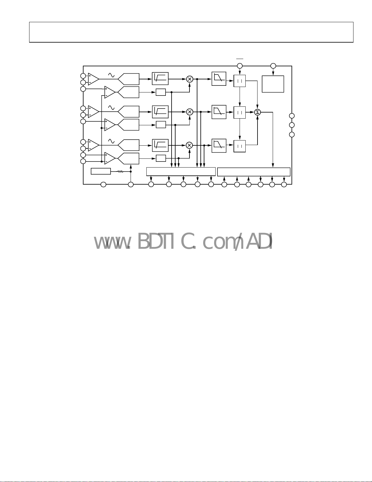
ADE7762
V
www.BDTIC.com/ADI
FUNCTIONAL BLOCK DIAGRAM
DD
5
POWER
SUPPLY
MONITOR
ADE7762
4
21
22
DGND
CLKIN
CLKOUT
IAP
IAN
VAP
IBP
IBN
VBP
ICP
ICN
VCP
VN
ABS
19
7
8
18
9
10
17
11
12
16
15
2.4V REF
4kΩ
ADC
ADC
ADC
ADC
ADC
ADC
HPF
Ф
HPF
Ф
HPF
Ф
PHASE AND REVP MONI TOR
LPF
LPF
LPF
DIGITAL -TO-FREQUENCY CONVERT ER
X
X
X
AGND
REF
1413
IN/OUT
6272821
25242320
3
26
CFS1 F1F2S0SCFREVPLED_CLED_BLED_ALED_CTRL
05757-001
Figure 1.
Rev. 0 | Page 3 of 28
Page 4

ADE7762
www.BDTIC.com/ADI
SPECIFICATIONS
VDD = 5 V ± 5%, AGND = DGND = 0 V, on-chip reference, CLKIN = 10 MHz, T
Table 1.
Parameter Conditions Min Typ Max Unit
ACCURACY
Measurement Error on Current
1, 2
Voltage channel with full-scale signal (±500 mV), 25°C,
Channel
over a dynamic range of 500 to 1
Phase Error Between Channels
PF = 0.8 Capacitive ±0.1 Degrees
PF = 0.5 Capacitive ±0.1 Degrees
AC Power Supply Rejection SCF = 0, S0 = S1 = 1
Output Frequency Variation (CF)
IA = IB = IC = 100 mV rms,
VA = VB = VC = 100 mV rms @ 50 Hz,
Ripple on V
of 200 mV rms @ 100 Hz
DD
DC Power Supply Rejection S1 = 1, S0 = SCF = 0
Output Frequency Variation (CF)
V1 = 100 mV rms, V2 = 100 mV rms,
= 5 V ± 250 mV
V
DD
ANALOG INPUTS See the Analog Inputs section
Maximum Signal Levels VAP – VN, VBP – VN, VCP – VN, IAP – IAN, IBP – IBN, ICP – ICN ±0.5
Input Impedance (DC) CLKIN = 10 MHz 370 410 kΩ
Bandwidth (−3 dB) CLKIN/256, CLKIN = 10 MHz 14 kHz
ADC Offset Error
1, 2
±25 mV
Gain Error External 2.5 V reference, IA = IB = IC = 500 mV dc ±9 % ideal
REFERENCE INPUT
REF
Input Voltage Range 2.4 V + 8% 2.6 V
IN/OUT
2.4 V − 8% 2.2 V
Input Impedance 3.3 kΩ
Input Capacitance 10 pF
ON-CHIP REFERENCE Nominal 2.4 V
Reference Error ±200 mV
Temperature Coefficient 25 ppm/°C
CLKIN (INPUT CLOCK FREQUENCY) All specifications for CLKIN of 10 MHz 10 MHz
LOGIC INPUTS3
ACF, S0, S1, and ABS
Input High Voltage, V
Input Low Voltage, V
V
INH
V
INL
= 5 V ± 5% 2.4 V
DD
= 5 V ± 5% 0.8 V
DD
Input Current, IIN Typically 10 nA, VIN = 0 V to VDD ±3 μA
Input Capacitance, CIN 10 pF
LOGIC OUTPUTS3
F1 and F2
Output High Voltage, VOH I
Output Low Voltage, VOL I
= 10 mA, V
SOURCE
= 10 mA, VDD = 5 V 0.5 V
SINK
= 5 V 4.5 V
DD
CF and REVP
Output High Voltage, VOH V
Output Low Voltage, VOL V
= 5 V, I
DD
= 5 V, I
DD
= 5 mA 4.5 V
SOURCE
= 5 mA 0.5 V
SINK
LED_CTRL VDD = 5 V, CLKIN = 10 MHz
Output Frequency 17.39 kHz
Output High Voltage VDD = 5 V, I
Output Low Voltage VDD = 5 V, I
= 10 mA 4.5 V
SOURCE
= 10 mA 0.4 V
SINK
LED_A, LED_B, LED_C
Output Low I
V
SINK
= 4.75 V 8 mA
DD
Output High Source VDD = 4.75 V 6 mA
MIN
to T
= −40°C to +85°C, unless otherwise noted.
MAX
0.1 % reading
0.01 % reading
0.1 % reading
V peak
difference
Rev. 0 | Page 4 of 28
Page 5
ADE7762
www.BDTIC.com/ADI
Parameter Conditions Min Typ Max Unit
POWER SUPPLY For specified performance
VDD 5 V ± 5% 4.75 5.25 V
IDD 8.5 10 mA
1
See the Terminology section for explanation of specifications.
2
See the plots in the Typical Performance Characteristics section.
3
Sample tested during initial release and after any redesign or process changes that might affect this parameter.
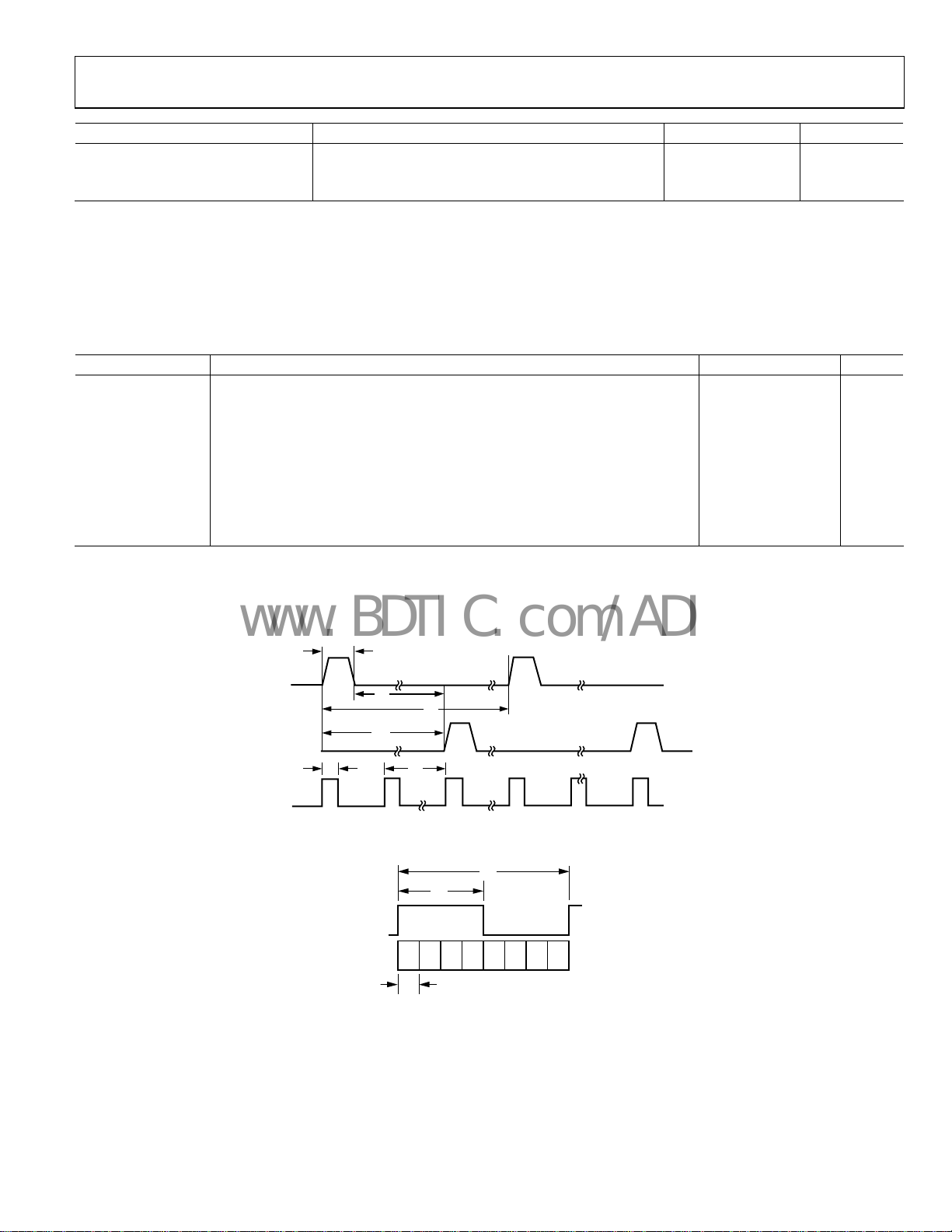
TIMING CHARACTERISTICS
VDD = 5 V ± 5%, AGND = DGND = 0 V, on-chip reference, CLKIN = 10 MHz, T
MIN
to T
= −40°C to +85°C, unless otherwise noted.
MAX
Table 2.
Parameter
3
t
F1 and F2 pulse width (logic high) 120 ms
1
1,2
Conditions Value Unit
t2 Output pulse period (see the Transfer Function section) See Figure 2 sec
t3 Time between F1 rising edge and F2 rising edge ½ t2 sec
3, 4
t
CF pulse width (logic high) 90 ms
4
5
t
CF pulse period (see the Transfer Function section) See Table 7 sec
5
t6 Minimum time between F1 and F2 pulse 4/CLKIN sec
t7 LED_CTRL pulse width 28.8 μs
t8 LED_CTRL period 57.5 μs
t9 LED pulse width 7.2 μs
1
Sample tested during initial release and after any redesign or process changes that might affect this parameter.
2
See Figure 2.
3
The pulse widths of F1, F2, and CF are not fixed for higher output frequencies (see the Frequency Outputs section).
4
CF is not synchronous to F1 or F2 frequency outputs.
5
The CF pulse is always 1 μs in the high frequency mode (see the Frequency Outputs section).
t
1
F1
t
6
t
2
t
F2
t
4
CF
3
t
5
05757-002
Figure 2. Timing Diagram for Frequency Outputs
t
8
t
7
LED1
LED2
LED3
t
9
Figure 3. Timing Diagram for LED Drivers
Rev. 0 | Page 5 of 28
NOT
LED4
USED
NOT
LED5
LED6
USED
05757-003
Page 6

ADE7762
www.BDTIC.com/ADI
ABSOLUTE MAXIMUM RATINGS
TA = 25°C, unless otherwise noted.
Table 3.
Parameter Rating
VDD to AGND −0.3 V to +7 V
VDD to DGND −0.3 V to +7 V
Analog Input Voltage to AGND
VA P, V BP, V C P, VN , I A P, IA N, IB P, I BN , I CP,
and ICN
Reference Input Voltage to AGND −0.3 V to VDD + 0.3 V
Digital Input Voltage to DGND −0.3 V to VDD + 0.3 V
Digital Output Voltage to DGND −0.3 V to VDD + 0.3 V
Operating Temperature Range, Industrial −40°C to +85°C
Storage Temperature Range −65°C to +150°C
Junction Temperature 150°C
28-Lead SOIC, Power Dissipation 63 mW
θJA Thermal Impedance 55°C/W
Lead Temperature, Soldering
Vapor Phase (60 sec) 215°C
Infrared (15 sec) 220°C
−6 V to +6 V
Stresses above those listed under Absolute Maximum Ratings
may cause permanent damage to the device. This is a stress
rating only; functional operation of the device at these or any
other conditions above those indicated in the operational
section of this specification is not implied. Exposure to absolute
maximum rating conditions for extended periods may affect
device reliability.
ESD CAUTION
Rev. 0 | Page 6 of 28
Page 7

ADE7762
www.BDTIC.com/ADI
PIN CONFIGURATION AND FUNCTION DESCRIPTIONS
Table 4. Pin Function Descriptions
Pin No. Mnemonic Description
1 LED_CTRL
LED Control Output. The LED_CTRL signal multiplexes the indication of phase drop, phase sequence
error, and per phase reverse power on the LED_A, LED_B, and LED_C pins.
2 LED_A
Phase A Phase Monitor Output. LEDs are connected to this pin to indicate phase drop or reverse power
on Phase A (see the Phase Monitor section).
3 CF
Calibration Frequency Logic Output. The CF logic output gives instantaneous active power information.
This output is intended to be used for calibration purposes.
4 DGND
This provides the ground reference for the digital circuitry in the ADE7762, that is, multipliers, filters,
and digital-to-frequency converters. Because the digital return currents in the ADE7762 are small, it is
acceptable to connect this pin to the analog ground plane of the whole system.
5 V
DD
Power Supply. This pin provides the supply voltage for the digital circuitry in the ADE7762. The supply
voltage should be maintained at 5 V ± 5% for a specified operation. This pin should be decoupled to
DGND with a 10 μF capacitor in parallel with a 100 nF ceramic capacitor.
6 REVP
This logic output goes logic high when negative power is detected on the sum of the three phase
powers. This output is not latched and resets when positive power is once again detected (see the
Negative Total Power Detection section).
7, 8;
9, 10;
11, 12
IAP, IAN;
IBP, IBN;
ICP, ICN
Analog Inputs for Current Channels. These channels are intended for use with current transducers and
are referenced in this document as current channels. These inputs are fully differential voltage inputs
with maximum differential input signal levels of ±0.5 V (see the Analog Inputs section). Both inputs
have internal ESD protection circuitry; in addition, an overvoltage of ±6 V can be sustained on these
inputs without risk of permanent damage.
13 AGND
This pin provides the ground reference for the analog circuitry in the ADE7762 (ADCs and reference).
This pin should be tied to the analog ground plane or the quietest ground reference in the system. This
quiet ground reference should be used for all analog circuitry, such as antialiasing filters and current
and voltage transducers. To keep ground noise around the ADE7762 to a minimum, the quiet ground
plane should connect to the digital ground plane at only one point. It is acceptable to place the entire
device on the analog ground plane.
14 REF
IN/OUT
This pin provides access to the on-chip voltage reference. The on-chip reference has a nominal value of
2.4 V ± 8% and a typical temperature coefficient of 25 ppm/°C. An external reference source can also be
connected at this pin. In either case, this pin should be decoupled to AGND with a 1 μF ceramic
capacitor.
15, 16, 17,
18
VN, VCP, VBP, VAP
Analog Inputs for the Voltage Channels. These channels are intended for use with voltage transducers
and are referenced in this document as voltage channels. These inputs are single-ended voltage inputs
with a maximum signal level of ±0.5 V with respect to VN for a specified operation. All inputs have
internal ESD protection circuitry; in addition, an overvoltage of ±6 V can be sustained on these inputs
without risk of permanent damage.
19
This logic input is used to select the method by which the three active energies from each phase are
ABS
summed. It selects between the arithmetical sum of the three energies (ABS
the absolute values (ABS
section.
20 SCF
Select Calibration Frequency. This logic input is used to select the frequency on the calibration output
CF. Table 7 shows how the calibration frequencies are selected.
LED_CTRL
LED_A
DGND
V
REVP
IAP
IAN
IBP
IBN
ICP
ICN
AGND
REF
IN/OUT
CF
DD
1
2
3
4
5
ADE7762
6
TOP VIEW
7
(Not to Scale)
8
9
10
11
12
13
14
28
27
26
25
24
23
22
21
20
19
18
17
16
15
LED_B
LED_C
F1
F2
S1
S0
CLKOUT
CLKIN
SCF
ABS
VAP
VBP
VCP
VN
05757-004
Figure 4. Pin Configuration
logic high) or the sum of
logic low). See the Mode Selection of the Sum of the Three Active Energies
Rev. 0 | Page 7 of 28
Page 8

ADE7762
www.BDTIC.com/ADI
Pin No. Mnemonic Description
21 CLKIN
22 CLKOUT
23, 24 S0, S1
25, 26 F2, F1
27 LED_C
28 LED_B
Master Clock for the ADCs and Digital Signal Processing. An external clock can be provided at this logic
input. Alternatively, a parallel resonant AT crystal can be connected across CLKIN and CLKOUT to
provide a clock source for the ADE7762. The clock frequency for the specified operation is 10 MHz.
Ceramic load capacitors between 22 pF and 33 pF should be used with the gate oscillator circuit. Refer
to the crystal manufacturer’s data sheet for the load capacitance requirements.
A crystal can be connected across this pin and CLKIN as described for Pin 21 to provide a clock source
for the ADE7762. The CLKOUT pin can drive one CMOS load when an external clock is supplied at CLKIN
or when a crystal is used.
These logic inputs are used to select one of four possible frequencies for the digital-to-frequency
conversion for design flexibility.
Low Frequency Logic Outputs. F1 and F2 supply average active power information. These logic outputs
can be used to drive electromechanical counters and 2-phase stepper motors directly (see the Transfer
Function section).
Phase C Phase Monitor Output. LEDs are connected to this pin to indicate phase drop or reverse power
on Phase C (see the Phase Monitor section).
Phase B Phase Monitor Output. LEDs are connected to this pin to indicate phase drop or reverse power
on Phase B (see the Phase Monitor section).
Rev. 0 | Page 8 of 28
Page 9
ADE7762
www.BDTIC.com/ADI
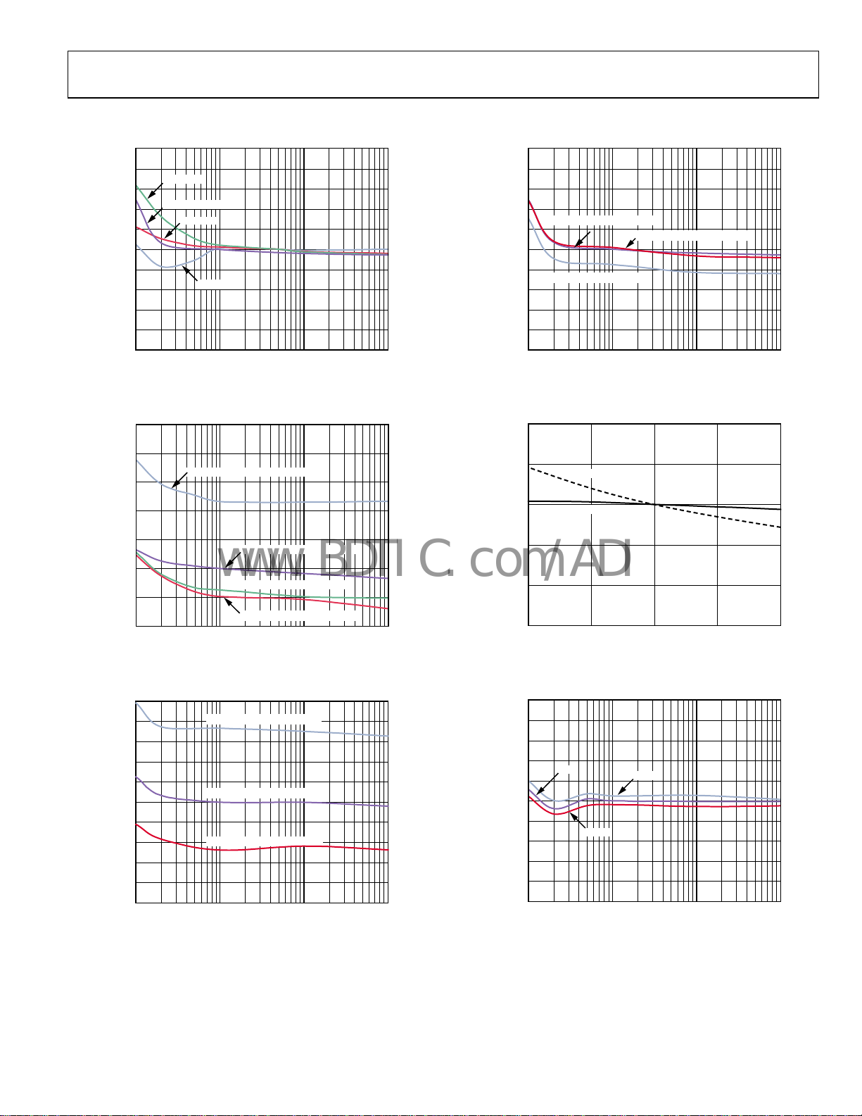
TYPICAL PERFORMANCE CHARACTERISTICS
0.5
0.4
0.3
0.2
0.1
% ERROR
–0.1
–0.2
–0.3
–0.4
–0.5
PHASE C
PHASE A + B + C
PHASE B
0
PHASE A
0.1 1 10 100
CURRENT CHANNEL (% of Full Scale)
Figure 5. Error As a Percent of Reading
with Internal Reference (Wye Connection)
1.0
05757-007
0.5
0.4
0.3
0.2
+25°C, POW ER FACTOR = 1
0.1
0
% ERROR
–0.1
–40°C, POW ER FACTOR = 1
–0.2
–0.3
–0.4
–0.5
0.1 1 10 100
CURRENT CHANNEL (% of Full Scale)
+85°C, POW ER FACTOR = 1
Figure 8. Error As a Percent of Reading over Temperature
with External Reference (Wye Connection)
1.0
05757-010
0.8
0.6
0.4
0.2
% ERROR
0
–0.2
–0.4
0.1 1 10 100
–40°C, POW ER FACTO R = 0.5
+25°C, POW ER FACTOR = 1
+25°C, POW ER FACTOR = 0.5
+85°C, POWER FACTO R = 0.5
CURRENT CHANNEL (% of Full Scale)
Figure 6. Error As a Percent of Reading over Power Factor
with Internal Reference (Wye Connection)
1.0
0.8
0.6
0.4
0.2
0
% ERROR
–0.2
–0.4
–0.5
–0.8
–1.0
0.1 1 10 100
–40°C, POW ER FACTOR = 1
+25°C, POW ER FACTOR = 1
+85°C, POW ER FACTOR = 1
CURRENT CHANNEL (% of Full Scale)
Figure 7. Error As a Percent of Reading over Temperature
with Internal Reference (Wye Connection)
0.5
0
% ERROR
–0.5
–1.0
05757-008
–1.5
POWER FACT OR = 1
POWER FACT OR = 0.5
45 50 55 60 65
LINE FREQ UENCY (Hz)
05757-011
Figure 9. Error As a Percent of Reading over Frequency
with an Internal Reference (Wye Connection)
0.5
0.4
0.3
0.2
0.1
% ERROR
–0.1
–0.2
–0.3
–0.4
05757-009
–0.5
5V
0
5.25V
0.1 1 10 100
CURRENT CHANNEL (% of Full Scale)
4.75V
05757-012
Figure 10. Error As a Percent of Reading over Power Supply
with Internal Reference (Wye Connection)
Rev. 0 | Page 9 of 28
Page 10

ADE7762
V
V
www.BDTIC.com/ADI
TEST CIRCUIT
DD
1kΩ
33nF
1kΩ
33nF
100nF
7
8
9
10
11
12
18
17
16
15
IAP
IAN
IBP
IBN
ICP
ICN
VAP
VBP
VCP
VN
5
19
V
ABS
DD
ADE7762
CLKOUT
REF
LED_CTRL
AGND DGND
13
CF
CLKIN
SCF
IN/OUT
REVP
LED_A
LED_B
LED_C
4
26
F1
25
F2
820Ω
3
22
10MHz
21
23
S0
24
S1
20
14
0.1µF 10µF
6
1
2
28
27
22pF
22pF
1kΩ
1
23
V
DD
4
TO
FREQUENCY
COUNTER
K7
K8
05757-015
220
AC
1MΩ
1kΩ
I
LOAD
33nF
10µF
Rb
SAME AS
IAP, IAN
SAME AS
IAP, IAN
SAME AS VAP
SAME AS VAP
33nF
1kΩ
Figure 11. Test Circuit for Performance Curves
Rev. 0 | Page 10 of 28
Page 11

ADE7762
www.BDTIC.com/ADI
TERMINOLOGY
Measurement Error
The error associated with the energy measurement made by the
ADE7762 is defined by the following formula:
Percentage Error =
⎛
⎜
⎜
⎝
Error Between Channels
The high-pass filter (HPF) in the current channel has a phase
lead response. To offset this phase response and equalize the
phase response between channels, a phase correction network
is placed in the current channel. The phase correction network
ensures a phase match between the current channels and the
voltage channels to within ±0.1° over a range of 45 Hz to 65 Hz
and ±0.2° over a range of 40 Hz to 1 kHz (see Figure 24 and
Figure 25).
Power Supply Rejection (PSR)
This quantifies the ADE7762 measurement error as a percentage of reading when the power supplies are varied.
For the ac PSR measurement, a reading at a nominal supply
(5 V) is taken. A 200 mV rms/100 Hz signal is then introduced
onto the supply, and a second reading is obtained under the
same input signal levels. Any error introduced is expressed as a
percentage of reading. See the definition for Measurement Error.
For the dc PSR measurement, a reading at nominal supplies
(5 V) is taken. The supply is then varied ±5%, and a second
reading is obtained with the same input signal levels. Any
error introduced is again expressed as a percentage of reading.
yTrue Energ
yTrue Energ– ADE7762istered byEnergy Reg
⎞
⎟
%100
×
⎟
⎠
(1)
ADC Offset Error
This refers to the dc offset associated with the analog inputs
to the ADCs. It means that with the analog inputs connected
to AGND, the ADCs still see an analog input signal offset.
However, because the HPF is always present, the offset is removed from the current channel, and the power calculation
is not affected by this offset.
Gain Error
The gain error of the ADE7762 is defined as the difference
between the measured output frequency (minus the offset)
and the ideal output frequency. The difference is expressed
as a percentage of the ideal frequency. The ideal frequency is
obtained from the ADE7762 transfer function (see the Transfer
Function section).
Rev. 0 | Page 11 of 28
Page 12

ADE7762
www.BDTIC.com/ADI
THEORY OF OPERATION
The six signals from the current and voltage transducers are
digitized with ADCs. These ADCs are 16-bit, second-order
∑-Δ devices with an oversampling rate of 833 kHz. This analog
input structure greatly simplifies transducer interface by
providing a wide dynamic range and bipolar input for direct
connection to the transducer. High-pass filters in the current
channels remove the dc component from the current signals.
This eliminates any inaccuracies in the active power calculation
due to offsets in the voltage or current signals (see the HPF and
Offset Effects section).
The active power calculation is derived from the instantaneous
power signal. The instantaneous power signal is generated by a
direct multiplication of the current and voltage signals of each
phase. To extract the active power component, the dc component, the instantaneous power signal is low-pass filtered on
each phase. Figure 12 illustrates the instantaneous active power
signal and shows how the active power information can be
extracted by low-pass filtering the instantaneous power signal.
This method is used to extract the active power information
on each phase of the polyphase system. The total active power
information is then obtained by adding the individual phase
active power. This scheme correctly calculates active power
for nonsinusoidal current and voltage waveforms at all power
factors. All signal processing is carried out in the digital domain
for superior stability over temperature and time.
The low frequency output of the ADE7762 is generated by
accumulating the total active power information. This low
frequency inherently means a long accumulation time between
output pulses. The output frequency is therefore proportional to
the average active power. This average active power information
can, in turn, be accumulated (for example, by a counter) to
generate active energy information. Because of its high output
frequency and, therefore, shorter integration time, the CF
output is proportional to the instantaneous active power. This
pulse is useful for system calibration purposes that take place
under steady load conditions.
POWER FACTOR CONSIDERATIONS
Low-pass filtering, the method used to extract the active power
information from the individual instantaneous power signal, is
still valid when the voltage and current signals of each phase are
not in phase. Figure 13 displays the unity power factor condition
and a displacement power factor (DPF) of 0.5, that is, current
signal lagging the voltage by 60° for one phase of the polyphase.
Assuming that the voltage and current waveforms are sinusoidal, the active power component of the instantaneous power
signal (the dc term) is given by
×
1V
⎞
⎛
⎜
2
⎝
This is the correct active power calculation.
⎟
⎠
()
°×
60cos
(2)
p(t) = i(t) × v(t)
V×I
V×I
IAP
IAN
VAP
IBP
IBN
VBP
ICP
ICN
VCP
VN
2
TIME
WHERE:
v(t) = V × cos (ωt)
i(t) = I × cos (ωt)
p(t) = V × I
POWER SIGNAL - p(t)
ADC
ADC
ADC
ADC
ADC
ADC
{1+ cos (2ωt)}
2
INSTANTANEOUS
HPF
MULTIPLIER
HPF
MULTIPLIER
HPF
MULTIPLIER
V × I
2
INSTANTANEOUS
ACTIVE POWER SIGNAL
ABS
LPF
|X|
LPF
|X|
LPF
|X|
Figure 12. Signal Processing Block Diagram
VA × IA + VB × IB +
VC × IC
2
INSTANTANEO US
TOTAL POWER
SIGNAL
DIGITAL-TO-FREQUENCY
DIGITAL-TO-FREQUENCY
F1
F2
CF
05757-016
Rev. 0 | Page 12 of 28
Page 13

ADE7762
(
)
×
=
V
www.BDTIC.com/ADI
V× I
2
V× I
2
0V
×cos(60°)
0V
Figure 13. DC Component of Instantaneous Power Signal
INSTANTANEO US
POWER SI GNAL
CURRENT
VOLTAGE
INSTANTANE OUS
POWER SI GNAL
VOLTAGE
INSTANTANEO US
ACTIVE PO WER SIGNAL
60°
INSTANTANEO US
ACTIVE PO WER SIGNAL
CURRENT
NONSINUSOIDAL VOLTAGE AND CURRENT
The active power calculation method also holds true for
nonsinusoidal current and voltage waveforms. All voltage and
current waveforms in practical applications have some harmonic content. Using the Fourier transform, instantaneous
voltage and current waveforms can be expressed in terms of
their harmonic content
∞
O
∑
n
=
0
where:
v(t) is the instantaneous voltage.
is the average value.
V
O
V
is the rms value of voltage harmonic n.
n
is the phase angle of the voltage harmonic.
α
n
()
sin2)(
n
αtnVVtv +ω××+=
(3)
n
() ()
O
∞
∑
n
sin2
n
1
=
()
βtnIIti ω××+=
(4)
n
where:
i(t) is the instantaneous current.
is the dc component.
I
O
is the rms value of current harmonic n.
I
n
β
is the phase angle of the current harmonic.
n
Using Equation 3 and Equation 4, the active power, P, can be
expressed in terms of its fundamental active power (P
harmonic active power (P
P = P
+ PH
1
).
H
) and
1
where:
φcos
P
φ
05757-017
H
n
φ
I
1111
β−α=
∞
∑
n
1
=
n
β−α=
(5)
111
IVP
×=
nn
φcos
nn
(6)
As can be seen from Equation 6, a harmonic active power
component is generated for every harmonic, provided that
harmonic is present in both the voltage and current waveforms.
The power factor calculation has been shown to be accurate in
the case of a pure sinusoid. Therefore, the harmonic active
power also correctly accounts for power factor because
harmonics are made up of a series of pure sinusoids. A limiting
factor on harmonic measurement is the bandwidth. On the
ADE7762, the bandwidth of the active power measurement is
14 kHz with a master clock frequency of 10 MHz.
Rev. 0 | Page 13 of 28
Page 14

ADE7762
V
www.BDTIC.com/ADI
ANALOG INPUTS
CURRENT CHANNELS
The voltage outputs from the current transducers are connected
to the ADE7762 current channels, which are fully differential
voltage inputs. IAP, IBP, and ICP are the positive inputs for IAN,
IBN, and ICN, respectively.
The maximum peak differential signal on the current channel
should be less than ±500 mV (353 mV rms for a pure sinusoidal
signal) for the specified operation.
IAP–IAN
+500mV
DIFFERENTIAL INPUT
V
CM
–500mV
Figure 14. Maximum Signal Levels, Current Channel
±500mV MAX PEAK
COMMON-MO DE
±25mV MAX
AGN D
The maximum signal levels on IAP and IAN are shown in
Figure 14. The maximum differential voltage between IAP
and IAN is ±500 mV. The differential voltage signal on the
inputs must be referenced to a common mode, for example,
AGND. The maximum common-mode signal shown in
Figure 14 is ±25 mV.
IAP
IA
IAN
V
CM
05757-018
VOLTAGE CHANNELS
The output of the line voltage transducer is connected to the
voltage inputs of the ADE7762. Voltage channels are pseudodifferential voltage inputs. VAP, VBP, and VCP are the positive
inputs with respect to VN.
The maximum peak differential signal on the voltage channel is
±500 mV (353 mV rms for a pure sinusoidal signal) for a specified operation.
Figure 15 illustrates the maximum signal levels that can be
connected to the ADE7762 voltage channels.
AP–VN
+500mV
DIFFERENTIAL INPUT
V
CM
–500mV
Figure 15. Maximum Signal Levels, Voltage Channel
±500mV MAX PEAK
COMMON-MODE
±25mV MAX
AGND
Voltage channels must be driven from a common-mode voltage,
that is, the differential voltage signal on the input must be referenced to a common mode (usually AGND). The analog inputs
of the ADE7762 can be driven with common-mode voltages of
up to 25 mV with respect to AGND. However, best results are
achieved using a common mode equal to AGND.
VA
VCM
VAP
VN
05757-019
Rev. 0 | Page 14 of 28
Page 15

ADE7762
(
(
(
)
(
)
+ω××−××=
(
=
www.BDTIC.com/ADI
TYPICAL CONNECTION DIAGRAMS
CURRENT CHANNEL CONNECTION
Figure 16 shows a typical connection diagram for the current
channel (IAN). A current transformer (CT) is the current transducer selected for this example. Notice that the common-mode
voltage for the current channel is AGND and is derived by
center-tapping the burden resistor to AGND. This provides the
complementary analog input signals for IAP and IAN. The CT
turns ratio and Burden Resistor Rb are selected to give a peak
differential voltage of ±500 mV at maximum load.
In theory, it is better to center-tap Rb; however, this requires
very careful attention to the layout and matching of the resistors
to ensure that the channels have the same resistance. A single
resistor may be more practical and is a valid design choice.
CT
IP
NEUTRALPHASE
Figure 16. Typical Connection for Current Channels
Rf
Rb
±500mV
Rf
IAP
Cf
IAN
Cf
05757-020
METER CONNECTIONS
In 3-phase service, two main power distribution services exist:
3-phase, 4-wire or 3-phase, 3-wire. The additional wire in the
3-phase, 4-wire arrangement is the neutral wire. The voltage
lines have a phase difference of ±120° (±2π/3 radians) between
each other (see Equation 7).
()
()
()
where V
different phases.
The current inputs are represented by
, VB, and VC represent the voltage rms values of the
A
()
()
AA
BB
()
tVtV
AA
BB
CC
ω××= cos2
l
π
2
⎛
cos2 tVtV
⎜
⎝
⎛
cos2 tVtV
⎜
⎝
tItI φcos2 +ω×=
l
⎛
tItI φ
cos2 (8)
⎜
l
⎝
⎞
(7)
+ω××=
⎟
l
3
⎠
π
4
⎞
+ω××=
⎟
l
3
⎠
)
A
2
π
⎞
+
+ω×=
3
⎟
B
⎠
VOLTAGE CHANNEL CONNECTION
Figure 17 shows two typical connections for the voltage channel. The first option uses a potential transformer (PT) to provide complete isolation from the main voltage. In the second
option, the ADE7762 is biased around the neutral wire, and a
resistor divider is used to provide a voltage signal proportional
to the line voltage. Adjusting the ratio of Ra, Rb, and VR is a
convenient way of carrying out a gain calibration on the meter.
VR can be implemented using either a potentiometer or a
binary weighted series of resistors. Either configuration works,
however, the potentiometer is subject to noise over time. Two
fixed value resistors can be used in place of VR to minimize
the noise.
PT
±500mV
AGN D
NEUTRALPHASE
Ra*
NEUTRALPHAS E
Figure 17. Typical Connections for Voltage Channels
Cf
Rb*
±500mV
VR*
*Ra >> Rf + VR; *Rb + VR = Rf
Rf
Rf
Rf
VAP
Cf
VN
Cf
VAP
VN
Cf
4
π
()
⎛
tItI φ
cos2
CC
+ω×=
⎜
l
⎝
⎞
+
⎟
C
3
⎠
where:
I
, IB, and IC represent the rms value of the current of each
A
phase.
, φB, and φC represent the phase difference of the current and
φ
A
voltage channel of each phase.
The instantaneous powers can then be calculated as follows:
P
(t) = VA(t) × IA(t)
A
(t) = VB(t) × IB(t)
P
B
P
(t) = VC(t) × IC(t)
C
Then,
B
)
)
tP
()
()
()
AAAAAA
⎛
tIVIV φ
2cosφcos (9)
⎜
BBBBB
l
⎝
CCCCCC
+ω××−××
⎛
⎜
⎝
l
π
4
+
3
tIVIVtP φ
2cosφcos
l
tIVIVtP φ2cosφcos
A
⎞
⎟
B
⎠
π
8
+ω××−××=
⎞
+
⎟
C
3
⎠
As shown in Equation 9, the active power calculation per phase
is made when current and voltage inputs of one phase are
connected to the same channel (A, B, or C). Then the
05757-021
summation of each individual active power calculation gives the
total active power information,
P(t) = P
(t) + PB(t) + PC(t).
A
Rev. 0 | Page 15 of 28
Page 16

ADE7762
www.BDTIC.com/ADI
Figure 18 shows the connections of the ADE7762 analog inputs
with the power lines in a 3-phase, 3-wire delta service.
Cf
Ra*
Rb*
VAP
IAP
IAN
VN
Cf
IBP
IBN
VBP
LOAD
PHASE A
SOURCE
PHASE B
VR*
Ra*
Rb*
VR*
Rb*
CT
PHASE C
Cf
*Ra >> Rf + VR; *Rb + VR = Rf
ANTIALIASING
CT
Rb*
FILTERS
Rf
ANTIALIASING
FILTERS
Figure 18. 3-Phase, 3-Wire Meter Connection with ADE7762
Note that only two current inputs and two voltage inputs of the
ADE7762 are used in this case. The active power calculated by
the ADE7762 does not depend on the selected channels.
05757-022
Figure 19 shows the connections of the ADE7762 analog inputs
with the power lines in a 3-phase, 4-wire Wye service.
Cf
Ra*
Rb*
PHASE A
SOURCE
Rf
VR*
PHASE B
PHASE C
Ra*
Rb*
VR*
CF
Rb*
CT
Cf
Ra*
Rb*
VR*
CT
Cf
VN
Rb*
*Ra >> Rf + VR;*Rb + VR = Rf
ANTIALIASING
FILTERS
ANTIALI ASING
FILTERS
CT
Rb*
VAP
IAP
IAN
ANTIALIASING
FILTERS
ICP
LOAD
ICN
VCP
IBP
IBN
VBP
Figure 19. 3-Phase, 4-Wire Meter Connection with ADE7762
05757-023
Rev. 0 | Page 16 of 28
Page 17

ADE7762
www.BDTIC.com/ADI
POWER SUPPLY MONITOR
The ADE7762 contains an on-chip power supply monitor. The
power supply (V
when the supply is less than 4 V ± 2% and V
) is monitored continuously. At power-up,
DD
is less than 1.9 V
REF
(typical), the outputs of the ADE7762 are inactive and the data
path is held in reset. Once VDD is greater than 4 V ±2% and
VREF is greater than 1.9 V (typical), the chip is active and energy
accumulation begins. At power-down, when VDD falls below
4 V or V
falls below 1.9 V (typical), the data path is again held
REF
in reset. This implementation ensures correct device operation
at power-up and at power-down. The power supply monitor
has built-in hysteresis and filtering. This gives a high degree of
immunity to false triggering due to noisy supplies.
The power supply and decoupling for the part should be such
that the ripple at V
does not exceed ±5% as specified for
DD
normal operation.
2.4V
1.9V
INTERNAL
RESET
5V
4V
0V
INACTIVE
Figure 20. On-Chip Power Supply Monitor
V
DD
V
REF
ACTIVE INACTIVE
05757-024
Rev. 0 | Page 17 of 28
Page 18

ADE7762
www.BDTIC.com/ADI
PHASE MONITOR
The ADE7762 has phase monitoring functions to detect phase
dropout, phase sequence error, and reverse polarity using four
pins. Phase dropout has the highest priority, and reverse
polarity has the lowest priority. If a phase dropout occurs, phase
sequence error indication is disabled until all three phases are
above the phase dropout level (see the Phase Dropout Error
section). Because the dropout detection level is not set to zero, a
phase can have some small voltage during a phase dropout
condition. Therefore, reverse polarity is still indicated on that
phase if the proper conditions occur.
The phase monitor circuit functions by multiplexing signals onto
the four pins. The four multiplexed pins are LED_CTRL, LED_A,
LED_B, and LED_C. Two LEDs can be connected to each pin as
shown in Figure 21. When LED_CTRL is high, LED_A is low to
turn on an LED and indicate a phase drop condition on Phase A.
When LED_CTRL is low, LED_A is high to indicate a reverse
polarity (REVP) condition on Phase A. Phase sequence error is
indicated by blinking the Phase Seq/Drop LEDs.
LED_CTRL switches at a rate of 131 kHz so that both the Phase
Seq/Drop LEDs and REVP LEDs can appear to be on simultaneously, which allows indication of phase dropout and REVP at the
same time. For the timing diagram, see Figure 3.
LOAD
LED_CTRL
LED_A
LED_B
LED_C
05757-025
PHASE
SEQ/DROP
PHASE
SEQ/DROP
PHASE
SEQ/DROP
REVP
R
REVP
R
LOAD
Figure 21. Phase Monitor Circuit
LOAD
REVP
R
PHASE DROPOUT ERROR
The ADE7762 indicates a phase drop condition when there is a
low voltage signal or no voltage signal on a phase. The phase
dropout condition occurs when the amplitude of the phase
drops below 20% of full-scale analog input voltage or when a
zero crossing is not followed by another zero crossing on that
phase for 150 ms. When this occurs, a phase dropout signal is
generated, and the Phase Seq/Drop LED is turned on for the
missing phase. The delay between the phase drop condition
occurring at the analog inputs and indication of the condition
on the LED outputs is approximately 150 ms. During a phase
dropout condition, energy continues to accumulate on the
dropped channel, as well as the other channels, and phase
sequence error indication is disabled. The Phase Seq/Drop LED
for the dropped phase is turned off when the zero crossings
return for more than 150 ms and there is more than 20% of fullscale input voltage on the voltage input of that phase.
PHASE SEQUENCE ERROR
The ADE7762 detects the zero crossing of each phase. A phase
sequence error occurs when the sequence A>B>C>A> … is
violated. If a phase sequence error occurs, the Phase Seq/Drop
LEDs blink at 1 Hz (see Figure 22).
Phase sequence error and REVP can be displayed simultaneously. The REVP LEDs continue to indicate reverse polarity if
the proper conditions exist. For example, if the phase sequence
becomes A>C>B>A… and Phase B has negative active energy
accumulated, then the REVP LED for Phase B is on solid, and
all of the Phase Seq/Drop LEDs are blinking at 1 Hz. The delay
in indicating the phase sequence error with blinking LEDs is
approximately 150 ms from the time that a phase sequence
error occurs.
Rev. 0 | Page 18 of 28
PHASE REVERSE POLARITY DETECTION
When reverse power is detected on any phase, the corresponding REVP LED turns on for that phase. For example, if the
power for Phase A is negative, the REVP LED connected to
LED_A turns on. The indication of REVP on the LED_A,
LED_B, or LED_C pins is nearly instantaneous. As soon as the
input to the ADCs changes and the power is calculated such
that there is a reverse power condition on any phase, the
appropriate LED is turned on.
Page 19

ADE7762
W
W
W
www.BDTIC.com/ADI
80% FS
VOLTAGE
AVEFORMS
RISING EDG E
ZERO
CROSSINGS
80% FS
VOLTAGE
AVEFORMS
RISING EDG E
ZERO
CROSSINGS
80% FS
A = 0°
AB C
A = 0°
AC B
PHASE SEQ/ DROP LEDS ARE BLINKING AT 1Hz.
A = 0°
B = –120°
PHASE SEQ/ DROP LEDS ARE OFF.
C = –120°
C = +120°
B = +120°
A
C = –120°
BA
C
C
B
20% FS
VOLTAGE
AVEFORMS
RISING EDG E
ZERO
CROSSINGS
AB C
PHASE SEQ/ DROP LED F OR PHASE B I S ON.
B = +120°
A
B
C
05757-030
Figure 22. Phase Sequence Detection
Rev. 0 | Page 19 of 28
Page 20

ADE7762
(
)
(
)
(
)
(
)
www.BDTIC.com/ADI
HPF AND OFFSET EFFECTS
Figure 23 shows the effect of offsets on the active power
calculation. An offset on the current channel and the voltage
channel contributes a dc component after multiplication, as
shown in Figure 23. Because this dc component is extracted by
the LPF and is used to generate the active power information
for each phase, the offsets can contribute a constant error to the
total active power calculation. The HPF in the current channels
avoids this problem easily. By removing the offset from at least
one channel, no error component can be generated at dc by the
multiplication. Error terms at cos(ωt) are removed by the LPF
and the digital-to-frequency conversion (see the Digital-toFrequency Conversion) section.
coscos
IV
×
2
IV
×
+
2
()
t
ω×
2cos
ItIVtV
=+ω×+ω
OSOS
() ()
OSOSOSOS
tVItIVIV
ω×+ω×+×+
coscos
(10)
The ADE7762 is phase compensated up to 1 kHz as shown. This
ensures correct active harmonic power calculation even at low
power factors.
0.07
0.06
0.05
0.04
0.03
0.02
PHASE (Degrees)
0.01
0
–0.01
0.010
100 300 500 700 900
0 1000200 400 600 800
Figure 24. Phase Error Between Channels (0 Hz to 1 kHz)
FREQUENCY (Hz)
05757-031
DC COMPONENT (INCLUDING ERROR TERM)
VOS×I
OS
V×I
2
Figure 23. Effect of Channel Offset on the Active Power Calculation
IS EXTRACTED BY THE LPF FOR REAL
POWER CALCULAT ION
IOS×V
×I
V
OS
0
ω
FREQUENCY – RAD/S
2
ω
05757-026
The HPF in the current channels has an associated phase response
that is compensated for on-chip. Figure 24 and Figure 25 show the
phase error between channels with the compensation network.
0.008
0.006
0.004
0.002
PHASE (Degrees)
0
–0.002
–0.004
40 7045 50
Figure 25. Phase Error Between Channels (40 Hz to 70 Hz)
55 60 65
FREQUENCY (Hz)
05757-032
Rev. 0 | Page 20 of 28
Page 21

ADE7762
www.BDTIC.com/ADI
DIGITAL-TO-FREQUENCY CONVERSION
After multiplication, the digital output of the low-pass filter
contains the active power information of each phase. However,
because this LPF is not an ideal brick wall filter implementation,
the output signal also contains attenuated components at the line
frequency and its harmonics, that is, cos(hωt), where h = 1, 2, 3 …
The magnitude response of the filter is given by
()
||
1
=ffH (11)
1
2
⎫
⎧
+
⎬
⎨
8
⎭
⎩
where the −3 dB cutoff frequency of the low-pass filter is 8 Hz.
For a line frequency of 50 Hz, this gives an attenuation of
the 2ω (100 Hz) component of approximately −22 dB. The
dominating harmonic is twice the line frequency, that is,
cos(2ωt), due to the instantaneous power signal. Figure 26
shows the instantaneous active power signal at the output of
the CF, which still contains a significant amount of instantaneous power information, cos(2ωt).
This signal is then passed to the digital-to-frequency converter
where it is integrated (accumulated) over time to produce an
output frequency. This accumulation of the signal suppresses or
averages out any nondc component in the instantaneous active
power signal.
VA
MULTIPLIER
IA
VB
MULTIPLIER
IB
ABS
LPF
|X|
LPF
|X|
Σ
The average value of a sinusoidal signal is zero. Thus, the
frequency generated by the ADE7762 is proportional to the
average active power. Figure 26 shows the digital-to-frequency
conversion for steady load conditions, that is, constant voltage
and current.
The frequency output CF varies over time, even under steady load
conditions (see Figure 26). This frequency variation is primarily
due to the cos(2ωt) components in the instantaneous active power
signal. The output frequency on CF can be up to 160× higher than
the frequency on F1 and F2. The higher output frequency is
generated by accumulating the instantaneous active power signal
over a much shorter time, while converting it to a frequency. This
shorter accumulation period means less averaging of the cos(2ωt)
component. Therefore, some of this instantaneous power signal
passes through the digital-to-frequency conversion.
Where CF is used for calibration purposes, the frequency counter
should average the frequency to remove the ripple and obtain a
stable frequency. If CF is used to measure energy, for example, in a
microprocessor-based application, the CF output should also be
averaged to calculate power. Because the outputs F1 and F2 operate
at a much lower frequency, significant averaging of the
instantaneous active power signal is carried out. The result is a
greatly attenuated sinusoidal content and a virtually ripple-free
frequency output on F1 and F2, which are used to measure energy
in a stepper motor-based meter.
F1
DIGITAL-TO -
FREQUENCY
Σ
DIGITAL-TO -
FREQUENCY
Σ
F1
F2
FREQUENCY
TIME
CF
CF
VC
MULTIPLIER
IC
LPF
|X|
LPF TO EXTRACT
REAL POWER
(DC T ERM )
Figure 26. Active Power-to-Frequency Conversion
Rev. 0 | Page 21 of 28
FREQUENCY
TIME
V× I
2
cos(2ωt)
ATT E NU ATE D BY LP F
0
INSTANTANEOUS REAL POWER S IGNAL
ω
FREQUENCY – RAD/S
(FREQUENCY DOMAIN)
2ω
05757-029
Page 22

ADE7762
www.BDTIC.com/ADI
ACCUMULATION OF 3-PHASE POWER
Power Measurement Considerations
Calculating and displaying power information always have
some associated ripple that depends on the integration period
used in the MCU to determine average power as well as the
load. For example, at light loads, the output frequency can be
10 Hz. With an integration period of 2 seconds, only about
20 pulses are counted. The possibility of missing one pulse
always exists because the ADE7762 output frequency is running
asynchronously to the MCU timer. This results in a 1-in-20
or 5% error in the power measurement. To remedy this, an
appropriate integration time should be considered to achieve
the desired accuracy.
Mode Selection of the Sum of the Three Active Energies
The ADE7762 can be configured to execute the arithmetic sum
of the three active energies, Wh = Wh
sum of the absolute value of these energies, Wh = |Wh
|Wh
| + |WhΦC|. The selection between the two modes can be
ΦB
made by setting the
ABS
on the
of absolute values, respectively.
When the sum of the absolute values is selected, the active
energy from each phase is always counted positive in the total
active energy. It is particularly useful in 3-phase, 4-wire installation where the sign of the active power should always be the
pin correspond to the arithmetic sum and the sum
ABS
pin. Logic high and logic low applied
+ WhΦB + WhΦC, or the
ΦA
| +
ΦA
same. If the meter is misconnected to the power lines, that is,
if CT is connected in the wrong direction, then the total active
energy recorded without this solution can be reduced by
two-thirds.
The sum of the absolute values assures that the active energy
recorded represents the actual active energy delivered. In this
mode, the reverse power pin still detects when the arithmetic
sum of the active powers is negative, but energy continues to
accumulate regardless of the sign.
Negative Total Power Detection
The ADE7762 detects when total power, calculated as the
arithmetic sum of the three phases, is negative. This detection
is independent of the mode of the sum of the three powers
(arithmetic or absolute). This mechanism can detect an incorrect connection of the meter or generation of negative active
energy. When the sum of the powers of the three phases is
negative, the REVP pin output goes active high. When the
sum of the powers of the three phases is positive, the REVP
pin output is reset to low.
The REVP pin output changes state at the same time that a
pulse is issued on CF. If the sum of the powers of the three
phases is negative, then the REVP pin output stays high until
the sum of the three phases’ power is positive or until all three
phases are below the no-load threshold.
Rev. 0 | Page 22 of 28
Page 23

ADE7762
(
)
×
=
×
(
()()(
)
www.BDTIC.com/ADI
TRANSFER FUNCTION
FREQUENCY OUTPUTS F1 AND F2
The ADE7762 calculates the product of six voltage signals (on
current channel and voltage channel) and then low-pass filters
this product to extract active power information. This active
power information is then converted to a frequency. The
frequency information is output on F1 and F2 in the form of
active high pulses. The pulse rate at these outputs is relatively
low, for example, 2.09 Hz maximum for ac signals with SCF =
S0 = 0; S1 = 1 (see Table 6). This means that the frequency at
these outputs is generated from active power information
accumulated over a relatively long period. The result is an
output frequency that is proportional to the average active
power. The averaging of the active power signal is implicit to
the digital-to-frequency conversion. The output frequency or
pulse rate is related to the input voltage signals by the following
equation:
Freq
313.6
=
AAN
BBN
2
V
REF
×+×+××
(12)
where:
Freq is the output frequency on F1 and F2 (Hz).
V
, VBN, and VCN are the differential rms voltage signal on
AN
voltage channels (V).
, IB, and IC are the differential rms voltage signal on current
I
A
channels (V).
is the reference voltage (2.4 V ± 8%) (V).
V
REF
f
is one of seven possible frequencies selected by using the
1 to 7
logic inputs SCF, S0, and S1 (see Table 5).
Table 5. f
SCF S1 S0 f
0 0 0 2.24
1 0 0 4.49
0 0 1 1.12
1 0 1 4.49
0 1 0 5.09
1 1 0 1.12
0 1 1 0.56
1 1 1 0.56
1
f
is a fraction of the master clock and therefore varies if the specified
1 to 7
CLKIN frequency is altered.
Frequency Selection1
1 to 7
1 to 7
(Hz)
fIVIVIV
CCN
7to1
Example 1
In this example, with ac voltages of ±500 mV peak applied to
the voltage channels and current channels, the expected output
frequency is calculated as follows:
1,Hz56.0
S1S0SCFf
7to1
BN
AN
CN
acpeakmV500
()
=
V
REF
===
ICIBIAVVV
=====
5.0
==
2
(13)
rmsV
valuereferencenominalV4.2
Note that if the on-chip reference is used, actual output frequencies can vary from device to device due to a reference
tolerance of ±8%.
58.05.05.0313.6
×=Freq (14)
3
××
2
4.222
××
Hz230.0
=
As can be seen from these two example calculations, the maximum
output frequency for ac inputs is always half of that for dc input
signals. The maximum frequency also depends on the number
of phases connected to the ADE7762. In a 3-phase, 3-wire delta
service, the maximum output frequency is different from the maximum output frequency in a 3-phase, 4-wire Wye service. The
reason is that there are only two phases connected to the analog
inputs, but also that in a delta service, the current channel input
and voltage channel input of the same phase are not in phase in
normal operation.
Example 2
In this example, the ADE7762 is connected to a 3-phase, 3-wire
delta service as shown in Figure 18. The total active energy
calculation processed in the ADE7762 can be expressed as
Total Active Power = (V
− VC) × IA + (VB − VC) × IB (15)
A
where:
, VB, and VC represent the voltage on Phase A, Phase B, and
V
A
Phase C, respectively.
I
and IB represent the current on Phase A and Phase B,
A
respectively.
With respect to the voltage and current inputs in Equation 7
and Equation 8, the total active power (P) is
)
⎛
⎜
⎝
⎛
⎜
⎝
A
cos2
A
cos2
B
⎛
cos2
⎜
B
⎝
ANAPCA
()
l
()
+ω××
tI
l
⎛
+ω××
tV
⎜
l
⎝
2
+ω××
tI
l
3
B
C
cos2cos2
C
π
2
⎞
⎟
3
⎠
π
⎞
⎟
⎠
−×−+−×−=
IIVVIIVVP
BNBP
π
4
⎞
⎛
⎜
⎝
cos2
C
⎞
+ω××−ω××=
tVtVP
l
⎛
⎜
⎝
×
⎟
⎟
3
⎠
⎠
π
4
⎞
+ω××−
tVv
⎟
l
3
⎠
(16)
⎞
×
⎟
⎠
Rev. 0 | Page 23 of 28
Page 24

ADE7762
www.BDTIC.com/ADI
For simplification, assume that ΦA = ΦB = ΦC = 0 and that
V
= VB = VC = V. The preceding equation becomes
A
2
π
⎞
⎛
sin2
×××=
A
⎛
×××
sin2
⎜
B
⎝
sin
⎟
⎜
3
⎠
⎝
π
⎞
()
⎟
3
⎠
2
π
⎛
⎜
⎝
⎞
()
ttIVP
+ω×
cos
⎟
3
⎠
⎛
cossin
⎜
⎝
+ω×
ll
(17)
π
2
⎞
ttIV
+ω×π+ω×
⎟
ll
3
⎠
P then becomes
2
π
⎛
⎛
sin
××=
⎜
⎜
AAN
××
BBN
3
⎝
⎝
π
⎛
⎞
⎛
sin
⎜
⎟
⎜
3
⎠
⎝
⎝
⎛
⎞
⎜
⎟
⎝
⎠
⎛
2sin
⎜
⎝
2
π
⎞
⎞
tIVP
2sin
l
π
tIV
+ω+
l
+
+ω+
⎟
⎟
3
⎠
⎠
(18)
⎞
⎞
⎟
⎟
3
⎠
⎠
where:
V
= V × sin(2π/3)
AN
V
= V × sin(π/3)
BN
As the LPF on each channel eliminates the 2ω
component of
l
the equation, the active power measured by the ADE7762 is
3
AAN
2
3
××+××=
IVIVP (19)
BBN
2
If a full-scale ac voltage of ±500 mV peak is applied to the
voltage channels and current channels, the expected output
frequency is calculated as follows:
S1S0SCFf
1,Hz56.0
7to1
BN
AN
5.0
rmsV
2
0
IV
==
CCN
V
=
REF
B
A
====
IIIVV
C
acpeakVm500
======
(20)
valuereferencenominal V4.2
Note that if the on-chip reference is used, actual output
frequencies can vary from device to device due to a reference
tolerance of ±8%.
3
56.05.05.0313.6
2
×=Freq
×××
2
4.222
××
=×
2
(21)
Hz133.0
Table 6 shows a complete listing of all maximum output
frequencies when using all three channel inputs.
Table 6. Maximum Output Frequency on F1 and F2
SCF S1 S0 Maximum Frequency for AC Inputs (Hz)
0 0 0 0.92
1 0 1 1.84
0 0 1 0.46
1 0 1 1.84
0 1 0 2.09
1 1 0 0.46
0 1 1 0.23
1 1 1 0.23
FREQUENCY OUTPUT CF
The pulse output calibration frequency (CF) is intended for use
during calibration. The output pulse rate on CF can be up to
64× the pulse rate on F1 and F2. Table 7 shows how the two
frequencies are related, depending on the states of the logic
inputs S0, S1, and SCF. Because of its relatively high pulse rate,
the frequency at this logic output is proportional to the instantaneous active power. As is the case with F1 and F2, the frequency is
derived from the output of the low-pass filter after multiplication.
However, because the output frequency is high, this active
power information is accumulated over a much shorter time.
Thus, less averaging is carried out in the digital-to-frequency
conversion. The CF output is much more responsive to power
fluctuations with much less averaging of the active power signal
(see Figure 12).
Table 7. Maximum Output Frequency on CF
SCF S1 S0 f
0 0 0 2.24 16 × F1, F2 = 14.76
1 0 0 4.49 8 × F1, F2 = 14.76
0 0 1 1.12 32 × F1, F2 = 14.76
1 0 1 4.49 16 × F1, F2 = 29.51
0 1 0 5.09 160 × F1, F2 = 334
1 1 0 1.12 16 × F1, F2 = 7.38
0 1 1 0.56 32 × F1, F2 = 7.38
1 1 1 0.56 16 × F1, F2 = 3.69
(Hz) CF Maximum for AC Signals (Hz)
1 to 7
Rev. 0 | Page 24 of 28
Page 25

ADE7762
www.BDTIC.com/ADI
SELECTING A FREQUENCY FOR AN ENERGY METER APPLICATION
As shown in Table 5, the user can select one of seven frequencies.
This frequency selection determines the maximum frequency on
F1 and F2. These outputs are intended to be used to drive the
energy register (electromechanical or other). Because seven
different output frequencies can be selected, the available
frequency selection has been optimized for a 3-phase, 4-wire
service with a meter constant of 100 imp/kWh and a maximum
current of between 10 A and 100 A. Table 8 shows the output
frequency for several maximum currents (I
) with a line
MAX
voltage of 220 V (phase neutral). In all cases, the meter constant
is 100 imp/kWh.
Table 8. F1 and F2 Frequency at 100 imp/kWh
I
(A) F1 and F2 (Hz)
MAX
10 0.18
25 0.46
40 0.73
60 1.10
80 1.47
100 1.83
The f
frequencies allow complete coverage of this range of
1 to 7
output frequencies on F1 and F2. When designing an energy
meter, the nominal design voltage on the voltage channels
should be set to half scale to allow for calibration of the meter
constant. The current channel should also be no more than
half scale when the meter sees maximum load. This allows
overcurrent signals and signals with high crest factors to be
accommodated. Table 9 shows the output frequency on F1
and F2 when all six analog inputs are half scale.
When selecting a suitable f
frequency output at I
MAX
frequency for a meter design, the
1 to 7
(maximum load) with a 100 imp/kWh
meter constant should be compared with Column 5 of Table 9.
The frequency that is closest in Table 9 determines the best
choice of frequency (f
). For example, if a 3-phase, 4-wire
1 to 7
Wye meter with a 25 A maximum current is being designed,
the output frequency on F1 and F2 with a 100 imp/kWh meter
constant is 0.46 Hz at 25 A and 220 V (see Table 8). Looking at
Table 9, the closest frequency to 0.46 Hz in Column 5 is 0.46 Hz.
Therefore, f
= 4.49 Hz is selected for this design.
1 to 7
FREQUENCY OUTPUTS
Figure 2 shows a timing diagram for the various frequency
outputs. The outputs F1 and F2 are the low frequency outputs
that can be used to directly drive a stepper motor or electromechanical impulse counter. The F1 and F2 outputs provide
two alternating high going pulses. The pulse width (t
120 ms, and the time between the rising edges of F1 and F2 (t
is approximately half the period of F1 (t
). If, however, the
2
period of F1 and F2 falls below 550 ms (1.81 Hz), the pulse
width of F1 and F2 is set to half of their period. The maximum
output frequencies for F1 and F2 are shown in Table 6.
The high frequency CF output is intended to be used for
communications and calibration purposes. CF produces a
90 ms-wide active high pulse (t
) at a frequency proportional
4
to active power. The CF output frequencies are given in Table 7.
As in the case of F1 and F2, if the period of CF (t
190 ms, the CF pulse width is set to half the period. For example, if the CF frequency is 20 Hz, the CF pulse width is 25 ms.
) is set at
1
) falls below
5
)
3
Table 9. F1 and F2 Frequency with Half-Scale AC Inputs
Frequency on F1 and F2
SCF S1 S0 f
0 0 0 2.24 0.23
1 0 0 4.49 0.46
0 0 1 1.12 0.12
1 0 1 4.49 0.46
0 1 0 5.09 0.52
1 1 0 1.12 0.12
0 1 1 0.56 0.06
1 1 1 0.56 0.06
1 to 7
(Half-Scale AC Inputs) (Hz)
(Hz)
Rev. 0 | Page 25 of 28
Page 26

ADE7762
www.BDTIC.com/ADI
NO-LOAD THRESHOLD
The ADE7762 includes an innovative no-load threshold detection
scheme that detects if a current input, when multiplied with any
of the three voltage inputs, cannot create power larger than a noload threshold. This threshold represents 0.0075% of the fullscale output frequency.
For example, if the A, B, and C voltage phases are 50% of fullscale input and 120° apart, and Current Phase A is 10% of full
scale with a PF = 0, this detection scheme detects that VA × IA
is below the no-load threshold but that VB × IA and VC × IA are
not. Therefore, the ADE7762 does not detect a no-load threshold
for V
× IA and lets this phase contribute to the total power.
A
However, in the same voltage conditions, if Current Phase A is
0.0075% of full scale with a PF = 1, this detection scheme detects
that V
× IA is below the no-load threshold. Because VB × IA
A
and V
× IA are as well, VA × IA is detected as below the no-load
C
threshold, and its contribution to the total power is stopped.
The no-load threshold is given as 0.0075% of the full-scale
output frequency for each of the f
For example, for an energy meter with a 100 imp/kWh meter
constant using f
at F1 or F2 is 1.38 × 10
(16 × F1 Hz). In this example, the no-load threshold is equivalent to 4.8 W of load, or a start-up current of 20.7 mA at 240 V.
Table 10. CF, F1, and F2 Minimum Frequency at No-Load
Threshold
SCF S1 S0 F1, F2 Minimum (Hz) CF Minimum (Hz)
0 0 0 6.92E − 05 1.11E − 03
1 0 0 1.38E − 04 1.11E − 03
0 0 1 3.46E − 05 1.11E − 03
1 0 1 1.38E − 04 2.21E − 03
0 1 0 1.57E − 04 2.51E − 02
1 1 0 3.46E − 05 5.53E − 04
0 1 1 1.73E − 05 5.53E − 04
1 1 1 1.753 − 05 2.77E − 04
(4.49 Hz), the minimum output frequency
1 to 7
−4
Hz. This is 2.21 × 10⁻³ Hz at CF
frequencies (see Table 10).
1 to 7
Rev. 0 | Page 26 of 28
Page 27

ADE7762
www.BDTIC.com/ADI
OUTLINE DIMENSIONS
18.10 (0.7126)
17.70 (0.6969)
15
7.60 (0.2992)
7.40 (0.2913)
14
10.65 (0.4193)
10.00 (0.3937)
2.65 (0.1043)
2.35 (0.0925)
SEATING
PLANE
8°
0°
0.33 (0.0130)
0.20 (0.0079)
0
0
.
7
.2
5
(
0
5
0
(
9
5
)
.
0
2
0
9
8
)
.0
1.27 (0.0500)
0.40 (0.0157)
45°
060706-A
0.30 (0.0118)
0.10 (0.0039)
COPLANARIT Y
0.10
28
1
1.27 (0.0500)
BSC
CONTROLL ING DIMENSIONS ARE IN MILLI METERS; INCH DIMENSIONS
(IN PARENTHESES) ARE ROUNDED-O FF MIL LIMET ER EQUIVALENTS FOR
REFERENCE ON LY AND ARE NOT APPROPRI ATE FOR USE IN DESIGN.
0.51 (0.0201)
0.31 (0.0122)
COMPLIANT TO JEDEC STANDARDS MS-013-AE
Figure 27. 28-Lead Standard Small Outline Package [SOIC_W]
Wide Body
(RW-28)
Dimensions shown in millimeters and (inches)
ORDERING GUIDE
Model Temperature Range Package Description Package Option
ADE7762ARWZ
ADE7762ARWZ-RL
EVAL-ADE7762EBZ1 ADE7762 Evaluation Board
1
Z = RoHS Compliant Part.
1
−40°C to +85°C 28-Lead Standard Small Outline Package [SOIC_W] RW-28
1
−40°C to +85°C 28-Lead [SOIC_W], 13” Reel RW-28
Rev. 0 | Page 27 of 28
Page 28

ADE7762
www.BDTIC.com/ADI
NOTES
©2007 Analog Devices, Inc. All rights reserved. Trademarks and
registered trademarks are the property of their respective owners.
D05757-0-8/07(0)
Rev. 0 | Page 28 of 28
 Loading...