

Page 1
16 V 5 + 1-Channel
FEATURES
Single-supply operation: 4.5 V to 16.5 V
Upper/lower buffers swing to V
Continuous output current: 35 mA
peak output current: 250 mA
V
COM
Offset voltage: 15 mV
Slew rate: 6 V/µs
Unity gain stable with large capacitive loads
Supply current: 750 µA per amplifier
APPLICATIONS
TFT LCD monitor panels
TFT LCD notebook panels
Communications equipment
Portable instrumentation
Electronic games
ADC/DAC buffer
GENERAL DESCRIPTION
The ADD8706 is a single-supply, 5-channel buffer with a
separate V
cost TFT LCD notebook and monitor panels. The top and
bottom channels swing to the top/bottom rails, respectively, and
can be used as end-point gamma references. The middle
channels are ideal for midpoint gamma references. The V
amplifier provides very high continuous and peak currents. All
channels have excellent transient response as well as high slew
rate and capacitive load drive capability. The ADD8706 is
specified over the –40°C to +85°C temperature range. The
ADD8706 is available in a 16-lead TSSOP package.
Table 1. Input Output Characteristics
Channel V
A V
B VS – 1.7 V GND 15 150
C VS – 1.7 V GND 15 150
D VS – 1.7 V GND 15 150
E VS – 1.7 V GND 15 150
F VS – 1.7 V GND 35 250
amplifier that has been optimized for today’s low
COM
IH
S
/GND
S
V
IL
IO (mA) ISC (mA)
GND + 1.7 V 15 150
COM
Operational Amplifier
ADD8706
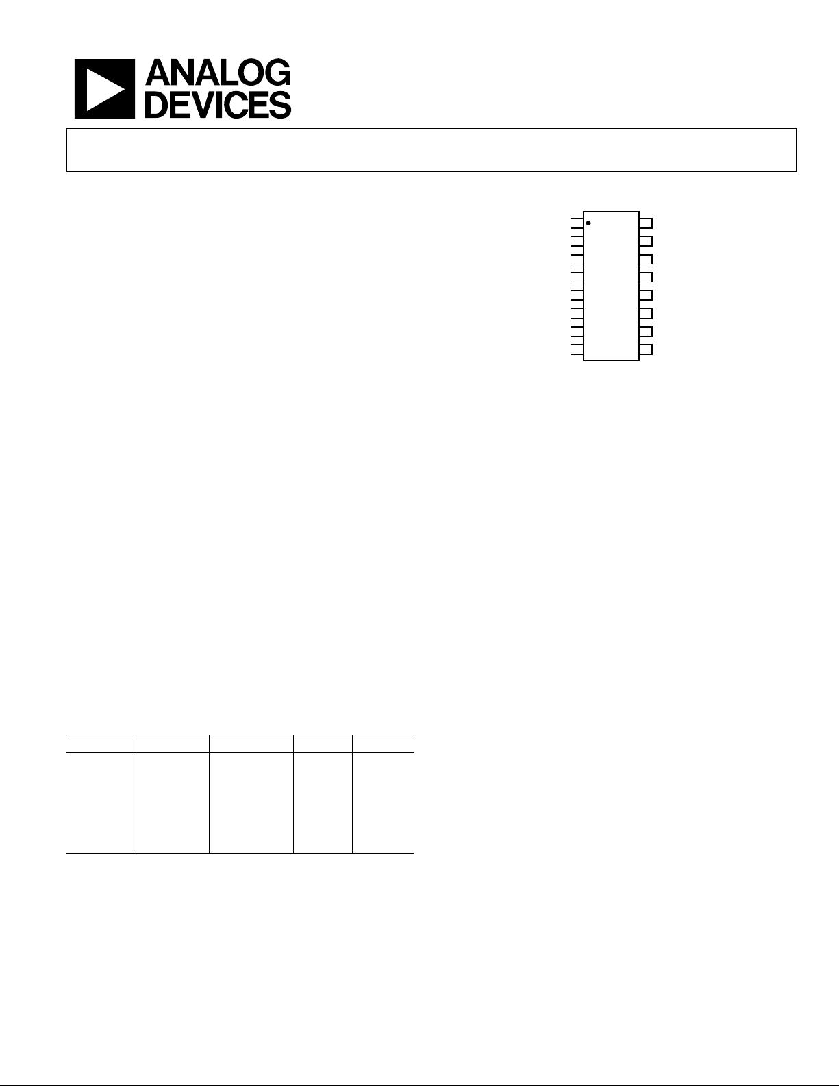
PIN CONFIGURATION
1
+IN A
2
+IN B
3
+IN C
4
+IN D OUT D
ADD8706
5
+IN E
6
V+
7
+IN F
89
–IN F OUT F
NC = NO CONNECT
Figure 1. 16-Lead TSSOP
16
15
14
13
12
11
10
OUT A
OUT B
OUT C
OUT E
V–
NC
04352-0-001
Rev. 0
Information furnished by Analog Devices is believed to be accurate and reliable.
However, no responsibility is assumed by Analog Devices for its use, nor for any
infringements of patents or other rights of third parties that may result from its use.
Specifications subject to change without notice. No license is granted by implication
or otherwise under any patent or patent rights of Analog Devices. Trademarks and
registered trademarks are the property of their respective owners.
One Technology Way, P.O. Box 9106, Norwood, MA 02062-9106, U.S.A.
Tel: 781.329.4700
Fax: 781.326.8703 © 2003 Analog Devices, Inc. All rights reserved.
www.analog.com
Page 2

ADD8706
TABLE OF CONTENTS
Electrical Characteristics ................................................................. 3
Absolute Maximum Ratings............................................................ 5
ESD Caution.................................................................................. 5
Typical Performance Characteristics ............................................. 6
Application Information.................................................................. 9
REVISION HISTORY
Revision 0: Initial Version
Theory.............................................................................................9
Input/Output Characteristics ......................................................9
Important Note..............................................................................9
Outline Dimensions....................................................................... 11
Ordering Guide .......................................................................... 11
Rev. 0 | Page 2 of 12
Page 3

ADD8706
ELECTRICAL CHARACTERISTICS
Table 2. VS = 16 V, VCM = VS/2, TA @ 25 °C, unless otherwise noted
Parameter Symbol Condition Min Typ Max Unit
SUPPLY CHARACTERISTICS
Supply Voltage V
S
Power Supply Rejection Ratio PSRR VS = 4 V to 17 V, –40°C ≤ TA ≤ +85°C 70 90 dB
Total Supply Current I
SY
–40°C ≤ TA ≤ +85°C 6 mA
INPUT CHARACTERISTICS
Offset Voltage V
OS
Offset Voltage Drift ∆VOS/∆T –40°C ≤ TA ≤ +85°C 10 µV/°C
Input Bias Current I
B
–40°C ≤ TA ≤ +85°C 1500 nA
Input Offset Current I
OS
Amplifier F –40°C ≤ TA ≤ +85°C 250 nA
Common-Mode Rejection Ratio CMRR –40°C ≤ TA ≤ +85°C
Amplifier F VCM = 0 to (VS – 1.7 V) 54 95 dB
Input Impedance Z
Input Capacitance C
IN
IN
OUTPUT CHARACTERISTICS
Output Voltage High (A) V
OH
Optimized for High Swing VIN = 16 V, IL = 5 mA 15.75 15.85 V
–40°C ≤ TA ≤ +85°C 15.65 V
Output Voltage High (B to D) V
OH
Optimized for Midrange VIN = 14 V, IL = 5 mA 13.90 13.985 V
–40°C ≤ TA ≤ +85°C 13.85 V
Output Voltage High (E) V
OH
Optimized for Low Swing VIN = 14 V, IL = 5 mA 13.9 13.99 V
–40°C ≤ TA ≤ +85°C 13.85 V
Output Voltage High (F) V
Optimized for V
COM
OH
V
–40°C ≤ TA ≤ +85°C 15.75 V
Output Voltage Low (A) V
OL
Optimized for High Swing VIN = 1.7 V, IL = 5 mA 1.71 1.730 V
–40°C ≤ TA ≤ +85°C 1.725 V
Output Voltage Low (B–D) V
OL
Optimized for Midrange VIN = 0 V, IL = 5 mA 200 300 mV
–40°C ≤ TA ≤ +85°C 350 mV
Output Voltage Low (E) V
OL
Optimized for Low Swing VIN = 0 V, IL = 5 mA 80 200 mV
Output Voltage Low (F) V
Optimized for V
COM
OL
V
–40°C ≤ TA ≤ +85°C 250 mV
Continuous Output Current (A to E) I
Continuous Output Current (F) I
Peak Output Current (A to E) I
Peak Output Current (F) I
OUT
OUT
PK
PK
4.5 16 V
VO = VS/2, No Load 4.5 5.4 mA
2 15 mV
400 1100 nA
10 100 nA
400 kΩ
1 pF
VIN = 16 V, IL = 100 µA 15.99 V
VIN = 14 V, IL = 100 µA 14 V
VIN = 14 V, IL = 100 µA 14 V
VIN = 16 V, IL = 100 µA 15.995 V
= 16 V, IL = 5 mA 15.8 15.9 V
IN
VIN = 1.7 V, IL = 100 µA 1.70 V
VIN = 0 V, IL = 100 µA 5 mV
VIN = 0 V, IL = 100 µA 5 mV
–40°C ≤ TA ≤ +85°C 300 mV
VIN = 0 V, IL = 100 µA 5 mV
= 0 V, IL = 5 mA 50 150 mV
IN
VS = 16 V 15 mA
VS = 16 V 35 mA
VS = 16 V 50 mA
VS = 16 V 200 mA
Rev. 0 | Page 3 of 12
Page 4

ADD8706
Parameter Symbol Condition Min Typ Max Unit
TRANSFER CHARACTERISTICS
Amplifier Gain A
Buffer Gain A
VO
VCL
–40°C ≤ TA ≤ +85°C 0.995 0.9980 1.005 V/V
Buffer Gain Linearity NL RL = 2kΩ, VO = 0.5 to (VS – 0.5 V) 0.01 %
DYNAMIC PERFORMANCE
Slew Rate SR RL = 2 kΩ, CL = 200 pF 4 6 V/µs
Bandwidth BW –3 dB, RL = 2 kΩ, CL = 40 pF 6 MHz
Phase Margin Øo RL = 2 kΩ, CL = 40 pF 55 Degrees
Channel Separation 75 dB
NOISE PERFORMANCE
Voltage Noise Density e
n
f = 10 kHz 25 nV/√Hz
Current Noise Density i
n
RL = 2 kΩ, VO = 0.5 to (VS – 2 V) 1 10 V/mV
RL = 2 kΩ 0.995 0.9985 1.005 V/V
f = 1 kHz 26 nV/√Hz
f = 10 kHz 0.8 pA/√Hz
Rev. 0 | Page 4 of 12
Page 5

ADD8706
ABSOLUTE MAXIMUM RATINGS
Table 3. ADD8706 Stress Ratings*
Parameter Rating
Supply Voltage (VS) 18 V
Input Voltage −0.5 V to VS + 0.5 V
Differential Input Voltage V
S
Storage Temperature Range –65°C to +150°C
Operating Temperature Range –40°C to +85°C
Junction Temperature Range –65°C to +150°C
Lead Temperature Range 300°C
ESD Tolerance (HBM) ±1500 V
*Stresses above those listed under Absolute Maximum Ratings
may cause permanent damage to the device. This is a stress
rating only; functional operation of the device at these or any
other conditions above those indicated in the operational
sections of this specification is not implied. Exposure to
absolute maximum rating conditions for extended periods may
affect device reliability.
ESD CAUTION
ESD (electrostatic discharge) sensitive device. Electrostatic charges as high as 4000 V readily
accumulate on the human body and test equipment and can discharge without detection. Although
this product features proprietary ESD protection circuitry, permanent damage may occur on devices
subjected to high energy electrostatic discharges. Therefore, proper ESD precautions are
recommended to avoid performance degradation or loss of functionality.
Table 4. Package Characteristics
Package Type θ
1
JA
θ
JC
Unit
16-Lead TSSOP (RU) 180 35 °C/W
1
θJA is specified for worst-case conditions, i.e., θJA is specified for devices
soldered onto a circuit board for surface-mount packages.
Rev. 0 | Page 5 of 12
Page 6

ADD8706
TYPICAL PERFORMANCE CHARACTERISTICS
70
60
50
40
30
20
QUANTITY OF AMPLIFIERS
10
0
–10–8–6–4–202468
INPUT OFFSET VOLTAGE (mV)
Figure 2. Input Offset Voltage, V
35
30
25
20
= 16 V
S
VS = 16V
VS = 16V
10
04532-0-025
INPUT OFFSET CURRENT (nA)
10k
100
18
16
14
12
10
8
6
4
2
0
–60 –40
–20 0 20 40 60 80 100
TEMPERATURE (°C)
Figure 5. Input Offset Current vs. Temperature
= 4.5V
V
S
SINK
1k
A
B, C, D
VS = 16V
F
04352-0-028
15
10
QUANTITY OF AMPLIFIERS
5
0
014
400
200
0
–200
–400
INPUT BIAS CURRENT (nA)
–600
–800
–60
28 42 56 70 84 98
TCVOS (µV/°C)
Figure 3. Input Offset Voltage Drift, V
= 16 V
S
A
E
B
F
D
C
–40–20020406080100
TEMPERATURE (°C)
VS = 16V
Figure 4. Input Bias Current vs. Temperature
04352-0-026
04352-0-027
10
∆OUTPUT VOLTAGE (mV)
1
0.1
0.001 100
0.01 0.1 1 10
LOAD CURRENT (mA)
E
Figure 6. Output Sink Voltage vs. Load Current, All Channels
10k
= 4.5V
=
V
S
SOURCE
1k
100
10
∆OUTPUT VOLTAGE (mV)
1
0.1
0.001 100
0.01 0.1 1 10
B, C, D, E
A
LOAD CURRENT (mA)
F
Figure 7. Output Source Voltage vs. Load Current, All Channels
04352-0-013
04352-0-015
Rev. 0 | Page 6 of 12
Page 7

ADD8706
10k
VS = 16V
SINK
1k
100
10
∆OUTPUT VOLTAGE (mV)
1
A
F
B, C, D
E
0.76
0.75
0.74
0.73
0.72
0.71
0.70
SUPPLY CURRENT/AMPLIFIER (mA)
VS = 16V
0.1
0.001 100
0.01 0.1 1 10
LOAD CURRENT (mA)
Figure 8. Output Sink Voltage vs. Load Current, All Channels
10k
VS = 16V
SOURCE
1k
100
10
∆OUTPUT VOLTAGE (mV)
1
0.1
0.001 100
A
0.01 0.1 1 10
B, C, D, E
F
LOAD CURRENT (mA)
Figure 9. Output Source Voltage vs. Load Current, All Channels
0.9
0.8
0.7
0.6
0.5
0.4
0.3
0.2
0.1
SUPPLY CURRENT PER AMPLIFIER (mA)
0
018264 8 10 12 14 16
SUPPLY VOLTAGE (V)
Figure 10. Supply Current vs. Supply Voltage
04352-0-014
04352-0-016
04352-0-022
0.69
–60
–40–200 20406080100
Figure 11. Supply Current vs. Temperature
120
VS = 16V
100
80
60
40
20
POWER SUPPLY REJECTION RATIO (dB)
0
100
140
VS = 16V
120
100
80
60
40
COMMON-MODE REJECTION (dB)
20
0
100
TEMPERATURE (°C)
–PSRR
+PSRR
1k 10k
FREQUENCY (Hz)
100k 1M 10M
Figure 12. PSRR v s. Frequency
1k 10k
FREQUENCY (Hz)
100k 1M 10M
Figure 13. CMRR vs. Fre quency
04352-0-029
04352-0-018
04352-0-010
Rev. 0 | Page 7 of 12
Page 8

ADD8706
100
80
60
40
GAIN (dB)
20
0
–20
1k 100M10k
100
VS = 16V
RL = 10kΩ
80
60
40
20
0
GAIN (dB)
–20
–40
–60
–80
–100
100k 100M1M
500
AV = 1
450
400
350
300
250
200
IMPEDANCE (Ω)
150
100
50
0
100
VS = 16V
R
CL = 40pF
100k 1M 10M
FREQUENCY (Hz)
Figure 14. Frequency vs. Gain and Sh ift
100pF
50pF
540pF
1040pF
FREQUENCY (Hz)
10M
Figure 15. Gain vs. Capacitive Load
1k 10k
FREQUENCY (Hz)
100k 1M 10M
Figure 16. Impedance vs. Frequency
= 10kΩ
L
CH. A–E
CH. F
0
45
90
135
180
225
PHASE SHIFT (Degrees)
04352-0-012
04352-0-008
04352-0-005
100
VS = ±16V
= 100mV
V
90
IN
AV = 1
= 10kΩ
R
80
L
70
60
50
40
OVERSHOOT (%)
30
20
10
0
10 1k100
CAPACITIVE LOAD (pF)
–OS
+OS
04352-0-020
Figure 17. Overshoot vs. Capacitive Load
=
VS = 16V
RL = 2kΩ
= 100pF
C
L
VOLTAGE (50mV/DIV)
TIME (1µs/DIV)
04352-0-021
Figure 18. Small-Signal Transient Response
VS = 16V
=
RL = 2kΩ
CL = 100pF
VOLTAGE (2V/DIV)
TIME (1µs/DIV)
04352-0-013
Figure 19. Large Signal Transient Response
Rev. 0 | Page 8 of 12
Page 9

ADD8706
APPLICATION INFORMATION
THEORY
The ADD8706 is designed for use in LCD gamma correction
circuits. This is an ideal on-chip solution for low-end panels. It
provides five gamma voltages and a V
output. These gamma
COM
voltages provide the reference voltages for the column driver
RDACs. Due to the capacitive nature of LCD panels, it is
necessary for these drivers to provide high capacitive load drive.
The V
pixels. The V
This requires the V
output is the center voltage common to all the LCD
COM
circuit is common to all the pixels in the panel.
COM
driver to supply continuous currents up
COM
to 35 mA.
INPUT/OUTPUT CHARACTERISTICS
The ADD8706 has five buffers specifically designed for the
needs of an LCD panel. Figure 20 shows a typical gamma
correction curve for a normally white twisted nematic LCD
panel. The symmetric curve comes from the need to reverse the
polarity on the LC pixels to avoid “burning” in the image.
Therefore, the application requires gamma voltages that come
close to both supply rails. To accommodate this transfer
function, the five ADD8706 buffers have been designed with
three different buffer designs in one package.
V
DD
V
G1
V
G2
V
G3
V
G4
V
G5
V
G6
V
G7
V
GAMMA VOLTAGE
G8
V
G9
V
G10
V
SS
016324864
Figure 20. LCD Gamma Correction Curve
The nature of LCD panels introduces a large amount of
parasitic capacitance from the column drivers as well as the
capacitance associated with the liquid crystals via the common
plane. This makes capacitive drive capability an important
factor when designing the gamma correction circuit.
GRAY SCALE BITS
04352-0-003
The outputs of the buffers and amplifier have been designed to
match the performance needs of the gamma correction and
circuits. All have rail-to-rail outputs, but the current drive
V
COM
capabilities differ. The difference in current drive and input
voltage range determine the buffer and amplifier use.
Buffer A has an NPN emitter-follower input stage, which
provides an input range that includes the top rail, but is limited
to 1.7 V away from the bottom rail. It is designed to source
15 mA of continuous current, making this buffer ideal for
providing the top voltage on the RDAC string.
Buffers B, C, and D use a single-supply PNP input stage with an
intermediate common-mode voltage range. The output was
designed to sink or source up to 15 mA of continuous current.
The limited input range and equivalent sink and source current
make these buffers suitable for the middle voltage ranges on the
RDAC string.
Buffer E also uses a single-supply PNP input stage, but the
output is designed to sink only up to 15 mA of continuous
current. This buffer is designed for the RDAC’s lower range.
Amplifier F is designed with an input range limited to midscale
applications. It is capable of delivering 35 mA of continuous
current. These qualities make Amplifier F suitable for V
COM
applications.
IMPORTANT NOTE
Because of the asymmetric nature of Buffers A and E, care must
be taken to connect an input that forces the amplifiers to
operate in their most productive output states. Buffer A has very
limited sink capabilities, while Buffer E does not source well. Set
the Buffer A input to enable the amplifier output to source
current and set the Buffer E input to force a sinking output
current. This means making sure the input is above the
midpoint of the common-mode input range for Buffer A and
below the midpoint for Buffer E. Mathematically speaking,
make sure V
Figure 21 shows an application using the ADD8706 to generate
10 gamma outputs. Note that the five outputs are routed
through another resistor network to generate the extra five
output voltages, which feed into the column driver.
> VS/2 for Buffer A and VIN < VS/2 for Buffer E.
IN
Rev. 0 | Page 9 of 12
Page 10

ADD8706
V
DD
V
DD
ADD8706
A
B
C
D
E
V
COM
F
V
COLUMN DRIVER
GAMMA 1
GAMMA 2
GAMMA 3
GAMMA 4
GAMMA 5
GAMMA 6
GAMMA 7
GAMMA 8
GAMMA 9
GAMMA 10
COM
Figure 21. ADD8706 Application Circuit
00000-x-000
Rev. 0 | Page 10 of 12
Page 11

ADD8706
OUTLINE DIMENSIONS
5.10
5.00
4.90
ORDERING GUIDE
1
Model
ADD8706ARUZ
ADD8706ARUZ-REEL
1
Z = Pb-free part.
Temperature Range Package Description Package Option
−40°C to +85°C
−40°C to +85°C
0.15
0.05
4.50
4.40
4.30
PIN 1
16
0.65
BSC
COPLANARITY
9
6.40
BSC
81
1.20 MAX
0.30
0.19
0.10
COMPLIANT TO JEDEC STANDARDS MO-153AB
SEATING
PLANE
0.20
0.09
8°
0°
Figure 22. 16-Lead Thin Shrink Small Outline Package [TSSOP] (RU)
Dimensions shown in millimeters
16-Lead TSSOP RU-16
16-Lead TSSOP RU-16
0.75
0.60
0.45
Rev. 0 | Page 11 of 12
Page 12

ADD8706
NOTES
© 2003 Analog Devices, Inc. All rights reserved. Trademarks and
registered trademarks are the property of their respective owners.
C04352–0–10/03(0)
Rev. 0 | Page 12 of 12
 Loading...