

Page 1
Dual Low Power 1.5% Comparator
A
V
www.BDTIC.com/ADI
FEATURES
400 mV ± 1.5% threshold
Supply range: 1.7 V to 5.5 V
Low quiescent current: 6.5 μA typical
Input range includes ground
Internal hysteresis: 8.9 mV typical
Low input bias current: ±10 nA maximum
Open-drain outputs
Supports wire-AND connections
Input polarities: one inverting and one noninverting
Low profile (1 mm) TSOT package
Drop-in replacement for the LT6700-1
APPLICATIONS
Li-Ion monitoring
Portable applications
Hand-held instruments
Window comparators
LED/relay driving
Optoisolator driving
Control systems
With 400 mV Reference
ADCMP670
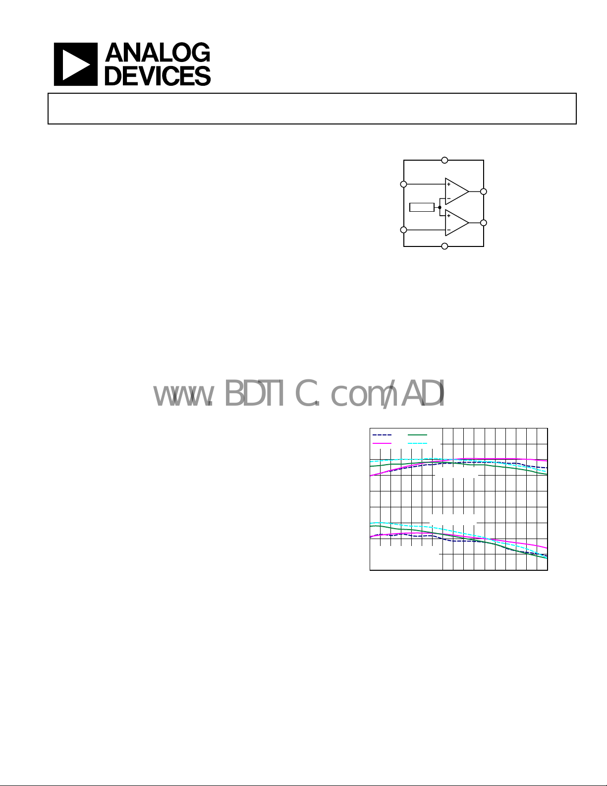
FUNCTIONAL BLOCK DIAGRAM
DD
ADCMP670-1
+IN
400mV
–INB
GND
Figure 1.
OUTA
OUTB
06493-001
GENERAL DESCRIPTION
The ADCMP670 consists of two low power, high accuracy,
comparator and reference circuits in a 6-lead TSOT package.
The internal 400 mV reference provides the ability to monitor
low voltage supplies. The device operates on a supply voltage
from 1.7 V to 5.5 V and draws only 6.5 μA typical, making it
suitable for low power system monitoring and portable applications. Hysteresis is included in the comparators. The comparator
outputs are open-drain and the output can be pulled up to any
voltage up to 5.5 V. The output stage is guaranteed to sink
greater than 5 mA over temperature.
The ADCMP670 is currently available in one model, the
CMP670-1. This model has one inverting input and one
AD
noninverting input, making it suitable for use as a window
comparator. The device is suitable for portable, commercial,
industrial, and automotive applications.
404
402
400
398
396
394
392
THRESHOLD VO LTAGE (mV)
390
388
386
1A
1B
TWO TYPICAL PARTS
COMP A AND COMP B
V
= 5V
DD
–40 –20 0 20 40 60 80 100 120
Figure 2. Comparator Thresholds vs. Temperature
2A
2B
RISING I NPUT
FALLING INPUT
TEMPERATURE (° C)
06493-002
Rev. 0
Information furnished by Analog Devices is believed to be accurate and reliable. However, no
responsibility is assumed by Anal og Devices for its use, nor for any infringements of patents or ot her
rights of third parties that may result from its use. Specifications subject to change without notice. No
license is granted by implication or otherwise under any patent or patent rights of Analog Devices.
Trademarks and registered trademarks are the property of their respective owners.
One Technology Way, P.O. Box 9106, Norwood, MA 02062-9106, U.S.A.
Tel: 781.329.4700 www.analog.com
Fax: 781.461.3113 ©2007 Analog Devices, Inc. All rights reserved.
Page 2

ADCMP670
www.BDTIC.com/ADI
TABLE OF CONTENTS
Features.............................................................................................. 1
Applications....................................................................................... 1
Functional Block Diagram .............................................................. 1
General Description ......................................................................... 1
Revision History ............................................................................... 2
Specifications..................................................................................... 3
Absolute Maximum Ratings............................................................ 6
Thermal Resistance ...................................................................... 6
ESD Caution.................................................................................. 6
Pin Configuration and Function Descriptions............................. 7
REVISION HISTORY
2/07—Revision 0: Initial Version
Typical Performance Characteristics..............................................8
Application Information................................................................ 13
Comparators and Internal Reference ...................................... 13
Power Supply............................................................................... 13
Inputs........................................................................................... 13
Outputs........................................................................................ 13
Adding Hysteresis....................................................................... 13
Outline Dimensions....................................................................... 14
Ordering Guide .......................................................................... 14
Rev. 0 | Page 2 of 16
Page 3

ADCMP670
www.BDTIC.com/ADI
SPECIFICATIONS
VDD = 1.7 V to 5.5 V, TA = 25°C, unless otherwise noted.
Table 1.
Parameter Min Typ Max Unit Test Conditions/Comments
THRESHOLDS
Rising Input Threshold Voltage 394 400 406 mV VDD = 1.7 V
395 400 405 mV VDD = 5.5 V
Falling Input Threshold Voltage 386 391.1 401 mV VDD = 1.7 V
387 391.1 400 mV VDD = 5.5 V
Hysteresis = V
INPUT CHARACTERISTICS
Input Bias Current 0.01 10 nA VDD = 1.7 V, VIN = VDD
4 10 nA VDD = 1.7 V, VIN = 0.1 V
OPEN-DRAN OUTPUTS
Output Low Voltage
130 200 mV VDD = 5.5 V, I
Output Leakage Current
0.01 0.8 μA VDD =1.7 V, V
DYNAMIC PERFORMANCE
High-to-Low Propagation Delay 10 μs VDD = 5.5 V, VOL = 400 mV
Low-to-High Propagation Delay 8 μs VDD = 5.5 V, VOH = 0.9 × VDD
Output Rise Time 0.5 μs VDD = 5.5 V, VO = (0.1 to 0.9) × VDD
Output Fall Time 0.07 μs VDD = 5.5 V, VO = (0.1 to 0.9) × VDD
POWER SUPPLY
Supply Current
6.5 11 μA VDD = 5.5 V
1
RL = 100 kΩ, VO = 2 V swing.
2
10 mV input overdrive.
3
VIN = 40 mV overdrive.
4
RL = 10 kΩ.
5
No load current.
1
– V
TH(R)
5
7 8.9 11 mV
TH(F)
2
3
2, 4
140 200 mV VDD = 1.7 V, I
0.01 0.8 μA VDD =1.7 V, V
5.7 10 μA VDD = 1.7 V
= 3 mA
OUT
= 5 mA
OUT
= VDD
OUT
= 5.5 V
OUT
Rev. 0 | Page 3 of 16
Page 4
ADCMP670
www.BDTIC.com/ADI
VDD = 1.7 V to 5.5 V, 0°C ≤ TA ≤ 70°C, unless otherwise noted.
Table 2.
Parameter Min Typ Max Unit Test Conditions/Comments
THRESHOLDS
Rising Input Threshold Voltage 391 409 mV VDD = 1.7 V
392.5 407.5 mV VDD = 5.5 V
Falling Input Threshold Voltage 383.5 403.5 mV VDD = 1.7 V
384.5 402.5 mV VDD = 5.5 V
Hysteresis = V
INPUT CHARACTERISTICS
Input Bias Current 15 nA VDD = 1.7 V, VIN = VDD
15 nA VDD = 1.7 V, VIN = 0.1 V
OPEN-DRAIN OUTPUTS
Output Low Voltage
250 mV VDD = 5.5 V, I
Output Leakage Current
1 μA VDD =1.7 V, V
POWER SUPPLY
Supply Current
14 μA VDD = 5.5 V
1
RL = 100 kΩ, VO = 2 V swing.
2
10 mV input overdrive.
3
VIN = 40 mV overdrive.
4
No load.
V
= 1.7 V to 5.5 V, −40°C ≤ TA ≤ 85°C, unless otherwise noted.
DD
1
– V
TH(R)
4
6.5 12.5 mV
TH(F)
2
3
250 mV VDD = 1.7 V, I
1 μA VDD =1.7 V, V
13 μA VDD = 1.7 V
= 3 mA
OUT
= 5 mA
OUT
= VDD
OUT
= 5.5 V
OUT
Table 3.
Parameter Min Typ Max Unit Test Conditions/Comments
THRESHOLDS
1
Rising Input Threshold Voltage 390 410 mV VDD = 1.7 V
392 408 mV VDD = 5.5 V
Falling Input Threshold Voltage 382.5 404.5 mV VDD = 1.7 V
383.5 403.5 mV VDD = 5.5 V
Hysteresis = V
TH(R)
– V
5.5 13.0 mV
TH(F)
INPUT CHARACTERISTICS
Input Bias Current 15 nA VDD = 1.7 V, VIN = VDD
15 nA VDD = 1.7 V, VIN = 0.1 V
OPEN-DRAIN OUTPUTS
Output Low Voltage
250 mV VDD = 5.5 V, I
Output Leakage Current
1 μA VDD =1.7 V, V
2
3
250 mV VDD = 1.7 V, I
1 μA VDD =1.7 V, V
= 3 mA
OUT
= 5 mA
OUT
= VDD
OUT
= 5.5 V
OUT
POWER SUPPLY
Supply Current
4
14 μA VDD = 1.7 V
15 μA VDD = 5.5 V
1
RL = 100 kΩ, VO = 2 V swing.
2
10 mV input overdrive.
3
VIN = 40 mV overdrive.
4
No load.
Rev. 0 | Page 4 of 16
Page 5

ADCMP670
www.BDTIC.com/ADI
VDD = 1.7 V to 5.5 V, −40°C ≤ TA ≤ 125°C, unless otherwise noted.
Table 4.
Parameter Min Typ Max Unit Test Conditions/Comments
THRESHOLDS
Rising Input Threshold Voltage 390 411 mV VDD = 1.7 V
392 410 mV VDD = 5.5 V
Falling Input Threshold Voltage 381.5 405.5 mV VDD = 1.7 V
381.05 404.5 mV VDD = 5.5 V
Hysteresis = V
INPUT CHARACTERISTICS
Input Bias Current 45 nA VDD = 1.7 V, VIN = VDD
45 nA VDD = 1.7 V, VIN = 0.1 V
OPEN-DRAIN OUTPUTS
Output Low Voltage
250 mV VDD = 5.5 V, I
Output Leakage Current
1 μA VDD = 1.7 V, V
POWER SUPPLY
Supply Current
17 μA VDD= 5.5 V
1
RL = 100 kΩ, VO = 2 V swing.
2
10 mV input overdrive.
3
VIN = 40 mV overdrive.
4
No load.
1
– V
TH(R)
4
2 13.5 mV
TH(F)
2
3
250 mV VDD = 1.7 V, I
1 μA VDD = 1.7 V, V
16 μA VDD = 1.7 V
= 3 mA
OUT
= 5 mA
OUT
OUT
OUT
= VDD
= 5.5 V
Rev. 0 | Page 5 of 16
Page 6

ADCMP670
www.BDTIC.com/ADI
ABSOLUTE MAXIMUM RATINGS
Table 5.
Parameter Range
VDD −0.3 V to +6 V
+INA, −INB −0.3 V to +6 V
OUTA, OUTB −0.3 V to +6 V
Output Short Circuit Duration1 Indefinite
Input Current −10 mA
Operating Temperature Range −40°C to +125°C
Storage Temperature Range −65°C to +150°C
Lead Temperature
Soldering (10 sec) 300°C
Vapor Phase (60 sec) 215°C
Infrared (15 sec) 220°C
1
When the output is shorted indefinitely, the use of a heat sink may be requir ed to
keep the junction temperature within the absolute maximum ratings.
Stresses above those listed under Absolute Maximum Ratings
y cause permanent damage to the device. This is a stress
ma
rating only; functional operation of the device at these or any
other conditions above those indicated in the operational
section of this specification is not implied. Exposure to absolute
maximum rating conditions for extended periods may affect
device reliability.
THERMAL RESISTANCE
θJA is specified for the worst-case conditions, that is, a device
soldered in a circuit board for surface-mount packages.
Table 6. Thermal Resistance
Package Type θ
6-Lead TSOT 200 °C/W
Unit
JA
ESD CAUTION
Rev. 0 | Page 6 of 16
Page 7

ADCMP670
www.BDTIC.com/ADI
PIN CONFIGURATION AND FUNCTION DESCRIPTIONS
1
OUTA
2
GND
3
+INA
Figure 3. Pin Configuration
Table 7. Pin Function Descriptions
Pin No. Mnemonic Description
1 OUTA Open-Drain Output for Comparator A.
2 GND Ground.
3 +INA
Monitors analog input voltage on Comparator A. Connected to noninverting input. The other input of Comparator A is
connected to a 400 mV reference.
4 −INB
Monitors analog input voltage on Comparator B. Connected to inverting input. The other input of Comparator B is
connected to a 400 mV reference.
5 V
Power Supply Pin.
DD
6 OUTB Open-Drain Output for Comparator B.
ADCMP670-1
TOP VIEW
(Not to Scal e)
6
OUTB
5
V
DD
4
–INB
06493-003
Rev. 0 | Page 7 of 16
Page 8

ADCMP670
www.BDTIC.com/ADI
TYPICAL PERFORMANCE CHARACTERISTICS
60
50
VDD = 5V
= 25°C
T
A
50
40
VDD = 5V
= 25°C
T
A
40
30
20
PERCENT OF UNI TS (%)
10
0
394 395 396 397 398 399 400 401 402 403 404 405 406
RISING INPUT THRESHOL D VOLTAG E (mV)
06493-004
30
20
PERCENT OF UNI TS (%)
10
0
388 389 390 391 392 393 394 395 396 397 398 399 400
FALLING INPUT THRESHOLD VOLTAGE (mV)
Figure 4. Distribution of Rising Input Threshold Voltage Figure 7. Distribution of Falling Input Threshold Voltage
35
VDD = 5V
= 25°C
T
A
30
25
20
15
10
PERCENT OF UNI TS (%)
5
0
6.0 6.4 6.8 7.2 7.6 8. 0 8.4 8.8 9.2 9.6 10.0 10. 4 10.8
HYSTERESIS (mV)
06493-005
402
401
400
399
RISING INPUT THRESHOLD VOLTAGE (mV)
398
VDD = 1.8V
VDD = 2.5V
VDD = 3.3V
VDD = 5.0V
–40 –20 1200 20406080100
TEMPERATURE (° C)
Figure 5. Distribution of Hysteresis Figure 8. Rising Input Threshold Voltage vs. Temperature
06493-007
06493-008
404
402
400
398
RISING INPUT THRESHOLD VOLTAGE (mV)
396
1
2
3
4
–40 –20 1200 20406080100
TEMPERATURE (° C)
FOUR TYPI CAL PARTS
= 5V
V
DD
06493-006
Figure 6. Rising Input Threshold Voltage vs. Temperature
Rev. 0 | Page 8 of 16
401
TA = –40°C
400
= +25°C
T
A
T
= +85°C
A
T
= +125°C
A
SUPPLY VOLTAGE (V)
RISING INPUT THRESHOLD VOLTAGE (mV)
399
398
397
396
395
1.7 5.75.24.74.23.73.22.72.2
Figure 9. Rising Input Threshold Voltage vs. Supply Voltage
06493-009
Page 9

ADCMP670
www.BDTIC.com/ADI
12.0
11.5
11.0
10.5
10.0
9.5
9.0
8.5
8.0
7.5
7.0
HYSTERESIS (mV)
6.5
6.0
5.5
5.0
4.5
4.0
1A
1B
2A
2B
FOUR TYPI CAL PARTS
V
= 5V
DD
–40 –20 1200 20406080100
TEMPERATURE (° C)
Figure 10. Hysteresis vs. Temperature Figure 13. Hysteresis vs. Temperature
06493-010
12.0
11.5
11.0
10.5
10.0
9.5
9.0
8.5
8.0
7.5
7.0
HYSTERESIS (mV)
6.5
6.0
5.5
5.0
4.5
4.0
VDD = 1.8V
VDD = 2.5V
VDD = 3.3V
VDD = 5.0V
–40 –20 1200 20406080100
TEMPERATURE (°C)
06493-013
HYSTERESIS (mV)
12
11
10
9
8
7
6
5
4
1.7 5.75.24. 74.23.73.22.72.2
SUPPLY VOLTAGE (V)
TA = +125°C
T
= +25°C
A
= +85°C
T
A
= –40°C
T
A
Figure 11. Hysteresis vs. Supply Voltage Figure 14. Minimum Supply Voltage
10
NO LOAD CURRENT
9
8
T
= +85°C
A
7
6
SUPPLY CURRENT (mA)
5
4
1.7 2.2 2.7 3.2 3.7 4.2 4.7
= –40°C
T
A
SUPPLY VOLTAGE (V)
TA = +125°C
= +25°C
T
A
Figure 12. Quiescent Supply Current vs. Supply Voltage
5.2
1
0
–1
–2
–3
THRESHOLD SHIFT (mV)
–4
–5
1.5 2.52.42.32.22. 12.01.91. 81.71.6
06493-011
50
40
30
20
SUPPLY CURRENT (µA)
10
0
00.51.0
06493-012
SUPPLY VOLTAGE (V)
= +85°C
T
A
TA = +125°C
SUPPLY VOLTAGE (V)
= +25°C
T
A
TA = –40°C
TA = +25°C
TA = +85°C
TA = +125°C
T
= –40°C
A
1.5
Figure 15. Start-Up Supply Current
06493-014
06493-015
Rev. 0 | Page 9 of 16
Page 10

ADCMP670
www.BDTIC.com/ADI
1000
TA = –40°C
VDD = 5.0V
VDD = 3.3V
VDD = 2.5V
VDD = 1.7V
1000
TA = 25°C
VDD = 5.0V
VDD = 3.3V
VDD = 2.5V
VDD = 1.7V
100
10
SUPPLY CURRENT ( µ A)
1
0.001 1001010.10.01
OUTPUT SI NK CURRE NT (mA)
Figure 16. Supply Current vs. Output Sink Current
1000
TA = 85°C
100
10
SUPPLY CURRENT ( µ A)
VDD = 5.0V
VDD = 3.3V
VDD = 2.5V
VDD = 1.7V
100
10
SUPPLY CURRENT ( µ A)
1
0.001 1001010.10.01
06493-016
OUTPUT SI NK CURRE NT (mA)
06493-017
Figure 19. Supply Current vs. Output Sink Current
10k
TA = +125°C
1k
100
= +85°C
T
T
= –40°C
A
A
T
= +25°C
A
10
INPUT BIAS CURRENT (nA)
1
CURRENT IS GO ING
OUT OF THE DEVICE.
V
= 5V
DD
–0.3V < V
IB
< 0V
1
0.001 1001010.10.01
OUTPUT SI NK CURRE NT (mA)
Figure 17. Supply Current vs. Output Sink Current
3
1
–1
–3
INPUT BIAS CURRENT (nA)
–5
CURRENT IS POS ITIVE
GOING INTO THE DEVICE.
V
= 5V
DD
0V < V
< 1V
–7
IB
00.2 0.6
0.4 0.8
INPUT VOLTAGE (V)
Figure 18. Low Level Inpu t Bias Cur rent
TA = +125°C
TA = +85°C
TA = +25°C
TA = –40°C
1.0
0.1
–0.3 –0.2 –0.1
06493-018
INPUT VOLTAGE (V)
0
06493-019
Figure 20. Below Ground Input Bias Current
10
TA = +125°C
1
TA = +85°C
= 5V
> 1V
TA = +25°C
INPUT VOLTAGE (V)
0.1
INPUT BIAS CURRENT (nA)
CURRENT IS GO ING INTO THE DEVICE
V
DD
V
IB
0.01
12 4
06493-020
TA = –40°C
3
5
06493-021
Figure 21. High Level Input Bias Current
Rev. 0 | Page 10 of 16
Page 11

ADCMP670
www.BDTIC.com/ADI
1000
100
TA = 25°C
VDD = 5.0V
VDD = 3.3V
VDD = 2.5V
VDD = 1.8V
1000
100
= –40°C
T
A
VDD = 5.0V
VDD = 3.3V
VDD = 2.5V
VDD = 1.8V
10
OUTPUT SATURATION VOLTAGE (mV)
1
0.001 0. 10.01
OUTPUT SI NK CURRENT (mA)
101
06493-022
10
OUTPUT SATURATION VOLTAGE (mV)
1
0.001 0.1
OUTPUT SI NK CURRENT (mA)
100.01 1
Figure 22. Output Saturation Voltage vs. Output Sink Current Figure 25. Output Saturation Voltage vs. Output Sink Current
1000
TA = 85°C
VDD = 5.0V
VDD = 3.3V
VDD = 2.5V
VDD = 1.8V
100
10
OUTPUT SATURATION VOLTAGE (mV)
1
0.001 0.1
OUTPUT SI NK CURRENT (mA)
SHORT-CIRCUIT CURRENT (mA)
100.01 1
06493-024
= 5V
V
DD
70
60
50
40
30
20
10
0
02804
T
= +25°C
A
= +85°C
T
A
OUTPUT VO LTAGE (V )
T
= –40°C
A
TA = +125°C
Figure 23. Output Saturation Voltage vs. Output Sink Current Figure 26. Output Short-Circuit Current
06493-023
06493-025
TA = 25°C
60
50
40
30
20
SHORT-CIRCUIT CURRENT (mA)
10
0
02704
OUTPUT VOLTAGE (V)
Figure 24. Output Short-Circuit Current Figure 27. Output Leakage Current
VDD = 5.0V
= 3.3V
V
DD
V
= 2.5V
DD
V
= 1.8V
DD
VDD = 5V
TA = +125°C
1
T
= +85°C
A
T
= +25°C
0.1
0.01
OUTPUT LEAKAGE CURRENT (nA)
0.001
01231045
06493-026
OUTPUT VOLTAGE (V)
A
T
= –40°C
A
Rev. 0 | Page 11 of 16
06493-027
Page 12

ADCMP670
www.BDTIC.com/ADI
60
TA = 25°C
50
40
30
20
PROPAGATION DELAY (µs)
10
LH NONINV
LH INV
HL NONINV
HL INV
100
VDD = 5V
C
= 20pF
L
T
= 25°C
A
10
RISE
1
0.1
RISE AND FALL TIMES (µ s)
FALL
0
0 204060
INPUT OVERDRI VE (mV)
80 100
Figure 28. Propagation Delay vs. Input Overdrive Figure 30. Rise and Fa
NON INV (OUTA)
2
INV (OUTB)
3
VIN (+INA, –INB)
1
CH1 50.0mV
CH3 5.00V
CH2 5.00V M20.0µs CH1 7mV
Figure 29. Noninverting and Inverting Comparators Propagation Delay
0.01
0.1 1
06493-028
OUTPUT PULL-UP RESISTOR (kΩ)
10
100 1000
ll Times vs. Output Pull-Up Resistor
06493-029
06493-030
Rev. 0 | Page 12 of 16
Page 13

ADCMP670
www.BDTIC.com/ADI
APPLICATION INFORMATION
The ADCMP670 is a dual low power comparator with a
built-in 400 mV reference that operates from 1.7 V to 5.5 V.
The comparator is 1.5% accurate with a built-in hysteresis of
8.9 mV. The outputs are open-drain, capable of sinking 40 mA.
COMPARATORS AND INTERNAL REFERENCE
Each comparator has one input available externally.
Comparator A has a noninverting input and Comparator B has
an inverting input available. The other comparator inputs are
connected internally to the 400 mV reference. The rising input
threshold voltage of the comparators is designed to be equal to
that of the reference.
POWER SUPPLY
The ADCMP670 is designed to operate from 1.7 V to 5.5 V.
A 0.1 μF decoupling capacitor is recommended between V
and GND.
DD
INPUTS
The comparator inputs are limited to the maximum VDD voltage
range. The voltage on these inputs can be above V
above the maximum allowed V
resistor string to the input, care must be taken when choosing
resistor values. This is due to the fact that the input bias current
will be in parallel with the bottom resistor of the string. This
bottom resistor must therefore be chosen first to control the
error introduced by this bias current.
voltage. When adding a
DD
but never
DD
OUTPUTS
The comparator outputs are open-drain and are also limited to
the maximum specified V
voltage. These outputs are capable of sinking up to 40 mA.
Outputs can be tied together to provide a window comparator
with a single output.
voltage range, regardless of the VDD
DD
ADDING HYSTERESIS
To prevent oscillations at the output caused by noise or
slowly moving signals passing the switching threshold, each
comparator has built-in hysteresis of approximately 8.9 mV.
Positive feedback can be used to increase hysteresis to the
noninverting comparator.
Rev. 0 | Page 13 of 16
Page 14

ADCMP670
www.BDTIC.com/ADI
OUTLINE DIMENSIONS
2.90 BSC
4526
1.60 BSC
13
PIN 1
INDICATOR
*
0.90
0.87
0.84
0.10 MAX
*
COMPLIANT TO JEDEC STANDARDS MO-193-AA WITH
THE EXCEPTION OF PACKAGE HEIGHT AND THICKNESS.
1.90
BSC
0.50
0.30
Figure 31. 6-Lead Thin Small Outline Transistor Package [TSOT]
Dim
ensions shown in millimeters
ORDERING GUIDE
Model Temperature Range Package Description Package Option Branding
ADCMP670-1YUJZ-RL7 –40°C to +125°C 6-Lead Thin Small Outline Transistor Package [TSOT] UJ-6 M97
1
Z = Pb-free part.
1
2.80 BSC
0.95 BSC
*
1.00 MAX
SEATING
PLANE
(UJ-6)
0.20
0.08
8°
0.60
4°
0.45
0°
0.30
Rev. 0 | Page 14 of 16
Page 15

ADCMP670
www.BDTIC.com/ADI
NOTES
Rev. 0 | Page 15 of 16
Page 16

ADCMP670
www.BDTIC.com/ADI
NOTES
©2007 Analog Devices, Inc. All rights reserved. Trademarks and
registered trademarks are the property of their respective owners.
D06493-0-2/07(0)
Rev. 0 | Page 16 of 16
 Loading...