

Page 1
Two Selectable Inputs, 12 LVPECL Outputs,
FEATURES FEATURES
2 selectable differential inputs 2 selectable differential inputs
4.8 GHz operating frequency 4.8 GHz operating frequency
75 fs rms broadband random jitter 75 fs rms broadband random jitter
On-chip input terminations On-chip input terminations
3.3 V power supply 3.3 V power supply
APPLICATIONS APPLICATIONS
Low jitter clock distribution Low jitter clock distribution
Clock and data signal restoration Clock and data signal restoration
Level translation Level translation
Wireless communications Wireless communications
Wired communications Wired communications
Medical and industrial imaging Medical and industrial imaging
ATE and high performance instrumentation ATE and high performance instrumentation
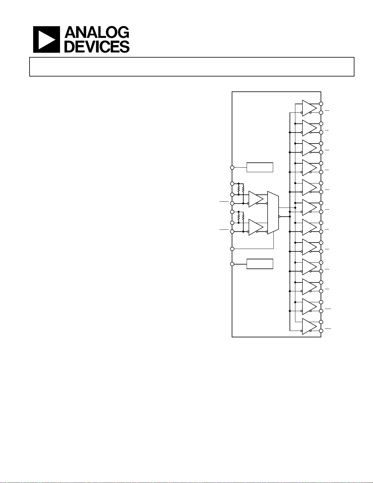
GENERAL DESCRIPTION GENERAL DESCRIPTION
The ADCLK954 is an ultrafast clock fanout buffer fabricated on
The ADCLK954 is an ultrafast clock fanout buffer fabricated on
the Analog Devices, Inc., proprietary XFCB3 silicon germa-
the Analog Devices, Inc., proprietary XFCB3 silicon germanium (SiGe) bipolar process. This device is designed for high
nium (SiGe) bipolar process. This device is designed for high
speed applications requiring low jitter.
speed applications requiring low jitter.
The device has two selectable differential inputs via the IN_SEL
The device has two selectable differential inputs via the IN_SEL
control pin. Both inputs are equipped with center tapped,
control pin. Both inputs are equipped with center tapped,
differential, 100 Ω on-chip termination resistors. The inputs
differential, 100 Ω on-chip termination resistors. The inputs
accept dc-coupled LVPECL, CML, 3.3 V CMOS (single-ended),
accept dc-coupled LVPECL, CML, 3.3 V CMOS (single-ended),
and ac-coupled 1.8 V CMOS, LVDS, and LVPECL inputs. A
and ac-coupled 1.8 V CMOS, LVDS, and LVPECL inputs. A
V
V
x pin is available for biasing ac-coupled inputs.
x pin is available for biasing ac-coupled inputs.
REF
REF
The ADCLK954 features 12 full-swing emitter coupled logic
The ADCLK954 features 12 full-swing emitter coupled logic
(ECL) output drivers. For LVPECL (positive ECL) operation,
(ECL) output drivers. For LVPECL (positive ECL) operation,
bias V
bias V
to the positive supply and VEE to ground. For ECL
to the positive supply and VEE to ground. For ECL
CC
CC
operation, bias V
operation, bias V
The output stages are designed to directly drive 800 mV each
The output stages are designed to directly drive 800 mV each
side into 50 Ω terminated to VCC − 2 V for a total differential
side into 50 Ω terminated to V
output swing of 1.6 V.
output swing of 1.6 V.
The ADCLK954 is available in a 40-lead LFCSP and specified
The ADCLK954 is available in a 40-lead LFCSP and specified
for operation over the standard industrial temperature range of
for operation over the standard industrial temperature range of
−40°C to +85°C.
−40°C to +85°C.
to ground and VEE to the negative supply.
to ground and VEE to the negative supply.
CC
CC
− 2 V for a total differential
CC
SiGe Clock Fanout Buffer
ADCLK954
FUNCTIONAL BLOCK DIAGRAM FUNCTIONAL BLOCK DIAGRAM
ADCLK954
V
REF
VT0
CLK0
CLK0
VT1
CLK1
CLK1
IN_SEL
V
REF
0
1
REFERENCE
REFERENCE
Figure 1.
LVPECL
Q0
Q0
Q1
Q1
Q2
Q2
Q3
Q3
Q4
Q4
Q5
Q5
Q6
Q6
Q7
Q7
Q8
Q8
Q9
Q9
Q10
Q10
Q11
Q11
07968-001
Rev. B
Information furnished by Analog Devices is believed to be accurate and reliable. However, no
responsibility is assumed by Analog Devices for its use, nor for any infringements of patents or other
rights of third parties that may result from its use. Specifications subject to change without notice. No
license is granted by implication or otherwise under any patent or patent rights of Analog Devices.
Trademarks and registered trademarks are the property of their respective owners.
One Technology Way, P.O. Box 9106, Norwood, MA 02062-9106, U.S.A.
Tel: 781.329.4700 www.analog.com
Fax: 781.461.3113 ©2009–2010 Analog Devices, Inc. All rights reserved.
Page 2

ADCLK954
TABLE OF CONTENTS
Features .............................................................................................. 1
Applications ....................................................................................... 1
General Description ......................................................................... 1
Functional Block Diagram .............................................................. 1
Revision History ............................................................................... 2
Specifications ..................................................................................... 3
Electrical Characteristics ............................................................. 3
Absolute Maximum Ratings ............................................................ 5
Determining Junction Temperature .......................................... 5
ESD Caution .................................................................................. 5
Thermal Performance .................................................................. 5
REVISION HISTORY
6/10—Rev. A to Rev. B
Changed Output Voltage Differential Parameter to Output
Voltage, Single Ended Parameter, Table 1 ..................................... 3
Changes to Output Voltage, Single Ended Parameter, Table 1 ... 3
7/09—Rev. 0 to Rev. A
Changes to Table 1 ............................................................................ 3
Changes to Negative Supply Current, Table 4 ............................... 4
Changes to Positive Supply Current, Table 4 ................................ 4
Changes to Figure 10 ........................................................................ 8
1/09—Revision 0: Initial Version
Pin Configuration and Function Descriptions ..............................6
Typical Performance Characteristics ..............................................7
Functional Description .....................................................................9
Clock Inputs ...................................................................................9
Clock Outputs ................................................................................9
Clock Input Select (IN_SEL) Settings...................................... 10
PCB Layout Considerations ...................................................... 10
Input Termination Options ....................................................... 11
Outline Dimensions ....................................................................... 12
Ordering Guide .......................................................................... 12
Rev. B | Page 2 of 12
Page 3
ADCLK954
SPECIFICATIONS
ELECTRICAL CHARACTERISTICS
Typical (Typ column) values are given for VCC − VEE = 3.3 V and TA = 25°C, unless otherwise noted. Minimum (Min column) and maximum
(Max column) values are given over the full V
Table 1. Clock Inputs and Outputs
Parameter Symbol Min Typ Max Unit Test Conditions/Comments
DC INPUT CHARACTERISTICS
Input Common-Mode Voltage V
VEE + 1.5 VCC − 0.1 V
ICM
Input Differential Range VID 0.4 3.4 V p-p ±1.7 V between input pins
Input Capacitance CIN 0.4 pF
Input Resistance
Single-Ended Mode 50 Ω
Differential Mode 100 Ω
Common Mode 50 kΩ Open VTx
Input Bias Current 20 µA
Hysteresis 10 mV
DC OUTPUT CHARACTERISTICS
Output Voltage High Level VOH V
Output Voltage Low Level VOL V
Output Voltage, Single Ended VO 610 960 mV VOH − VOL, output static
Reference Voltage V
REF
Output Voltage (VCC + 1)/2 V −500 µA to +500 µA
Output Resistance 235 Ω
− VEE = 3.3 V ± 10% and TA = −40°C to +85°C variation, unless otherwise noted.
CC
− 1.26 VCC − 0.76 V 50 Ω to (VCC − 2.0 V)
CC
− 1.99 VCC − 1.54 V 50 Ω to (VCC − 2.0 V)
CC
Table 2. Timing Characteristics
Parameter Symbol Min Typ Max Unit Test Conditions/Comments
AC PERFORMANCE
Maximum Output Frequency 4.5 4.8 GHz
See Figure 4 for differential output voltage vs.
frequency, > 0.8 V differential output swing
Output Rise Time tR 40 75 90 ps 20% to 80% measured differentially
Output Fall Time tF 40 75 90 ps
Propagation Delay tPD 175 210 245 ps V
= 2 V, VID = 1.6 V p-p
ICM
Temperature Coefficient 50 fs/°C
Output-to-Output Skew
1
9 25 ps
Part-to-Part Skew 45 ps VID = 1.6 V p-p
Additive Time Jitter
Integrated Random Jitter 28 fs rms BW = 12 kHz − 20 MHz, CLK = 1 GHz
Broadband Random Jitter2 75 fs rms VID = 1.6 V p-p, 8 V/ns, V
Crosstalk-Induced Jitter
3
90 fs rms
ICM
= 2 V
CLOCK OUTPUT PHASE NOISE
Absolute Phase Noise
Input slew rate > 1 V/ns (see Figure 11, the
phase noise plot, for more details)
fIN = 1 GHz −119 dBc/Hz @100 Hz offset
−134 dBc/Hz @1 kHz offset
−145 dBc/Hz @10 kHz offset
−150 dBc/Hz @100 kHz offset
−150 dBc/Hz >1 MHz offset
1
The output skew is the difference between any two similar delay paths while operating at the same voltage and temperature.
2
Measured at the rising edge of the clock signal; calculated using the SNR of the ADC method.
3
This is the amount of added jitter measured at the output while two related, asynchronous, differential frequencies are applied to the inputs.
Rev. B | Page 3 of 12
Page 4
ADCLK954
Table 3. Input Select Control Pin
Parameter Symbol Min Typ Max Unit
Logic 1 Voltage VIH V
Logic 0 Voltage VIL V
Logic 1 Current IIH 100 A
Logic 0 Current IIL 0.6 mA
Capacitance 2 pF
Table 4. Power
Parameter Symbol Min Typ Max Unit Test Conditions/Comments
POWER SUPPLY
Supply Voltage Requirement VCC − VEE 2.97 3.63 V 3.3 V + 10%
Power Supply Current Static
Negative Supply Current I
Positive Supply Current I
Power Supply Rejection
Output Swing Supply Rejection
1
Change in tPD per change in VCC.
2
Change in output swing per change in VCC.
1
2
118 160 mA VCC − VEE = 3.3 V ± 10%
VEE
406 460 mA VCC − VEE = 3.3 V ± 10%
VCC
PSR
<3 ps/V VCC − VEE = 3.3 V ± 10%
VCC
PSR
28 dB VCC − VEE = 3.3 V ± 10%
VCC
− 0.4 VCC V
CC
1.0 V
EE
Rev. B | Page 4 of 12
Page 5

ADCLK954
ABSOLUTE MAXIMUM RATINGS
Table 5.
Parameter Rating
Supply Voltage
VCC − VEE 6.0 V
Input Voltage
CLK0, CLK1, CLK0, CLK1, IN_SEL VEE − 0.5 V to
+ 0.5 V
V
CC
CLK0, CLK1, CLK0, CLK1 to VTx Pin (CML,
±40 mA
LVPECL Termination)
CLK0, CLK1 to CLK0, CLK1
Input Termination, VTx to CLK0, CLK1, CLK0,
±1.8 V
±2 V
and CLK1
Maximum Voltage on Output Pins VCC + 0.5 V
Maximum Output Current 35 mA
Voltage Reference (V
x) VCC to VEE
REF
Ope rating Temperature R ange
Ambient −40°C to +85°C
Junction 150°C
Storage Temperature Range −65°C to +150°C
Stresses above those listed under Absolute Maximum Ratings
may cause permanent damage to the device. This is a stress
rating only; functional operation of the device at these or any
other conditions above those indicated in the operational
section of this specification is not implied. Exposure to absolute
maximum rating conditions for extended periods may affect
device reliability.
DETERMINING JUNCTION TEMPERATURE
To determine the junction temperature on the application
printed circuit board (PCB), use the following equation:
T
= T
J
+ (ΨJT × PD)
CASE
where:
T
is the junction temperature (°C).
J
T
is the case temperature (°C) measured by the customer at
CASE
the top center of the package.
is from Tabl e 6.
Ψ
JT
P
is the power dissipation.
D
Val u es o f θ
design considerations. θ
mation of T
where T
Val u es o f θ
are provided for package comparison and PCB
JA
can be used for a first-order approxi-
JA
by the equation
J
T
= TA + (
J
θ
× PD)
JA
is the ambient temperature (°C).
A
are provided in Tab l e 6 for package comparison
JB
and PCB design considerations.
ESD CAUTION
THERMAL PERFORMANCE
Table 6.
Parameter Symbol Description Value
Junction-to-Ambient Thermal Resistance
θ
JA
Still Air Per JEDEC JESD51-2
0.0 m/sec Air Flow 46.1 °C/W
Moving Air
θ
JMA
Per JEDEC JESD51-6
1.0 m/sec Air Flow 40.3 °C/W
2.5 m/sec Air Flow 36.2 °C/W
Junction-to-Board Thermal Resistance
θ
JB
Moving Air Per JEDEC JESD51-8
1.0 m/sec Air Flow 28.7 °C/W
Junction-to-Case Thermal Resistance
θ
JC
Moving Air Per MIL-STD 883, Method 1012.1
Die-to-Heat Sink 8.3 °C/W
Junction-to-Top-of-Package Characterization Parameter
Ψ
JT
Still Air Per JEDEC JESD51-2
0 m/sec Air Flow 0.6 °C/W
1
Results are from simulations. The PCB is a JEDEC multilayer type. Thermal performance for actual applications requires careful inspection of the conditions in the
application to determine if they are similar to those assumed in these calculations.
1
Unit
Rev. B | Page 5 of 12
Page 6

ADCLK954
PIN CONFIGURATION AND FUNCTION DESCRIPTIONS
CC
V
40
Q2
Q1
Q1
Q0
Q0
35
36
37
38
39
CC
Q3
V
Q2
Q3
32
31
33
34
1IN_SEL
2CLK0
3CLK0
4V
0
REF
5V
0
T
6CLK1
7CLK1
8V
1
T
9V
1
REF
10V
EE
NOTES
1. EPAD MUST BE SOLDERED TO V
ADCLK954
TOP VIEW
(Not to Scale)
11
12
13
14
10
CC
V
Q
Q11
Q11
15
17
16
Q9
Q9
Q10
Figure 2. Pin Configuration
Table 7. Pin Function Descriptions
Pin No. Mnemonic Description
1 IN_SEL
Input Select. Logic 0 selects CLK0 and CLK0
inputs. Logic 1 selects CLK1 and CLK1 inputs.
2 CLK0 Differential Input (Positive) 0.
3
4 V
CLK0
REF
5 VT0
0
Differential Input (Negative) 0.
Reference Voltage. Reference voltage for biasing ac-coupled CLK0 and CLK0
Center Tap. Center tap of a 100 Ω input resistor for CLK0 and CLK0
6 CLK1 Differential Input (Positive) 1.
7
CLK1
8 VT1
9 V
REF
1
Differential Input (Negative) 1.
Center Tap. Center tap of a 100 Ω input resistor for CLK1 and CLK1
Reference Voltage. Reference voltage for biasing ac-coupled CLK1 and CLK1
10 VEE Negative Supply Pin.
Positive Supply Pin.
11, 20, 21,
V
CC
30, 31, 40
12, 13
14, 15
16, 17
18, 19
22, 23
24, 25
26, 27
28, 29
32, 33
34, 35
36, 37
38, 39
Q11
Q10
Q9
Q8
Q7
Q6
Q5
Q4
Q3
Q2
Q1
Q0
, Q11
, Q10
, Q9
, Q8
, Q7
, Q6
, Q5
, Q4
, Q3
, Q2
, Q1
, Q0
Differential LVPECL Outputs.
Differential LVPECL Outputs.
Differential LVPECL Outputs.
Differential LVPECL Outputs.
Differential LVPECL Outputs.
Differential LVPECL Outputs.
Differential LVPECL Outputs.
Differential LVPECL Outputs.
Differential LVPECL Outputs.
Differential LVPECL Outputs.
Differential LVPECL Outputs.
Differential LVPECL Outputs.
EPAD Exposed pad (EPAD) must be connected to VEE.
18
19
20
CC
Q8
Q8
V
POWER PLANE.
EE
30 V
29 Q4
28 Q4
27 Q5
26 Q5
25 Q6
24 Q6
23 Q7
22 Q7
21 V
CC
CC
07968-002
inputs.
inputs.
inputs.
inputs.
Rev. B | Page 6 of 12
Page 7

ADCLK954
TYPICAL PERFORMANCE CHARACTERISTICS
VCC = 3.3 V, VEE = 0.0 V, V
ICM
= V
, TA = 25°C, clock outputs terminated at 50 Ω to VCC − 2 V, unless otherwise noted.
REF
C3
C3
C4
100mV/DIV 500ps/DIV
Figure 3. LVPECL Output Waveform @ 200 MHz
1.8
1.7
1.6
1.5
1.4
1.3
1.2
1.1
1.0
0.9
0.8
0.7
0.6
DIFFERENTIAL OUTP UT VOLTAGE (V)
0.5
0.4
0 1000 2000 3000 4000 5000
FREQUENCY (MHz)
Figure 4. Differential Output Voltage vs. Frequency,
V
> 1.1 V p-p
ID
225
220
215
210
205
200
195
PROPAGATION DELAY (ps)
190
185
180
011.61.41.21.00.80.60.40.2
DIFFERENTIAL INPUT VOLTAGE SWING (V)
Figure 5. Propagation Delay vs. Differential Input Voltage
C4
C4
C3
07968-003
100mV/DIV 1 00ps/DIV
Figure 6. LVPECL Output Waveform @ 1000 MHz
214
213
212
211
210
209
PROPAGATION DELAY (ps)
208
207
–40 806040200–20
07968-004
TEMPERATURE (° C)
Figure 7. Propagation Delay vs. Temperature, VID = 1.6 V p-p
230
220
210
200
PROPAGATION DELAY (ps)
.8
07968-005
190
0.9 3.12.92.72.52.32.11.91.71.51.31. 1
DC COMMON-MODE VOLTAGE (V)
Figure 8. Propagation Delay vs. DC Common-Mode Voltage vs. Temperature,
Input Slew Rate > 25 V/ns
+85°C
+25°C
–40°C
07968-006
07968-007
07968-008
Rev. B | Page 7 of 12
Page 8

ADCLK954
–
1.56
1.54
1.52
1.50
1.48
1.46
1.44
DIFFERENT IAL OUTPUT VOLT AGE SWING (V)
1.42
2.75 2.85 2.95 3.05 3.15 3.25 3.35 3.45 3.55 3.65 3.75
Figure 9. Differential Output Voltage Swing vs. Power Supply Voltage vs.
Temperature, V
500
–40°C
+25°C
+85°C
POWER SUPPLY (V)
= 1.6 V p-p
ID
90
–100
–110
–120
–130
–140
PHASE NOISE (d Bc/Hz)
–150
–160
–170
07968-009
ABSOLUTE PHAS E NOISE M EASURED @ 1 GHz WI TH AGI LENT
E5052 USI NG WENZE L CLOCK SO URCE CONSI STING O F A
WENZEL 100MHz CRYSTAL OSCILLATOR (P/N 500-06672),
WENZEL 5× MULTIPLIER (P/N LNOM-100-5-13-14-F-A), AND A
WENZEL 2× MULTIPLIER (P/N LNDD-500-14-14-1-D).
ADCLK954
CLOCK SOURCE
10 100 1k 10k 100k 1M 10M 100M
FREQUENCY OFFSET (Hz)
07968-011
Figure 11. Absolute Phase Noise Measured @1 GHz
300
450
400
350
300
250
SUPPLY CURRENT (mA)
200
150
100
2.9 3.73.63.53.43.33.23.13.0
SUPPLY VOLTAGE (V)
ICC
+85°C
+25°C
–40°C
IEE
Figure 10. Power Supply Current vs. Power Supply Voltage vs. Temperature,
All Outputs Loaded (50 Ω to V
− 2 V)
CC
250
200
rms)
S
150
100
RANDOM JITTER (f
50
0
022015105
07968-010
INPUT SLEW RATE ( V/ns)
5
07968-012
Figure 12. RMS Random Jitter vs. Input Slew Rate, VID Method
Rev. B | Page 8 of 12
Page 9

ADCLK954
V
V
V
A
V
A
A
FUNCTIONAL DESCRIPTION
CLOCK INPUTS
The ADCLK954 accepts a differential clock input from one of
two inputs and distributes the selected clock to all 12 LVPECL
outputs. The maximum specified frequency is the point at which
the output voltage swing is 50% of the standard LVPECL swing
(see Figure 4). See the functional block diagram (Figure 1) and
the General Description section for more clock input details.
See Figure 19 through Figure 22 for various clock input
termination schemes.
Output jitter performance is degraded by an input slew rate
below 4 V/ns, as shown in Figure 12. The ADCLK954 is
specifically designed to minimize added random jitter over a
wide input slew rate range. Whenever possible, clamp excessively
large input signals with fast Schottky diodes because attenuators
reduce the slew rate. Input signal runs of more than a few
centimeters should be over low loss dielectrics or cables with
good high frequency characteristics.
CLOCK OUTPUTS
The specified performance necessitates using proper transmission
line terminations. The LVPECL outputs of the ADCLK954 are
designed to directly drive 800 mV into a 50 Ω cable or into
microstrip/stripline transmission lines terminated with 50 Ω
referenced to V
output stage is shown in Figure 13. The outputs are designed for
best transmission line matching. If high speed signals must be
routed more than a centimeter, either the microstrip or the
stripline technique is required to ensure proper transition times
and to prevent excessive output ringing and pulse width dependent propagation delay dispersion.
Figure 14 through Figure 17 depict various LVPECL output
termination schemes. When dc-coupled, V
should match the VS_DRV.
− 2 V, as shown in Figure 14. The LVPECL
CC
V
CC
Q
Q
V
EE
07968-013
Figure 13. Simplified Schematic Diagram of
the LVPECL Output Stage
of the receiving buffer
S
Thevenin-equivalent termination uses a resistor network to
provide 50 Ω termination to a dc voltage that is below V
of
OL
the LVPECL driver. In this case, VS_DRV on the ADCLK954
should equal V
of the receiving buffer. Although the resistor
S
combination shown (in Figure 15) results in a dc bias point of
VS_DRV − 2 V, the actual common-mode voltage is VS_DRV −
1.3 V because there is additional current flowing from the
ADCLK954 LVPECL driver through the pull-down resistor.
LVPECL Y-termination is an elegant termination scheme that
uses the fewest components and offers both odd- and even-mode
impedance matching. Even-mode impedance matching is an
important consideration for closely coupled transmission lines
at high frequencies. Its main drawback is that it offers limited
flexibility for varying the drive strength of the emitter follower
LVPECL driver. This can be an important consideration when
driving long trace lengths, but is usually not an issue.
S_DRV
DCLK954
Z0 = 50Ω
VCC – 2V
Z0 = 50Ω
Figure 14. DC-Coupled, 3.3 V LVPECL
S_DRV
VS_DRV
ADCLK954
SINGLE-ENDED
(NOT COUPL ED)
50Ω
50Ω
Figure 15. DC-Coupled, 3.3 V LVPECL Far-End Thevenin Termination
VS_DRV
DCLK954
Z0 = 50Ω
50Ω
Z0 = 50Ω
Figure 16. DC-Coupled, 3.3 V LVPECL Y-Termination
VS_DRV
DCLK954
0.1nF
0.1nF
200Ω 200Ω
100Ω DIFFERENTIAL
(COUPLED)
TRANSMISSION LINE
Figure 17. AC-Coupled, LVPECL with Parallel Transmission Line
= VS_DR
S
50Ω
LVPECL
50Ω
V
127Ω127Ω
LVPECL
83Ω83Ω
VS = VS_DRV
50Ω
LVPECL
50Ω
100Ω
S
V
S
LVPECL
07968-014
7968-015
7968-016
07968-017
Rev. B | Page 9 of 12
Page 10

ADCLK954
CLOCK INPUT SELECT (IN_SEL) SETTINGS
A Logic 0 on the IN_SEL pin selects the Input CLK0 and
Input
and Input
PCB LAYOUT CONSIDERATIONS
The ADCLK954 buffer is designed for very high speed applications. Consequently, high speed design techniques must be used
to achieve the specified performance. It is critically important
to use low impedance supply planes for both the negative supply
(V
EE
board. Providing the lowest inductance return path for switching
currents ensures the best possible performance in the target
application.
The following references to GND plane assume that the V
power plane is grounded for LVPECL operation. Note that for
ECL operation, the V
It is also important to adequately bypass the input and output
supplies. Place a 1 µF electrolytic bypass capacitor within several
inches of each V
addition, place multiple high quality 0.001 µF bypass capacitors
as close as possible to each of the V
the capacitors to the GND plane with redundant vias. Carefully
select high frequency bypass capacitors for minimum inductance and ESR. To improve the effectiveness of the bypass at
high frequencies, minimize parasitic layout inductance. Also,
avoid discontinuities along input and output transmission lines
that can affect jitter performance.
. A Logic 1 on the IN_SEL pin selects Input CLK1
CLK0
.
CLK1
) and the positive supply (VCC) planes as part of a multilayer
EE
power plane becomes the ground plane.
CC
power supply pin to the GND plane. In
CC
supply pins and connect
CC
If the return is floated, the device exhibits a 100 cross termination, but the source must then control the common-mode
voltage and supply the input bias currents.
There are ESD/clamp diodes between the input pins to prevent
the application from developing excessive offsets to the input
transistors. ESD diodes are not optimized for best ac performance. When a clamp is required, it is recommended that
appropriate external diodes be used.
Exposed Metal Paddle
The exposed metal paddle on the ADCLK954 package is both
an electrical connection and a thermal enhancement. For the
device to function properly, the paddle must be properly
attached to the V
power plane.
EE
When properly mounted, the ADCLK954 also dissipates heat
through its exposed paddle. The PCB acts as a heat sink for the
ADCLK954. The PCB attachment must provide a good thermal
path to a larger heat dissipation area. This requires a grid of vias
from the top layer down to the V
power plane (see Figure 18).
EE
The ADCLK954 evaluation board (ADCLK954/PCBZ) provides an example of how to attach the part to the PCB.
VIAS TO VEE POWER
PLANE
In a 50 Ω environment, input and output matching have a significant
impact on performance. The buffer provides internal 50 Ω
termination resistors for both CLKx and
CLKx
inputs. Normally,
the return side is connected to the reference pin that is provided.
Carefully bypass the termination potential using ceramic capacitors
to prevent undesired aberrations on the input signal due to parasitic
inductance in the termination return path. If the inputs are dccoupled to a source, take care to ensure that the pins are within
the rated input differential and common-mode ranges.
Figure 18. PCB Land for Attaching Exposed Paddle
07968-018
Rev. B | Page 10 of 12
Page 11

ADCLK954
V
C
C
A
C
A
INPUT TERMINATION OPTIONS
CC
CONNECT VTTO VCC.
V
CLK
CLK
V
REF
T
50Ω50Ω
Figure 19. Interfacing to CML Inputs
V
REF
V
T
V
– 2V
CC
CLK
CLK
CONNECT VTTO VCC − 2V.
50Ω50Ω
Figure 20. Interfacing to PECL Inputs
V
REF
V
T
REF
50Ω50Ω
.
07968-021
CLK
CLK
07968-019
CONNECT VTTO V
Figure 21. AC Coupling Differential Signals Inputs, Such As LVDS
V
REF
V
T
CLK
CLK
ONNECT VT, V
APACITOR FRO M VT TO GROUND.
LTERNATIVELY, VT, V
ONNECTED, GIVING A CLE ANER LAYOUT AND
07968-020
180º PHASE SHIFT.
REF
50Ω50Ω
, AND CLK. PLACE A BYPASS
, AND CLK CAN BE
REF
07968-022
Figure 22. Interfacing to AC-Coupled Single-Ended Inputs
Rev. B | Page 11 of 12
Page 12

ADCLK954
S
OUTLINE DIMENSIONS
PIN 1
INDICATOR
12° MAX
1.00
0.85
0.80
EATING
PLANE
6.00
BSC SQ
5.75
BSC SQ
TOP VIEW
0.80 MAX
0.65 TYP
0.30
0.23
0.18
COMPLIANT TO JEDEC STANDARDS MO-220-VJJD-2
0.20 REF
0.60 MAX
0.05 MAX
0.02 NOM
COPLANARIT Y
0.08
0.50
BSC
0.50
0.40
0.30
0.60 MAX
29
28
EXPOSED
PAD
20
19
BOTTOM VIEW
4.50
REF
FOR PROPER CONNECTION O F
THE EXPOSED PAD, REFER TO
THE PIN CONF IGURATIO N AND
FUNCTION DES CRIPTIONS
SECTION O F THIS DAT A SHEET.
Figure 23. 40-Lead Lead Frame Chip Scale Package [LFSCP_VQ]
6 mm × 6 mm Body, Very Thin Quad
(CP-40-8)
Dimensions shown in millimeters
40
11
PIN 1
INDICATOR
1
3.05
2.90 SQ
2.75
10
0.25 MIN
082708-A
ORDERING GUIDE
1
Model
ADCLK954BCPZ −40°C to +85°C 40-Lead LFCSP_VQ CP-40-8
ADCLK954BCPZ-REEL7 −40°C to +85°C 40-Lead LFCSP_VQ CP-40-8
ADCLK954/PCBZ Evaluation Board
1
Z = RoHS Compliant Part.
Temperature Range Package Description Package Option
©2009–2010 Analog Devices, Inc. All rights reserved. Trademarks and
registered trademarks are the property of their respective owners.
D07968-0-6/10(B)
Rev. B | Page 12 of 12
 Loading...