

Page 1
® ®
DATEL, Inc., Mansfield, MA 02048 (USA) • Tel: (508) 339-3000, (800)233-2765 Fax: (508) 339-6356 • Email: sales@datel.com • Internet: www.datel.com
ADC-318, ADC-318A
8-Bit, 120MHz and 140MHz
Full-Flash A/D Converter
FEATURES
• Low power dissipation (960mW max.)
• TTL compatible output
• Diff./Integral nonlinearity (±½LSB max.)
• 1:2 Demultiplexed straight output programmable
• 2:1 Frequency divided TTL clock output with reset
• Surface mount package
• Selectable Input Logic (TTl, ECL, PECL)
• +5V or ±5V Power Supply Operation
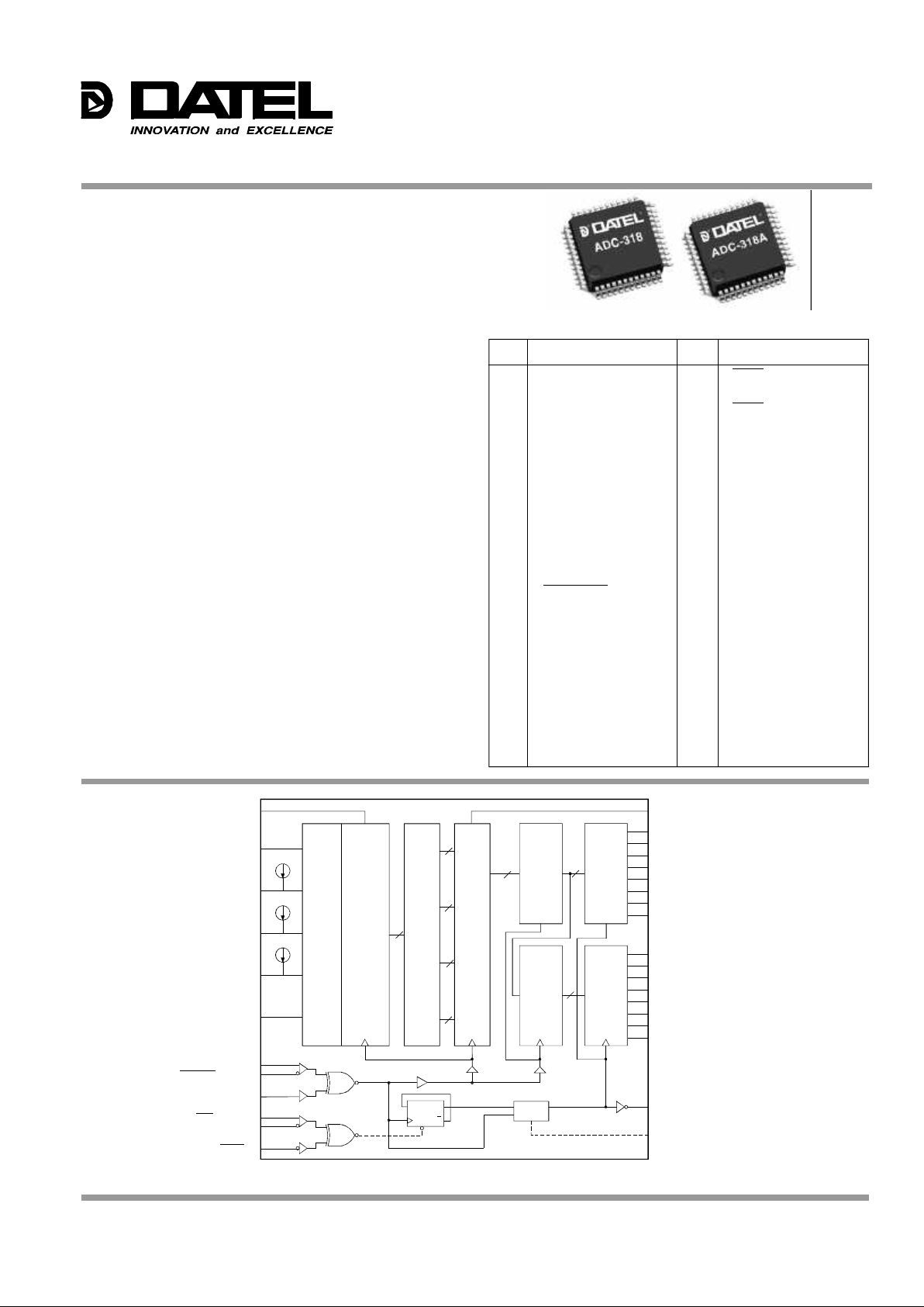
Figure 1. ADC-318/318A Functional Block Diagram
1 –DVs (Digital) 48 RSET ECL/PECL
2 REF. BOTTOM (V
RB) 47 RSET ECL/PECL
3 ANALOG GROUND 46 RSET TTL
4 REF. MID POINT (V
RM1) 45 SELECT
5 +AV
S (Analog) 44 INV
6 ANALOG IN (V
IN) 43 TTL CLOCK OUT
7 REF. MID POINT (V
RM2) 42 +DVS2 (Digital)
8 +AV
S (Analog) 41 DIGITAL GROUND 2
9 REF. MID POINT (V
RM3) 40 A BIT 1 (MSB)
10 ANALOG GROUND 39 A BIT 2
11 REF. TOP (V
RT) 38 A BIT 3
12 DIGITAL GROUND 3 37 A BIT 4
13 A/D CLOCK ECL/PECL 36 A BIT 5
14 A/D CLOCK ECL/PECL 35 A BIT 6
15 A/D CLOCK TTL 34 A BIT 7
16 NO CONNECTION 33 A BIT 8 (LSB)
17 NO CONNECTION 32 DIGITAL GROUND 2
18 NO CONNECTION 31 +DV
S2 (Digital)
19 +DV
S2 (Digital) 30 +DVS1 (Digital)
20 DIGITAL GROUND 2 29 DIGITAL GROUND 1
21 B BIT 8 (LSB) 28 B BIT 1 (MSB)
22 B BIT 7 27 B BIT 2
23 B BIT 6 26 B BIT 3
24 B BIT 5 25 B BIT 4
INPUT/OUTPUT CONNECTIONS
PIN FUNCTION PIN FUNCTION
256
ENCODER
COMPARATOR
SELECT
6
11
9
7
4
2
13
14
15
48
47
46
V
IN
V
RT
V
RM3
VRM2
VRM1
V
RB
A/D CLOCK ECL/PECL
A/D CLOCK TTL
RSET ECL/PECL
RSET TTL
RESISTOR
MATRIX
6-BIT LATCH
AND ENCODER
6
6
6
6
DELAY
D Q
Q
8 8
6
A
LATCH
B
LATCH
A
TTL
OUTPUT
B
TTL
OUTPUT
TTL
44 INV
33 BIT 8 (LSB)
34 BIT 7
35 BIT 6
36 BIT 5 A OUTPUT
37 BIT 4
38 BIT 3
39 BIT 2
40 BIT 1 (MSB)
21 BIT 8 (LSB)
22 BIT 7
23 BIT 6
24 BIT 5 B OUTPUT
25 BIT 4
26 BIT 3
27 BIT 2
28 BIT 1 (MSB)
43 CLOCK OUT
45 SELECT
A/D CLOCK ECL/PECL
RSET ECL/PECL
GENERAL DESCRIPTION
The ADC-318 and ADC-318A are 8 bit monolithic bipolar,
full flash A/D converters. Though they have high, 120MHz
(ADC-318) and 140MHz (ADC-318A), sampling rates, their
input logic level, including the start convert pulse, is TTL,
ECL and PECL compatible. Digital outputs are also TTL
compatible and allow a straight output or a programmable
1:2 de-multiplexed output.
The ADC-318 and ADC-318A feature ±1/2 LSB max.
integral and differential non-linearity, +5V single or ±5V dual
power supply operation, a low 960mW maximum power
dissipation, 150MHz wide analog input range and excellent
temperature coefficient in a small 48 pin QFP package. The
start convert pulse can have a 50% duty cycle.
The ADC-318 and ADC-318A offer low cost, easy to use
functionality for design engineers.
Page 2
ADC-318, ADC-318A
2
® ®
DIGITAL INPUTS MIN. TYP. MAX. UNITS
A/D Clock Pulse Width (T
PW1)
ADC-318 3.2 — — ns
ADC-318A 3.0 — — ns
A/D Clock Pulse Width (T
PW0)
ADC-318 3.2 — — ns
ADC-318A 3.0 — — ns
RSET Setup Time (T
rs) 3.5 — — ns
RSET Hold Time (T
rh) 0 — — ns
DIGITAL OUTPUTS
Output Voltage "1" (@–2mA) 2.4 — — Volts
Output Voltage "0" (@1mA) — — +0.5 Volts
Output Rise Time (T
r) ➃ — 2 — ns
Output Fall Time (T
f) ➃ — 2 — ns
Output Delay (T
do1) ➄ 1/Fc 1/Fc+1 1/Fc+2 ns
Output Delay (T
do2) ➅ 6.5 8 10 ns
Clockout Output Delay (T
dclk) ➆ 4.5 7 8 ns
PERFORMANCE
Resolution 8 — — Bit
Conversion Rate (f
S)
Straight Mode
ADC-318 100 — — MHz
ADC-318A 100 — — MHz
De-multiplexed Mode
ADC-318 100 — — MHz
ADC-318A 100 — — MHz
Sampling Delay (T
dS) 3 4.5 6 ns
Aperture Jitter (Taj) — 10 — ps
Integral Linearity Error — — ±0.5 LSB
Diff. Linearity Error — — ±0.5 LSB
S/N Ratio ➇
ADC-318
(@f
IN = 1kHz) — 46 — dB
(@f
IN = 29.999MHz) — 40 — dB
ADC-318A
(@f
IN = 1kHz) — 46 — dB
(@f
IN = 34.999MHz) — 40 — dB
Error Rate
ADC-318
(@f
IN = 1kHz) ➈ — — 10
-12
TPS
(@f
IN = 29.999MHz) — — 10
-9
TPS
(@fIN = 24.999MHz)➉ — — 10
-9
TPS
ADC-318A
(@f
IN = 1kHz) ➈ — — 10
-12
TPS
(@f
IN = 34.999MHz) — — 10
-9
TPS
(@fIN = 24.999MHz)➉ — — 10
-9
TPS
POWER REQUIREMENTS
Supply Voltage
One Power Supply
(+AV
S, +DVS 1,2) +4.75 +5.0 +5.25 Volts
One Power Supply (DGND3) +4.75 +5.0 +5.25 Volts
One Power Supply (–DV
S) –0.05 0 +0.05 Volts
Two Power Supply
(+AV
S, +DVS 1,2) +4.75 +5.0 +5.25 Volts
Two Power Supply (DGND3) –0.05 0 +0.05 Volts
Two Power Supply (–DV
S) –5.5 –5.0 –4.75 Volts
ADC-318
Supply Current (+I
S) 125 145 185 mA
Supply Current (–I
S) 0.4 0.6 0.8 mA
ADC-318A
Supply Current (+z
S) 110 150 185 mA
Supply Current (–z
S) 0.4 0.6 0.8 mA
ANALOG INPUTS MIN. TYP. MAX. UNITS
Input Voltage — +2 to +4 — Volts
Input Resistance 4 — 50 kΩ
Input Current 0 — 500 µA
Input Capacitance ➀ — 21 — pF
Input Bandwidth
V
IN = 2Vp-p, –3dB 150 — — MHz
REFERENCE INPUTS
Reference Voltage
VRT +2.9 — +4.1 Volts
VRB +1.4 — +2.6 Volts
VRT–VRB 1.5 — 2.1 Volts
Reference Resistance 75 115 155 Ω
Reference Current 9.7 17.4 28 mA
V
RT Offset Voltage 2 — 15 mV
V
RB Offset Voltage 2 — 10 mV
DIGITAL INPUTS
ECL, PECL
Input Voltage "1"
DGND3–1.05 — DGND3–0.5 Volts
Input Voltage "0"
DGND3–3.2 — DGND3–1.4 Volts
Threshold Voltage —
DGND3–1.2 — Volts
Input Current "1" ➁ –50 — +50 µA
Input Current "0" ➁ –75 — 0 µA
Voltage Difference 0.4 0.8 — Volts
TTL
Input Voltage "1" +2.0 — — Volts
Input Voltage "0" — — +0.8 Volts
Threshold Voltage — +1.5 — Volts
Input Current "1" ➂ –50 — 0 µA
Input Current "0" ➂ –500 — 0 µA
Select
Input Voltage "1" — +DVS1 —
Output Voltage "0" — +DGND1 —
Input Capacitance — — 5 pF
PARAMETERS LIMITS UNITS
Supply Voltage (+AVS, +DVS, 1,2) –0.5 to +7.0 Volts
Supply Voltage (AGND, DGND 1, 2) –0.5 to +7.0 Volts
Supply Voltage (DGND 3) –0.5 to +7.0 Volts
Supply Voltage (–DVS) ➀ –0.5 to +7.0 Volts
Supply Voltage (–DVS) ➁ –7.0 to +0.5 Volts
Reference Voltage (VRT) +2.7 to +AVS Volts
Reference Voltage (VRB) VIN –2.7 to +AVS
Reference Voltage (VRT–VRB1) 2.5 Volts
Input Voltage, analog (VIN) VRT –2.7 to +AVS Volts
Input Voltage, digital
ECL –DVS to +0.5 Volts
PECL –0.5 to DGND3 Volts
TTL –0.5 to +DVS1 Volts
Diff. Voltage between Pin ➂ 2.7 Volts
Power Dissipation, max. ➃ 2 W
ABSOLUTE MAXIMUM RATINGS
Footnote:
➀ Single Supply
➁ Dual Supply
➂ A/D Clock–A/D Clock and RESET–RESET of ECL/PECL logic inputs.
➃ With ADC-318 mounted on a 50x50mm glass fiber base
epoxy board, 1.6mm thick.
FUNCTIONAL SPECIFICATIONS
(Typical at TA = 25°C, VRT = +4V, VRB = +2V, DGND3 = +DVS1= +DVS2 = +AVS =
+5V, –DVS = 0V, PECL Logic, unless otherwise specified.)
13
13
13
11
11
11
11
11
11
Page 3
ADC-318, ADC-318A
3
® ®
318A requires that the characteristic impedance of all input/
output logic and analog input lines be properly matched.
2. Power supply lines and grounding may effect the performance of the ADC-318 and ADC-318A. Separate and
substantial AGND and DGND ground planes are required.
These grounds have to be connected to one earth point
underneath the device. There are three digital grounds,
DGND1 (pin 29), DGND2 (pins 20, 32, 41) and DGND3 (pin
12). These DGND 's are separated internally. DGND1 and
DGND2 are always connected externally but DGND3 shall
be connected differently depending on whether the single or
dual power supply mode is used, as explained later.
The ADC-318 and ADC-318A have separate +AVs and
+DVs pins. It is recommended that both +AVs and +DVs be
powered from a single source. Other external digital circuits
must be powered with a separate +DVs. Layouts of +AVs
and +DVs lines must be separated like the GND lines to
avoid mutual interference and are connected to a point
through an LC filter. There are two digital supplies +DVs1
(pin 30) and +DVs2 (pins 19, 31, 42). These are also
separated internally. These must be tied together outside
while in use. Bypassing all power lines with a 0.1uF ceramic
chip capacitor and the use of multilayered PC boards is
recommended.
3. The analog input terminal (pin 6) has 21pF of input capacitance. The input signal has to be given via a buffer amplifier
which has enough driving power. Make lead wires as short
as possible and use chip resistors and capacitors to avoid
parasitic capacitance and inductance.
4. The use of a buffer amplifier and bypass capacitors is also
recommended on the reference input terminals VRT (pin 11)
and VRB (pin 2). The analog input range is determined by
POWER REQUIREMENTS (cont.)
Power Dissipation
ADC-318 680 780 980 mW
ADC-318A 570 790 960 mW
PARAMETERS
Operating Temp. Range, Case
ADC-318, 318A –20 — +75 °C
Thermal Impedance
θja — 62.5 — °C/Watt
Storage Temperature Range –65 — +150 °C
Package Type 48-pin, plastic QFP
Weight 0.25 ounces (0.7 grams)
Footnotes:
➀ VIN = +3V +0.07Vrms
➁ VIH = DGND3–0.8V
VIL = DGND3–1.6V
➂ VIH = 3.5V
VIL = 0.2V
➃ TTL, 0.8 to 2.0V, CL = 5pF
➄ DMUX Mode, CL = 5pF; FC = Clock
frequency
➅ Straight Mode, CL = 5pF
➆ CL = 5pF
➇ VIN = FS, DMUX mode
➈ VIN = FS, DMUX mode, Error >16LSB
➉ VIN = FS, Straight mode, Error >16LSB
"Times Per Sample"
Mounted on 50x50mm, 1.6mm thick
glass fiber base epoxy board
TECHNICAL NOTES
1. The ADC-318 and ADC-318A are ultra high speed full flash
A/D converters that have 120MHz and 140MHz sampling
rates respectively. The ADC-318 and ADC-318A are fully
interchangeable products with the exception of their
sampling rates. Their inputs are TTL, ECL and PECL
compatible and their outputs are TTL compatible. Obtaining
fully specified performance from the ADC-318 and ADC-
12
11
12
Figure 2-1: One Power Supply Operation (TTL, PECL)
Figure 2-2: Two Power Supply Operation (ECL)
Note: All capacitors not otherwise designated are 0.1µF
+ +
+
+
5V(A)
10µF
10µH 5V(D)
10µF
85 19 30 31 42
10µF
2
V
RB
+2V
ANALOG IN
+2V to +4V
4
6
7
9
11
VRT
+4V
10µF
A/D CLOCK
15
13
14
48
47
46
3 10
20 29 32
41
45
44
43
TTL
CLOCK OUT
5V(D)
28 B BIT 1
27 B BIT 2
26 B BIT 3
25 B BIT 4
24 B BIT 5
23 B BIT 6
22 B BIT 7
21 B BIT 8
LSB
MSB
40 A BIT 1
39 A BIT 2
38 A BIT 3
37 A BIT 4
36 A BIT 5
35 A BIT 6
34 A BIT 7
33 A BIT 8
LSB
MSB
ADC-318
12
1
TTL
PECL
ADC-318A
5V(D)
+ +
+
+
+
5V(A)
10µF
10µH 5V(D)
10µF
85 19 30 31 42
10µF
2
V
RB
+2V
ANALOG IN
+2V to +4V 4
6
7
9
11
VRT
+4V
10µF
ECL
A/D CLOCK
A/D CLOCK
15
13
14
48
47
46
3 10
1 12
20 29 32
41
10µF
5V(D)
45
44
43
TTL
CLOCK OUT
28 B BIT 1
27 B BIT 2
26 B BIT 3
25 B BIT 4
24 B BIT 5
23 B BIT 6
22 B BIT 7
21 B BIT 8
LSB
MSB
40 A BIT 1
39 A BIT 2
38 A BIT 3
37 A BIT 4
36 A BIT 5
35 A BIT 6
34 A BIT 7
33 A BIT 8
LSB
MSB
ADC-318
ADC-318A
5V(D)
5V(D)
Page 4

ADC-318, ADC-318A
4
® ®
Figure 2-3: A/D Clock Input Connection Figure 2-4: Digital Input/Output Connections
SIGNAL DIGITAL OUTPUT CODE (A,B OUTPUT)
INPUT INV=1 INV=0
VOLTAGE LSB MSB LSB MSB
VRT 11111111 00000000
VRM2 10000000 01111111
01111111 10000000
VRB 00000000 11111111
Table 4: Digital Output Coding
DIGITAL INPUT SUPPLY
LEVEL –DVS DGND3 VOLTAGES
TTL 0V +5V +5V
PECL 0V +5V +5V
ECL –5V 0V ±5V
Table 3: Logic Input Level vs. Power Supply Settings
11
12
13 14 15 16 17 18
TTL LEVEL CLOCK INPUT
A/D CLOCK
A/D CLOCK
A/D CLOCK
ECL, PECL LEVEL CLOCK INPUTS
ADC-318
ADC-318A
TTL LEVEL RESET INPUT
RSET
RSET
RSET
ECL, PECL LEVEL
RESET INPUTS
2
1
48 47 46 45 44 43 42
TTL CLOCK OUT
COMPLEMENTARY BINARY
STRAIGHT BINARY
OUTPUT CODING
STRAIGHT DATA OUT
DEMULTIPLEXED DATA OUT
A/D CONVERSION MODE
5V(D)
5V(D)
ADC-318
ADC-318A
the reference input voltages given to VRT and VRB. Keep
the ranges of V within values shown in this data sheet.
Standard settings are VRT = +4.0V, V input range from
+2 to +4V. This setting can be varied to VRT = +3.5V,
VRB = +2V and 1.5V p-p analog input range, depending
on your selection of amplifiers which may provide less
than +4V output.
5. The ADC-318 and ADC-318A have resistor matrix taps at
VRM1 (pin 4), VRM2 (pin 7) and VRM3 (pin 9). These pins
provide ¼, ½ and ¾ full scale of VRT-VRB voltage respectively. These outputs may be used to adjust the integral
non-linearity. Bypass these pins to GND with 0.1uF ceramic
chip capacitors.
6. A/D CLK input and RSET/RSET inputs are TTL or ECL,
PECL (Positive ECL) compatible. Pins are provided
individually. TTL or PECL is available with +5V single power
applied. ECL is available with ±5V dual power applied. The
connections of –DVs (pin 1) and DGND3 (pin12) are
different depending on the power supply mode used. Refer
to Figures 2-1 and 2-2.
a. For +5V single power (TTL or PECL) –DVs (pin 1) is
connected to DGND. DGND3 (pin 12) is connected
to +5V power.
b. For ±5V dual power (ECL) –DVs (pin 1) is connected
to –5V power. DGND3 (pin 12) is connected to DGND.
7. When the A/D CLK is driven with ECL or PECL, A/D CLK
(pin 13) and A/D CLK (pin 14) are to be driven by differential logic inputs to avoid unstable performance at critically
high speeds. If a risk of unstable performance is acceptable, single logic input can be used opening A/D CLK (pin
14). The A/D CLK pin should be bypassed to DGND with a
0.1uF ceramic capacitor. When connected this way there
will be a voltage of DGND –1.2V on the A/D CLK pin. This
voltage can not be used as a threshold voltage for ECL or
PECL. Input the A/D CLK pulse to pin 15 when TTL is
selected.
8. The ADC-318 and ADC-318A have RSET/RSET input pins.
An internal frequency half divider can be initialized with
inputs to these pins. With ECL or PECL, differential inputs
are given to RSET (pin 48) and RSET (pin 47). This
function can be achieved with a single input, leaving pin 47
open and bypassing to DGND with a 0.1uF ceramic chip
capacitor. The voltage level of pin 47 is the threshold
voltage of ECL or PECL. Use RSET (pin 46) for TTL.
9. SELECT (pin 45) is used to set output mode. Connection of
this pin to DGND selects the straight output mode and
connection to +DVs selects the 1:2 de-multiplexed output
mode. The maximum sampling rates are 100MHz for straight
mode (For both models, ADC-318 and ADC-318A) and
120MHz (ADC-318) and 140MHz (ADC-318A) for demultiplexed mode. Refer to figure 2-4. There is an application where a multiple number of ADC-318/318A's are used
with a common A/D CLK and outputs are in de-multiplexed
mode. In this case, the initial conditions of the frequency half
divider of each A/D Converter are not synchronized and it is
possible that each converter may have one clock maximum
of timing lag. This lag can be avoided by giving a common
RSET pulse to all converters at power ON. (See Figure 3-3
and 3-4, timing diagrams.)
10.The ADC-318 and ADC-318A have a TTL compatible CLK
OUT (pin 43). Since the rising edge of this pulse can provide
Setup and Hold time of output data, regardless of the output
mode, this signal can be used as synchronization pulse for
external circuits. Data output timing is different for the
straight mode and the de-multiplexed mode. See the timing
chart Figure 3.
11. INV (pin 44) is used to invert polarity of the TTL compatible
output data from both A and B ports. Leaving this pin open
or connected to +DVs makes the output positive true and
connection to DGND makes it negative true logic. See
input/output code table, Table 4.
Page 5

ADC-318, ADC-318A
5
® ®
Figure 3-1: Demultiplexed Data Output (Select-Pin: +DVS or left open, 120MHz max. Clock Frequency)
Figure 3-2: Straight Data Output (Select-Pin: DGND, 100MHz max. Clock Frequency)
Figure 3-3: Parallel Operation without RSET Pulse Figure 3-4: Parallel Operation using RSET Synchronization
A/D CLOCK
CLOCK OUT 1
DATA OUT 2
(A,B)
CLOCK OUT 2
DATA OUT 1
(A,B)
A/D CLOCK
A/D CLOCK
ADC-318/318A
RSET
A/D CLOCK
CLOCK OUT 1
DATA 1 (A, B)
DATA 2 (A, B)
CLOCK OUT 2
A/D CLOCK
ADC-318/318A
RSET
(2)
(1)
8
8
8
8
A/D CLOCK
CLOCK OUT 1
DATA OUT 2
(A,B)
CLOCK OUT 2
DATA OUT 1
(A,B)
RSET
A/D CLOCK
A/D CLOCK
ADC-318/318A
RSET
A/D CLOCK
A/D CLOCK
ADC-318/318A
RSET
RSET
8
8
8
8
(2)
(1)
CLOCK OUT 1
DATA 1 (A, B)
DATA 2 (A, B)
CLOCK OUT 2
T
ds
N-1
N
N+1
N+2
N+3
N+4
N+5
ANALOG SIGNAL A
IN
T
PW1
T
PW0
A DATA OUTPUT
B DATA OUTPUT
3.5ns min.
CLOCK OUT
RSET
A/D CLOCK
3ns min. 6ns max
T
N+6
N+7
2.0V
0.8V
2.0V
0.8V
RESET PERIOD
Td clock
4.5ns min. 8ns max.
2.0V
0.8V
Tdo1
T T
0ns min.
Trh Trs Trh Trs
Tdo2
N+3
N
N+2
2.0V
0.8V
T+2ns max.
~~
N+1
6.5ns min. 10ns max.
TPW1, min
TPW0, min 3.2ns 3.0ns
3.2ns 3.0ns
318 318A
T
ds
N-1
N
N+2
N+3
ANALOG SIGNAL A
IN
TPW1 TPW0
A DATA OUTPUT
CLOCK OUT
(inverted A/D CLOCK OUT)
RSET
A/D CLOCK
N+1
N-3N-4 N-2
N-4 N-3
N-1
N-2
N
N-1
T
d clock
6.5ns min. 10ns max.
B DATA OUTPUT
T
2.0V
0.8V
N-5
2.0V
0.8V
Tdo2
2.0V
0.8V
4.5ns min. 8ns max.
3ns min. 6ns max.
TPW1, min
TPW0, min 3.2ns 3.0ns
3.2ns 3.0ns
318 318A
Page 6

ADC-318, ADC-318A
6
® ®
APPLICATION
This device can be used in applications where 3 parallel
channels are synchronized. Conversion speed is the highest
in the de-multiplexed mode. It is difficult to control timing of
three channels at such a high speed. Two practical ways to
maintain timing for reading data into the system are given.
1. Clock output of one A/D is used in reading data of
other channels
Time delay of Clock Output and Output Data are
specified as:
Td clk (CLK OUT Delay) ; 4.5nSec min., 8.0nsec max.
Tdo2 (Output Data Delay); 6.5nSec min., 10nsec max.
These values apply over the operating temperature and
supply voltage ranges. Timing control of Tset (Setup Time)
seems to be very critical. It tends to lead by 0.5nsec as
temperature and supply voltages go lower. When A/D
converters for 3 channels are used on the same board,
temperature and supply voltages tend to change in the
same direction and effects caused by these changes
are negligible.
A/D CLCK
RSET
CLK OUT
OUTPUT
DATA (A, B)
Td clck min.
5.0nS
(4.5nS)
7.5nS
(8.0nS)
7.0nS
(6.5nS)
9.5nS
(10nS)
Th reset
14nS
Tset min. 2.5nS
Thold min. 6.5ns
Td clck max.
Tdo2 min.
Tdo2 max.
Tdclk and Tdo2 at Ta=25°C , +Vs=+5.0V are;
Td clk: 5.0nsec min., 7.5nsec max.
Tdo2: 7.0nsec min., 9.5nsec max.
So long as devices are located on the same board and take
power from the same source, 2.5nsec min. of setup time for
data reading can be secured even though temperature and
power supply voltages vary. A timing diagram at 140MHz
sampling rate is shown in Figure 4a.
2. To read output data of 3 channels into a gate array
Both output data lines and each clock output are read into a
gate array if the digital circuits after the A/D conversion
consist of one high speed gate array. An AND gate is
prepared to take the AND of each output signal which is
used for reading output data. The slowest rise time clock
determines the system clock. Thus adequate setup time is
secured. This method can be employed only when a high
speed gate array is used. The setup time is delayed by the
delay time of the AND gate. The use of a discrete IC gate is
not recommended because of its time delay characteristics.
See Figure 4b
Figure 4a: Timing diagram 1
Figure 4b: Timing diagram 2
*Values in parenthesis are for
the entire operating temperature
and operating power supply ranges
*Values in parenthesis are for
the entire operating temperature
and operating power supply ranges
A/D CLCK
RSET
CLK OUT
OUTPUT
DATA (A, B)
Td clck min.
5.0nS
(4.5nS)
7.5nS
(8.0nS)
7.0nS
(6.5nS)
9.5nS
(10nS)
Th reset
14nS
Td clck max.
Tdo2 min.
Tdo2 max.
Tset min.
5.0nS+XnS
Thold min.
6.5nS–XnS
GATE ARRAY CLK
(CLK OUT 1, CLK OUT 2, CLK OUT 3)
Page 7
ADC-318, ADC-318A
7
® ®
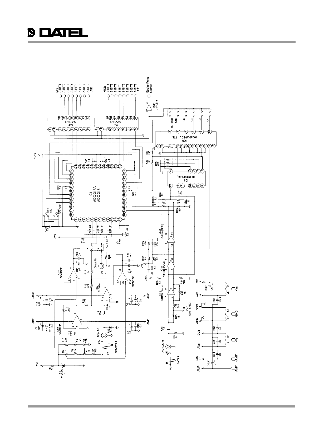
1. The evaluation circuit shown employs PECL logic. Because of this, a 1Vp- p, 0V center, sine wave must be used as
the clock input (A/ D CLK) at CN3.
2. When analog signals are taken from the CN1 amplifier input “A” must be left open while “B” is short circuited. The
analog input signals at CN1 must be less than 800mVp- p, 0V and zero centered. The +AMP and –AMP supply pins
on the input amplifier are normally connected to +/- 5V which, along with the gain of -2 used with the CLC- 404 in this
circuit, will limit the amplifiers output dynamic range. To increase the amplifiers output dynamic range the +AMP pin
can be connected to +7V and the –AMP connected to -3V. V RT and V RB may require adjustment in this case.
3. When analog signals are input from CN2, the direct input, AC coupling can be achieved by inserting a 0.1µF
capacitor at” A” and a 10kOhm resistor at “B”. It is not necessary to be concerned about the output voltage of the
input amplifier. V RT may be limited in this case by NJM3403. The input voltage to the NJM3403 amplifier can be
adjusted to correct. Both V RT and V RB can be trimmed.
Figure 5: Evaluation Circuit Diagram
Page 8

DATEL, Inc. 11 Cabot Boulevard, Mansfield, MA 02048-1151
Tel: (508) 339-3000 (800) 233-2765 Fax: (508) 339-6356
Internet: www.datel.com Email: sales@datel.com
Data sheet fax back: (508) 261-2857
DATEL makes no representation that the use of its products in the circuits described herein, or the use of other technical information contained herein, will not infringe upon existing or future patent rights. The descriptions contained herein
do not imply the granting of licenses to make, use, or sell equipment constructed in accordance therewith. Specifications are subject to change without notice. The DATEL logo is a registered DATEL, Inc. trademark.
DATEL (UK) LTD. Tadley, England Tel: (01256)-880444
DATEL S.A.R.L. Montigny Le Bretonneux, France Tel: 01-34-60-01-01
DATEL GmbH Munchen, Germany Tel: 89-544334-0
DATEL KK Tokyo, Japan Tel: 3-3779-1031, Osaka Tel: 6-354-2025
DS-0358 5/98
ADC-318, ADC-318A
® ®
ISO 9001
ISO 9001
REGISTERED
.602
±.016
(15.3)
+.016
–.004
.472
0.031
(0.8)
0.012
+.006
–.004
48
37
36 25
24
13
121
0.004
+.008
–.004
.531
(13.5)
0.006
+.004
–.002
0.035 ±.008
0.087
+.014
–.006
(12.0)
(0.3)
(2.2)
(0.9)
(0.1)
(0.15)
ORDERING INFORMATION
ADC-318 8-bit, 120MHz Flash A/D
ADC-318A 8-bit, 140MHz Flash A/D
Figure 6: Typical Performance Curve
MECHANICAL DIMENSIONS INCES (MM)
170
160
150
140
130
–25 25
75
TA –Ambient Temperature (°C)
170
160
150
140
130
0 50 140
Conversion Rate (MHz)
100
20
15
10
–25 25
75
10-
6
10-
7
10-
8
10-9
10-10
140 180160
40
30
20
3 10
50
Input Frequency (MHz)
50
1 5 30
Fig. 4-1:
Supply Current vs. Temperature
Supply Current (mA)
Fig. 4-2:
Supply Current vs. Conversion Rate
Supply Current (mA)
Reference Current (mA)
Fig. 4-3:
Reference Current vs.Temperature
Fig. 4-4:
Error Rate vs. Conversion Rate
Fig. 4-5:
SNR+THD vs. Input Signal Frequency
SNR+THD (dB)
TA –Ambient Temperature (°C) Conversion Rate (MHz)
Error Rate (TPS)
Sine Wave Curvefit Test
1.0000
(256)
0.0000
(128)
0.5000
(192)
–0.500
(64)
VOLT/ (CODE)
8
7
6
5
4
3
2
1
0
–1
–2
–3
–4
–5
–6
–7
–8
DEVIATION (LSB)
S/N Ratio 48.7dB
7.8 Effective Bits
Conditions
Sampling Frequency 120MHz
Signal Frequency 996kHz
4096 Points
ADC-318A
ADC-318
ADC-318 ADC-318A
fin = Fc/4–1KHz
Error> 16LSB
170
160
150
140
130
–25 25 75
TA –Ambient Temperature (°C)
Fig. 4-8:
Maximum Conversion Rate vs.Temperature
Conversion Rate (MHz)
ADC-318
ADC-318A
ADC-318: FC=120MHz
ADC-318A: FC=140MHz
90
80
70
2
°C
0
SNR+THD (dB)
Fig. 4-6:
Allowable Ambient Temperature vs. Air Flow
1 3 m/s
60
Four-layer board
Double-layer board
Single-layer board
ADC-318A
ADC-318
200
100
0
2 3
4
VIN Pin Voltage (V)
Fig. 4-7:
Analog Input Current vs.Voltage Inputs
Analog Input Current (µA)
VRT = +4V
VRB = +2V
Fig. 4-9: Sine Wave Curvefit Test
 Loading...