

Page 1
INPUT/OUTPUT CONNECTIONS
PLASTIC DIP PACKAGE
PIN FUNCTION PIN FUNCTION
1 BIT 1 (MSB) 28 MINV
2 BIT 2 27 V
M
3 BIT 3 26 V
B
4 BIT 4 25 ANALOG GND
5 DIGITAL GND 24 NO CONNECT
6 +5V POWER 23 ANALOG INPUT
7 –5.2V POWER 22 NO CONNECT
8 –5.2V POWER 21 ANALOG INPUT
9 –5.2V POWER 20 NO CONNECT
10 +5V POWER 19 ANALOG GND
11 DIGITAL GND 18 V
T
12 LINV 17 CLOCK INPUT
13 BIT 5 16 BIT 8 (LSB)
14 BIT 6 15 BIT 7
FEATURES
• 8-bit resolution
• 20MHz conversion rate
• ±1/2LSB maximum nonlinearity
• 8MHz input bandwidth
• Low power consumption, 375mW
• TTL compatible
• Single or dual supply operation
GENERAL DESCRIPTION
Datel’s ADC-304 is an 8-bit, 20MHz analog-to-digital flash
converter. The ADC-304 offers many performance features not
obtainable from other flash A/D’s.
Key reatures include a low power dissipation of 375mW and
TTL-compatible outputs. A wide analog input bandwidth of
8MHz (–3dB) allows operation without the need of a samplehold. Also, single +5V supply operation is obtainable with an
input range of +3 to +5V, eliminating the need for an additional
power supply. A 0 to –2V input range is available with ±5V
supply operation.
Another novel feature of the ADC-304 is its user-selectable
output coding. The MINV and LINV pins allow selection of
binary, complementary binary, and if external offset circuitry is
used for bipolar inputs, offset binary, two’s complement and
complementary two’s complement coding.
The ADC-304 is supplied in a 28-pin plastic DIP or a 28-pin
plastic SOP package. Operating temperature range is –20 to
+75°C. Storage temperature range is –55 to +150°C.
INPUT/OUTPUT CONNECTIONS
PLASTIC SOP PACKAGE
PIN FUNCTION PIN FUNCTION
1 ANALOG INPUT 28 ANALOG INPUT
2 V
B
SENSE 27 VT SENSE
3 ANALOG GND 26 ANALOG GND
4 V
B
25 V
T
5 V
M
24 CLOCK INPUT
6 NO CONNECT 23 BIT 8 (LSB)
7 MINV 22 BIT 7
8 BIT 1 (MSB) 21 BIT 6
9 BIT 2 20 BIT 5
10 BIT 3 19 LINV
11 BIT 4 18 DIGITAL GND
12 DIGITAL GND 17 +5V POWER
13 +5V POWER 16 OVERRANGE
14 –5.2V POWER 15 –5.2V POWER
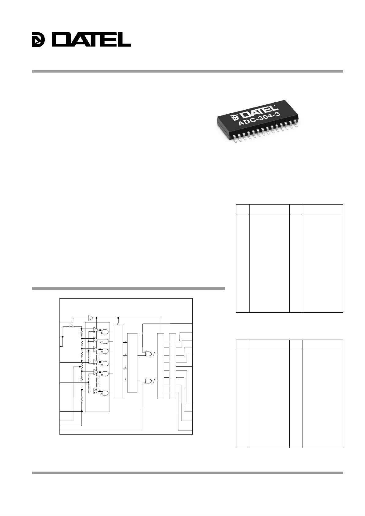
Figure 1. ADC-304 Functional Block Diagram
INNOVATION and EX C ELL E N C E
® ®
BIT 1 (MSB)
BIT 2
BIT 3
BIT 4
OVERRANGE ➀
CLOCK
INPUT
BIT 8 (LSB)
LINV
BIT 7
BIT 6
BIT 5
ANALOG
INPUT
VB
VB SENSE ➀
R/2
R/2
R/2
R
R
R
R
7
6
6
6
2
5
6
-
T
O
-
2
4
B
I
T
E
N
C
O
D
E
R
2
4
-
T
O
-
8
B
I
T
E
N
C
O
D
E
R
L
A
T
C
H
O
U
T
P
U
T
B
U
F
F
E
R
6
COMPARATOR
LATCH
1
256
129
128
3
2
1
VM
VT SENSE ➀
MINV
➀
THESE PINS ARE AVAILABLE ON SOP PACKAGE ONLY
V
T
ANALOG
INPUT
ADC-304
8-Bit, 20MHz, Low-Power
Flash A/D Converters
DATEL, Inc., 11 Cabot Boulevard, Mansfield, MA 02048-1151 (U.S.A.) • Tel: (508) 339-3000 Fax: (508) 339-6356 • For immediate assistance (800) 233-2765
Page 2
® ®
ADC-304
FUNCTIONAL SPECIFICATIONS
Unless otherwise noted, the following specifications apply to the ADC-304 when used
either with a single or dual power source. The test conditions are:
For single power supply operation: For dual power supply operation:
+V
S
= +5V, DIG GND = 0V +VS = +5V, DIG GND = 0V
–V
S
= 0V, VT = +5V –VS = –5.2V, VT = 0V,
V
B
= +3V, TA = +25°C VB = –2V, TA = +25°C
ANA GND = +5V, f
s = 20MHz ANA GND = 0V, fs = 20MHz
ANALOG INPUTS MIN. TYP. MAX. UNITS
Input Range V
B
V
T
Volts
Input Capacitance — 30 35 pF
Input Bias Current 15 50 100 µA
Offset Voltage
V
T
–8 –13 –19 mV
V
B
0 +5 +11 mV
DIGITAL INPUTS
Logic Levels
Logic “1” +2.0 — — Volts
Logic “0” — — +0.8 Volts
Logic Input Currents
Logic “1” — –100 –150 µA
Logic “0” –0.1 –0.32 –0.5 mA
PERFORMANCE
Conversion Rate ➀ 20 — — MHz
Integral Nonlinearity — — ±1/2 LSB
Differential Nonlinearity — — ±1/2 LSB
Differential Gain Error ➁ — — 1.5 %
Differential Phase Error ➁ — — 0.5 degrees
Aperture Delay Ta 5 7 9 ns
Aperture Uncertainty — 30 — ps
Signal-to-Noise and Distortion
(V
in = full scale, fs = 20MHz)
f
in = 1MHz 47 dB
f
in = 5MHz 43 dB
f
in = 10MHz 35 dB
Clock Pulse Width
Tpw1 35 — — ns
Tpw0 10 — — ns
Reference Pin Current 11 15 18 mA
Reference Resistance (V
T
to VB) — 130 — Ohms
Reference Input (dual supply)
V
T
–0.1 0 +0.1 Volts
V
B
–1.8 –2.0 –2.2 Volts
Footnotes:
➀ f
in = 1kHz, ramp
➁ NTSC 40 IRE-modulated ramp, f
s = 14.3MHz
ABSOLUTE MAXIMUM RATINGS
PARAMETERS LIMITS UNITS
Supply Voltages +V
S
to GND 0 to +6 Volts
–V
S
to GND 0 to –6 Volts
Input Voltage (Analog) Vin –V
S
to (ANA GND + 0.3) Volts
(dual power supply)
Input Voltage (Reference) V
T
, VB, V
M
–VS to (ANA GND + 0.3) Volts
(dual power supply)
❘ V
T
– VB ❘ 2.5 Volts
Input Current I
M
–3.0 to +3.0 mA
Input Voltage (Digital) Digital Inputs –0.5 to +V
S
Volts
DIGITAL OUTPUTS MIN. TYP. MAX. UNITS
Resolution and Output Coding 8 bits
Straight binary
Complementary binary
Two’s complement
Complementary two’s complement
Logic Levels
Logic “1” +2.7 +3.4 — Volts
Logic “0” — — +0.5 Volts
Logic Loading “1” — –500 — µA
Logic Loading “0” — — +3 mA
Output Data Delay
TDLH 15 20 30 ns
TDHL 22 26 35 ns
POWER REQUIREMENTS
Single Power Supply
Supply Voltage = +V
S
+4.75 +5.0 +5.25 Volts
Supply Voltage = –V
S
— 0 — Volts
Supply Current = +I
S
+56 +71 +91 mA
Power Dissipation 280 355 455 mW
Dual Power Supply
Supply Voltage = +V
S
+4.75 +5.0 +5.25 Volts
Supply Voltage = –V
S
–4.75 –5.2 –5.5 Volts
Supply Current = +I
S
+7 +10 +14 mA
Supply Current = –I
S
–50 –62 –78 mA
Power Dissipation 295 375 476 mW
PHYSICAL/ENVIRONMENTAL
Operating Temperature –20 — +75 °C
Storage Temperature –55 — +150 °C
TECHNICAL NOTES
1. The two DIGITAL GND pins (pins 5 and 11 on the DIP, pins
12 and 18 on the SOP) are not connected to each other
internally and neither are the two +5V POWER pins (6 and
10 on the DIP, 13 and 17 on the SOP). All four pins must be
externally connected to the appropriate pcb patterns. Also,
the DIGITAL GND and ANALOG GND pins are not
connected to each other internally.
2. Layout of the analog and digital sections should be
separated to reduce interference from noise. To further
guard against unwanted noise, it is recommended to
bypass, as close as possible, the voltage supply pins to
their respective ground pins with 1µF tantalum and 0.01µF
ceramic disk capacitors in parallel.
3. The input capacitance of the analog input is much smaller
than that of a typical flash A/D converter. It is necessary to
use an amplifier with sufficient bandwidth and driving power.
The analog input pins are separated internally, so they
should be connected together externally. If the ADC-304 is
driven with a low output impedance amplifier, parasitic
oscillations may occur.
These parasitic oscillations can be prevented by introducing
a small resistance of 2 to 10Ω between the amplifier output
and the ADC-304’s A/D input. This resistance must have a
very low value of series inductance at high frequencies.
Note that each of the analog input pins is divided in this
manner with these resistances. Connect the driving amplifier
as close as possible to the A/D input of the ADC-304.
2
Page 3

ADC-304
® ®
6. The analog input signal is sampled on the positive-going
edge of CLOCK. Corresponding digital data appears at the
output on the negative-going edge of the CLOCK pulse after
a brief delay of 31ns maximum (TDLH, TDHL). Refer to the
Timing Diagram (Figure 3) for more information.
7. Connect all free pins to ANALOG GND to reduce unwanted
noise.
The analog input range is equal to a 2V spread. The
voltage on V
T-VB
will equal 2V. The connection of VT and
ANALOG GND is 2V higher than V
B
. Whether using a
single or dual power supply, the analog input will range from
the value of V
T
to VB. If VT equals +5V, then VB will equal
+3V and the analog input range will be from +3 to +5V.
4. The voltage between V
T
and VB is equivalent to the dynamic
range of the analog input. Bypass V
B
to ANALOG GND
USING a 1µF and a 0.01µF capacitor in parallel. To balance
the characteristics of the ADC-304 at high frequencies,
bypass V
M
with a 0.01µF capacitor to ANALOG GND.
Also, V
M
can be used as a trimming pin for more precise
linearity compensation. A stable voltage source with a
potential equal to V
B
and a 1kΩ potentiometer can be
connected to V
M
as shown in Figure 2 for this purpose.
5. Separate the clock input, CLOCK, from other leads as much
as possible, observing proper EMI and RFI wiring
techniques. This reduces the inductive pick-up of this lead
from interfering with the “clean” operation of the ADC-304.
Figure 3. ADC-304 Timing Diagram
Figure 2.
Improving Linearity Compensation
VM
V
B
0.01µF
+5V
1k
Ω
ANA GND
ANA GND
DUAL SUPPLY OPERATION
ADC-304
ADC-304
0.01µF
VM
V
B
1k
Ω
0.01µF
SINGLE SUPPLY OPERATION
V
B
VB
N DATA VALID
CLOCK
COMPARATOR
OUTPUT
Ta
N(1)
N(2)
N(3)
31ns max.
TDLH
TDHL
N(2) DATA VALID
N(1) DATA VALID
6-BIT LATCH OUTPUT
DATA OUTPUT
BITS 1-8
TPW0
TPW1
ANALOG
INPUT
22ns
max.
31ns max.
TDLH
TDHL
22ns
max.
3
Page 4

MINV
(TTL LEVEL)
ANALOG INPUT
0 to –2V
BIT 8
BIT 7
BIT 6
BIT 5
BIT 4
BIT 3
BIT 2
BIT 1
–2V
CLOCK
LINV
(LSB)
(MSB)
V
IN
+5V
12
15 BIT 6 BIT 7
16(LSB) BIT 8
CLOCK
19
ANA GND
20N.C.
21
ANA IN
22
N.C.
ANA IN
24N.C.
ANA GND
27
VM
MINV
BIT 5
LINV
DIG GND
+5V
–5.2V
–5.2V
–5.2V
+5V
DIG GND
BIT 4
BIT 3
BIT 2
BIT 1(MSB)
4
3
2
1
5
6
7
8
9
11
23
18
13
14
17
28
26
10
25
–5.2V
V
T
VB
MINV
(TTL LEVEL)
ANALOG INPUT
+3 to +5V
BIT 8
BIT 7
BIT 6
BIT 5
BIT 4
BIT 3
BIT 2
BIT 1
+3V
CLOCK
(LSB)
(MSB)
V
IN
+5V
+5V
12
15 BIT 6
BIT 7
16
(LSB) BIT 8
CLOCK
V
T
19
ANA GND
20N.C.
21
ANA IN
22
N.C.
ANA IN
24
N.C.
ANA GND
27
VM
V
B
MINV
BIT 5
LINV
DIG GND
+5V
–5.2V
–5.2V
–5.2V
+5V
DIG GND
BIT 4
BIT 3
BIT 2
BIT 1(MSB)
4
3
2
1
5
6
7
8
9
11
23
18
13
14
17
28
26
10
25
LINV
Figure 4. Connections for +5V Power Supply Operation Figure 5. Connections for ±5V Power Supply Operation
APPLICATION CIRCUITS
Straight Complementary Two’s Complementary
Binary Two’s Complement Complement Binary
Unipolar MINV 0 0 1 1
Scale LINV 0 1 0 1
+FS – 1SLB +4.9922V 11111111 10000000 01111111 00000000
+7/8FS +4.7500V 11011111 10100000 01011111 00100000
+3/4FS +4.5000V 10111111 11000000 00111111 01000000
+1/2FS +4.0000V 01111111 00000000 11111111 10000000
+1/4FS +3.5000V 00111111 01000000 10111111 11000000
+1/8FS +3.2500V 00011111 01100000 10011111 11100000
+1LSB +3.0078V 00000001 01111110 10000001 11111110
Zero +3.0000V 00000000 01111111 10000000 11111111
Table 2. Output Coding for ±5V Power Supply Operation (0 to –2V Signal Input)
Straight Complementary Two’s Complementary
Binary Two’s Complement Complement Binary
Unipolar MINV 0 0 1 1
Scale LINV 0 1 0 1
Zero 0.0000V 11111111 10000000 01111111 00000000
–1LSB –0.0078V 11111110 10000001 01111110 00000001
–1/8FS –0.2500V 11011111 10100000 01011111 00100000
–1/4FS –0.5000V 10111111 11000000 00111111 01000000
–1/2FS –1.0000V 01111111 00000000 11111111 10000000
–3/4FS –1.5000V 00111111 01000000 10111111 11000000
–7/8FS –1.7500V 00011111 01100000 10011111 11100000
–FS + 1SLB –1.9922V 00000000 01111111 10000000 11111111
Table 1. Output Coding for +5V Power Supply Operation (+3 to +5V Signal Input)
NOTE: 28-pin DIP package shown
NOTE: 28-pin DIP package shown
® ®
ADC-304
4
Page 5

ADC-304
® ®
MECHANICAL DIMENSIONS
MODEL PACKAGE
ADC-304 28-pin DIP (plastic)
ADC-304-3 28-pin SOP (plastic)
ADC-304-3
28-Pin SOP (Plastic)
ADC-304
28-Pin DIP (Plastic)
ADC-304
1
15
14
28
1.494 ±0.010
(37.95 ±0.25)
0.022 ±0.004
(0.55 ±0.10)
0.100 TYP.
(2.540)
0.051 ±0.006
(1.30 ±0.15)
0.187 ±0.010
(4.75 ±0.25)
0.118 MIN.
(3.0 MIN.)
0° to 15°
0.011 ±0.003
(0.28 ±0.08)
0.52 ±0.02
(13.2 ±0.3)
0.600
(15.24)
SEATING
PLANE
0.020 MIN.
(0.50 MIN.)
ADC-304
1
15
14
28
0.018 ± 0.004
(0.45 ± 0.1)
0.090 ±0.011
(2.30 ±0.28)
0.30 ±0.01
(7.7 ±0.2)
0.366
(9.3)
0.006 ±0.003
(0.15 ±0.08)
0.050 TYP.
(1.270)
0.41 ±0.02
(10.3 ±0.4)
0.020 ±0.008
(0.5 ±0.2)
0.746 ±0.010
(18.95 ±0.25)
0.007 ±0.005
(0.18 ±0.13)
ORDERING INFORMATION
INNOVATION and EX C ELL E N C E
® ®
DATEL, Inc. 11 Cabot Boulevard, Mansfield, MA 02048-1151
Tel: (508) 339-3000 / Fax: (508) 339-6356
For immediate assistance: (800) 233-2765
DATEL makes no representation that the use of its products in the circuits described herein, or the use of other technical information contained herein, will not infringe upon existing or future patent rights. The descriptions contained herein
do not imply the granting of licenses to make, use, or sell equipment constructed in accordance therewith. Specifications are subject to change without notice. The DATEL logo is a registered DATEL, Inc. trademark.
DS-0075B 10/96
DATEL (UK) LTD. Tadley, England Tel: (01256)-880444
DATEL S.A.R.L. Montigny Le Bretonneux, France Tel: 1-34-60-01-01
DATEL GmbH Munchen, Germany Tel: 89-544334-0
DATEL KK Tokyo, Japan Tel: 3-3779-1031, Osaka Tel: 6-354-2025
ISO 9001
ISO 9001
REGISTERED
 Loading...