Page 1
TL/H/11454
ADC16071/ADC16471 16-Bit Delta-Sigma 192 ks/s Analog-to-Digital Converters
February 1995
ADC16071/ADC16471
16-Bit Delta-Sigma 192 ks/s Analog-to-Digital Converters
General Description
The ADC16071/ADC16471 are 16-bit delta-sigma analogto-digital converters using 64
c
oversampling at
12.288 MHz. A 5th-order comb filter and a 246 tap FIR decimation filter are used to achieve an output data rate of up to
192 kHz. The combination of oversampling and internal digital filtering greatly reduces the external anti-alias filter requirements to a simple RC low pass filter. The FIR filters
offer linear phase response, 0.005 dB passband ripple, and
t
90 dB stopband rejection. The ADC16071/ADC16471’s
analog fourth-order modulator uses switched capacitor
technology. A built-in fully-differential bandgap voltage reference is also included in the ADC16471. The ADC16071
has no internal reference and requires externally applied
reference voltages.
The ADC16071/ADC16471 use an advanced BiCMOS process for a low power consumption of 500 mW (max) while
operating from a single 5V supply. A power-down mode reduces the power supply current from 100 mA (max) in the
active mode to 1.3 mA (max).
The ADC16071/ADC16471 are ideal analog-to-digital front
ends for signal processing applications. They provide a
complete high resolution signal acquisition system that requires a minimal external anti-aliasing filter, reference, or
interface logic.
The ADC16071/ADC16471’s serial interface is compatible
with the DSP56001, TMS320, and ADSP2100 digital signal
processors.
Key Specifications
Y
Resolution 16 bits
Y
Total harmonic distortion
48 kHz output data rate
b
94 dB (typ)
192 kHz output data rate
b
80 dB (typ)
Y
Maximum output data rate 192 kHz (min)
Y
Power dissipation
Ð Active
192 kHz output data rate 500 mW (max)
48 kHz output data rate 275 mW (max)
Ð Power-down 6.5 mW (max)
Key Features
Y
Voltage reference (ADC16471 only)
Y
Fourth-order modulator
Y
64coversampling with a 12.288 MHz sample rate
Y
Adjustable output data rate from 7 kHz to 192 kHz
Y
Linear-phase digital anti-aliasing filter:
Ð 0.005 dB passband ripple
Ð 90 dB stopband rejection
Y
Singlea5V supply
Y
Power-down mode
Y
Serial data interface compatible with popular
DSP devices
Applications
Y
Medical instrumentation
Y
Process control systems
Y
Test equipment
Y
High sample-rate audio
Y
Digital Signal Processing (DSP) analog front-end
Y
Vibration and noise analysis
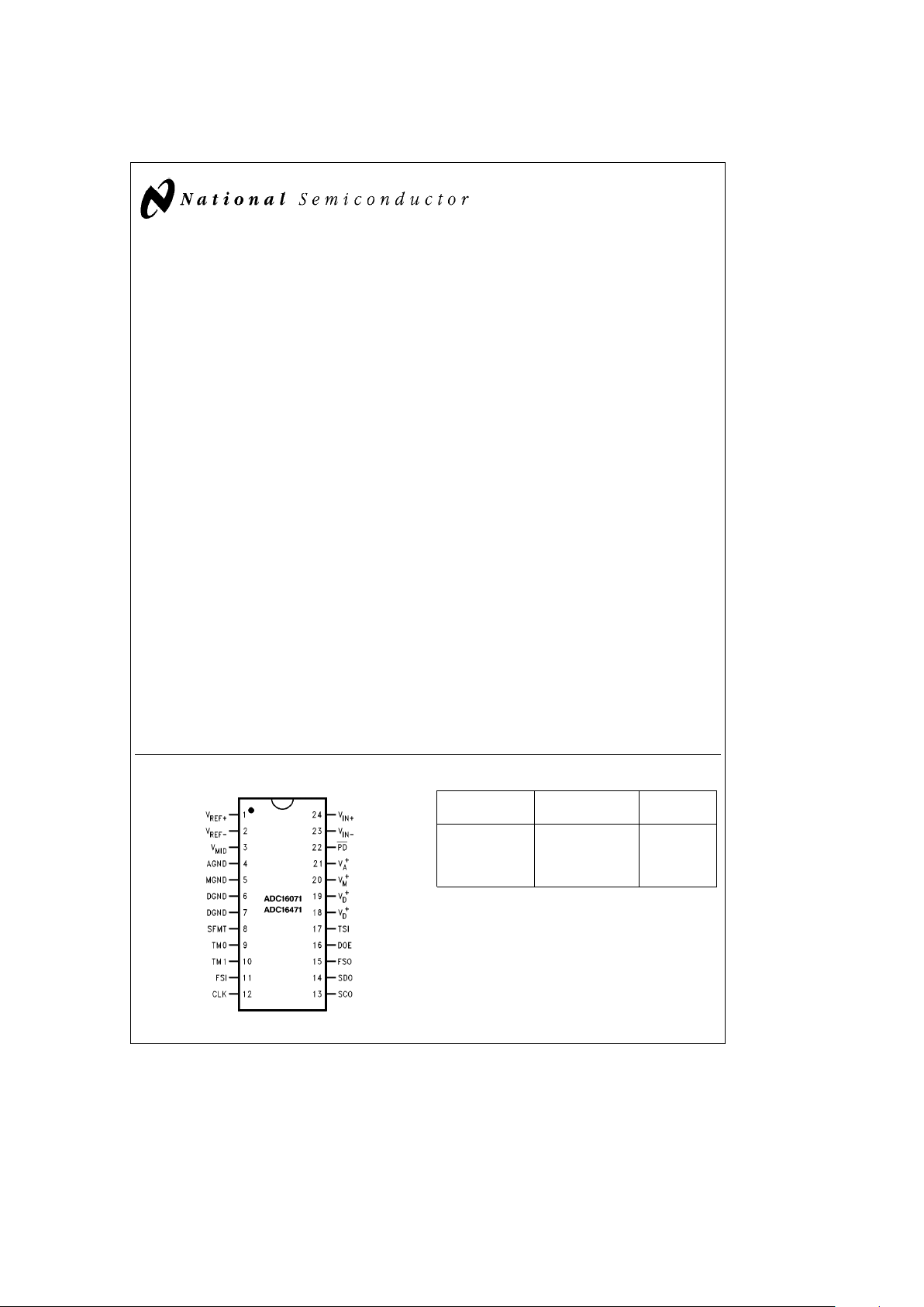
Connection Diagram
TL/H/11454– 2
Ordering Information
Part No. Package
NS Package
No.
ADC16471CIN 24-Pin Molded DIP N24C
ADC16471CIWM 24-Pin SOIC M24B
ADC16071CIN 24-Pin Molded DIP N24C
ADC16071CIWM 24-Pin SOIC M24B
TRI-STATEÉis a registered trademark of National Semiconductor Corporation.
C
1995 National Semiconductor Corporation RRD-B30M75/Printed in U. S. A.
Page 2
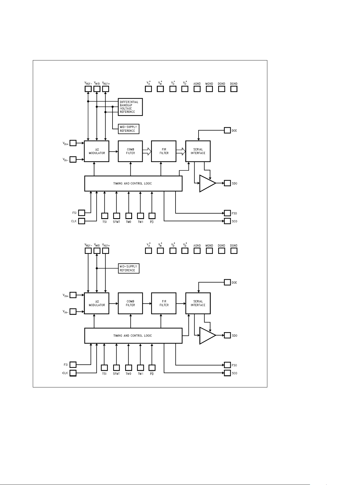
Block Diagram
ADC16471
TL/H/11454– 1
ADC16071
TL/H/11454– 22
2
Page 3
Absolute Maximum Ratings (Notes 1 and 2)
If Military/Aerospace specified devices are required,
please contact the National Semiconductor Sales
Office/Distributors for availability and specifications.
Supply Voltage (V
A
a
,V
D
a
, and V
M
a
)
a
6.5V
Logic Control Inputs
b
0.3V to V
D
a
a
0.3V
Voltage at Other
Inputs and Outputs
b
0.3V to V
A
a
e
V
M
a
a
0.3V
Input Current at Any Pin (Note 3)
g
25 mA
Package Input Current (Note 3)
g
100 mA
Maximum Junction Temperature (Note 4) 150§C
Storage Temperature
b
65§Ctoa150§C
Lead Temperature
N Package (Soldering, 10 sec.) 300
§
C
WM Package (Infrared, 15 sec.) 220
§
C
WM Package (Vapor Phase, 60 sec.) 215
§
C
ESD Susceptibility (Note 5)
Human Body Model 4000V
Machine Model 250V
See AN-450 ‘‘Surface Mounting Methods and Their Effect
on Product Reliability’’ for other methods of soldering surface mount devices.
Operating Ratings (Notes 1 and 2)
Temperature Range
(T
min
s
T
A
s
T
max
)
ADC16471CIN, ADC16071CIN,
b
40§CsT
A
s
a
85§C
ADC16471CIWM, ADC16071CIWM
Supply Voltage
V
A
a
,V
D
a
,V
M
a
4.75V to 5.25V
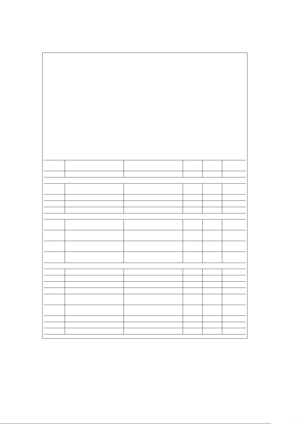
Converter Electrical Characteristics
The following specifications apply for V
M
a
e
V
A
a
e
V
D
a
e
5.0VDC,V
MID
e
V
A
a
/2e2.50V, V
REF
a
e
V
MID
a
1.25V,
V
REF
b
e
V
MID
b
1.25V, f
CLK
e
24.576 MHz, and dynamic tests are performed with an input signal magnitude set atb6dB
with respect to a full-scale input unless otherwise specified. Boldface limits apply for T
A
e
T
J
e
T
min
to T
max
; all other
limits T
A
e
T
J
e
25§C.
Symbol Parameter Conditions
Typical Limits Units
(Note 6) (Note 7) (Limit)
Resolution 16 Bits
f
CLK
e
24.576 MHz (f
s
e
192 kHz)
S/(NaD) Signal-to-NoiseaDistortion Ratio Measurement bandwidthe0.45f
s
76 72 dB (min)
f
IN
e
19 kHz
THD Total Harmonic Distortion f
IN
e
19 kHz 0.010 0.022 % (max)
IMD Intermodulation Distortion f
1
e
18.5 kHz, f
2
e
19.5 kHz 0.010 0.017 % (max)
Converter Noise Floor (Note 8) Measurement Bandwidthe0.45f
s
b
88
b
77 dBFS (min)
f
CLK
e
6.144 MHz (f
s
e
48 kHz)
S/(NaD) Signal-to-NoiseaDistortion Ratio Measurement bandwidthe0.45f
s
85
80 dB (min)
f
IN
e
5 kHz 73 dB (min)
THD Total Harmonic Distortion f
IN
e
5 kHz
0.002
0.0055 % (max)
0.008 % (max)
IMD Intermodulation Distortion f
1
e
4 kHz, f
2
e
5.5 kHz
0.003
0.009 % (max)
0.01 % (max)
Converter Noise Floor (Note 8) Measurement Bandwidthe0.45f
s
b
99
b
92 dBFS (min)
b
89 dBFS (min)
OTHER CONVERTER CHARACTERISTICS
Z
IN
Input Impedance (Note 9) 34 kX
DA
V
Gain Error
g
0.2
g
1.0 %FS (max)
V
OS
Input Offset Voltage 15 mV
I
A
Analog Power Supply Current 23 31 mA (max)
I
M
Modulator Power Supply Current f
CLK
e
24.576 MHz 1.6 2.4
mA (max)
f
CLK
e
6.144 MHz 0.4 0.8
I
D
Digital Power Supply Current f
CLK
e
24.576 MHz 50 65
mA (max)
f
CLK
e
6.144 MHz 13 23
I
SPD
Power-Down Supply Current I
A
a
I
D
a
I
M
0.25 1.3 mA
P
D
Power Dissipation 0.375 0.5 W
V
MID
V
A
a
/2 V
3
Page 4
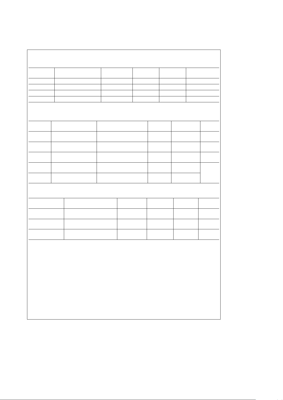
Digital Filter Characteristics
The following specifications apply for V
A
a
e
V
D
a
e
V
M
a
e
5V unless otherwise specified. Boldface limits apply for
T
A
e
T
J
e
T
min
to T
max
; all other limits T
A
e
T
J
e
25§C.
Symbol Parameter Conditions
Typical Limits Units
(Note 6) (Note 7) (Limit)
Stopband Rejection
b
90.0 dB
Passband Ripple
g
0.005 dB
3 dB Cutoff Frequency 0.45 fs
Data Latency 3,968 Clock Cycles
Reference Characteristics (ADC16471 Only)
The following specifications apply for V
A
a
e
V
D
a
e
V
M
a
e
5V, unless otherwise specified. Boldface limits apply for T
A
e
T
J
e
T
min
to T
max
; all other limits T
A
e
T
J
e
25§C.
Symbol Parameter Conditions
Typical Limits Units
(Note 6) (Note 7) (Limit)
V
REF
a
Positive Internal Reference
V
MID
a
1.25
V
MID
a
1.175 V (min)
Output Voltage V
MID
a
1.325 V (max)
V
REF
b
Negative Internal Reference
V
MID
b
1.25
V
MID
b
1.325 V (min)
Output Voltage V
MID
b
1.175 V (max)
D(V
REF
a
– Internal Reference
30 ppm/
§
C
V
REF
b
)/DT Temperature Coefficient
DV
REF
a
/DI Positive Internal Reference Sourcing (0 mAsI
s
a
10 mA)
3.4 6.0
Load Regulation Sinking (
b
1mAsIs0 mA)
mV (max)
DV
REF
b
/DI Negative Internal Reference Sinking (b1mAsIs0 mA)
3.2 6.0
Load Regulation Sourcing (0 mA
sIs
10 mA)
Input Reference Characteristics (ADC16071 Only)
The following specifications apply for V
A
a
e
V
D
a
e
V
M
a
e
5V.
Symbol Parameter Conditions
Typical Limits
Units
(Note 6) (Note 7)
V
REF
a
Positive Reference Voltage 1 V
V
A
a
V
V
REF
b
Negative Reference Voltage 0 V
V
A
ab
1V
V
REF
a
–V
REF
b
Total Reference Voltage 1 V
V
A
a
V
4
Page 5
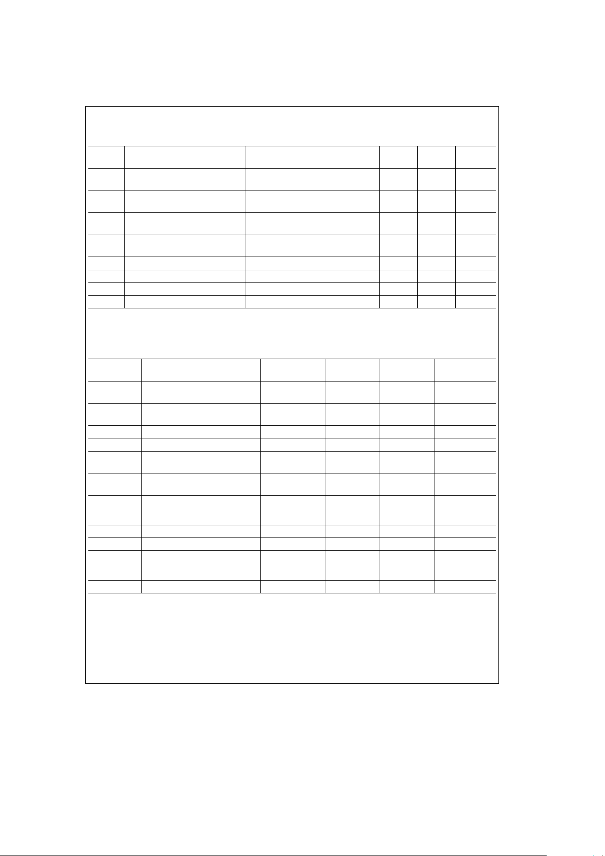
DC Electrical Characteristics
The following specifications apply for V
A
a
e
V
D
a
e
V
M
a
e
5V unless otherwise specified. Boldface limits apply for T
A
e
T
J
e
T
MIN
to T
MAX
; all other limits T
A
e
T
J
e
25§C.
Symbol Parameter Conditions
Typical Limits Units
(Note 6) (Note 7) (Limit)
V
IH
Logic High Input Voltage V
D
a
e
5.25V V
D
a
V (max)
2.3 V (min)
V
IL
Logic Low Input Voltage V
D
a
e
4.75V 0.8 V (max)
b
0.3 V (min)
V
OH
Logic High Output Voltage Logic High Output Currenteb400 mA,
2.4 V (min)
V
D
a
e
4.75V
V
OL
Logic Low Output Voltage Logic Low Output Currente2 mA,
0.5 V (max)
V
D
a
e
5.25V
I
IN(1)
Logical ‘‘1’’ Input Current 1.0 5.0 mA (max)
I
IN(0)
Logical ‘‘0’’ Input Current
b
1.0
b
5.0 mA (max)
I
TSI
SDO TRI-STATEÉLeakage Current V
IN
e
0.4V to 2.4V 1.0 5.0 mA (max)
C
IN
Logic Input Capacitance V
IN
e
0toV
D
a
5pF
AC Electrical Characteristics for Clock In (CLK), Serial Clock Out (SCO), and
Frame Sync In (FSI)
The following specifications apply for V
A
a
e
V
D
a
e
V
M
a
e
5V unless otherwise specified. Boldface limits apply for T
A
e
T
J
e
T
MIN
to T
MAX
; all other limits T
A
e
T
J
e
25§C.
Symbol Parameter Conditions
Typical Limits Units
(Note 6) (Note 7) (Limit)
f
CLK
CLK Frequency Range 25 MHz (max)
(f
CLK
e
1/t
CLK
) 1 MHz (min)
t
CLK
CLK Period 1000 ns (max)
(t
CLK
e
1/f
CLK
) 40 ns (min)
t
CLKL
CLK Low Pulse Width 16 ns (min)
t
CLKH
CLK High Pulse Width 14 ns (min)
t
R
CLK Rise Time 10 ns (max)
3 ns (min)
t
F
CLK Fall Time 10 ns (max)
3 ns (min)
t
FSILOW
Minimum Frame Sync Input
2t
CLK
(min)Low Time before Frame Sync
Input Asserted High
t
FSISU
Frame Sync Input Setup Time 10 ns (min)
t
FSIH
Frame Sync Input Hold Time 10 ns (min)
t
SCOD
Serial Clock Output Delay
20 ns (max)
Time from Rising Edge
12
5 ns (min)
of CLK
t
SCO
Serial Clock Output Period 4 t
CLK
5
Page 6
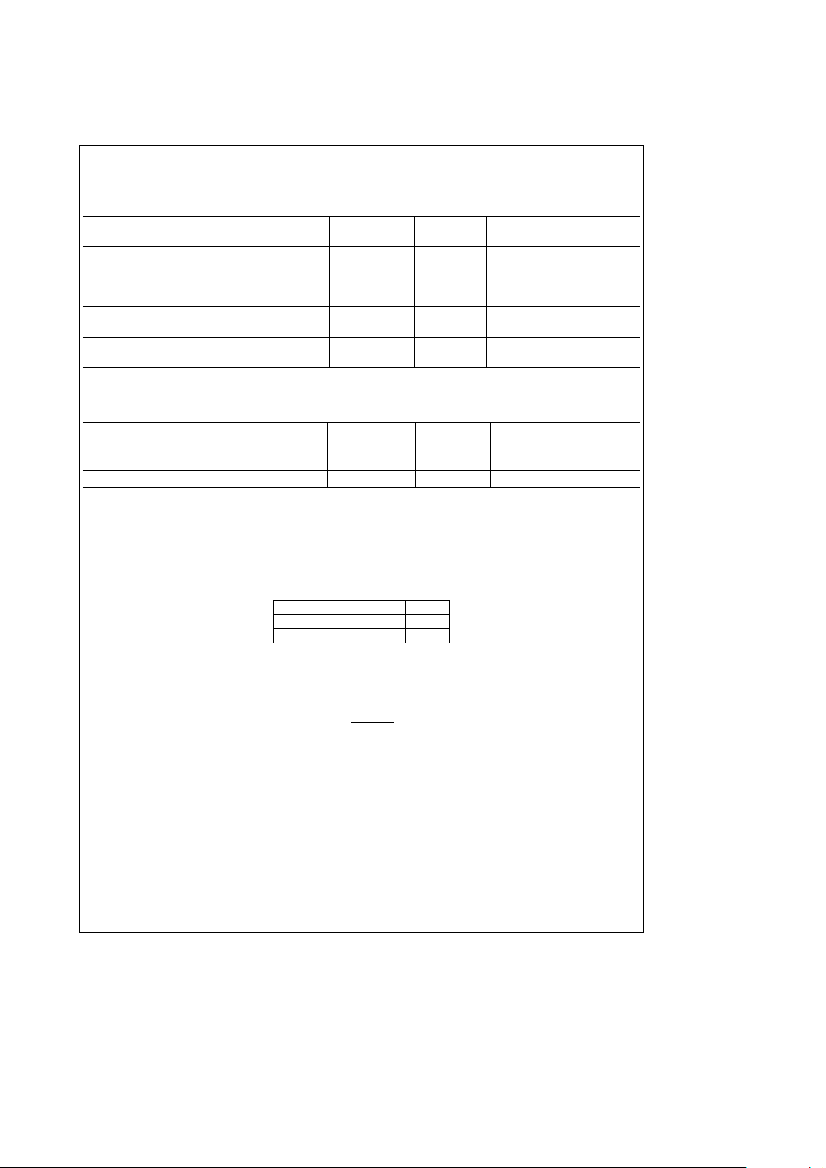
AC Electrical Characteristics for Frame Sync Out (FSO), Serial Clock Out
(SCO), and Serial Data Out (SDO)
The following specifications apply for V
A
a
e
V
D
a
e
V
M
a
e
5V unless otherwise specified. Boldface limits apply for T
A
e
T
J
e
T
MIN
to T
MAX
; all other limits T
A
e
T
J
e
25§C.
Symbol Parameter Conditions
Typical Limits Units
(Note 6) (Note 7) (Limit)
t
SCOFSOH
Delay from Serial Clock Out to
2 5 ns (max)
Frame Sync Output High
t
SCOFSOL
Delay from Serial Clock Out to
2 5 ns (max)
Frame Sync Output Low
t
SDOV
Delay from Serial Clock Out to
3 8 ns (max)
Serial Data Output Valid
t
FSIFSOL
Delay from Frame Sync Input to
8 t
CLK
(max)
Frame Sync Output Low
AC Electrical Characteristics for Data Output Enable (DOE)
The following specifications apply for V
A
a
e
V
D
a
e
V
M
a
e
5V unless otherwise specified. Boldface limits apply for T
A
e
T
J
e
T
MIN
to T
MAX
; all other limits T
A
e
T
J
e
25§C.
Symbol Parameter Conditions
Typical Limits Units
(Note 6) (Note 7) (Limit)
t
DOEE
Data Output Enable Delay Time 20 25 ns (max)
t
DOED
Data Output Disable Delay Time 16 20 ns (max)
Note 1: Absolute Maximum Ratings indicate limits beyond which damage to the device may occur. Operating Ratings indicate conditions for which the device is
functional, but do not guarantee specific performance limits. For guaranteed specifications and test conditions, see the Electrical Characteristics. The guaranteed
specifications apply for the test conditions listed. Some performance characteristics may degrade when the device is not operated under the listed test conditions.
Note 2: All voltages are measured with respect to GND, unless otherwise specified.
Note 3: When the input voltage (V
IN
) at any pin exceeds the power supply rails (V
IN
k
GND or V
IN
l
(V
A
a
,V
M
a
,orV
D
a
)), the current at that pin should be limited
to 25 mA. The 100 mA maximum package input current rating allows the voltage at any four pins, with an input current of 25 mA each, to simultaneously exceed the
power supply voltages.
Note 4: The maximum power dissipation is a function of the maximum junction temperature (T
J(MAX)
), total thermal resistance (iJA), and ambient temperature (TA).
The maximum allowable power dissipation at any ambient temperature is P
D(max)
e
(T
J(max)
b
TA)/iJA. When board mounted, the ADC16071/ADC16471’s
typical thermal resistance is:
Order Number i
JA
ADC16071CIN, ADC16471CIN 47§C/W
ADC16071CIWM, ADC16471CIWM 72§C/W
Note 5: Human body model, 100 pF discharge through a 1.5 kX resistor. The machine model is a 200 pF capacitor discharged directly into each pin.
Note 6: Typicals are at T
A
e
25§C and represent most likely parametric norm.
Note 7: Limits are guaranteed to National’s AOQL (Average Output Quality Level).
Note 8: The V
IN
a
pin is shorted to the V
IN
b
pin.
Note 9: The input impedance between V
IN
a
and V
IN
b
due to the effective resistance of the switch capacitor input varies as follows:
Z
IN
e
10
12
2.35* (
f
CLK
2
)
6
Page 7

Typical Performance Characteristics
S/(NaD) vs VINAmplitude Data Rate (fs)
S/(N
a
D) vs Output
S/(N
a
D) vs Temperature
f
IN
e
20 kHz
f
s
e
192 kHz,
Spectral Response,
f
IN
e
80 kHz
f
s
e
192 kHz,
Spectral Response,
f
IN
e
5 kHz
f
s
e
48 kHz,
Spectral Response,
(I
A
a
IM) vs Temperature
Analog Supply Current
IDvs Temperature
Digital Supply Current
Data Rate (fs)
(I
A
a
IM) vs Output
Analog Supply Current
Rate (fs)
(I
D
) vs Output Data
Digital Supply Current
Digital Filter
Frequency Response of
TL/H/11454– 24
7
Page 8

TL/H/11454– 8
FIGURE 1. Timing Diagrams for Clock Input (CLK),
Frame Sync Input (FSI), and Serial Clock Output (SCO)
8
Page 9

TL/H/11454– 4
FIGURE 2. Detailed Timing Diagrams for Frame Sync Input (FSI), Frame Sync Out (FSO), Serial Clock Out (SCO), and Serial Data Out (SDO)
9
Page 10

TL/H/11454– 5
FIGURE 3. Timing Diagrams for Frame Sync Out (FSO), Serial Clock Out (SCO), and Serial Data Out (SDO)
10
Page 11

TL/H/11454– 6
FIGURE 4. Master/Slave Mode Timing Diagrams
11
Page 12

TL/H/11454– 7
FIGURE 5. Timing Diagrams for Data Output Enable (DOE) and Serial Data Out (SDO)
Pin Description
V
REF
a
,V
REF
b
These are the ADC16471’s internal differential reference’s bypass pins. Their nominal output voltage is
g
1.25V centered
around the voltage at the V
MID
pin, typically
V
A
a
/2. V
REF
a
,V
MID
, and V
REF
b
should
be bypassed with a parallel combination of
10 mF and 0.1 mF capacitors. For the
ADC16071, these are the reference voltage
inputs. V
REF
a
and V
MID
should be bypassed with a parallel combination of 10 mF
and 0.1 mF capacitors.
V
MID
This pin is the internal differential reference’s V
A
a
/2 output pin. V
MID
should be
bypassed with a parallel combination of
10 mF and 0.1 mF capacitors.
V
IN
a
,V
IN
b
These are the ADC’s differential input pins.
Signals applied to these pins can be singleended or differential with respect to the
V
MID
voltage.
PD This is the input pin used to activate the
power-down mode. When a logic LOW (0)
is applied to this pin the supply current
drops from 100 mA (max) to 1.3 mA (max).
AGND This is the connection to system analog
ground. Internally, this ground is connected
to the analog circuitry, including the fourthorder modulator.
DGND This is the connection to system digital
ground. Internally, this ground is connected
to all digital circuitry except the modulator’s
clock.
MGND This is the ground pin for the modulator’s
clock. It should be connected to analog
ground through its own connection that is
separate from that used by AGND.
V
A
a
This pin is the connection to the system analog voltage supply. Best performance is
achieved when this pin is bypassed with a
parallel combination of 10 mF and 0.1 mF
capacitors.
V
M
a
This is the modulator’s supply pin. V
M
a
should
be connected to the system analog voltage
supply with a circuit board trace or connection
that is separate from that used to supply V
A
a
.
Best performance is achieved when this pin is
bypassed with a parallel combination of 10 mF
and 0.1 mF capacitors.
V
D
a
This pin is the connection to the system digital
voltage supply. Best performance is achieved
when this pin is bypassed with a parallel combination of 10 mF and 0.1 mF capacitors.
SFMT This is the Serial Format pin. The logic level
applied to the SFMT pin determines whether
conversion data shifted out of the SDO pin is
valid on the rising or falling edge of SCO. It also
controls the format of the Frame Sync Out
(FSO) signal. See the Serial Interface section
for details.
TM0, TM1 Used to enabled test mode during production.
Connect both pins to DGND.
FSI This is the Frame Sync Input pin. FSI is an
input used to synchronize the ADC16071/
ADC16471’s conversions to an external source.
The state of FSI is sampled on the falling edge
of CLK. See the Serial Interface section for
details.
CLK This is the clock signal input pin. The signal ap-
plied to this pin sets the sample rate of the
ADC16071/ADC16471’s modulator to f
CLK
/2.
The frequency range can be 1 MHz
s
f
CLK
s
25 MHz.
SCO This is the Serial Clock Output pin. The
ADC16071/ADC16471’s serial data transmission is synchronous with the SCO signal. SCO
has a frequency of f
CLK
/4. See the Serial In-
terface section for details.
SDO This is the Serial Data Output pin. The
ADC16071/ADC16471’s conversion data is
shifted out from this pin synchronous to the
SCO signal. See the Serial Interface section
for details.
12
Page 13

Pin Description (Continued)
FSO This is the Frame Sync Output pin. FSO is used
to synchronize an external device to the
ADC16071/ADC16471’s 32 SCO cycle data
transmission frame. The format of the signal on
FSO depends on the logic level applied to the
SFMT pin. See the Serial Interface section for
details.
TSI This is the Time Slot Input pin. TSI can be used
to allow two ADC16071/ADC16471’s to share a
single serial data line. The logic level applied to
TSI controls the active state of the ADC16071/
ADC16471’s DOE pin. See the Serial Interface
and the Two Channel Multiplexed Operation
sections for details.
DOE This is the Data Output Enable pin. DOE is used
to control SDO’s TRI-STATE output buffer. The
active state of DOE is controlled by the logic level applied to the TSI pin. See the Serial Inter-
face and the Two Channel Multiplexed Operation sections for details.
Applications Information
TYPICAL PERFORMANCE RESULTS
Figure 6
shows a 16k point FFT plot of the baseband output
spectrum during conversion of a 24 kHz input signal.
CLOCK GENERATION
The ADC16071/ADC16471 requires a sampling-clock signal that is free of ringing (over/undershoot of no more than
100 mV
p-p
) and has a rise and fall time in the range of 3 ns–
10 ns. We have tested and recommended crystal clock oscillators from Ecliptek (EC1100 series) and SaRonix
(NCH060 and NCH080 series). Both of these families use
HCMOS logic circuitry for very fast rise and fall times.
TL/H/11454– 13
FIGURE 6. Typical Performance of the ADC16071/ADC16471 at f
S
e
192 kHz, f
IN
e
24 kHz
13
Page 14

Applications Information (Continued)
Overshoot and ringing can be reduced by adding a series
damping resistor between the crystal oscillator’s output (pin
8) and the ADC16071/ADC16471’s CLK (pin 12), as shown
in
Figure 7.
The actual resistor value is dependent on the
board layout and trace length that connects the oscillator or
CLK source to the ADC. A typical starting value is 50X with
a range of 27X to 150X.
TL/H/11454– 23
FIGURE 7. Damping Resistor Reduces
Clock Signal Overshoot
SERIAL INTERFACE
The ADC16071 and the ADC16471 have three serial interface output pins: Serial Data Output (SDO), Frame Sync
Output (FSO), and Serial Clock Output (SCO). SCO has a
frequency of f
CLK
/4. Each of the ADC16071/ADC16471’s
16-bit conversions is transmitted within the first half of the
data transmission frame. A data transmission frame is 32
SCO cycles in duration. Two’s complement data shifts out
on the SDO pin beginning with bit 15 (MSB) and ending with
bit 0 (LSB), taking 16 SCO cycles. SDO then shifts out
zeroes for the next 16 SCO cycles to maintain compatibility
with two channel multiplexed operation.
The serial data that is shifted out of the SDO pin is synchronous with SCO. Depending on the logic level applied to the
Serial Format pin (SFMT), the data on the SDO pin is valid
on either the falling or rising edge of SCO. If a logic Low is
applied to SFMT, then the data on SDO is valid on the falling edge of SCO. If a logic High is applied to SFMT, then
the data on SDO is valid on the rising edge of SCO. See
Figure 2
.
The FSO signal is used to synchronize other devices to the
ADC16071/ADC16471’s data transmission frame. Depending on the logic level applied to SFMT, the signal on FSO is
either a short pulse (approximately one SCO cycle in duration) ending just before the transmission of bit 15 on SDO,
or a square wave with a period of 32 SCO cycles going low
just before the transmission of bit 15 and going high just
after the transmission of bit 0. If a logic Low is applied to
SFMT, FSO will be high for approximately one SCO cycle
and fall low just before the transmission of bit 15 and stay
low for the remainder of the transmission frame. If a logic
High is applied to SFMT, FSO will be low during the transmission of bits 15 – 0 and high during the next 16 SCO cycles. See
Figure 3
.
The Frame Sync Input (FSI), is used to synchronize the
ADC16071/ADC16471’s conversions to an external source.
The logic state of FSI is captured by the ADC16071/
ADC16471 on the falling edge of CLK.IfanFSI low to high
transition is sensed between adjacent CLK falling edges,
the ADC16071/ADC16471 will interrupt its current data
transmission frame and begin a new one. See
Figure 4
.
Due to the data latency of the ADC16071/ADC16471’s digital filters, the first 31 conversions following a frame sync
input signal will represent inaccurate data, unless the frame
syncs are applied at constant 32 SCO cycle intervals. If no
FSI signal is applied (FSI is kept High or Low), the
ADC16071/ADC16471 will internally create a frame sync
every 32 SCO cycles.
The Data Output Enable pin (DOE), is used to enable and
disable the output of data on SDO. When DOE is deactivated, SDO stops driving the serial data line by entering a high
impedance TRI-STATE. DOE’s active state matches the
logic level applied to the Time Slot Input pin (TSI). If a logic
Low is applied to TSI, the ADC16071/ADC16471’s SDO pin
will shift out data when DOE is Low, and be in a high impedance TRI-STATE when DOE is High. If a logic High is applied to TSI, SDO will shift out data when DOE is High, and
be in a high impedance TRI-STATE when DOE is Low.
TWO CHANNEL MULTIPLEXED OPERATION
Two ADC16071/ADC16471’s can easily be configured to
share a single serial data line and operate in a ‘‘stereo’’, or
two channel multiplexed mode. They share the serial data
bus by alternating transmission of conversion data on their
respective SDO pins. One of the ADC16071/ADC16471’s,
the Master, shifts its conversion data out of SDO during the
first 16 SCO cycles of the data transmission frame. The
other ADC16071/ADC16471, the Slave, shifts its data out
during the second 16 SCO cycles of the data transmission
frame.
The Slave is selected by applying a logic High to its TSI pin
and a logic High to its SFMT pin. The Master is chosen by
applying a logic Low to its TSI pin and a logic High to its
SFMT pin. As shown in
Figure 8
, the Master’s FSO is used
to control the DOE of both the Master and the Slave as well
as to synchronize the two ADC16071/ADC16471’s by driving the Slave’s Frame Sync Input pin, FSI. As the Master
finishes transmitting its 16 bits of conversion data, its FSO
goes High. This triggers the Slave’s FSI, causing the Slave
to begin transmitting its 16 bits of conversion data.
The Master’s DOE is active Low and the Slave’s DOE is
active High. Since the same signal, the Master’s FSO,is
connected to both of the converters’ DOE pins, one converter will shift out data on its SDO pin while the other is in
TRI-STATE, allowing the two ADC16071/ADC16471’s to
share the same serial data transmission line.
POWER SUPPLY AND GROUNDING
The ADC16071/ADC16471 has on-chip 50 pF bypass capacitors between the supply-pin bonding pads and their corresponding grounds. There are 24 of these capacitors, 6 for
the analog section and 18 for the digital, resulting in a total
value of 1200 pF. They help control ringing on the on-chip
power supply busses, especially in the digital section. Further, they help enhance the baseband noise performance of
the analog modulator.
14
Page 15

Applications Information (Continued)
TL/H/11454– 14
FIGURE 8. Two Channel Multiplexed Operation Connection Diagram
Best converter performance is achieved when these internal bypass capacitors are supplemented with additional external power-supply decoupling capacitors. This ensures the
lowest ac-bypass impedance path for the ADC16071/
ADC16471’s dynamic current requirements. Each of the
ADC16071/ADC16471’s four supply pins should be individually bypassed, using a parallel combination of 10 mF (tantalum) and 0.1 mF (monolithic ceramic), to its corresponding
ground pin:
V
A
a
(Pin 21)xAGND (Pin 4)
V
M
a
(Pin 20)xMGND (Pin 5)
V
D
a
(Pin 19)xDGND (Pin 6)
V
D
a
(Pin 18)xDGND (Pin 7)
Short lead lengths are mandatory. Therefore, surface mount
capacitors are
strongly
recommended.
POWER SUPPLY VOLTAGES FOR BEST
PERFORMANCE
While adequate performance will be achieved by operating
the ADC16071/ADC16471 with
a
5V connected to V
A
a
,
V
M
a
and V
D
a
, dynamic performance, as measured by
S/(N
a
D), can be further enhanced by slightly raising the
analog supply voltage and lowering the digital supply voltage.
ANALOG INPUT
The ADC16071 and the ADC16471 generate a two’s complement output determined by the following equation:
Output Code
e
(V
IN
ab
V
IN
b
) (32768)
(V
REF
ab
V
REF
b
)
Round off to the nearest integer value betweenb32768
and 32767.
The signals applied to V
IN
a
and V
IN
b
must be between
V
A
a
and analog ground. For accurate conversions, the ab-
solute difference between V
IN
a
and V
IN
b
should be less
than the difference between V
REF
a
and V
REF
b
. Best harmonic performance will result when a differential voltage is
applied to V
IN
a
and V
IN
b
that has a common mode voltage
at or below V
MID
.
Due to overloading in the ADC16071/ADC16471’s DR modulator, performance degrades considerably as the input amplitude approaches full scale. With an input that peaks at
b
2 dB from full scale, S/(NaD) is about 2 dB worse than
with a
b
6 dB input. With ab1 dB input, S/(NaD) can be
10 dB worse than with a
b
6 dB input.
15
Page 16

Applications Information (Continued)
ANALOG SIGNAL CONDITIONING
The ADC16071/ADC16471’s digital comb and FIR filter
combine to create the band-limiting anti-aliasing filter, generating a steep cutoff at the upper range of the sampled
baseband. Additional external filtering is needed to ensure
that the best conversion performance is maintained. The
external filtering uses a simple R-C lowpass filter. A suggested circuit is shown in
Figure 9.
The values of R1,R2,C1,
C
2
, and C3are found using the following equation:
f
c(b3 dB)
e
1
6q
RC
where ReR
1
e
R2and CeC
1
e
C
2
e
C3.
The effects of the external filter are minimized by choosing
a minimum cutoff frequency equal to f
CLK
/32. As an exam-
ple, for f
CLK
equal to 6.144 MHz, set R
1
e
R
2
e
82.5X and
C
1
e
C
2
e
C
3
e
3300 pF. This sets the input network’s
cutoff frequency at 194 kHz. For f
CLK
equal to 24.576 MHz,
set R
1
e
R
2
e
20X and C
1
e
C
2
e
C
3
e
3300 pF. This
sets the input network’s cutoff frequency at 803 kHz.
RELATION BETWEEN CAPACITOR DIELECTRIC AND
SIGNAL DISTORTION
For any capacitors connected to the ADC16071/
ADC16471’s analog inputs, the dielectric plays an important
role in determining the amount of distortion generated in the
input signal. The capacitors used must have low dielectric
absorption. This requirement is fulfilled using capacitors that
have film dielectrics. Of these, polypropylene and polystyrene are the best. These are followed by polycarbonate and
mylar. If ceramic capacitors are chosen, use only capacitors
with NPO dielectrics.
INTERNAL DIFFERENTIAL BANDGAP REFERENCE
A fully differential bandgap reference generates local feedback voltages, V
REF
a
and V
REF
b
, for the analog modulator. The outputs of this reference are trimmed to be equal to
V
MID
plus or minus 1.25V. This gives a differential reference
voltage of 2.5V which results in a
g
2.5V differential input
range. The ADC16071 does not have the internal differential bandgap reference, allowing the user the flexibility to
determine the full scale range by using an external voltage
reference.
EXTERNAL VOLTAGE REFERENCE FOR THE
ADC16071
Figure 10
shows the suggested connection diagram for the
ADC16071. The LM4041-ADJ is set to 2.0V and is applied
to the ADC16071’s V
REF
a
input.
The reference voltage must be free of noise. This is accomplished using the same capacitor combination used with the
ADC16471’s reference pins with the exception of V
REF
b
,
which is connected to analog ground.
Figures 11
and12show the suggested circuits for ac-cou-
pled applications.
TL/H/11454– 15
Suggested values:
R
1
e
R
2
e
20X, 5%, metal film
C
1
e
C
2
e
C
3
e
3300 pF, 5%,
polypropylene
*Parallel combination of 10 mF tan-
talum and a 0.1 m F monolithic ceramic capacitors.
FIGURE 9. Typical Connection Diagram for the ADC16471
16
Page 17

Applications Information (Continued)
TL/H/11454– 16
Suggested values:
R
1
e
R
2
e
20X, 5%, metal film
C
1
e
C
2
e
C
3
e
3300 pF, 5%,
polypropylene
*Parallel combination of 10 mF tan-
talum and a 0.1 m F monolithic ceramic capacitors.
FIGURE 10. Typical Connection Diagram for the ADC16071
TL/H/11454– 17
Suggested values:
R
1
e
R
2
e
20X, 5%, metal film
C
1
e
C
2
e
C
3
e
3300 pF, 5%,
polypropylene
*Parallel combination of 10 mF tan-
talum and a 0.1 m F monolithic ceramic capacitors.
FIGURE 11. Typical Connection Diagram for the ADC16471 with AC-Coupled Inputs
TL/H/11454– 18
Suggested values:
R
1
e
R
2
e
20X, 5%, metal film
C
1
e
C
2
e
C
3
e
3300 pF, 5%,
polypropylene
*Parallel combination of 10 mF tan-
talum and a 0.1 m F monolithic ceramic capacitors.
FIGURE 12. Typical Connection Diagram for the ADC16071 with AC-Coupled Inputs
17
Page 18

Applications Information (Continued)
DSP INTERFACES
The ADC16071/ADC16471 was designed to connect to popular DSPs without intervening ‘‘glue logic’’.
Figures 13, 14,
and
15
show suggested connection schematics for the DSP56001, TMS320C3x, and the ADSP-2101 families.
TL/H/11454– 19
FIGURE 13. Interface Connections between the ADC16071/ADC16471 and the Motorola DSP56001
TL/H/11454– 20
FIGURE 14. Interface Connections between the ADC16071/ADC16471 and the Texas Instruments TMS320C3x
TL/H/11454– 21
FIGURE 15. Interface Connections between the ADC16071/ADC16471 and the Analog Devices ADSP-2101
18
Page 19

Physical Dimensions inches (millimeters)
24-Lead (0.300×Wide) Molded Small Outline Package, JEDEC
Order Number ADC16071CIWM or ADC16471CIWM
NS Package Number M24B
19
Page 20

ADC16071/ADC16471 16-Bit Delta-Sigma 192 ks/s Analog-to-Digital Converters
Physical Dimensions inches (millimeters) (Continued)
24-Lead (0.300×Wide) Molded Dual-In-Line Package
Order Number ADC16071CIN or ADC16471CIN
NS Package Number N24C
LIFE SUPPORT POLICY
NATIONAL’S PRODUCTS ARE NOT AUTHORIZED FOR USE AS CRITICAL COMPONENTS IN LIFE SUPPORT
DEVICES OR SYSTEMS WITHOUT THE EXPRESS WRITTEN APPROVAL OF THE PRESIDENT OF NATIONAL
SEMICONDUCTOR CORPORATION. As used herein:
1. Life support devices or systems are devices or 2. A critical component is any component of a life
systems which, (a) are intended for surgical implant support device or system whose failure to perform can
into the body, or (b) support or sustain life, and whose be reasonably expected to cause the failure of the life
failure to perform, when properly used in accordance support device or system, or to affect its safety or
with instructions for use provided in the labeling, can effectiveness.
be reasonably expected to result in a significant injury
to the user.
National Semiconductor National Semiconductor National Semiconductor National Semiconductor National Semiconductores National Semiconductor
Corporation GmbH Japan Ltd. Hong Kong Ltd. Do Brazil Ltda. (Australia) Pty, Ltd.
2900 Semiconductor Drive Livry-Gargan-Str. 10 Sumitomo Chemical 13th Floor, Straight Block, Rue Deputado Lacorda Franco Building 16
P.O. Box 58090 D-82256 F4urstenfeldbruck Engineering Center Ocean Centre, 5 Canton Rd. 120-3A Business Park Drive
Santa Clara, CA 95052-8090 Germany Bldg. 7F Tsimshatsui, Kowloon Sao Paulo-SP Monash Business Park
Tel: 1(800) 272-9959 Tel: (81-41) 35-0 1-7-1, Nakase, Mihama-Ku Hong Kong Brazil 05418-000 Nottinghill, Melbourne
TWX: (910) 339-9240 Telex: 527649 Chiba-City, Tel: (852) 2737-1600 Tel: (55-11) 212-5066 Victoria 3168 Australia
Fax: (81-41) 35-1 Ciba Prefecture 261 Fax: (852) 2736-9960 Telex: 391-1131931 NSBR BR Tel: (3) 558-9999
Tel: (043) 299-2300 Fax: (55-11) 212-1181 Fax: (3) 558-9998
Fax: (043) 299-2500
National does not assume any responsibility for use of any circuitry described, no circuit patent licenses are implied and National reserves the right at any time without notice to change said circuitry and specifications.
 Loading...