

Page 1
January 2000
ADC16061
Self-Calibrating 16-Bit, 2.5 MSPS, 390 mW A/D Converter
ADC16061 Self-Calibrating 16-Bit, 2.5 MSPS, 390 mW A/D Converter
General Description
The ADC16061 is a self-calibrating 16-bit, 2.5 Megasample
per secondanalog to digital converter. It operates on a single
+5V supply, consuming just 390mW (typical).
The ADC16061 provides an easy and affordable upgrade
from 12 bit and 14 bit converters. The ADC16061 may also
be used to replace many hybrid converters with a resultant
saving of space, power and cost.
The ADC16061 operates with excellent dynamic performance at input frequencies up to
calibration feature of theADC16061 can be used to get more
consistent and repeatable results over the entire operating
temperature range. On-command self-calibration reduces
many of the effects of temperature-induced drift, resulting in
more repeatable conversions.
The Power Down feature reduces power consumption to
less than 2mW.
TheADC16061 comes in aTQFP and is designed to operate
over the commercial temperature range of 0˚C to +70˚C.
1
⁄2the clock frequency.The
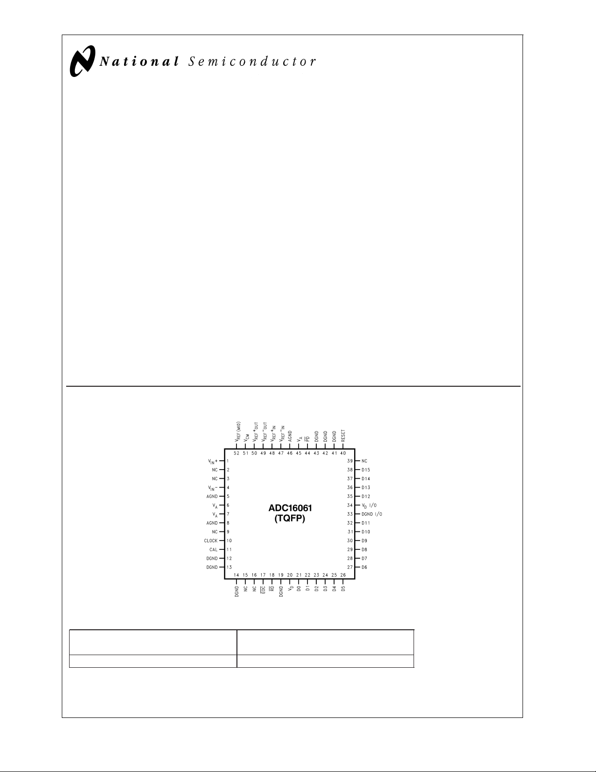
Connection Diagram
Features
n Single +5V Operation
n Self Calibration
n Power Down Mode
Key Specifications
n Resolution 16 Bits
n Conversion Rate 2.5 Msps (min)
n DNL 1.0 LSB (typ)
n SNR (f
n Supply Voltage +5V
n Power Consumption 390mW (typ)
= 500 kHz) 80 dB (typ)
IN
±
Applications
n PC-Based Data Acquisition
n Document Scanners
n Digital Copiers
n Film Scanners
n Blood Analyzers
n Sonar/Radar
%
5
DS100889-1
Ordering Information
Commercial
(0˚C ≤ TA ≤ +70˚C)
ADC16061CCVT VEG52A 52 Pin Thin Quad Flat Pack
© 2000 National Semiconductor Corporation DS100889 www.national.com
Package
Page 2
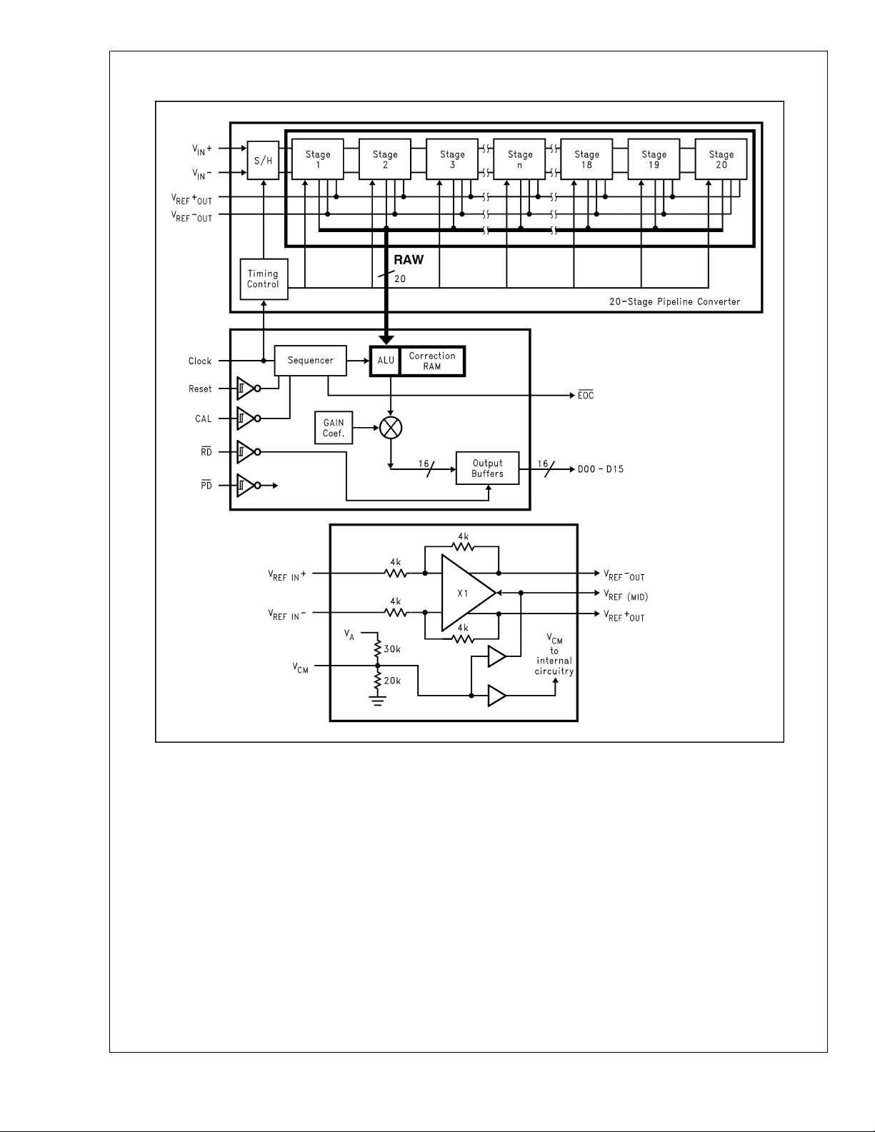
Block Diagram
ADC16061
www.national.com 2
DS100889-2
Page 3
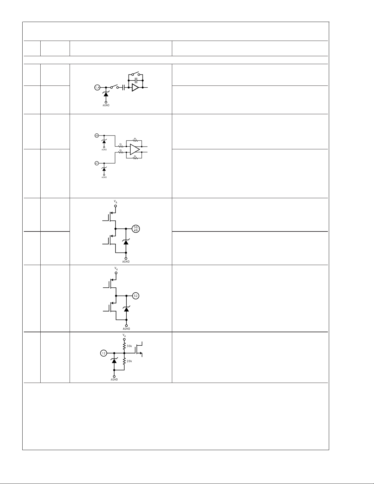
Pin Descriptions and Equivalent Circuits
ADC16061
Pin
Symbol Equivalent Circuit
No.
Analog I/O
1V
4V
48 V
47 V
50 V
IN
IN
REF+IN
REF−IN
REF+OUT
Description
Non-Inverting analog signal Input. With a 2.0V reference voltage
+
and a 2.0V common mode voltage, V
, the input signal voltage
CM
range is from 1.0 volt to 3.0 Volts.
Inverting analog signal Input. With a 2.0V reference voltage and a
−
2.0V common mode voltage, V
from 1.0 Volt to 3.0 Volts. The input signal should be balanced for
, the input signal voltage range is
CM
best performance.
Positive reference input. This pin should be bypassed to AGND
with a 0.1 µF monolithic capacitor.
+ minus V
V
REF
maximum of 2.2V. The full-scale input voltage is equal to V
minus V
REF−IN
should be a minimum of 1.8V and a
REF− IN
.
REF+IN
Negative reference input. In most applications this pin should be
connected to AGND and the full reference voltage applied to
V
REF+IN
. If the application requires that V
REF−IN
be offset from
AGND, this pin should be bypassed to AGND with a 0.1 µF
monolithic capacitor. V
REF+IN
minus V
REF− IN
should be a
minimum of 1.8V and a maximum of 2.2V. The full-scale input
voltage is equal to V
REF+IN
minus V
REF−IN
.
Output of the high impedance positive reference buffer. With a
2.0V reference input, and with a V
of 2.0V, this pin will have a
CM
3.0V output voltage. This pin should be bypassed to AGND with a
0.1 µF monolithic capacitor in parallel with a 10 µF capacitor.
49 V
REF−OUT
52 V
REF (MID)
51 V
CM
The output of the negative reference buffer. With a 2.0V reference
andaV
of 2.0V, this pin will have a 1.0V output voltage. This
CM
pin should be bypassed to AGND with a 0.1 µF monolithic
capacitor in parallel with a 10 µF capacitor.
Output of the reference mid-point, nominally equal to 0.4 V
A
(2.0V). This pin should be bypassed to AGND with a 0.1 µF
monolithic capacitor. This voltage is derived from V
CM
.
Input to the common mode buffer, nominally equal to 40%of the
supply voltage (2.0V). This pin should be bypassed to AGND with
a 0.1 µF monolithic capacitor. Best performance is obtained if this
pin is driven with a low impedance source of 2.0V.
www.national.com3
Page 4
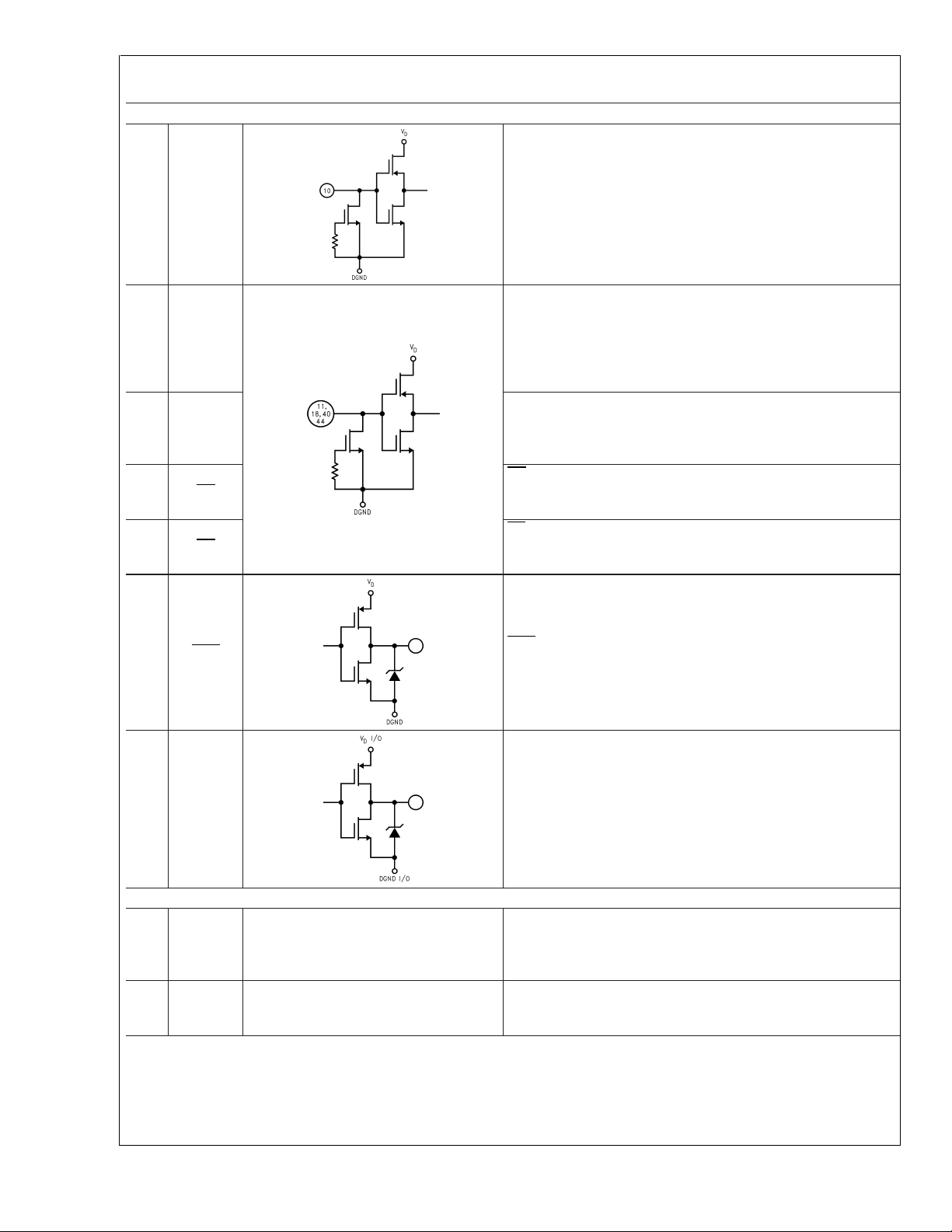
Pin Descriptions and Equivalent Circuits (Continued)
Digital I/O
ADC16061
Digital clock input. The input voltage is captured tADafter the fall of
10 CLOCK
11 CAL
40 RESET
18 RD
44 PD
the clock signal. The range of frequencies for this input is 300 kHz
to 2.5 MHz. The clock frequency should not be changed or
interrupted during conversion or while reading data output.
CAL is a level-sensitive digital input that, when pulsed high for at
least two clock cycles, puts the ADC into the CALIBRATE mode.
Calibration should be performed upon ADC power-up (after
asserting a reset) and each time the temperature changes by more
than 50˚C since the ADC16061 was last calibrated. See Section
2.3 for more information.
RESET is a level-sensitive digital input that, when pulsed high for
at least 2 CLOCK cycles, results in the resetting of the ADC. This
reset pulse must be applied after ADC power-up, before
calibration.
RD is the (READ) digital input that, when low, enables the output
data buffers. When this input pin is high, the output data bus is in
a high impedance state.
PD is the Power Down input that, when low, puts the converter
into the power down mode. When this pin is high, the converter is
in the active mode.
17 EOC
21-32
35-38
Analog Power
6, 7,
5, 8,
45
46
D00-15
V
AGND
EOC is a digital output that, when low, indicates the availability of
new conversion results at the data output pins.
Digital data outputs that make up the 16-bit TRI-STATE conversion
results. D00 is the LSB, while D15 is the MSB (SIGN bit) of the
two’s complement output word.
Positive analog supply pins. These pins should be connected to a
A
clean, quiet +5V source and bypassed to AGND with 0.1 µF
monolithic capacitors in parallel with 10 µF capacitors, both located
within 1 cm of these power pins.
The ground return for the analog supply. AGND and DGND should
be connected together directly beneath the ADC16061 package.
See Section 5 (Layout and grounding) for more details).
www.national.com 4
Page 5
Pin Descriptions and Equivalent Circuits (Continued)
Digital Power
Positive digital supply pin. This pin should be connected to the
20 V
12,
13,
14,
19,
DGND
41,
42, 43
34 V
D
33 DGND I/O
NC
2, 3,
9, 15,
NC
16, 39
D
I/O
same clean, quiet +5V source as is V
with a 0.1 µF monolithic capacitor in parallel with a 10µF capacitor,
both located within 1 cm of the power pin.
The ground return for the digital supply. AGND and DGND should
be connected together directly beneath the ADC16061 package.
See Section 5 (Layout and Grounding) for more details.
Positive digital supply pin for the ADC16061’s output drivers. This
pin should be connected to a +3V to +5V source and bypassed to
DGND I/O with a 0.1 µF monolithic capacitor. If the supply for this
pin is different from the supply used for V
be bypassed with a 10 µF capacitor. All bypass capacitors should
be located within 1 cm of the supply pin.
The ground return for the digital supply for the ADC16061’s output
drivers. This pin should be connected to the system digital ground,
but not be connected in close proximity to the ADC16061’s DGND
or AGND pins. See Section 5.0 (Layout and Grounding) for more
details.
All pins marked NC (no connect) should be left floating. Do not
connect the NC pins to ground, power supplies, or any other
potential or signal. These pins are used for test in the
manufacturing process.
and bypassed to DGND
A
and VD, it should also
A
ADC16061
www.national.com5
Page 6
Absolute Maximum Ratings (Note 1)
If Military/Aerospace specified devices are required,
please contact the National Semiconductor Sales Office/
ADC16061
Distributors for availability and specifications.
Supply Voltage (V
A,VD,VD
Voltage on Any I/O Pin −0.3V to V
Input Current at Any Pin (Note 3)
Package Input Current (Note 3)
Power Dissipation at T
ESD Susceptibility (Note 5)
Human Body Model 1500V
Machine Model 200V
Soldering Temp., Infrared, 10 sec. (Note 6) 300˚C
I/O) 6.5V
=
25˚C (Note 4)
A
+
+0.3V
±
25mA
±
50mA
Storage Temperature −65˚C to +150˚C
Operating Ratings(Notes 1, 2)
Operating Temperature
Range
V
A,VD
V
I/O 2.7V to V
D
V
− IN 1.0V to 3.0V
REF
V
− IN AGND to 0.1V
REF
Digital Inputs −0.05V to V
|V
| ≤100 mV
A−VD
|AGND - DGND | 0V to 100 mV
0˚C ≤ T
≤ +70˚C
A
+4.75V to +5.25V
+ 0.05V
D
D
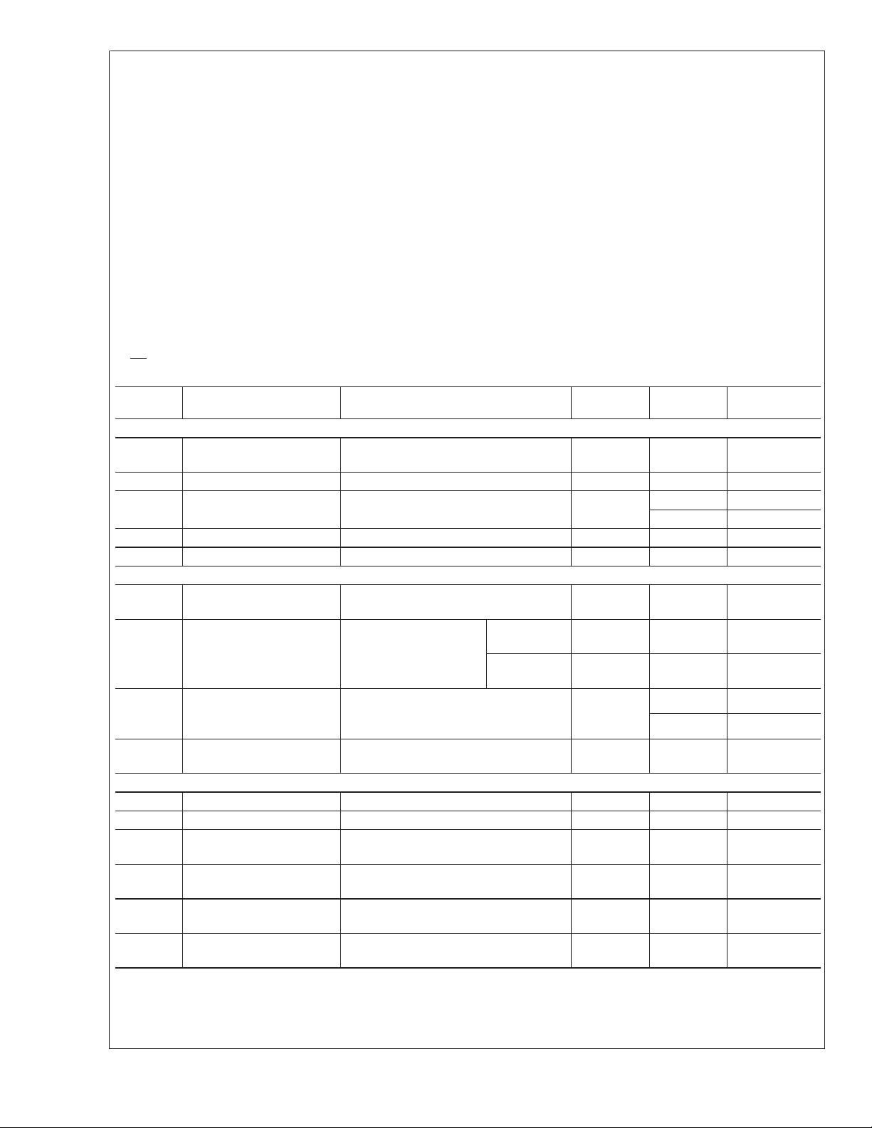
Converter Electrical Characteristics
+
=
=
The following specifications apply for AGND=DGND=DGND I/O=0V, V
PD=+5V, V
=
T
=
T
A
T
J
MIN
REF+ IN
to T
=
+2.0V, V
MAX
REF− IN
: all other limits T
=
AGND, f
A
CLK
=
=
T
25˚C(Notes 7, 8, 9)
J
=
2.5 MHz, C
=
L
V
50 pF/pin. After Auto-Cal. Boldface limits apply for
Symbol Parameter Conditions
Static Converter Characteristics
Resolution with No
Missing Codes
INL Integral Non Linearity At 16 Bits
DNL Differential Non Linearity At 16 Bits
Full-Scale Error
Zero Offset Error +0.1
Reference and Analog Input Characteristics
V
IN
Input Voltage Range
(V
IN+−VIN−
)
(CLK
C
IN
Input Capacitance V
=
1.0V + 0.7Vrms
IN
LOW)
(CLK
HIGH)
Reference Voltage
V
REF
Range [( V
(V
REF−IN
)] (Note 14)
REF+IN
)−
Reference Input
Resistance
Dynamic Converter Characteristics
BW Full Power Bandwidth 8 MHz
SNR Signal-to-Noise Ratio f
SINAD
THD
SFDR
IMD
Signal-to-Noise &
Distortion
Total Harmonic
Distortion
Spurious Free Dynamic
Range
Intermodulation
Distortion
=
500 kHz 80 dB
IN
=
500 kHz 79 dB
f
IN
=
f
500 kHz
IN
=
f
500 kHz
IN
=
f
95 kHz
IN1
=
105 kHz
f
IN2
A
=
V
+5.0V, V
D
Typical
(Note 10)
I/O=3.0V or 5.0V,
D
Limits
(Note 11)
15 Bits(min)
±
3
±
1
±
0.6 3.0
2.0
±
9 LSB(max)
+3 LSB(max)
−2 LSB(min)
±
0.7
1.8
2.2
12 pF
28 pF
1.8 V(min)
2.00
2.2 V(max)
3.5 KΩ
−88 dB
91 dB
−97 dB
Units
%
FS(max)
%
FS(max)
V(min)
V(max)
www.national.com 6
Page 7

ADC16061
DC and Logic Electrical Characteristics
The following specifications apply for AGND=DGND=DGND I/O=0V, V
PD=+5V, V
apply for T
Symbol Parameter Conditions
CLOCK, RD, PD Digital Input Characteristics
V
IN(1)
V
IN(0)
I
IN(1)
I
IN(0)
C
IN
CAL, RESET Digital Input Characteristics
V
IN(1)
V
IN(0)
I
IN(1)
I
IN(0)
C
IN
D00 - D13 Digital Output Characteristics
V
OUT(1)
V
OUT(1)
V
OUT(0)
I
OZ
+I
SC
−I
SC
Power Supply Characteristics
I
A
I
D
I/O
I
D
PSRR
=
+2.0V, V
REF+
=
=
T
A
J
to T
T
MIN
Logical ″1″ Input Voltage V
Logical ″0″ Input Voltage V
Logical ″1″ Input Current V
Logical ″0″ Input Current V
=
REF IN
AGND, f
: all other limits T
MAX
=
2.5 MHz, RS=25Ω,C
CLK
=
=
T
A
+
=
5.25V 2.0 V(min)
+
=
4.75V 0.8 V(max)
=
5.0V 5 µA
IN
=
0V −5 µA
IN
25˚C(Notes 7, 8, 9)
J
VINInput Capacitance 5 pF
+
Logical ″1″ Input Voltage V
Logical ″0″ Input Voltage V
Logical ″1″ Input Current V
Logical ″0″ Input Current V
=
5.25V 3.5 V(min)
+
=
4.75V 1.0 V(max)
=
5.0V 5 µA
IN
=
0V −5 µA
IN
Input Capacitance 5 pF
Logical ″1″ Output
Voltage
Logical ″1″ Output
Voltage
Logical ″0″ Output
Voltage
TRI-STATE Output
Current
Output Short Circuit
Source Current
Output Short Circuit Sink
Current
V
I/O=4.75V, I
D
V
I/O=2.7V, I
D
I/O=5.25V, I
V
D
V
I/O=3.3V, I
D
=
V
OUT
=
V
OUT
=
V
OUT
=
V
OUT
3V or 5V 100 nA
0V −100 nA
0V, V
D
I/O=3V 12 mA
V
D
=
−360 µA 4.5 V(min)
OUT
=
−360 µA 2.5 V(min)
OUT
=
1.6 mA 0.4 V(max)
OUT
=
1.6 mA 0.4 V(max)
OUT
I/O=3V −10 mA
Analog Supply Current PD=VDI/O 70 85 mA(max)
Digital Supply Current PD=VDI/O 7 8 mA(max)
Output Bus Supply
Current
Total Power
Consumption
Power Supply Rejection
Ratio
PD=VDI/O 1 2 mA(max)
PD=V
I/O 390 475 mW(max)
D
PD=DGND
Change in Full Scale as V
goes from
A
4.25V to 5.25V
100 mV
100 kHz riding on V
PP
+
=
=
V
=
50 pF/pin. After Auto-Cal. Boldface limits
L
=
V
D
+5.0V, V
A
Typical
(Note 10)
<
2mW
I/O=3.0V or 5.0V,
D
Limits
(Note 11)
68 dB
A
54 dB
Units
AC Electrical Characteristics
The following specifications apply for AGND=DGND=DGND I/O=0V, V
PD=+5V, V
apply for T
Symbol Parameter Conditions
f
CLK
t
CONV
t
AD
=
+
+2.0V, V
REF
=
=
T
A
J
to T
T
MIN
=
REF IN
AGND, f
: all other limits T
MAX
=
2.5 MHz, RS=25Ω,C
CLK
=
=
T
A
25˚C(Notes 7, 8, 9)
J
Conversion Clock (CLOCK)
Frequency
Conversion Clock Duty Cycle
Conversion Latency 13 Clock Cycles
Aperture Delay 9 ns
+
=
=
V
=
50 pF/pin. After Auto-Cal. Boldface limits
L
=
V
D
+5.0V, V
A
Typical
(Note 10)
I/O=3.0V or 5.0V,
D
Limits
(Note 11)
300 kHz(min)
3 2.5 MHz(max)
45
55
Units
(Limits)
%
(min)
%
(max)
www.national.com7
Page 8

AC Electrical Characteristics (Continued)
+
=
=
The following specifications apply for AGND=DGND=DGND I/O=0V, V
PD=+5V, V
ADC16061
apply for T
=
+
+2.0V, V
REF
=
=
T
A
J
to T
T
MIN
=
REF IN
AGND, f
: all other limits T
MAX
=
2.5 MHz, RS=25Ω,C
CLK
=
=
T
A
J
25˚C(Notes 7, 8, 9)
V
=
50 pF/pin. After Auto-Cal. Boldface limits
L
Symbol Parameter Conditions
t
OD
t
EOCL
t
DATA_VALID
t
AD
t
ON
t
OFF
t
CAL
Note 1: Absolute MaximumRatings indicate limits beyond which damage to the device may occur. Operating Ratings indicate conditions for which thedevice is functional, but do not guarantee specific performance limits. For guaranteed specifications and test conditions, see the Electrical Characteristics. The guaranteed specifications apply only for the test conditions listed. Some performance characteristics may degrade when the device is not operated under the listed test conditions.
Note 2: All voltages are measured with respect to GND=AGND=DGND I/O=0V, unless otherwise specified.
Note 3: When the input voltage at any pin exceeds the power supplies (that is, V
The 50 mA maximum package input current rating limits the number of pins that can safely exceed the power supplies with an input current of 25 mA to two.
Note 4: The absolute maximum junction temperature (T
junction-to-ambient thermal resistance (θ
TQFP, θ
device under normal operation will typically be about 416 mW (390 mW quiescent power + 26 mW due to 1 TTL load on each digital output. The values for maximum
power dissipation listed above will be reached only when the ADC16061 is operated in a severe fault condition (e.g. when input or output pins are driven beyond the
power supply voltages, or the power supply polarity is reversed). Obviously, such conditions should always be avoided.
Note 5: Human body model is 100 pF capacitor discharged through a 1.5kΩ resistor. Machine model is 220 pF discharged through ZERO Ω.
Note 6: See AN450, ″Surface Mounting Methods and Their Effect on Product Reliability″, or the section entitled ″Surface Mount″ found in any post 1986 National
Semiconductor Linear Data Book, for other methods of soldering surface mount devices.
Note 7: The inputs are protected as shown below. Input voltages above V
ever, errors in the A/D conversion can occur if the input goes above V
voltage must be ≤4.85V
is 70˚C/W, so PDMAX = 1,785 mW at 25˚C and 1,142 mW at the maximum operating ambient temperature of 70˚C. Note that the power dissipation of this
JA
Falling edge of CLK to Data
Valid
Falling edge of CLK to falling
edge of EOC
Falling edge of CLOCK to Data
Valid
Aperture Delay 9 ns
RD low to data valid on D00
-D15
RD high to D00 -D15 in
TRI-STATE
Calibration Time 110 ms
), and the ambient temperature (TA), and can be calculated using the formula PDMAX=(TJmax - TA)/θJA. In the 52-pin
JA
to ensure accurate conversions
DC
<
AGND or V
IN
max) for this device is 150˚C. The maximum allowable power dissipation is dictated by TJmax, the
J
or below GND will not damage this device, provided current is limited per Note 3. How-
A
or below GND by more than 100 mV. As an example, if VAis 4.75 VDC, the full-scale input
A
>
VAor VD), the current at that pin should be limited to 25 mA.
IN
V
A
D
Typical
(Note 10)
=
+5.0V, V
I/O=3.0V or 5.0V,
D
Limits
(Note 11)
50 ns
1/(4f
1/(8f
CLK
CLK
)
)
90
130
38
95
23 33 ns(max)
25 33 ns(max)
Units
(Limits)
ns(min)
ns(max)
ns(min)
ns(max)
DS100889-12
DS100889-11
ESD Protection Scheme for Analog Input and Digital
Output pins
ESD Protection Scheme for Digital Input pins
Note 8: To guarantee accuracy, it is required that V
Note 9: With the test condition for V
Note 10: Typical figures are at T
Note 11: Tested limits are guaranteed to Nationsl’s AOQL (Average Outgoing Quality Level) with 50%duty cycle clock.
Note 12: Integral Non Linearity is defined as the deviation of the analog value, expressed in LSBs, from the straight line that passes through positive full-scale and
negative full-scale.
Note 13: Timing specifications are tested at the TTL logic levels, V
to 1.4V.
Note 14: Optimum SNR performance will be obtained by keeping the reference voltage in the 1.8V to 2.2V range. The LM4041CIM3-ADJ (SOT-23 package), or the
LM4041CIZ-ADJ (TO-92 package), bandgap voltage reference is recommended for this application.
=
REF
=
=
T
25˚C, and represent most likely parametric norms.
A
J
www.national.com 8
and VDbe connected together and to the same power supply with separate bypass capacitors at each V+pin.
A
+)−(V
(V
REF
−) given as +2.0V, the 16-bit LSB is 30 µV.
REF
=
0.4V for a falling edge and V
IL
=
2.4V for a rising edge. TRI-STATE output voltage is forced
IH
Page 9

Electrical Characteristics (continued)
ADC16061
FIGURE 1. Transfer Characteristics
FIGURE 2. Errors removed by Auto-Cal cycle
DS100889-13
DS100889-14
www.national.com9
Page 10

Typical Performance Characteristics
INL vs Temperature
ADC16061
INL vs V
and Temperature
REF
DS100889-25
DS100889-35
DNL vs Temperature
DNL vs V
REF
DS100889-26
DS100889-34
SNR vs Temperature
DS100889-27
THD vs Temperaure
DS100889-28
SINAD & ENOB vs Temperature
DS100889-29
IMD
SINAD & ENOB vs Clock Duty
Cycle
Spectral Response
DS100889-30
SFDR vs Temperature
DS100889-31
DS100889-32
www.national.com 10
DS100889-33
Page 11

Specification Definitions
APERTURE JITTER is the variation in aperture delay from
sample to sample. Aperture jitter shows up as input noise.
APERTURE DELAY is the time required after the falling
edge of the clock for the sampling switch to open. In other
words, for the Track/Hold circuit to go from ’track’ mode into
the ’hold’ mode. The Track/Hold circuit affectively stops capturing the input signal and goes into the ’hold’ mode t
the fall of the clock.
OFFSET ERROR is the difference between the ideal LSB
transition to the actual transition point. The LSB transition
should occur when V
+=VIN−.
IN
DIFFERENTIAL NON-LINEARITY (DNL) is the measure of
the maximum deviation from the ideal step size of 1 LSB.
EFFECTIVE NUMBER OF BITS (ENOB, or EFFECTIVE
BITS) is another method of specifying Signal-to-Noise and
Distortion Ratio, or SINAD. ENOB is defined as (SINAD
−1.76) / 6.02.
FULL SCALE ERROR is the difference between the input
voltage [(V
full scale and V
(V
REF−IN
+)−(VIN−)] just causing a transition to positive
IN
− 1.5 LSB, where V
REF
REF
is(V
).
FULL POWER BANDWIDTH is a measure of the frequency
at which the reconstructed output fundamental drops 3 dB
below its low frequency value for a full scale input. The test
is performed with f
of f
. The input frequency at which the output is −3 dB
CLK
equal to 100 kHz plus integral multiples
IN
relative to the low frequency input signal is the full power
bandwidth.
INTERMODULATION DISTORTION (IMD) is the creation of
additional spectral components as a result of two sinusoidal
frequencies being applied to the ADC input at the same time.
AD
REF+IN
after
)−
It is defined as the ratio of the power in the intermodulation
products to the total power in the original frequencies. IMD is
usually expressed in dB.
INTEGRAL NON-LINEARITY (INL) is a measure of the deviation of each individual code from a line drawn from negative full scale (
1
⁄2LSB below the first code transition) through
positive full scale (the last code transition). The deviation of
any given code from this straight line is measured from the
center of that code value.
PIPELINE DELAY (LATENCY) is the number of clock cycles
between initiation of conversion and when that data is presented to the output stage. Data for any given sample is
available the Pipeline Delay plus the Output Delay after that
sample is taken. New data is available at every clock cycle,
but the data lags the conversion by the pipeline delay.
SIGNAL TO NOISE RATIO (SNR) is the ratio, expressed in
dB, of the rms value of the input signal to the rms value of the
sum of all other spectral components below one-half the
sampling frequency, not including harmonics or dc.
SIGNAL TO NOISE PLUS DISTORTION (S/(N+D) or SINAD)) is the ratio, expressed in dB, of the rms value of the
input signal to the rms value of all of the other spectral components below half the clock frequency, including harmonics
but excluding dc.
SPURIOUS FREE DYNAMIC RANGE (SFDR) is the difference, expressed in dB, between the rms values of the input
signal and the peak spurious signal, where a spurious signal
is any signal present in the output spectrum that is not
present at the input.
TOTAL HARMONIC DISTORTION (THD) is the ratio, expressed in dB or dBc, of the rms total of the first six harmonic
components, to the rms value of the input signal.
ADC16061
Timing Diagrams
TIMING DIAGRAM 1. Output Timing
DS100889-15
www.national.com11
Page 12

Timing Diagrams (Continued)
ADC16061
DS100889-16
TIMING DIAGRAM 2. Reset and Calibration Timing
www.national.com 12
Page 13

Functional Description
Operating on a single +5V supply, the ADC16061 uses a
pipelined architecture and has error correction circuitry and a
calibration mode to help ensure maximum performance at all
times.
Balanced analog signals with a peak-to-peak voltage equal
to the input reference voltage, V
the common mode input voltage, V
(15 bits plus sign). Neglecting offsets, positive input signal
voltages (V
+−VIN− ≥ 0) produce positive digital output
IN
data and negative input signal voltages (V
produce negative output data. The input signal can be digitized at any clock rate between 300 Ksps and 2.5 Msps.
Input voltages below the negative full scale value will cause
the output word to take on the negative full scale value of
1000,0000,0000,0000. Input voltage above the positive full
scale value will cause the output word to take on the positive
full scale value of 0111,1111,1111,1111.
The output word rate is the same as the clock frequency.The
analog input voltage is acquired at the falling edge of the
clock and the digital data for that sample is delayed by the
pipeline for 13 clock cycles plus t
put is undefined if the chip is being reset or is in the calibration mode. The output signal may be inhibited by the RD pin
while the converter is in one of these modes.
The RD pin must be low to enable the digital outputs. A logic
low on the power down (PD) pin reduces the converter
power consumption to less than two milliwatts.
, and centered around
REF
, are digitized to 16 bits
CM
+−VIN−<0)
IN
DATA_VALID
. The digital out-
V
REF (MID)
V
CM
is the reference mid-point and is derived from
. This point is brought out only to be by passed. Bypass
this pin with 0.1µF capacitor to ground. Do not load this pin.
It is very important that all grounds associated with the refer-
ence voltage make connection to the analog ground plane at
a single point to minimize the effects of noise currents in the
ground path.
1.3 Signal Inputs
The signal inputs are V
+ and VIN−. The signal input, VIN,
IN
is defined as
=
V
IN
Figure 3
indicates the relationship between the input voltage
and the reference voltages.
+)−(VIN−).
(V
IN
Figure 4
shows the expected in-
put signal range.
ADC16061
Applications Information
1.0 OPERATING CONDITIONS
We recommend that the following conditions be observed for
operation of the ADC16061:
4.75V ≤ V
5.25V ≤ V
3.0V ≤ V
0.3MHz ≤ f
V
CM
V
REF IN
V
REF IN
1.1 The Analog Inputs
TheADC16061 has two analog signal inputs, V
These two pins form a balanced input. There are two reference pins, V
ential input reference.
1.2 Reference Inputs
V
should always be more positive than V
REF+IN
effective reference voltage, V
these two voltages:
The operational voltage range of V
+3.0 Volts. The operational voltage range of V
ground to 1.0V. For best performance, the difference between V
REF+IN
of 1.8V to 2.2V. Reducing the reference voltage below 1.8V
will decrease the signal-to-noise ratio (SNR) of the
ADC16061. Increasing the reference voltage (and, consequently, the input signal swing) above 2.2V will increase
THD.
≤ 5.25V
A
≤ 5.25V
D
I/O ≤ V
D
CLK
=
2.0V (forced)
+=2.0V
−=AGND
REF+IN
=
V
REF
and V
D
≤ 2.5 MHz
and V
REF−IN
(V
REF+IN
REF−IN
+ and VIN−.
IN
. These pins form a differ-
. The
, is the difference between
REF
)−(V
REF−IN
REF+IN
REF−IN
).
is +1.8 Volts to
REF−IN
should remain within the range
DS100889-17
FIGURE 3. Typical Input to Reference Relationship.
DS100889-18
FIGURE 4. Expected Input Signal Range.
The ADC16061 performs best with a balanced input cen-
is
tered around V
V
+orVIN− should be less than the reference voltage and
IN
each signal input pin should be centered on the V
The two V
. The peak-to-peak voltage swing at either
CM
-centered input signals should be exactly 180˚
CM
CM
voltage.
out of phase from each other. As a simple check to ensure
this, be certain that the average voltage at the ADC input
pins is equal to V
. Drive the analog inputs with a source
CM
impedance less than 100 Ohms.
www.national.com13
Page 14

Applications Information (Continued)
The sign bit of the output word will be a logic low when V
is greater than V
ADC16061
bit of the output word will be a logic high.
For single ended operation, one of the analog inputs should
be connected to V
duced by about 12dB with a single ended input as compared
with differential inputs.
An input voltage of V
preted as mid-scale and will thus be converted to
0000,0000,0000,0000, plus any offset error.
The V
+ and the VIN− inputs of the ADC16061 consist of an
IN
analog switch followed by a switched-capacitor amplifier.
The capacitance seen at the analog input pins changes with
the clock level, appearing as 12 pF when the clock is low,
and 28 pF when the clock is high. It is recommended that the
ADC16061 be driven with a low impedance source of 100
Ohms or less.
Since a dynamic capacitance is more difficult to drive than is
a fixed capacitance, choose driving amplifiers carefully. The
CLC440, LM6152, LM6154, LM6172, LM6181 and LM6182
are good amplifiers for driving the ADC16061.
Asimple application circuit is shown in
Here we use two LM6172 dual amplifiers to provide a balanced input to the ADC16061. Note that better noise performance is achieved when V
well-bypassed resistive divider. The resulting offset and offset drift is minimal.
1.4 V
The V
of the V
The V
Analog Inputs
CM
input of the ADC16061 is internally biased to 40
CM
supply with on-chip resistors, as shown in
A
pin must be bypassed to prevent any power supply
CM
noise from modulating this voltage. Modulation of the V
potential will result in the introduction of noise into the input
signal. The advantage of simply bypassing V
driving it) is the circuit simplicity.On the other hand, if the V
supply can vary for any reason, VCMwill also vary at a rate
and amplitude related to the RC filter created by the bypass
capacitor and the internal divider resistors. However, performance of this approach will be adequate for many
applications.
FIGURE 5. VCMinput to the ADC16061 VCMis set to
40%of V
improved when V
By forcing V
lems mentioned above. One such approach is to buffer the
2.0 Volt reference voltage to drive the V
a constant potential as shown in
reference voltage is different from the desired V
sired V
voltage may be derived from the reference or from
CM
another stable source.
− . When VIN+ is less than VIN−, the sign
IN
. However, SNR and SINAD are re-
CM
=
+)−(VIN−)=0 will be inter-
(V
IN
IN
Figure 6
REF+IN
with on-chip resistors. Performance is
A
is driven with a stable, low
CM
voltage is forced with a
DS100889-21
impedance source
to a fixed potential, you can avoid the prob-
CM
input, holding it at
CM
Figure 6
and
Figure 8
and
CM
CM
IN
Figure 7
%
Figure 5
CM
(without
.Ifthe
, that de-
Note that the buffer used for this purpose should be a slow,
low noise amplifier. The LMC660, LMC662, LMC272 and
+
LMC7101 are good choices for driving the V
CM
pin of the
ADC16061.
If it is desired to use a multiplexer at the analog input, that
multiplexer should be switched at the rising edge of the clock
signal.
2.0 DIGITAL INPUTS
Digital Inputs consist of CLOCK, RESET, CAL, RD and PD.
All digital input pins should remain stable from the fall of the
clock until 30ns after the fall of the clock to minimize digital
noise corruption of the input signal on the die.
2.1 The CLOCK signal drives an internal phase delay loop to
create timing for theADC. Drive the clock input with a stable,
low phase jitter clock signal in the range of 300 kHz to 2.5
MHz. The trace carrying the clock signal should be as short
as possible. This trace should not cross any other signal line,
analog or digital, not even at 90˚.
The CLOCK signal also drives the internal state machine. If
the clock is interrupted, the data within the pipeline could become corrupted.
A 100 Ohm damping resistor should be placed in series with
.
the CLOCK pin to prevent signal undershoot at that input.
2.2 The RESET input is level sensitive and must be pulsed
high for at least two clock cycles to reset the ADC after
power-up and before calibration (See Timing Diagram 2).
2.3 The CAL input is level sensitive and must be pulsed high
for at least two clock cycles to begin ADC calibration (See
Timing Diagram 2). Reset the ADC16061 before calibrating.
Re-calibrate after the temperature has changed by more
.
than 50˚C since the last calibration was performed and after
return from power down.
During calibration, use the same clock frequency that will be
used for conversions to avoid excessive offset errors.
A
Calibration takes 272,800 clock cycles. Irrelevant data may
appear at the data outputs during RESET or CAL and for 13
clock cycles thereafter.Calibration should not be started until
the reference outputs have settled (100ms with 1µF capacitors on these outputs) after power up or coming out of the
power down mode.
2.4 RD pin is used to READ the conversion data. When the
RD pin is low, the output buffers go into the active state.
When the RD input is high, the output buffers are in the high
impedance state.
2.5 The PD pin, when low, holds the ADC16061 in a
power-down mode where power consumption is typically
less than 2mW to conserve power when the converter is not
being used. Power consumption during shut-down is not affected by the clock frequency, or by whether there is a clock
signal present. The data in the pipeline is corrupted while in
the power down mode. The ADC16061 should be reset and
calibrated upon returning to normal operation after a power
down.
3.0 OUTPUTS
The ADC16061 has four analog outputs: V
V
REF−OUT,VREF (MID)
and VCM. There are 17 digital out-
REF+OUT
,
puts: EOC (End of Conversion) and 16 Data Output pins.
3.1 The reference output voltages are made available only
for the purpose of bypassing with capacitors. These pins
should not be loaded with more than 10 µADC. These output
voltages are described as
V
REF+OUT
=
+1⁄2V
V
CM
REF
www.national.com 14
Page 15

Applications Information (Continued)
V
REF−OUT
where V
V
REF (MID)
REF
=
To avoid signal clipping and distortion, V
exceed 3.3V, V
V
should be held in the range of 1.8V to 2.2V.
CM
REF−OUT
3.2 The EOC output goes low to indicate the presence of
valid data at the output data lines. Valid data is present the
entire time that this signal is low,except during reset. Corrupt
or irrelevant data may appear at the data outputs when the
RESET pin or the CAL pin is high.
3.3 The Data Outputs are TTL/CMOS compatible. The output data format is two’s complement. Valid data is present at
these outputs while the EOC pin is low. While the t
and the t
DATA_VALID
timing, a simple way to capture a valid output is to latch the
data on the rising edge of the CLOCK (pin 10).
Also helpful in minimizing noise due to output switching is to
minimize the load currents at the digital outputs. This can be
done by connecting buffers between the ADC outputs and
any other circuitry. Only one input should be connected to
each output pin. Additionally, inserting series resistors of 47
or 56 Ohms at the digital outputs, close to the ADC pins, will
isolate the outputs from other circuitry and limit output currents. (See
Figure 6
=
−1⁄2V
V
=
(V
CM
(V
REF+IN
REF+OUT+VREF−OUT
)−(V
REF
+ IN)
REF
REF+OUT
)/2.
should not
should not be below 750 mV and
time
EOCL
time provide information about output
).
4.0 POWER SUPPLY CONSIDERATIONS
Each power supply pin should be bypassed with a parallel
combination of a 10 µF capacitor and a 0.1 µF ceramic chip
capacitor.The chip capacitors should be within
1
⁄2centimeter
of the power pins. Leadless chip capacitors are preferred because they provide low lead inductance.
While a single 5V source is used for the analog and digital
supplies of the ADC16061, these supply pins should be well
isolated from each other to prevent any digital noise from being coupled to the analog power pins. Supply isolation with
ferrite beads is shown in
Figure 6
and
Figure 8
.
As is the case with all high-speed converters, the ADC16061
is sensitive to power supply noise. Accordingly, the noise on
the analog supply pin should be kept below 15 mV
P-P
.
No pin should ever have a voltage on it that is in excess of
the supply voltages, not even during power up or power
down.
The V
I/O provides power for the output drivers and may be
D
operated from a supply in the range of 2.7V to the V
supply
D
(nominal 5V). This can simplify interfacing to 3.0 Volt devices
and systems. Powering V
I/O from 3 Volts will also reduce
D
power consumption and noise generation due to output
switching. DO NOT operate the V
than V
or VA.
D
I/O at a voltage higher
D
ADC16061
FIGURE 6. Simple application circuit with single-ended to differential buffer.
DS100889-19
www.national.com15
Page 16

Applications Information (Continued)
ADC16061
FIGURE 7. Differential drive circuit of
Figure 6
DS100889-20
. All 5k resistors are 0.1%. Tolerance of the other resistors is not
critical.
FIGURE 8. Driving the signal inputs with a transformer.
www.national.com 16
DS100889-22
Page 17

Applications Information (Continued)
5.0 LAYOUT AND GROUNDING
Proper grounding and proper routing of all signals are essential to ensure accurate conversion. Separate analog and
digital ground planes that are connected beneath the
ADC16061 are required to achieve specified performance.
The analog and digital grounds may be in the same layer,but
should be separated from each other and should never overlap each other. Separation should be at least
possible.
The ground return for the digital supply (DGND I/O ) carries
the ground current for the output drivers. This output current
can exhibit high transients that could add noise to the conversion process. To prevent this from happening, the DGND
I/O pin should NOT be connected in close proximity to any of
the ADC16061’s other ground pins.
Capacitive coupling between the typically noisy digital
ground plane and the sensitive analog circuitry can lead to
poor performance that may seem impossible to isolate and
remedy. The solution is to keep the analog circuitry separated from the digital circuitry and from the digital ground
plane.
Digital circuits create substantial supply and ground current
transients. The logic noise thus generated could have significant impact upon system noise performance. The best logic
family to use in systems with A/D converters is one which
employs non-saturating transistor designs, or has low noise
characteristics, such as the 74LS, 74HC(T) and 74AC(T)Q
families. The worst noise generators are logic families that
draw the largest supply current transients during clock or signal edges, like the 74F and the 74AC(T) families.
Since digital switching transients are composed largely of
high frequency components, total ground plane copper
weight will have little effect upon the logic-generated noise.
This is because of the skin effect. Total surface area is more
important than is total ground plane volume.
An effective way to control ground noise is by connecting the
analog and digital ground planes together beneath the ADC
with a copper trace that is very narrow compared with the
1
⁄8inch, where
rest of the ground plane. A typical width is 3/16 inch (4 to 5
mm).This narrowing beneath the converter provides a fairly
high impedance to the high frequency components of the
digital switching currents, directing them away from the analog pins. The relatively lower frequency analog ground currents see a relatively low impedance across this narrow
ground connection.
Generally,analog and digitallines should cross each other at
90 degrees to avoid getting digital noise into the analog path.
To maximize accuracy in high speed, high resolution systems, however, avoid crossing analog and digital lines altogether. It is important to keep any clock lines isolated from
ALL other lines, including other digital lines. Even the generally accepted 90 degree crossing should be avoided as even
a little coupling can cause problems at high frequencies.
This is because other lines can introduce phase noise (jitter)
into the clock line, which can lead to degradation of SNR.
Best performance at high frequencies and at high resolution
is obtained with a straight signal path. That is, the signal path
through all components should form a straight line wherever
possible.
Be especially careful with the layout of inductors. Mutual inductance can change the characteristics of the circuit in
which they are used. Inductors should not be placed side by
side, not even with just a small part of their bodies beside
each other.
The analog input should be isolated from noisy signal traces
to avoid coupling of spurious signals into the input. Any external component (e.g., a filter capacitor) connected between the converter’s input and ground should be connected
to a very clean point in the analog ground plane.
Figure 9
cuitry (input amplifiers, filters, reference components, etc.)
should be placed on or over the analog ground plane. All
digital circuitry and I/O lines should be placed over the digital
ground plane.
All ground connections should have a low inductance path to
ground.
gives an example of a suitable layout.All analog cir-
ADC16061
www.national.com17
Page 18

Applications Information (Continued)
ADC16061
FIGURE 9. Example at a suitable layout.
6.0 DYNAMIC PERFORMANCE
To achieve the best dynamic performance with the
ADC16061, the clock source driving the CLK input must be
free of jitter. For best ac performance, isolate the ADC clock
from any digital circuitry with buffers, as with the clock tree
shown in
Figure 10
.
As mentioned in section 5.0, it is good practice to keep the
ADC clock line as short as possible and to keep it well away
from any other signals. Other signals can introduce phase
noise (jitter) into the clock signal, which can lead to increased distortion. Even lines with 90˚ crossings have capacitive coupling, so try to avoid even these 90˚ crossings of
the clock line.
DS100889-24
FIGURE 10. Isolating the ADC clock from other
circuitry with a clock tree.
7.0 COMMON APPLICATION PITFALLS
Driving the inputs (analog or digital) beyond the power
supply rails. For proper operation, all inputs should not go
more than 100 mV beyond the supply rails (more than 100
DS100889-23
mV below the ground pins or 100 mV above the supply pins).
Exceeding these limits on even a transient basis may cause
faulty or erratic operation. It is not uncommon for high speed
digital circuits (e.g., 74F and 74AC devices) to exhibit undershoot that goes more than a volt below ground. A resistor of
about 50 to 100Ω in series with the offending digital input will
eliminate the problem.
Do not allow input voltages to exceed the supply voltage during power up.
Be careful not to overdrive the inputs of the ADC16061 with
a device that is powered from supplies outside the range of
theADC16061 supply. Such practice may lead to conversion
inaccuracies and even to device damage.
Attempting to drive a high capacitance digital data bus.
The more capacitance the output drivers must charge for
each conversion, the more instantaneous digital current
flows through V
I/O and DGND I/O. These large charging
D
current spikes can couple into the analog circuitry of the
ADC16061, degrading dynamic performance. Adequate bypassing and maintaining separate analog and digital ground
planes will reduce this problem. The digital data outputs
should be buffered (with 74ACQ541, for example). Dynamic
performance can also be improved by adding series resistors at each digital output, close to the ADC16061, which reduces the energy coupled back into the converter output
pins by limiting the output current. A reasonable value for
these resistors is 47Ω.
Using an inadequate amplifier to drive the analog input.
As explained in Section 1.3, the capacitance seen at the input alternates between 12 pF and 28 pF,depending upon the
phase of the clock. This dynamic load is more difficult to
drive than is a fixed capacitance.
If the amplifier exhibits overshoot, ringing, or any evidence of
instability, even at a very low level, it will degrade perfor-
www.national.com 18
Page 19

Applications Information (Continued)
mance. Amplifiers that have been used successfully to drive
the analog inputs of the ADC16061 include the CLC427,
CLC440, LM6152, LM6154, LM6181 and the LM6182. A
small series reistor at each amplifier output and a capacitor
across the analog inputs (as shown in
prove performance.
Operating with the reference pins outside of the specified range. As mentioned in section 1.2, V
the range of
1.8V ≤ V
REF
≤ 2.2V
Figure 7
REF
) will often im-
should be in
with V
≤ 1.0V. Operating outside of these limits could
REF−IN
lead to excessive distortion or noise.
Using a clock source with excessive jitter, using an excessively long clock signal trace, or having other signals coupled to the clock signal trace. This will cause the
sampling interval to vary, causing excessive output noise
and a reduction in SNR performance.
Connecting pins marked ″NC″ to any potential. Some of
these pins are used for factory testing. They should all be left
floating. Connecting them to ground, power supply, or some
other voltage could result in a non-functional device.
ADC16061
www.national.com19
Page 20

Physical Dimensions inches (millimeters) unless otherwise noted
52-Lead Thin Quad Flat Pack
Ordering Number ADC16061CCVT
NS Package Number VEG52A
ADC16061 Self-Calibrating 16-Bit, 2.5 MSPS, 390 mW A/D Converter
LIFE SUPPORT POLICY
NATIONAL’S PRODUCTS ARE NOT AUTHORIZED FOR USE AS CRITICAL COMPONENTS IN LIFE SUPPORT
DEVICES OR SYSTEMS WITHOUT THE EXPRESS WRITTEN APPROVAL OF THE PRESIDENT AND GENERAL
COUNSEL OF NATIONAL SEMICONDUCTOR CORPORATION. As used herein:
1. Life support devices or systems are devices or
systems which, (a) are intended for surgical implant
into the body, or (b) support or sustain life, and
whose failure to perform when properly used in
accordance with instructions for use provided in the
labeling, can be reasonably expected to result in a
significant injury to the user.
National Semiconductor
Corporation
Americas
Tel: 1-800-272-9959
Fax: 1-800-737-7018
Email: support@nsc.com
www.national.com
National Semiconductor
Europe
Fax: +49 (0) 1 80-530 85 86
Email: europe.support@nsc.com
Deutsch Tel: +49 (0) 1 80-530 85 85
English Tel: +49 (0) 1 80-532 78 32
Français Tel: +49 (0) 1 80-532 93 58
Italiano Tel: +49 (0) 1 80-534 16 80
2. A critical component is any component of a life
support device or system whose failure to perform
can be reasonably expected to cause the failure of
the life support device or system, or to affect its
safety or effectiveness.
National Semiconductor
Asia Pacific Customer
Response Group
Tel: 65-2544466
Fax: 65-2504466
Email: sea.support@nsc.com
National Semiconductor
Japan Ltd.
Tel: 81-3-5639-7560
Fax: 81-3-5639-7507
National does not assume any responsibility for use of any circuitry described, no circuit patent licenses are implied and National reserves the right at any time without notice to change said circuitry and specifications.
 Loading...