

Page 1
ADVANCE INFORMATION
January 25, 2008
ADC12EU050
Ultra-Low Power, Octal, 12-bit, 40-50 MSPS Analog-toDigital Converter
General Description
NOTE: This is Advance Information for a product currently in development. ALL specifications are design targets and are subject to change.
The ADC12EU050 is a 12-bit, ultra-low power, octal A/D converter for use in high performance analog to digital applications. The ADC12EU050 uses an innovative continuous time
sigma delta architecture offering ultra low power consumption
and an alias free sample bandwidth up to 25MHz. The input
stage of each channel features a proprietary system to ensure
instantaneous recovery from overdrive. Instant overload recovery (IOR) with no memory effect guarantees the elimination of phase errors resulting from out of range input signals.
The ADC12EU050 reduces interconnection complexity by using programmable serialized outputs which offer the industry
standard LVDS and SLVS modes. Power consumption of only
44mW per channel(@ 50MSPS) gives a total chip power consumption of 350mW. The ADC12EU050 can operate entirely
from a 1.2V supply, although a separate output driver supply
of up to 1.8V can be used. The device operates from -40 to
+85 °C and is supplied in a 10 x 10 mm2, 68 pin package.
Features
■
CT∑ΔADC architecture with 40-50MSPS throughput
■
Anti-alias filter free Nyquist sample range
■
Unique Instant Overload Recovery (IOR)
■
Wide 2.10 VPP input range
■
1.2V supply voltage
■
Integrated precision LC PLL
■
Serial control via SPI compatible interface
Key Specifications
■
Resolution 12 Bits
■
Conversion Rate 40 to 50 MSPS
■
SNR 70 dBFS (typ) @ (fIN = 3.5MHz)
■
THD –70 dB (typ) @ (fIN = 3.5MHz)
■
Power Consumption 44 mW/ch (typ) @ 50MSPS
■
40 mW/ch (typ) @ 40MSPS
■
Total Active Power
Consumption
350 mW (typ) @ 50MSPS
(Equalizer off)
■
Inter-Channel Isolation >110 dB @ (fIN = 3.5MHz)
■
Operating Temp. Range -40 to +85 °C
Applications
■
Battery powered portable systems
■
Medical imaging, ultrasound
■
Industrial ultrasound, such as non-destructive testing
■
Communications
© 2008 National Semiconductor Corporation 300511 www.national.com
ADC12EU050 Ultra-Low Power, Octal, 12-bit, 40-50 MSPS Analog-to-Digital Converter
Page 2
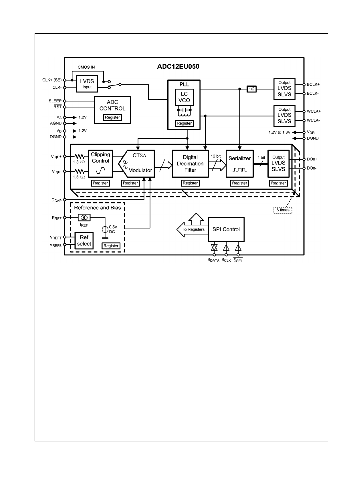
Block Diagram
30051102
www.national.com 2
ADC12EU050
Page 3
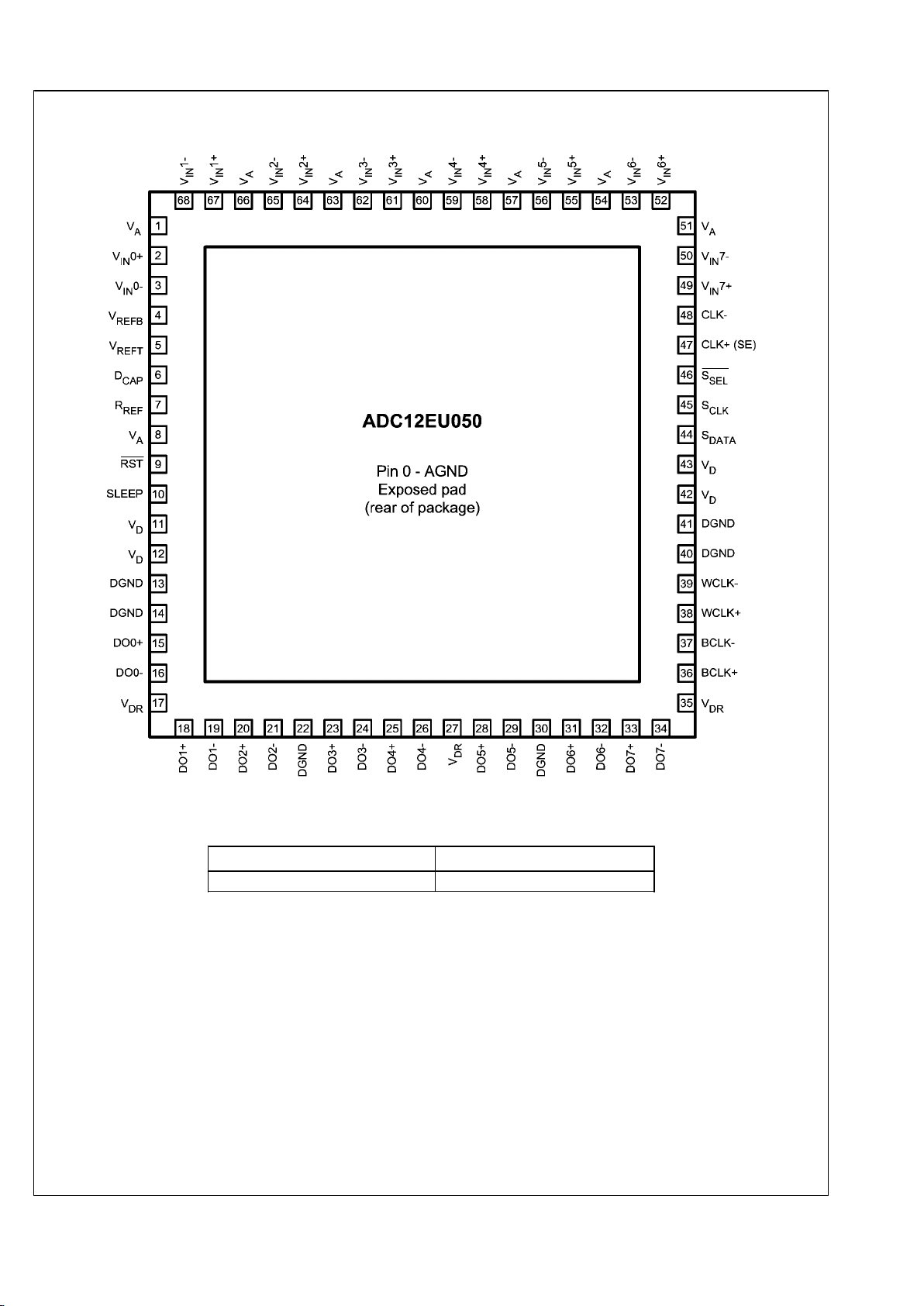
Connection Diagram
30051101
Ordering Information
Industrial (−40°C ≤ TA ≤ +85°C)
Package
ADC12EU050CILQ 68 Pin LLP
Note:
The ADC12EU050 evaluation systems comprise a fully populated &
tested device board (DUT), a data capture card with USB 2.0 interface, a SPI control daughter board, Merlin® time and frequency
domain measurement software and 2 USB connection cables. The
ADC12EU050 evaluation kit is not compatible with National
Semiconductor’s Wavevision capture board and software.
3 www.national.com
ADC12EU050
Page 4

Pin Descriptions
Pin No. Name Type Function and Connection
ANALOG I/O
2
3
67
68
64
65
61
62
58
59
55
56
52
53
49
50
VIN0+
VIN0-
VIN1+
VIN1-
VIN2+
VIN2-
VIN3+
VIN3-
VIN4+
VIN4-
VIN5+
VIN5-
VIN6+
VIN6-
VIN7+
VIN7-
Input
Differential analog inputs to the ADC, for channels 0 to 7. The
negative input pin may be connected to AGND or the inputs may
be transformer coupled for single ended operation. A differential
input is recommended for best performance.
4
V
REFB
Optional negative reference voltage to improve multi-channel ADC
matching. If no reference is supplied, this pin must be connected
to AGND.
5
V
REFT
Optional positive reference voltage to improve multi-channel ADC
matching. If using the internal reference, this pin should be left
unconnected. If using an external reference voltage, this pin should
be connected to the positive reference voltage, which must lie in
the range specified in the Electrical Characteristics table.
6
D
CAP
Input
This pin provides the capacitance for the low pass filter in the
modulator’s DAC. It must be connected to AGND through a
minimum 100nF capacitor. It is possible to decrease the noise
close to the carrier by increasing this capacitor, up to a maximum
of 10μF.
7
R
REF
Input/Output
External bias reference resistor. This pin must always be
connected to AGND through a resistor, whether the internal or an
external reference voltage is used. The resistor value must be
10kΩ ±1%.
DIGITAL I/O
9 RST Input
This pin is an active low reset for the entire ADC, both analog and
digital components. The pin must be held low for 500ns then
returned to high in order to ensure that the chip is reset correctly.
10 SLEEP Input
Sleep mode. Toggling this pin to high will cause the ADC to enter
the low power sleep mode. When the pin is returned to low, the
chip will, after the specified time to exit sleep mode, return to normal
operation.
www.national.com 4
ADC12EU050
Page 5

Pin No. Name Type Function and Connection
15
16
18
19
20
21
23
24
25
26
28
29
31
32
33
34
DO0+
DO0-
DO1+
DO1-
DO2+
DO2-
DO3+
DO3-
DO4+
DO4-
DO5+
DO5-
DO6+
DO6-
DO7+
DO7-
Output
Differential Serial Outputs for channels 0 to 7. Each pair of outputs
provides the serial output for the specific channel. The default
output is LVDS format, but programming the appropriate control
registers, the output format can be changed to SLVS.
By programming TX_term (bit 4) in the LVDS Control register, it is
possible to internally terminate these outputs with 100 ohm
resistors.
36
37
BCLK+
BCLK-
Output
Bit clock. Differential output clock to be used for sampling the serial
outputs. Information on timing can be seen in the Electrical
Specifications section of the datasheet.
By programming TX_term (bit 4) in the LVDS Control register, it is
possible to internally terminate these outputs with 100 ohm
resistors.
38
39
WCLK+
WCLK-
Output
Word Clock. Differential output frame clock. Information on timing
can be seen in the Electrical Specifications section of the
datasheet.
By programming TX_term (bit 4) in the LVDS Control register, it is
possible to internally terminate these outputs with 100 ohm
resistors.
44
S
DATA
Input/Output
SPI data input and output. This pin is used to send and receive SPI
address and data information. The direction of the pin is controlled
internally by the ADC based on the SPI protocol.
45
S
CLK
Input
SPI clock. In order to use the SPI interface, a clock must be
provided on this pin. The maximum frequency of operation for the
serial interface is 1MHz.
46
S
SEL
Input
SPI chip select. This active low pin is used to enable the serial
interface.
47
48
CLK+ (SE)
CLK-
Input
Differential Input Clock. The input clock must lie in the range of
40MHz to 50MHz. It is used by the PLL to generate the internal
sampling clocks. A single ended clock can also be used, and
should be connected to pin 47.
POWER SUPPLY
1, 8, 51, 54,
57, 60, 63, 66
V
A
Power
Analog Power Supply. All pins should be connected to the same
1.2V supply, with voltage limits as in the Electrical Specification.
0 AGND Ground Analog Ground Return.
11, 12, 42, 43
V
D
Power
Digital Power Supply. Connect to 1.2V, with voltage limits as in the
Electrical Specification.
13, 14, 22,
30, 40, 41
DGND Ground Digital and Output Driver Ground Return.
17, 27, 35
V
DR
Power
Output Driver Power Supply. Can be connected to 1.2V – 1.8V,
depending on application requirements. Voltage limits are
described in more detail in the Electrical Specification.
5 www.national.com
ADC12EU050
Page 6

Physical Dimensions inches (millimeters) unless otherwise noted
TOP View...............................SIDE View...............................BOTTOM View
68-Lead LLP Package 10x10x1.0mm, 0.5mm Pitch
Ordering Numbers ADC12EU050CILQ
NS Package Number LQA68A
www.national.com 6
ADC12EU050
Page 7

Notes
7 www.national.com
ADC12EU050
Page 8

Notes
ADC12EU050 Ultra-Low Power, Octal, 12-bit, 40-50 MSPS Analog-to-Digital Converter
For more National Semiconductor product information and proven design tools, visit the following Web sites at:
Products Design Support
Amplifiers www.national.com/amplifiers WEBENCH www.national.com/webench
Audio www.national.com/audio Analog University www.national.com/AU
Clock Conditioners www.national.com/timing App Notes www.national.com/appnotes
Data Converters www.national.com/adc Distributors www.national.com/contacts
Displays www.national.com/displays Green Compliance www.national.com/quality/green
Ethernet www.national.com/ethernet Packaging www.national.com/packaging
Interface www.national.com/interface Quality and Reliability www.national.com/quality
LVDS www.national.com/lvds Reference Designs www.national.com/refdesigns
Power Management www.national.com/power Feedback www.national.com/feedback
Switching Regulators www.national.com/switchers
LDOs www.national.com/ldo
LED Lighting www.national.com/led
PowerWise www.national.com/powerwise
Serial Digital Interface (SDI) www.national.com/sdi
Temperature Sensors www.national.com/tempsensors
Wireless (PLL/VCO) www.national.com/wireless
THE CONTENTS OF THIS DOCUMENT ARE PROVIDED IN CONNECTION WITH NATIONAL SEMICONDUCTOR CORPORATION
(“NATIONAL”) PRODUCTS. NATIONAL MAKES NO REPRESENTATIONS OR WARRANTIES WITH RESPECT TO THE ACCURACY
OR COMPLETENESS OF THE CONTENTS OF THIS PUBLICATION AND RESERVES THE RIGHT TO MAKE CHANGES TO
SPECIFICATIONS AND PRODUCT DESCRIPTIONS AT ANY TIME WITHOUT NOTICE. NO LICENSE, WHETHER EXPRESS,
IMPLIED, ARISING BY ESTOPPEL OR OTHERWISE, TO ANY INTELLECTUAL PROPERTY RIGHTS IS GRANTED BY THIS
DOCUMENT.
TESTING AND OTHER QUALITY CONTROLS ARE USED TO THE EXTENT NATIONAL DEEMS NECESSARY TO SUPPORT
NATIONAL’S PRODUCT WARRANTY. EXCEPT WHERE MANDATED BY GOVERNMENT REQUIREMENTS, TESTING OF ALL
PARAMETERS OF EACH PRODUCT IS NOT NECESSARILY PERFORMED. NATIONAL ASSUMES NO LIABILITY FOR
APPLICATIONS ASSISTANCE OR BUYER PRODUCT DESIGN. BUYERS ARE RESPONSIBLE FOR THEIR PRODUCTS AND
APPLICATIONS USING NATIONAL COMPONENTS. PRIOR TO USING OR DISTRIBUTING ANY PRODUCTS THAT INCLUDE
NATIONAL COMPONENTS, BUYERS SHOULD PROVIDE ADEQUATE DESIGN, TESTING AND OPERATING SAFEGUARDS.
EXCEPT AS PROVIDED IN NATIONAL’S TERMS AND CONDITIONS OF SALE FOR SUCH PRODUCTS, NATIONAL ASSUMES NO
LIABILITY WHATSOEVER, AND NATIONAL DISCLAIMS ANY EXPRESS OR IMPLIED WARRANTY RELATING TO THE SALE
AND/OR USE OF NATIONAL PRODUCTS INCLUDING LIABILITY OR WARRANTIES RELATING TO FITNESS FOR A PARTICULAR
PURPOSE, MERCHANTABILITY, OR INFRINGEMENT OF ANY PATENT, COPYRIGHT OR OTHER INTELLECTUAL PROPERTY
RIGHT.
LIFE SUPPORT POLICY
NATIONAL’S PRODUCTS ARE NOT AUTHORIZED FOR USE AS CRITICAL COMPONENTS IN LIFE SUPPORT DEVICES OR
SYSTEMS WITHOUT THE EXPRESS PRIOR WRITTEN APPROVAL OF THE CHIEF EXECUTIVE OFFICER AND GENERAL
COUNSEL OF NATIONAL SEMICONDUCTOR CORPORATION. As used herein:
Life support devices or systems are devices which (a) are intended for surgical implant into the body, or (b) support or sustain life and
whose failure to perform when properly used in accordance with instructions for use provided in the labeling can be reasonably expected
to result in a significant injury to the user. A critical component is any component in a life support device or system whose failure to perform
can be reasonably expected to cause the failure of the life support device or system or to affect its safety or effectiveness.
National Semiconductor and the National Semiconductor logo are registered trademarks of National Semiconductor Corporation. All other
brand or product names may be trademarks or registered trademarks of their respective holders.
Copyright© 2008 National Semiconductor Corporation
For the most current product information visit us at www.national.com
National Semiconductor
Americas Technical
Support Center
Email:
new.feedback@nsc.com
Tel: 1-800-272-9959
National Semiconductor Europe
Technical Support Center
Email: europe.support@nsc.com
German Tel: +49 (0) 180 5010 771
English Tel: +44 (0) 870 850 4288
National Semiconductor Asia
Pacific Technical Support Center
Email: ap.support@nsc.com
National Semiconductor Japan
Technical Support Center
Email: jpn.feedback@nsc.com
www.national.com
 Loading...