

Page 1
February 2007
ADC12C170
12-Bit, 170 MSPS, 1.1 GHz Bandwidth A/D Converter with
CMOS outputs
General Description
The ADC12C170 is a high-performance CMOS analog-todigital converter capable of converting analog input signals
into 12-Bit digital words at rates up to 170 Mega Samples Per
Second (MSPS). This converter uses a differential, pipelined
architecture with digital error correction and an on-chip sample-and-hold circuit to minimize power consumption and the
external component count, while providing excellent dynamic
performance. A unique sample-and-hold stage yields a fullpower bandwidth of 1.1 GHz. The ADC12C170 operates from
dual +3.3V and +1.8V power supplies and consumes 715 mW
of power at 170 MSPS.
The separate +1.8V supply for the digital output interface allows lower power operation with reduced noise. A powerdown feature reduces the power consumption to 5 mW while
still allowing fast wake-up time to full operation. In addition
there is a sleep feature which consumes 50 mW of power and
has a faster wake-up time.
The differential inputs provide a full scale differential input
swing equal to 2 times the reference voltage. A stable 1.0V
internal voltage reference is provided, or the ADC12C170 can
be operated with an external reference.
Clock mode (differential versus single-ended) and output data
format (offset binary versus 2's complement) are pin-selectable. A duty cycle stabilizer maintains performance over
a wide range of input clock duty cycles.
The ADC12C170 is pin compatible with the ADC14155.
It is available in a 48-lead LLP package and operates over the
industrial temperature range of −40°C to +85°C.
Features
■
1.1 GHz Full Power Bandwidth
■
Internal sample-and-hold circuit
■
Low power consumption
■
Internal precision 1.0V reference
■
Single-ended or Differential clock modes
■
Clock Duty Cycle Stabilizer
■
Dual +3.3V and +1.8V supply operation (+/- 10%)
■
Power-down and Sleep modes
■
Offset binary or 2's complement output data format
■
Pin-compatible with: ADC14155
■
48-pin LLP package, (7x7x0.8mm, 0.5mm pin-pitch)
Key Specifications
■
Resolution 12 Bits
■
Conversion Rate 170 MSPS
■
SNR (fIN = 70 MHz) 67.2 dBFS (typ)
■
SFDR (fIN = 70 MHz) 85.4 dBFS (typ)
■
ENOB (fIN = 70 MHz) 10.8 bits (typ)
■
Full Power Bandwidth 1.1 GHz (typ)
■
Power Consumption 715 mW (typ)
Applications
■
High IF Sampling Receivers
■
Wireless Base Station Receivers
■
Power Amplifier Linearization
■
Multi-carrier, Multi-mode Receivers
■
Test and Measurement Equipment
■
Communications Instrumentation
■
Radar Systems
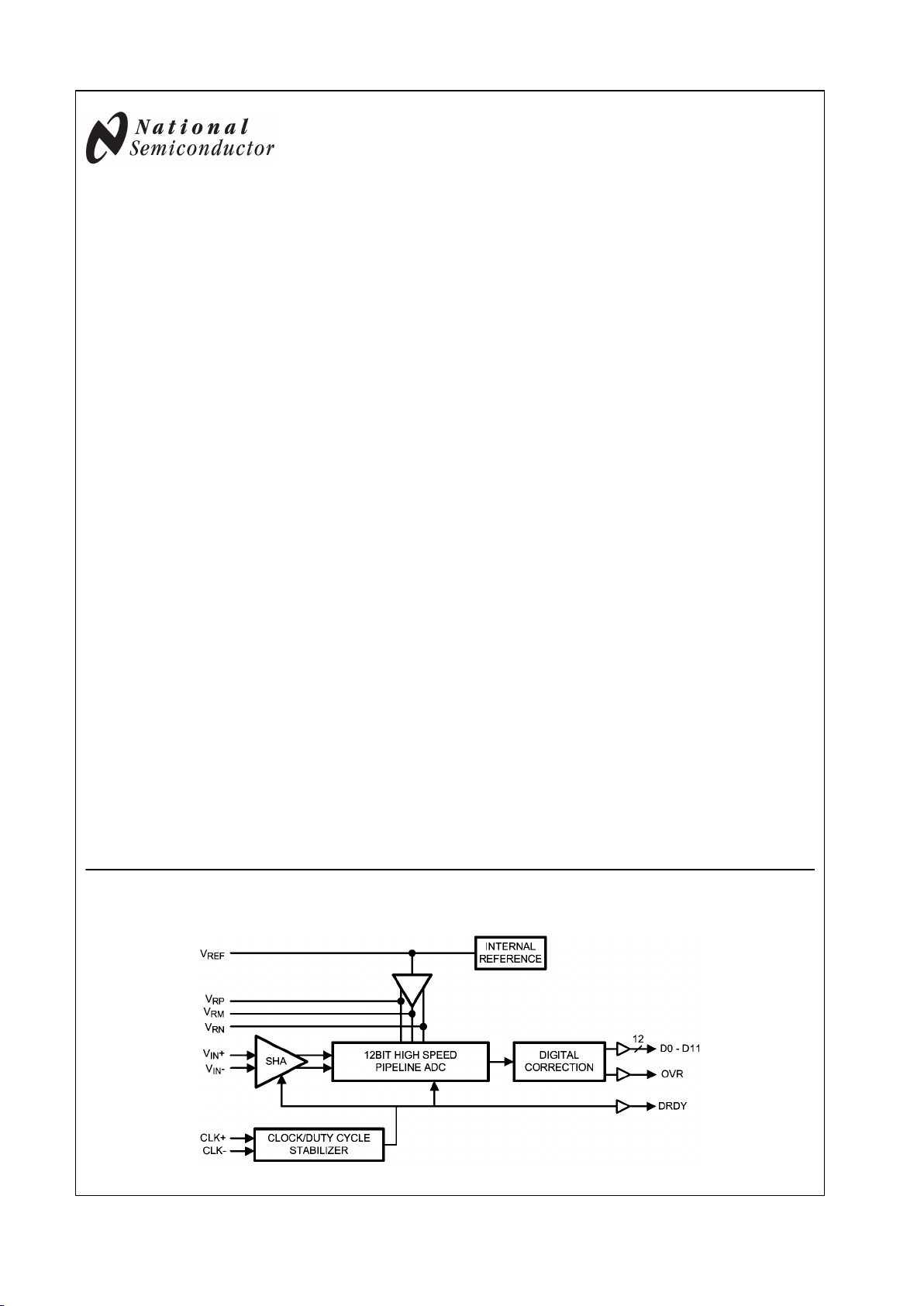
Block Diagram
20209202
© 2007 National Semiconductor Corporation 202092 www.national.com
ADC12C170 12-Bit, 170 MSPS, 1.1 GHz Bandwidth A/D Converter
Page 2
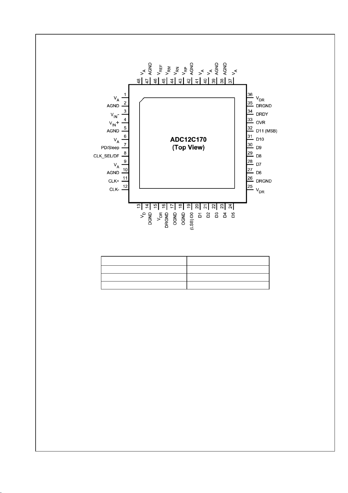
Connection Diagram
20209201
Ordering Information
Industrial (−40°C ≤ TA ≤ +85°C)
Package
ADC12C170CISQ 48 Pin LLP
ADC12C170LFEB Evaluation Board
ADC12C170HFEB Evaluation Board
www.national.com 2
ADC12C170
Page 3
Pin Descriptions and Equivalent Circuits
Pin No. Symbol Equivalent Circuit Description
ANALOG I/O
3
VIN− Differential analog input pins. The differential full-scale input signal
level is two times the reference voltage with each input pin signal
centered on a common mode voltage, VCM.
4
VIN+
43
V
RP
These pins should each be bypassed to AGND with a low ESL
(equivalent series inductance) 0.1 µF capacitor placed very close
to the pin to minimize stray inductance. A 0.1 µF capacitor should
be placed between VRP and VRN as close to the pins as possible,
and a 10 µF capacitor should be placed in parallel.
VRP and VRN should not be loaded. VRM may be loaded to 1mA for
use as a temperature stable 1.5V reference.
It is recommended to use VRM to provide the common mode
voltage, VCM, for the differential analog inputs, VIN+ and VIN−.
45
V
RM
44
V
RN
46
V
REF
This pin can be used as either the +1.0V internal reference voltage
output (internal reference operation) or as the external reference
voltage input (external reference operation).
To use the internal reference, V
REF
should be decoupled to AGND
with a 0.1 µF, low equivalent series inductance (ESL) capacitor. In
this mode, V
REF
defaults as the output for the internal 1.0V
reference.
To use an external reference, overdrive this pin with a low noise
external reference voltage. The input impedance looking into this
pin is 9kΩ. Therefore, to overdrive this pin, the output impedance
of the external reference source should be << 9kΩ.
This pin should not be used to source or sink current.
The full scale differential input voltage range is 2 * V
REF
.
8 CLK_SEL/DF
This is a four-state pin controlling the input clock mode and output
data format.
CLK_SEL/DF = VA, CLK+ and CLK− are configured as a
differential clock input. The output data format is 2's complement.
CLK_SEL/DF = (2/3)*VA, CLK+ and CLK− are configured as a
differential clock input. The output data format is offset binary.
CLK_SEL/DF = (1/3)*VA, CLK+ is configured as a single-ended
clock input and CLK− should be tied to AGND. The output data
format is 2's complement.
CLK_SEL/DF = AGND, CLK+ is configured as a single-ended clock
input and CLK− should be tied to AGND. The output data format is
offset binary.
7 PD/Sleep
This is a three-state input controlling Power Down and Sleep
modes.
PD = VA, Power Down is enabled. In the Power Down state only
the reference voltage circuitry remains active and power
dissipation is reduced.
PD = VA/2, Sleep mode is enabled. Sleep mode is similar to Power
Down mode - it consumes more power but has a faster recovery
time.
PD = AGND, Normal operation.
3 www.national.com
ADC12C170
Page 4
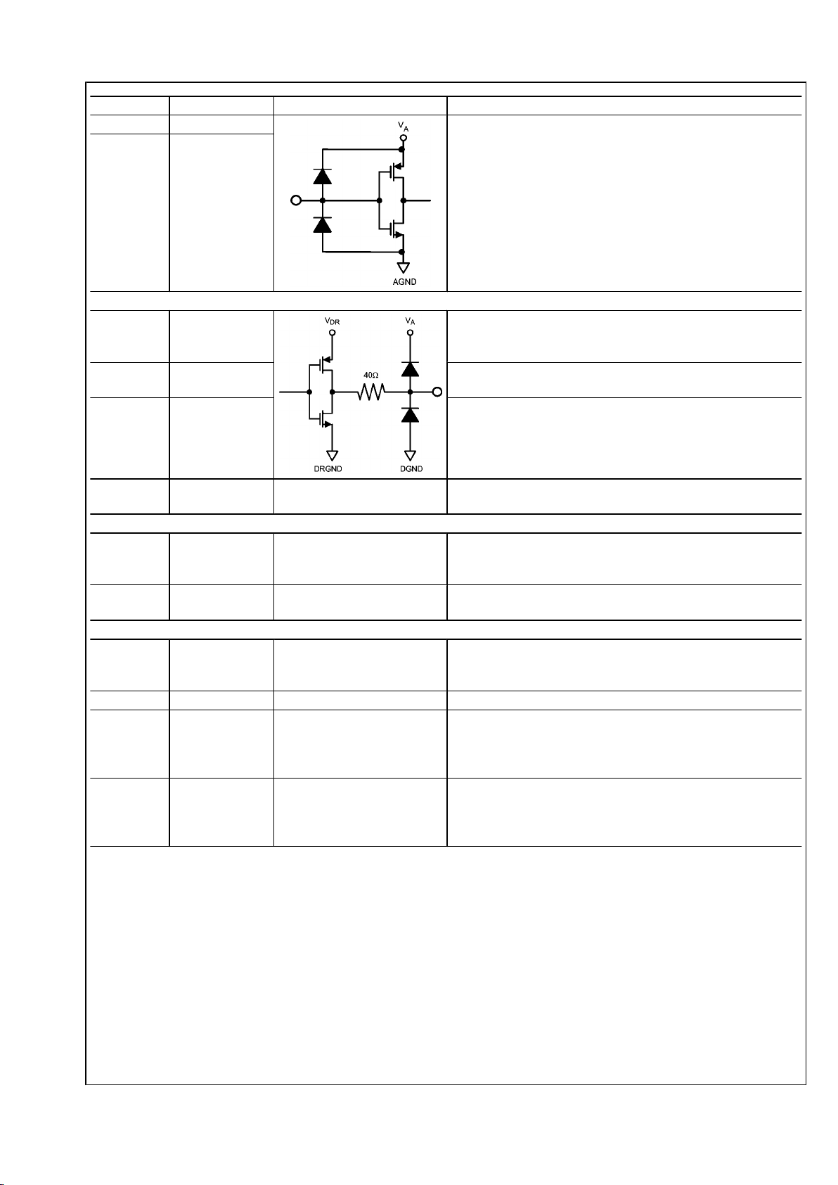
Pin No. Symbol Equivalent Circuit Description
11 CLK+ The clock input pins can be configured to accept either a single-
ended or a differential clock input signal.
When the single-ended clock mode is selected through CLK_SEL/
DF (pin 8), connect the clock input signal to the CLK+ pin and
connect the CLK− pin to AGND.
When the differential clock mode is selected through CLK_SEL/DF
(pin 8), connect the positive and negative clock inputs to the CLK
+ and CLK− pins, respectively.
The analog input is sampled on the falling edge of the clock input.
12 CLK−
DIGITAL I/O
19-24,
27-32
D0–D11
Digital data output pins that make up the 12-Bit conversion result.
D0 (pin 19) is the LSB, while D11 (pin 32) is the MSB of the output
word. Output levels are CMOS compatible.
33 OVR
Over-Range Indicator. This output is set HIGH when the input
amplitude exceeds the 12-Bit conversion range (0 to 4095).
34 DRDY
Data Ready Strobe. This pin is used to clock the output data. It has
the same frequency as the sampling clock. One word of data is
output in each cycle of this signal. The rising edge of this signal
should be used to capture the output data.
17-18 OGND
Output GND, internally tied to GND through 5k ohm resistor to
provide pin compatibility with 14 bit ADCs.
ANALOG POWER
1, 6, 9, 37, 40,
41, 48
V
A
Positive analog supply pins. These pins should be connected to a
quiet +3.3V source and be bypassed to AGND with 0.01 µF and
0.1 µF capacitors located close to the power pins.
2, 5, 10, 38,
39, 42, 47
AGND The ground return for the analog supply.
DIGITAL POWER
13
V
D
Positive digital supply pin. This pin should be connected to a quiet
+3.3V source and be bypassed to DGND with a 0.01 µF and 0.1
µF capacitor located close to the power pin.
14 DGND The ground return for the digital supply.
15, 25, 36
V
DR
Positive driver supply pin for the output drivers. This pin should be
connected to a quiet voltage source of +1.8V and be bypassed to
DRGND with 0.01 µF and 0.1 µF capacitors located close to the
power pins.
16, 26, 35 DRGND
The ground return for the digital output driver supply. These pins
should be connected to the system digital ground, but not be
connected in close proximity to the ADC's DGND or AGND pins.
See Section 6.0 (Layout and Grounding) for more details.
www.national.com 4
ADC12C170
Page 5

Absolute Maximum Ratings
(Notes 1, 2)
If Military/Aerospace specified devices are required,
please contact the National Semiconductor Sales Office/
Distributors for availability and specifications.
Supply Voltage (VA, VD) −0.3V to 4.2V
Supply Voltage (VDR) −0.3V to 2.35V
|VA–VD|
≤ 100 mV
Voltage on Any Input Pin
(Not to exceed 4.2V)
−0.3V to (VA +0.3V)
Voltage on Any Output Pin
(Not to exceed 2.35V)
-0.3V to (VDR +0.2V)
Input Current at Any Pin other
than Supply Pins (Note 3)
±5 mA
Package Input Current (Note 3) ±50 mA
Max Junction Temp (TJ) +150°C
Thermal Resistance (θJA)
24°C/W
Package Dissipation at TA = 25°
C (Note 4)
5.2W
ESD Rating
Human Body Model (Note 5) 2000 V
Machine Model (Note 5) 200 V
Charge Device Model 1000 V
Storage Temperature −65°C to +150°C
Soldering process must comply with National
Semiconductor's Reflow Temperature Profile
specifications. Refer to www.national.com/packaging.
(Note 6)
Operating Ratings (Notes 1, 2)
Operating Temperature
−40°C ≤ TA ≤ +85°C
Supply Voltage (VA, VD) +3.0V to +3.6V
Output Driver Supply (VDR)
+1.6V to +2.0V
CLK −0.05V to (VA + 0.05V)
Clock Duty Cycle 30/70 %
Analog Input Pins 0V to 2.6V
V
CM
1.4V to 1.6V
|AGND-DGND|
≤100mV
5 www.national.com
ADC12C170
Page 6
Converter Electrical Characteristics
Unless otherwise specified, the following specifications apply: VIN = -1dBFS, AGND = DGND = DRGND = 0V, VA = VD = +3.3V,
VDR = +1.8V, Internal V
REF
= +1.0V, f
CLK
= 170 MHz, VCM = VRM, CL = 5 pF/pin, Single-Ended Clock Mode, Offset Binary Format.
Typical values are for TA = 25°C. Boldface limits apply for T
MIN
≤ TA ≤ T
MAX
. All other limits apply for TA = 25°C (Notes 7, 8, 9)
Symbol Parameter Conditions
Typical
(Note 10)
Limits
Units
(Limits)
STATIC CONVERTER CHARACTERISTICS
Resolution with No Missing Codes 12 Bits (min)
INL Integral Non Linearity (Note 11)
±0.85
2.95 LSB (max)
-3.29 LSB (min)
DNL Differential Non Linearity
±0.54
1.3 LSB (max)
-0.92 LSB (min)
PGE Positive Gain Error +0.85
3.38 %FS (max)
-2.10 %FS (min)
NGE Negative Gain Error -0.31
3.00 %FS (max)
-3.57 %FS (min)
TC GE Gain Error Tempco
−40°C ≤ TA ≤ +85°C
+8.0 ppm/°C
V
OFF
Offset Error (VIN+ = VIN−)
−0.13
0.89 %FS (max)
-1.14 %FS (min)
TC V
OFF
Offset Error Tempco
−40°C ≤ TA ≤ +85°C
+0.5 ppm/°C
Under Range Output Code 0 0
Over Range Output Code 4095 4095
REFERENCE AND ANALOG INPUT CHARACTERISTICS
V
CM
Common Mode Input Voltage 1.5 V
V
RM
Reference Ladder Midpoint Output
Voltage
Output load = 1 mA 1.5 V
C
IN
VIN Input Capacitance (each pin to GND)
(Note 12)
VIN = 1.5 Vdc
± 0.5 V
(CLK LOW) 9 pF
(CLK HIGH) 6 pF
V
REF
Reference Voltage (Note 13) 1.00 V
Reference Input Resistance 9
kΩ
www.national.com 6
ADC12C170
Page 7
Dynamic Converter Electrical Characteristics
Unless otherwise specified, the following specifications apply: VIN = -1dBFS, AGND = DGND = DRGND = 0V, VA = VD = +3.3V,
VDR = +1.8V, Internal V
REF
= +1.0V, f
CLK
= 170 MHz, VCM = VRM, CL = 5 pF/pin, Single-Ended Clock Mode, Offset Binary Format.
Typical values are for TA = 25°C. Boldface limits apply for T
MIN
≤ TA ≤ T
MAX
. All other limits apply for TA = 25°C (Notes 7, 8, 9)
Symbol Parameter Conditions
Typical
(Note
10)
Limits
Units
(Limits)
DYNAMIC CONVERTER CHARACTERISTICS, AIN = -1dBFS
FPBW Full Power Bandwidth -1 dBFS Input, −3 dB Corner 1.1 GHz
SNR Signal-to-Noise Ratio
fIN = 10 MHz
67.5 dBFS
fIN = 70 MHz
67.2 66.0 dBFS
fIN = 150 MHz
67.1 dBFS
fIN = 250 MHz
66.8 dBFS
fIN = 400 MHz
66.0 dBFS
SFDR Spurious Free Dynamic Range
fIN = 10 MHz
86.6 dBFS
fIN = 70 MHz
85.4 74.0 dBFS
fIN = 150 MHz
83.4 dBFS
fIN = 250 MHz
84.1 dBFS
fIN = 400 MHz
72.9 dBFS
ENOB Effective Number of Bits
fIN = 10 MHz
10.9 Bits
fIN = 70 MHz
10.8 10.5 Bits
fIN = 150 MHz
10.8 Bits
fIN = 250 MHz
10.8 Bits
fIN = 400 MHz
10.5 Bits
THD Total Harmonic Disortion
fIN = 10 MHz
-82.6 dBFS
fIN = 70 MHz
−82.6 -72.0 dBFS
fIN = 150 MHz
-81.1 dBFS
fIN = 250 MHz
-80.3 dBFS
fIN = 400 MHz
-70.7 dBFS
H2 Second Harmonic Distortion
fIN = 10 MHz
-89.7 dBFS
fIN = 70 MHz
−88.4 -77.0 dBFS
fIN = 150 MHz
-93.5 dBFS
fIN = 250 MHz
-91.0 dBFS
fIN = 400 MHz
-72.9 dBFS
H3 Third Harmonic Distortion
fIN = 10 MHz
-86.7 dBFS
fIN = 70 MHz
−85.4 -74 dBFS
fIN = 150 MHz
-84.6 dBFS
fIN = 250 MHz
-84.1 dBFS
fIN = 400 MHz
-77.6 dBFS
SINAD Signal-to-Noise and Distortion Ratio
fIN = 10 MHz
67.3 dBFS
fIN = 70 MHz
67.1 65.2 dBFS
fIN = 150 MHz
67.0 dBFS
fIN = 250 MHz
66.6 dBFS
fIN = 400 MHz
64.7 dBFS
7 www.national.com
ADC12C170
Page 8

Logic and Power Supply Electrical Characteristics
Unless otherwise specified, the following specifications apply: VIN = -1 dBFS, AGND = DGND = DRGND = 0V, VA = VD = +3.3V,
VDR = +1.8V, Internal V
REF
= +1.0V, f
CLK
= 170 MHz, VCM = VRM, CL = 5 pF/pin, Single-Ended Clock Mode, Offset Binary Format.
Typical values are for TA = 25°C. Boldface limits apply for T
MIN
≤ TA ≤ T
MAX
. All other limits apply for TA = 25°C (Notes 7, 8, 9)
Symbol Parameter Conditions
Typical
(Note 10)
Limits
Units
(Limits)
CLK INPUT CHARACTERISTICS
V
IN(1)
Logical “1” Input Voltage
VD = 3.6V
2.0 V (min)
V
IN(0)
Logical “0” Input Voltage
VD = 3.0V
0.8 V (max)
I
IN(1)
Logical “1” Input Current
VIN = 3.3V
10
µA
I
IN(0)
Logical “0” Input Current VIN = 0V
−10 µA
C
IN
Input Capacitance 5 pF
DIGITAL OUTPUT CHARACTERISTICS (D0–D11, DRDY, OVR)
V
OUT(1)
Logical “1” Output Voltage
I
OUT
= −0.5 mA , VDR = 1.8V
1.2 V (min)
V
OUT(0)
Logical “0” Output Voltage
I
OUT
= 1.6 mA, VDR = 1.8V
0.4 V (max)
+I
SC
Output Short Circuit Source Current V
OUT
= 0V
−10
mA
−I
SC
Output Short Circuit Sink Current
V
OUT
= V
DR
10 mA
C
OUT
Digital Output Capacitance 5 pF
POWER SUPPLY CHARACTERISTICS
I
A
Analog Supply Current
Full Operation 207 259 mA (max)
I
D
Digital Supply Current
Full Operation 9.8 10.7 mA (max)
I
DR
Digital Output Supply Current
Full Operation (Note 14) 13 mA
Power Consumption
Excludes IDR (Note 14) 715 mW
Power Down Power Consumption 5 mW
Sleep Power Consumption 50 mW
www.national.com 8
ADC12C170
Page 9

Timing and AC Characteristics
Unless otherwise specified, the following specifications apply: VIN = -1dBFS, AGND = DGND = DRGND = 0V, VA = VD = +3.3V,
VDR = +1.8V, Internal V
REF
= +1.0V, f
CLK
= 170 MHz, VCM = VRM, CL = 5 pF/pin, Single-Ended Clock Mode, Offset Binary Format.
Typical values are for TA = 25°C. Timing measurements are taken at 50% of the signal amplitude. Boldface limits apply for
T
MIN
≤ TA ≤ T
MAX
. All other limits apply for TA = 25°C (Notes 7, 8, 9)
Symbol Parameter Conditions
Typical
(Note 10)
Limits
Units
(Limits)
Maximum Clock Frequency 170 MHz (max)
Minimum Clock Frequency 5 MHz (min)
t
CH
Clock High Time 2.7
ns
t
CL
Clock Low Time
2.7 ns
Conversion Latency 7 Clock Cycles
t
OD
Output Delay of CLK to DATA Relative to falling edge of CLK 2.0 ns
t
DV
Data Output Setup Time
Time output data is valid before the
output edge of DRDY (Note 15)
1.9 1.35 ns (min)
t
DNV
Data Output Hold Time
Time till output data is not valid after the
output edge of DRDY (Note 15)
1.9 1.35 ns (min)
t
AD
Aperture Delay 0.5 ns
Aperture Jitter 0.08 ps rms
Power Down Recovery Time
0.1 µF on pins 43, 44; 10 µF and 0.1 µF
between pins 43, 44; 0.1 µF and 10 µF
on pins 45, 46
3.0 ms
Sleep Recovery Time
0.1 µF on pins 43, 44; 10 µF and 0.1 µF
between pins 43, 44; 0.1 µF and 10 µF
on pins 45, 46
100 µs
Note 1: Absolute Maximum Ratings indicate limits beyond which damage to the device may occur. Operating Ratings indicate conditions for which the device is
guaranteed to be functional, but do not guarantee specific performance limits. For guaranteed specifications and test conditions, see the Electrical Characteristics.
The guaranteed specifications apply only for the test conditions listed. Some performance characteristics may degrade when the device is not operated under
the listed test conditions. Operation of the device beyond the maximum Operating Ratings is not recommended.
Note 2: All voltages are measured with respect to GND = AGND = DGND = DRGND = 0V, unless otherwise specified.
Note 3: When the input voltage at any pin exceeds the power supplies (that is, VIN < AGND, or VIN > VA), the current at that pin should be limited to ±5 mA. The
±50 mA maximum package input current rating limits the number of pins that can safely exceed the power supplies with an input current of ±5 mA to 10.
Note 4: The maximum allowable power dissipation is dictated by T
J,max
, the junction-to-ambient thermal resistance, (θJA), and the ambient temperature, (TA), and
can be calculated using the formula P
D,max
= (T
J,max
- TA )/θJA. The values for maximum power dissipation listed above will be reached only when the device is
operated in a severe fault condition (e.g. when input or output pins are driven beyond the power supply voltages, or the power supply polarity is reversed). Such
conditions should always be avoided.
Note 5: Human Body Model is 100 pF discharged through a 1.5 kΩ resistor. Machine Model is 220 pF discharged through 0 Ω
Note 6: Reflow temperature profiles are different for lead-free and non-lead-free packages.
Note 7: The inputs are protected as shown below. Input voltage magnitudes above VA or below GND will not damage this device, provided current is limited per
(Note 3). However, errors in the A/D conversion can occur if the input goes above 2.6V or below GND as described in the Operating Ratings section.
20209211
Note 8: To guarantee accuracy, it is required that |VA–VD| ≤ 100 mV and separate bypass capacitors are used at each power supply pin.
Note 9: With the test condition for V
REF
= +1.0V (2V
P-P
differential input), the 12-Bit LSB is 488.3 µV.
Note 10: Typical figures are at TA = 25°C and represent most likely parametric norms at the time of product characterization. The typical specifications are not
guaranteed.
Note 11: Integral Non Linearity is defined as the deviation of the analog value, expressed in LSBs, from the straight line that passes through positive and negative
full-scale.
Note 12: The input capacitance is the sum of the package/pin capacitance and the sample and hold circuit capacitance.
Note 13: Optimum performance will be obtained by keeping the reference input in the 0.9V to 1.1V range. The LM4051CIM3-ADJ (SOT-23 package) is
recommended for external reference applications.
Note 14: IDR is the current consumed by the switching of the output drivers and is primarily determined by load capacitance on the output pins, the supply voltage,
VDR, and the rate at which the outputs are switching (which is signal dependent). IDR=VDR(C0 x f0 + C1 x f1 +....C11 x f11) where VDR is the output driver power
supply voltage, Cn is total capacitance on the output pin, and fn is the average frequency at which that pin is toggling.
Note 15: This test parameter is guaranteed by design and characterization.
9 www.national.com
ADC12C170
Page 10

Specification Definitions
APERTURE DELAY is the time after the falling edge of the
clock to when the input signal is acquired or held for conversion.
APERTURE JITTER (APERTURE UNCERTAINTY) is the
variation in aperture delay from sample to sample. Aperture
jitter manifests itself as noise in the output.
CLOCK DUTY CYCLE is the ratio of the time during one cycle
that a repetitive digital waveform is high to the total time of
one period. The specification here refers to the ADC clock
input signal.
COMMON MODE VOLTAGE (VCM) is the common DC voltage applied to both input terminals of the ADC.
CONVERSION LATENCY is the number of clock cycles between initiation of conversion and when that data is presented
to the output driver stage. Data for any given sample is available at the output pins the Pipeline Delay plus the Output
Delay after the sample is taken. New data is available at every
clock cycle, but the data lags the conversion by the pipeline
delay.
DIFFERENTIAL NON-LINEARITY (DNL) is the measure of
the maximum deviation from the ideal step size of 1 LSB.
EFFECTIVE NUMBER OF BITS (ENOB, or EFFECTIVE
BITS) is another method of specifying Signal-to-Noise and
Distortion Ratio or SINAD. ENOB is defined as (SINAD -
1.76) / 6.02 and says that the converter is equivalent to a
perfect ADC of this (ENOB) number of bits.
FULL POWER BANDWIDTH is a measure of the frequency
at which the reconstructed output fundamental drops 3 dB
below its low frequency value for a full scale input.
GAIN ERROR is the deviation from the ideal slope of the
transfer function. It can be calculated as:
Gain Error = Positive Full Scale Error − Negative Full Scale
Error
It can also be expressed as Positive Gain Error and Negative
Gain Error, which are calculated as:
PGE = Positive Full Scale Error - Offset Error
NGE = Offset Error - Negative Full Scale Error
INTEGRAL NON LINEARITY (INL) is a measure of the deviation of each individual code from a line drawn from negative
full scale (½ LSB below the first code transition) through positive full scale (½ LSB above the last code transition). The
deviation of any given code from this straight line is measured
from the center of that code value.
INTERMODULATION DISTORTION (IMD) is the creation of
additional spectral components as a result of two sinusoidal
frequencies being applied to the ADC input at the same time.
It is defined as the ratio of the power in the intermodulation
products to the total power in the original frequencies. IMD is
usually expressed in dBFS.
LSB (LEAST SIGNIFICANT BIT) is the bit that has the smallest value or weight of all bits. This value is VFS/2n, where
“VFS” is the full scale input voltage and “n” is the ADC resolution in bits.
MISSING CODES are those output codes that will never appear at the ADC outputs. The ADC12C170 is guaranteed not
to have any missing codes.
MSB (MOST SIGNIFICANT BIT) is the bit that has the largest
value or weight. Its value is one half of full scale.
NEGATIVE FULL SCALE ERROR is the difference between
the actual first code transition and its ideal value of ½ LSB
above negative full scale.
OFFSET ERROR is the difference between the two input
voltages [(VIN+) – (VIN-)] required to cause a transition from
code 2047 to 2048.
OUTPUT DELAY is the time delay after the falling edge of the
clock before the data update is presented at the output pins.
PIPELINE DELAY (LATENCY) See CONVERSION LATENCY.
POSITIVE FULL SCALE ERROR is the difference between
the actual last code transition and its ideal value of 1½ LSB
below positive full scale.
POWER SUPPLY REJECTION RATIO (PSRR) is a measure
of how well the ADC rejects a change in the power supply
voltage. PSRR is the ratio of the Full-Scale output of the ADC
with the supply at the minimum DC supply limit to the FullScale output of the ADC with the supply at the maximum DC
supply limit, expressed in dB.
SIGNAL TO NOISE RATIO (SNR) is the ratio, expressed in
dB, of the rms value of the input signal to the rms value of the
sum of all other spectral components below one-half the sampling frequency, not including harmonics or DC.
SIGNAL TO NOISE PLUS DISTORTION (S/N+D or
SINAD) Is the ratio, expressed in dB, of the rms value of the
input signal to the rms value of all of the other spectral components below half the clock frequency, including harmonics
but excluding d.c.
SPURIOUS FREE DYNAMIC RANGE (SFDR) is the difference, expressed in dB, between the rms values of the input
signal and the peak spurious signal, where a spurious signal
is any signal present in the output spectrum that is not present
at the input.
TOTAL HARMONIC DISTORTION (THD) is the ratio, expressed in dB, of the rms total of the first nine harmonic levels
at the output to the level of the fundamental at the output. THD
is calculated as
where f1 is the RMS power of the fundamental (output) frequency and f2 through f10 are the RMS power of the first 9
harmonic frequencies in the output spectrum.
SECOND HARMONIC DISTORTION (2ND HARM) is the difference expressed in dB, between the RMS power in the input
frequency at the output and the power in its 2nd harmonic
level at the output.
THIRD HARMONIC DISTORTION (3RD HARM) is the difference, expressed in dB, between the RMS power in the
input frequency at the output and the power in its 3rd harmonic
level at the output.
www.national.com 10
ADC12C170
Page 11

Timing Diagram
20209209
Output Timing
Transfer Characteristic
20209210
FIGURE 1. Transfer Characteristic (Offset Binary Format)
11 www.national.com
ADC12C170
Page 12

Typical Performance Characteristics, DNL, INL
Unless otherwise specified, the following specifications apply: VIN = -1dBFS, AGND = DGND = DRGND = 0V, VA = VD = +3.3V,
VDR = +1.8V, Internal V
REF
= +1.0V, f
CLK
= 170 MHz, VCM = VRM, CL = 5 pF/pin, Single-Ended Clock Mode, Offset Binary Format.
Typical values are for TA = 25°C. (Notes 7, 8, 9)
DNL
20209261
INL
20209262
www.national.com 12
ADC12C170
Page 13

Typical Performance Characteristics, Dynamic Performance
Unless otherwise specified, the following specifications apply: VIN = -1dBFS, AGND = DGND = DRGND = 0V, VA = VD = +3.3V,
VDR = +1.8V, Internal V
REF
= +1.0V, f
CLK
= 170 MHz, fIN = 70 MHz, VCM = VRM, CL = 5 pF/pin, Single-Ended Clock Mode, Offset
Binary Format. Typical values are for TA = 25°C.
SNR, SINAD, SFDR vs. f
IN
20209295
DISTORTION vs. f
IN
20209283
SNR, SINAD, SFDR vs. V
A
20209273
DISTORTION vs. V
A
20209274
SNR, SINAD, SFDR vs. V
DR
20209275
DISTORTION vs. V
DR
20209276
13 www.national.com
ADC12C170
Page 14

Typical Performance Characteristics, Dynamic Performance
Unless otherwise specified, the following specifications apply: VIN = -1dBFS, AGND = DGND = DRGND = 0V, VA = VD = +3.3V,
VDR = +1.8V, Internal V
REF
= +1.0V, f
CLK
= 170 MHz, fIN = 70 MHz, VCM = VRM, CL = 5 pF/pin, Single-Ended Clock Mode, Offset
Binary Format. Typical values are for TA = 25°C.
SNR, SINAD, SFDR vs. V
REF
20209277
DISTORTION vs. V
REF
20209278
SNR, SINAD, SFDR vs. Temperature
20209281
DISTORTION vs. Temperature
20209282
www.national.com 14
ADC12C170
Page 15

Typical Performance Characteristics, Dynamic Performance
Unless otherwise specified, the following specifications apply: VIN = -1dBFS, AGND = DGND = DRGND = 0V, VA = VD = +3.3V,
VDR = +1.8V, Internal V
REF
= +1.0V, f
CLK
= 170 MHz, fIN = 70 MHz, VCM = VRM, CL = 5 pF/pin, Single-Ended Clock Mode, Offset
Binary Format. Typical values are for TA = 25°C.
Spectral Response @ 70 MHz Input
20209292
Spectral Response @ 150 MHz Input
20209293
Spectral Response @ 220 MHz Input
20209294
Spectral Response @ 250 MHz Input
20209296
Spectral Response @ 350 MHz Input
20209297
Spectral Response @ 400 MHz Input
20209298
15 www.national.com
ADC12C170
Page 16

Functional Description
Operating on dual +3.3V and +1.8V supplies, the ADC12C170 digitizes a differential analog input signal to 12 bits,
using a differential pipelined architecture with error correction
circuitry and an on-chip sample-and-hold circuit to ensure
maximum performance.
The user has the choice of using an internal 1.0V stable reference, or using an external reference. The ADC12C170 will
accept an external reference between 0.9V and 1.1V (1.0V
recommended) which is buffered on-chip to ease the task of
driving that pin. The +1.8V output driver supply reduces power consumption and decreases the noise at the output of the
converter.
The quad state function pin CLK_SEL/DF (pin 8) allows the
user to choose between using a single-ended or a differential
clock input and between offset binary or 2's complement output data format. The digital outputs are CMOS compatible
signals that are clocked by a synchronous data ready output
signal (DRDY, pin 34) at the same rate as the clock input. For
the ADC12C170 the clock frequency can be between 5 MSPS
and 170 MSPS (typical) with fully specified performance at
170 MSPS. The analog input is acquired at the falling edge of
the clock and the digital data for a given sample is output on
the falling edge of the DRDY signal and is delayed by the
pipeline for 7 clock cycles. The data should be captured on
the rising edge of the DRDY signal.
Power-down is selectable using the PD/Sleep pin (pin 7). A
logic high on the PD/Sleep pin disables everything except the
voltage reference circuitry and reduces the converter power
consumption to 5 mW. When PD/Sleep is biased to VA/2 the
the chip enters sleep mode. In sleep mode everything except
the voltage reference circuitry and its accompanying on chip
buffer is disabled; power consumption is reduced to 50 mW.
For normal operation, the PD/Sleep pin should be connected
to the analog ground (AGND). A duty cycle stabilizer maintains performance over a wide range of clock duty cycles.
Applications Information
1.0 OPERATING CONDITIONS
We recommend that the following conditions be observed for
operation of the ADC12C170:
3.0V ≤ VA ≤ 3.6V
VD = V
A
VDR = 1.8V
5 MHz ≤ f
CLK
≤ 170 MHz
1.0V internal reference
0.9V ≤ V
REF
≤ 1.1V (for an external reference)
VCM = 1.5V (from VRM)
Single Ended Clock Mode
2.0 ANALOG INPUTS
2.1 Signal Inputs
2.1.1 Differential Analog Input Pins
The ADC12C170 has one pair of analog signal input pins,
VIN+ and VIN−, which form a differential input pair. The input
signal, VIN, is defined as
VIN = (VIN+) – (VIN−)
Figure 2 shows the expected input signal range. Note that the
common mode input voltage, VCM, should be 1.5V. Using
VRM (pin 45) for VCM will ensure the proper input common
mode level for the analog input signal. The peaks of the individual input signals should each never exceed 2.6V. Each
analog input pin of the differential pair should have a peak-topeak voltage equal to the reference voltage, V
REF
, be 180°
out of phase with each other and be centered around
VCM.The peak-to-peak voltage swing at each analog input pin
should not exceed the value of the reference voltage or the
output data will be clipped.
20209214
FIGURE 2. Expected Input Signal Range
For single frequency sine waves the full scale error in LSB
can be described as approximately
EFS = 4096 ( 1 - sin (90° + dev))
Where dev is the angular difference in degrees between the
two signals having a 180° relative phase relationship to each
other (see Figure 3). For single frequency inputs, angular errors result in a reduction of the effective full scale input. For
complex waveforms, however, angular errors will result in
distortion.
20209216
FIGURE 3. Angular Errors Between the Two Input Signals
Will Reduce the Output Level or Cause Distortion
It is recommended to drive the analog inputs with a source
impedance less than 100Ω. Matching the source impedance
for the differential inputs will improve even ordered harmonic
performance (particularly second harmonic).
Table 1 indicates the input to output relationship of the ADC12C170.
www.national.com 16
ADC12C170
Page 17

TABLE 1. Input to Output Relationship
V
IN
+
V
IN
−
Binary Output 2’s Complement Output
VCM − V
REF
/2 VCM + V
REF
/2
0000 0000 0000 1000 0000 0000 Negative Full-Scale
VCM − V
REF
/4 VCM + V
REF
/4
0100 0000 0000 1100 0000 0000
V
CM
V
CM
1000 0000 0000 0000 0000 0000 Mid-Scale
VCM + V
REF
/4 VCM − V
REF
/4
1100 0000 0000 0100 0000 0000
VCM + V
REF
/2 VCM − V
REF
/2
1111 1111 1111 0111 1111 1111 Positive Full-Scale
2.1.2 Driving the Analog Inputs
The VIN+ and the VIN− inputs of the ADC12C170 have an internal sample-and-hold circuit which consists of an analog
switch followed by a switched-capacitor amplifier. The analog
inputs are connected to the sampling capacitors through
NMOS switches, and each analog input has parasitic capacitances associated with it.
When the clock is high, the converter is in the sample phase.
The analog inputs are connected to the sampling capacitor
through the NMOS switches, which causes the capacitance
at the analog input pins to appear as the pin capacitance plus
the internal sample and hold circuit capacitance (approximately 9 pF). While the clock level remains high, the sampling
capacitor will track the changing analog input voltage. When
the clock transitions from high to low, the converter enters the
hold phase, during which the analog inputs are disconnected
from the sampling capacitor. The last voltage that appeared
at the analog input before the clock transition will be held on
the sampling capacitor and will be sent to the ADC core. The
capacitance seen at the analog input during the hold phase
appears as the sum of the pin capacitance and the parasitic
capacitances associated with the sample and hold circuit of
each analog input (approximately 6 pF). Once the clock signal
transitions from low to high, the analog inputs will be reconnected to the sampling capacitor to capture the next sample.
Usually, there will be a difference between the held voltage
on the sampling capacitor and the new voltage at the analog
input. This will cause a charging glitch that is proportional to
the voltage difference between the two samples to appear at
the analog input pin. The input circuitry must be fast enough
to allow the sampling capacitor to settle before the clock signal goes low again, as incomplete settling can degrade the
SFDR performance.
A single-ended to differential conversion circuit is shown in
Figure 4. A transformer is preferred for high frequency input
signals. Terminating the transformer on the secondary side
provides two advantages. First, it presents a real broadband
impedance to the ADC inputs and second, it provides a common path for the charging glitches from each side of the
differential sample-and-hold circuit.
One short-coming of using a transformer to achieve the single-ended to differential conversion is that most RF transformers have poor low frequency performance. A differential
amplifier can be used to drive the analog inputs for low frequency applications. The amplifier must be fast enough to
settle from the charging glitches on the analog input resulting
from the sample-and-hold operation before the clock goes
high and the sample is passed to the ADC core.
The SFDR performance of the converter depends on the external signal conditioning circuity used, as this affects how
quickly the sample-and-hold charging glitch will settle. An external resistor and capacitor network as shown in Figure 4
should be used to isolate the charging glitches at the ADC
input from the external driving circuit and to filter the wideband
noise at the converter input. These components should be
placed close to the ADC inputs because the analog input of
the ADC is the most sensitive part of the system, and this is
the last opportunity to filter that input. For Nyquist applications
the RC pole should be at the ADC sample rate. The ADC input
capacitance in the sample mode should be considered when
setting the RC pole. For wideband undersampling applications, the RC pole should be set at about 1.5 to 2 times the
maximum input frequency to maintain a linear delay response.
2.1.3 Input Common Mode Voltage
The input common mode voltage, VCM, should be in the range
of 1.4V to 1.6V and be a value such that the peak excursions
of the analog signal do not go more negative than ground or
more positive than 2.6V. It is recommended to use VRM (pin
45) as the input common mode voltage.
2.2 Reference Pins
The ADC12C170 is designed to operate with an internal 1.0V
reference, or an external 1.0V reference, but performs well
with external reference voltages in the range of 0.9V to 1.1V.
The internal 1.0 Volt reference is the default condition when
no external reference input is applied to the V
REF
pin. If a volt-
age in the range of 0.9V to 1.1V is applied to the V
REF
pin,
then that voltage is used for the reference. The V
REF
pin
should always be bypassed to ground with a 0.1 µF capacitor
close to the reference input pin. Lower reference voltages will
decrease the signal-to-noise ratio (SNR) of the ADC12C170.
Increasing the reference voltage (and the input signal swing)
beyond 1.1V may degrade THD for a full-scale input, especially at higher input frequencies.
It is important that all grounds associated with the reference
voltage and the analog input signal make connection to the
ground plane at a single, quiet point to minimize the effects of
noise currents in the ground path.
The Reference Bypass Pins (VRP, VRM, and VRN) are made
available for bypass purposes. All these pins should each be
bypassed to ground with a 0.1 µF capacitor. A 0.1 µF and a
10 µF capacitor should be placed between the VRP and V
RN
pins, as shown in Figure 4. This configuration is necessary to
avoid reference oscillation, which could result in reduced SFDR and/or SNR. VRM may be loaded to 1mA for use as a
temperature stable 1.5V reference. The remaining pins
should not be loaded.
Smaller capacitor values than those specified will allow faster
recovery from the power down and sleep modes, but may result in degraded noise performance. Loading any of these
pins, other than VRM, may result in performance degradation.
The nominal voltages for the reference bypass pins are as
follows:
VRM = 1.5 V
VRP = VRM + V
REF
/ 2
VRN = VRM − V
REF
/ 2
17 www.national.com
ADC12C170
Page 18

2.3 Control Inputs
2.3.1 Power-Down & Sleep (PD/Sleep)
The power-down and sleep modes can be enabled through
this three-state input pin. Table 2 shows how to utilize these
options.
TABLE 2. Power Down/Sleep Selection Table
PD Input Voltage Power State
V
A
Power-down
VA/2
Sleep
AGND On
The power-down and sleep modes allows the user to conserve power when the converter is not being used. In the
power-down state all bias currents of the analog circuitry, excluding the reference are shut down which reduces the power
consumption to 5 mW with no clock running. In sleep mode
some additional buffer circuitry is left on to allow an even
faster wake time; power consumption in the sleep mode is 50
mW with no clock running. In both of these modes the output
data pins are undefined and the data in the pipeline is corrupted.
The Exit Cycle time for both the sleep and power-down mode
is determined by the value of the capacitors on the VRP, V
RM
and VRN reference bypass pins (pins 43, 44 and 45). These
capacitors lose their charge when the ADC is not operating
and must be recharged by on-chip circuitry before conversions can be accurate. For power-down mode the Exit Cycle
time is about 3 ms with the recommended component values.
The Exit Cycle time is faster for sleep mode. Smaller capacitor
values allow slightly faster recovery from the power down and
sleep mode, but can result in a reduction in SNR, SINAD and
ENOB performance.
2.3.2 Clock Mode Select/Data Format (CLK_SEL/DF)
Single-ended versus differential clock mode and output data
format are selectable using this quad-state function pin. Table
3 shows how to select between the clock modes and the output data formats.
TABLE 3. Clock Mode and Data Format Selection Table
CLK_SEL/DF
Input Voltage
Clock Mode
Output Data
Format
V
A
Differential 2's Complement
(2/3) * V
A
Differential Offset Binary
(1/3) * V
A
Single-Ended 2's Complement
AGND Single-Ended Offset Binary
3.0 CLOCK INPUTS
The CLK+ and CLK− signals control the timing of the sampling
process. The CLK_SEL/DF pin (pin 8) allows the user to configure the ADC for either differential or single-ended clock
mode (see Section 3.3). In differential clock mode, the two
clock signals should be exactly 180° out of phase from each
other and of the same amplitude. In the single-ended clock
mode, the clock signal should be routed to the CLK+ input and
the CLK− input should be tied to AGND in combination with
the correct setting from Table 3.
To achieve the optimum noise performance, the clock inputs
should be driven with a stable, low jitter clock signal in the
range indicated in the Electrical Table. The clock input signal
should also have a short transition region. This can be
achieved by passing a low-jitter sinusoidal clock source
through a high speed buffer gate. This configuration is shown
in Figure 4. The trace carrying the clock signal should be as
short as possible and should not cross any other signal line,
analog or digital, not even at 90°. Figure 4 shows the recom-
mended clock input circuit.
The clock signal also drives an internal state machine. If the
clock is interrupted, or its frequency is too low, the charge on
the internal capacitors can dissipate to the point where the
accuracy of the output data will degrade. This is what limits
the minimum sample rate.
The clock line should be terminated at its source in the characteristic impedance of that line. Take care to maintain a
constant clock line impedance throughout the length of the
line. Refer to Application Note AN-905 for information on setting characteristic impedance.
It is highly desirable that the the source driving the ADC clock
pins only drive that pin. However, if that source is used to drive
other devices, then each driven pin should be AC terminated
with a series RC to ground, such that the resistor value is
equal to the characteristic impedance of the clock line and the
capacitor value is
where tPD is the signal propagation rate down the clock line,
"L" is the line length and ZO is the characteristic impedance
of the clock line. This termination should be as close as possible to the ADC clock pin but beyond it as seen from the clock
source. Typical tPD is about 150 ps/inch (60 ps/cm) on FR-4
board material. The units of "L" and tPD should be the same
(inches or centimeters).
The duty cycle of the clock signal can affect the performance
of the A/D Converter. Because achieving a precise duty cycle
is difficult, the ADC12C170 has a Duty Cycle Stabilizer. It is
designed to maintain performance over a clock duty cycle
range of 30% to 70%.
4.0 DIGITAL OUTPUTS
Digital outputs consist of the 1.8V CMOS signals D0-D11,
DRDY, OVR and OGND.
The ADC12C170 has 16 CMOS compatible data output pins:
12 data output bits corresponding to the converted input value, a data ready (DRDY) signal that should be used to capture
the output data, an over-range indicator (OVR) which is set
high when the sample amplitude exceeds the 12-Bit conversion range and two output ground pins (OGND) which should
be ignored except when used for compatibility with a 14 bit
part. Valid data is present at these outputs while the PD/Sleep
pin is low.
Data should be captured and latched with the rising edge of
the DRDY signal. Depending on the setup and hold time requirements of the receiving circuit (ASIC), either the rising
edge or the falling edge of the DRDY signal can be used to
latch the data. Generally, rising-edge capture would maximize setup time with minimal hold time; while falling-edgecapture would maximize hold time with minimal setup time.
However, actual timing for the falling-edge case depends
greatly on the CLK frequency and both cases also depend on
the delays inside the ASIC. Refer to the AC Electrical Characterisitics table.
Be very careful when driving a high capacitance bus. The
more capacitance the output drivers must charge for each
conversion, the more instantaneous digital current flows
through VDR and DRGND. These large charging current
www.national.com 18
ADC12C170
Page 19

spikes can cause on-chip ground noise and couple into the
analog circuitry, degrading dynamic performance. Adequate
bypassing, limiting output capacitance and careful attention
to the ground plane will reduce this problem. Additionally, bus
capacitance beyond the specified 5 pF/pin will cause tOD to
increase, reducing the setup and hold time of the ADC output
data. The result could be an apparent reduction in dynamic
performance.
To minimize noise due to output switching, the load currents
at the digital outputs should be minimized. This can be done
by using a programmable logic device (PLD) such as the
LC4032V-25TN48C to level translate the ADC output data
from 1.8V to 3.3V for use by any other circuitry. Only one load
should be connected to each output pin. The outputs of the
ADC14155 have 40Ω on-chip series resistors to limit the output currents at the digital outputs. Additionally, inserting series resistors of about 22Ω at the digital outputs, close to the
ADC pins, will isolate the outputs from trace and other circuit
capacitances and limit the output currents, which could otherwise result in performance degradation. See Figure 4.
20209213
FIGURE 4. Application Circuit using Transformer Drive Circuit (If 14-bit compatibility is not required do not connect pins
17 and 18)
5.0 POWER SUPPLY CONSIDERATIONS
The power supply pins should be bypassed with a 0.1 µF capacitor and with a 0.01 µF ceramic chip capacitor close to
each power pin. Leadless chip capacitors are preferred because they have low series inductance.
As is the case with all high-speed converters, the ADC12C170 is sensitive to power supply noise. Accordingly, the
noise on the analog supply pin should be kept below 100
mV
P-P
.
No pin should ever have a voltage on it that is in excess of the
supply voltages, not even on a transient basis. Be especially
careful of this during power turn on and turn off.
The VDR pin provides power for the output drivers and may be
operated from a supply in the range of 1.6V to 2.0V. This enables lower power operation, reduces the noise coupling
effects from the digital outputs to the analog circuitry and simplifies interfacing to lower voltage devices and systems. Note,
however, that tOD increases with reduced VDR. A level translator may be required to interface the digital output signals of
the ADC12C170 to non-1.8V CMOS devices.
6.0 LAYOUT AND GROUNDING
Proper grounding and proper routing of all signals are essential to ensure accurate conversion. Maintaining separate analog and digital areas of the board, with the ADC12C170
between these areas, is required to achieve specified performance.
The ground return for the data outputs (DRGND) carries the
ground current for the output drivers. The output current can
exhibit high transients that could add noise to the conversion
process. To prevent this from happening, the DRGND pins
should NOT be connected to system ground in close proximity
to any of the ADC12C170's other ground pins.
Capacitive coupling between the typically noisy digital circuitry and the sensitive analog circuitry can lead to poor performance. The solution is to keep the analog circuitry separated
from the digital circuitry, and to keep the clock line as short as
possible.
The effects of the noise generated from the ADC output
switching can be minimized through the use of 22Ω resistors
in series with each data output line. Locate these resistors as
close to the ADC output pins as possible.
Since digital switching transients are composed largely of
high frequency components, total ground plane copper
weight will have little effect upon the logic-generated noise.
This is because of the skin effect. Total surface area is more
important than is total ground plane area.
Generally, analog and digital lines should cross each other at
90° to avoid crosstalk. To maximize accuracy in high speed,
high resolution systems, however, avoid crossing analog and
digital lines altogether. It is important to keep clock lines as
19 www.national.com
ADC12C170
Page 20

short as possible and isolated from ALL other lines, including
other digital lines. Even the generally accepted 90° crossing
should be avoided with the clock line as even a little coupling
can cause problems at high frequencies. This is because other lines can introduce jitter into the clock line, which can lead
to degradation of SNR. Also, the high speed clock can introduce noise into the analog chain.
Best performance at high frequencies and at high resolution
is obtained with a straight signal path. That is, the signal path
through all components should form a straight line wherever
possible.
Be especially careful with the layout of inductors and transformers. Mutual inductance can change the characteristics of
the circuit in which they are used. Inductors and transformers
should not be placed side by side, even with just a small part
of their bodies beside each other. For instance, place transformers for the analog input and the clock input at 90° to one
another to avoid magnetic coupling.
The analog input should be isolated from noisy signal traces
to avoid coupling of spurious signals into the input. Any external component (e.g., a filter capacitor) connected between
the converter's input pins and ground or to the reference input
pin and ground should be connected to a very clean point in
the ground plane.
All analog circuitry (input amplifiers, filters, reference components, etc.) should be placed in the analog area of the board.
All digital circuitry and dynamic I/O lines should be placed in
the digital area of the board. The ADC12C170 should be between these two areas. Furthermore, all components in the
reference circuitry and the input signal chain that are connected to ground should be connected together with short
traces and enter the ground plane at a single, quiet point. All
ground connections should have a low inductance path to
ground.
7.0 DYNAMIC PERFORMANCE
To achieve the best dynamic performance, the clock source
driving the CLK input must have a sharp transition region and
be free of jitter. Isolate the ADC clock from any digital circuitry
with buffers, as with the clock tree shown in Figure 5 . The
gates used in the clock tree must be capable of operating at
frequencies much higher than those used if added jitter is to
be prevented. Best performance will be obtained with a single-ended drive input drive, compared with a differential clock.
As mentioned in Section 6.0, it is good practice to keep the
ADC clock line as short as possible and to keep it well away
from any other signals. Other signals can introduce jitter into
the clock signal, which can lead to reduced SNR performance, and the clock can introduce noise into other lines.
Even lines with 90° crossings have capacitive coupling, so try
to avoid even these 90° crossings of the clock line.
20209217
FIGURE 5. Isolating the ADC Clock from other Circuitry
with a Clock Tree
www.national.com 20
ADC12C170
Page 21

Physical Dimensions inches (millimeters) unless otherwise noted
48-Lead LLP Package
Ordering Number ADC12C170CISQ
NS Package Number SQA48A
21 www.national.com
ADC12C170
Page 22

Notes
ADC12C170 12-Bit, 170 MSPS, 1.1 GHz Bandwidth A/D Converter
THE CONTENTS OF THIS DOCUMENT ARE PROVIDED IN CONNECTION WITH NATIONAL SEMICONDUCTOR CORPORATION
(“NATIONAL”) PRODUCTS. NATIONAL MAKES NO REPRESENTATIONS OR WARRANTIES WITH RESPECT TO THE ACCURACY
OR COMPLETENESS OF THE CONTENTS OF THIS PUBLICATION AND RESERVES THE RIGHT TO MAKE CHANGES TO
SPECIFICATIONS AND PRODUCT DESCRIPTIONS AT ANY TIME WITHOUT NOTICE. NO LICENSE, WHETHER EXPRESS,
IMPLIED, ARISING BY ESTOPPEL OR OTHERWISE, TO ANY INTELLECTUAL PROPERTY RIGHTS IS GRANTED BY THIS
DOCUMENT.
TESTING AND OTHER QUALITY CONTROLS ARE USED TO THE EXTENT NATIONAL DEEMS NECESSARY TO SUPPORT
NATIONAL’S PRODUCT WARRANTY. EXCEPT WHERE MANDATED BY GOVERNMENT REQUIREMENTS, TESTING OF ALL
PARAMETERS OF EACH PRODUCT IS NOT NECESSARILY PERFORMED. NATIONAL ASSUMES NO LIABILITY FOR
APPLICATIONS ASSISTANCE OR BUYER PRODUCT DESIGN. BUYERS ARE RESPONSIBLE FOR THEIR PRODUCTS AND
APPLICATIONS USING NATIONAL COMPONENTS. PRIOR TO USING OR DISTRIBUTING ANY PRODUCTS THAT INCLUDE
NATIONAL COMPONENTS, BUYERS SHOULD PROVIDE ADEQUATE DESIGN, TESTING AND OPERATING SAFEGUARDS.
EXCEPT AS PROVIDED IN NATIONAL’S TERMS AND CONDITIONS OF SALE FOR SUCH PRODUCTS, NATIONAL ASSUMES NO
LIABILITY WHATSOEVER, AND NATIONAL DISCLAIMS ANY EXPRESS OR IMPLIED WARRANTY RELATING TO THE SALE
AND/OR USE OF NATIONAL PRODUCTS INCLUDING LIABILITY OR WARRANTIES RELATING TO FITNESS FOR A PARTICULAR
PURPOSE, MERCHANTABILITY, OR INFRINGEMENT OF ANY PATENT, COPYRIGHT OR OTHER INTELLECTUAL PROPERTY
RIGHT.
LIFE SUPPORT POLICY
NATIONAL’S PRODUCTS ARE NOT AUTHORIZED FOR USE AS CRITICAL COMPONENTS IN LIFE SUPPORT DEVICES OR
SYSTEMS WITHOUT THE EXPRESS PRIOR WRITTEN APPROVAL OF THE CHIEF EXECUTIVE OFFICER AND GENERAL
COUNSEL OF NATIONAL SEMICONDUCTOR CORPORATION. As used herein:
Life support devices or systems are devices which (a) are intended for surgical implant into the body, or (b) support or sustain life and
whose failure to perform when properly used in accordance with instructions for use provided in the labeling can be reasonably expected
to result in a significant injury to the user. A critical component is any component in a life support device or system whose failure to perform
can be reasonably expected to cause the failure of the life support device or system or to affect its safety or effectiveness.
National Semiconductor and the National Semiconductor logo are registered trademarks of National Semiconductor Corporation. All other
brand or product names may be trademarks or registered trademarks of their respective holders.
Copyright© 2007 National Semiconductor Corporation
For the most current product information visit us at www.national.com
National Semiconductor
Americas Customer
Support Center
Email:
new.feedback@nsc.com
Tel: 1-800-272-9959
National Semiconductor Europe
Customer Support Center
Fax: +49 (0) 180-530-85-86
Email: europe.support@nsc.com
Deutsch Tel: +49 (0) 69 9508 6208
English Tel: +49 (0) 870 24 0 2171
Français Tel: +33 (0) 1 41 91 8790
National Semiconductor Asia
Pacific Customer Support Center
Email: ap.support@nsc.com
National Semiconductor Japan
Customer Support Center
Fax: 81-3-5639-7507
Email: jpn.feedback@nsc.com
Tel: 81-3-5639-7560
www.national.com
 Loading...