

Page 1
ADC12662
12-Bit, 1.5 MHz, 200 mW A/D Converter
with Input Multiplexer and Sample/Hold
ADC12662 12-Bit, 1.5 MHz, 200 mW A/D Converter with Input Multiplexer and Sample/Hold
June 2001
General Description
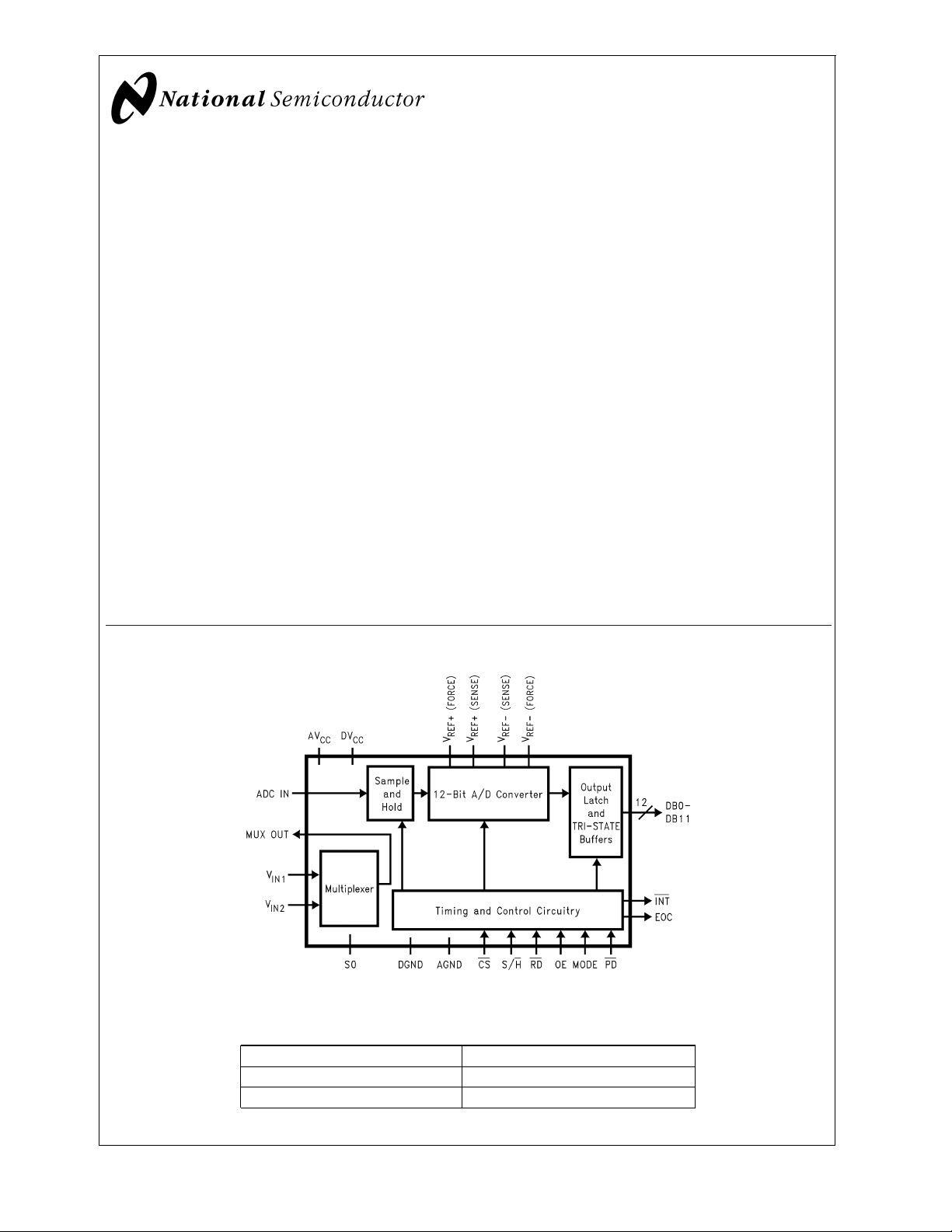
Using an innovative multistep conversion technique, the
12-bit ADC12662 CMOS analog-to-digital converter digitizes
signals at a 1.5 MHz sampling rate while consuming a maximum of only 200 mW on a single +5V supply. The
ADC12662 performs a 12-bit conversion in three
lower-resolution “flash” conversions, yielding a fast A/D without the cost and power dissipation associated with true flash
approaches.
The analog input voltage to the ADC12662 is tracked and
held by an internal sampling circuit, allowing high frequency
input signals to be accurately digitized without the need for
an external sample-and-hold circuit. The ADC12662 features
two sample-and-hold/flash comparator sections which allow
the converter to acquire one sample while converting the
previous. This pipelining technique increases conversion
speed without sacrificing performance. The multiplexer output is available to the user in order to perform additional
external signal processing before the signal is digitized.
When the converter is not digitizing signals, it can be placed
in the Standby mode; typical power consumption in this
mode is 250 µW.
ADC12662 Block Diagram
Features
n Built-in sample-and-hold
n Single +5V supply
n Single channel or 2 channel multiplexer operation
n Low Power Standby mode
Key Specifications
n Sampling rate 1.5 MHz (min)
n Conversion time 580 ns (typ)
n Signal-to-Noise Ratio, f
n Power consumption (f
n No missing codes over temperature Guaranteed
= 100 kHz 67.5 dB (min)
IN
= 1.5 MHz) 200 mW (max)
s
Applications
n Digital signal processor front ends
n Instrumentation
n Disk drives
n Mobile telecommunications
n Waveform digitizers
01187601
Ordering Information
Industrial (−40˚C ≤ TA≤ +85˚) Package
ADC12662CIV V44 Plastic Leaded Chip Carrier
ADC12662CIVF VGZ44A Plastic Quad Flat Package
© 2001 National Semiconductor Corporation DS011876 www.national.com
Page 2
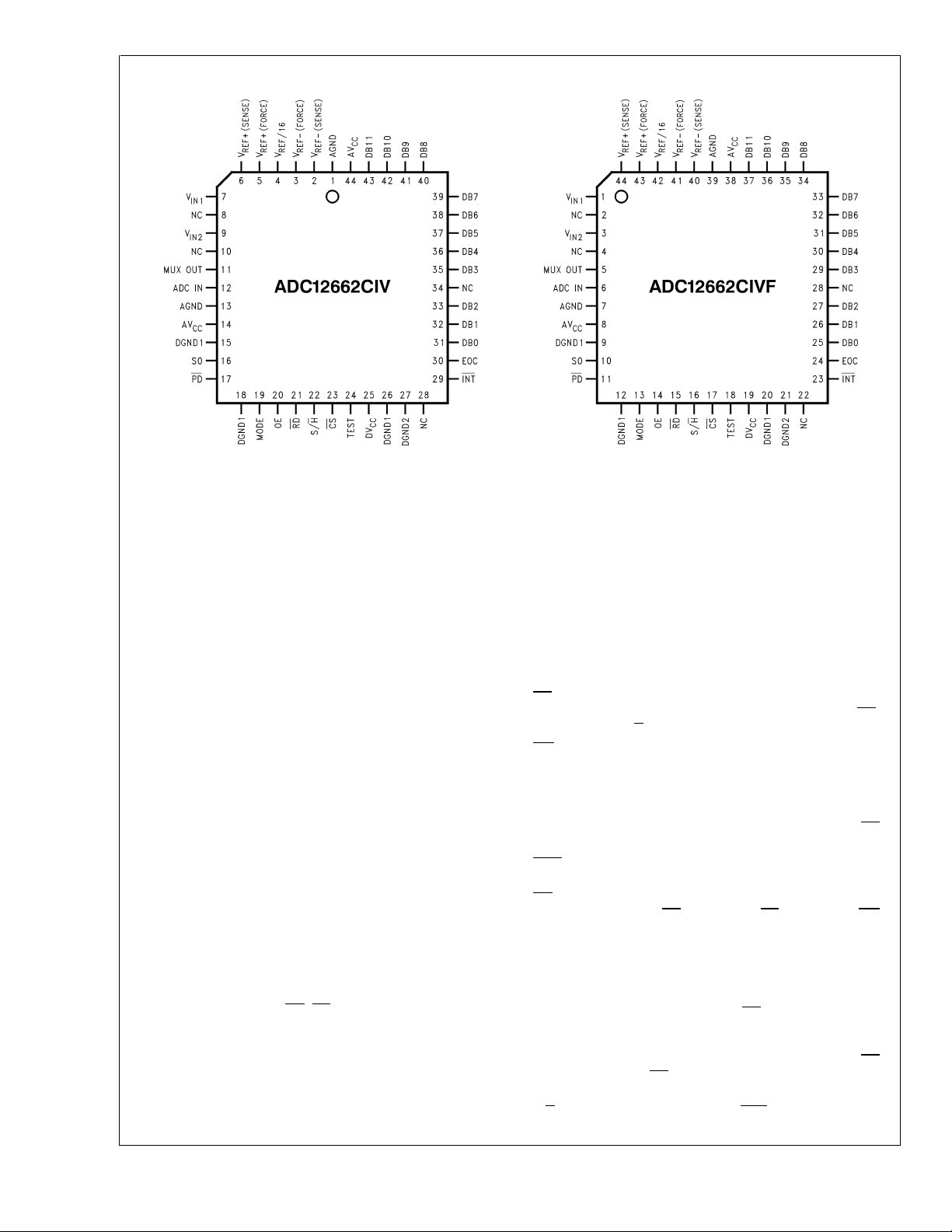
Connection Diagrams
ADC12662
Top View
01187615
Pin Descriptions
AV
CC
DV
CC
AGND, DGND1,
DB0–DB11 These are the TRI-STATE output pins, en-
V
IN1,VIN2
MUX OUT This is the output of the on-board analog
These are the two positive analog supply
inputs. They should always be connected to
the same voltage source, but are brought out
separately to allow for separate bypass capacitors. Each supply pin should be bypassed to AGND with a 0.1 µF ceramic capacitor in parallel with a 10 µF tantalum
capacitor.
This is the positive digital supply input. It
should always be connected to the same
voltage as the analog supply, AV
. It should
CC
be bypassed to DGND2 with a 0.1 µF ceramic capacitor in parallel with a 10 µF tantalum capacitor.
DGND2
These are the power supply ground pins.
There are separate analog and digital ground
pins for separate bypassing of the analog
and digital supplies. The ground pins should
be connected to a stable, noise-free system
ground. All of the ground pins should be
returned to the same potential. AGND is the
analog ground for the converter. DGND1 is
the ground pin for the digital control lines.
DGND2 is the ground return for the output
databus. See Section 6.0 LAYOUT AND
GROUNDING for more information.
abled by RD, CS, and OE.
These are the analog input pins to the multi-
plexer. For accurate conversions, no input
pin (even one that is not selected) should be
driven more than 50 mV below ground or 50
mV above V
.
CC
input multiplexer.
Top View
01187629
ADC IN This is the direct input to the 12-bit sampling
A/D converter. For accurate conversions,
this pin should not be driven more than 50
mV below ground or 50 mV above V
.
CC
S0 This pin selects the analog input that will be
connected to the ADC12662 during the conversion. The input is selected based on the
state of S0 when EOC makes its high-to-low
transition. Low selects V
V
.
IN2
, high selects
IN1
MODE This pin should be tied to DGND1.
CS
This is the active low Chip Select control
input. When low, this pin enables the RD,
S/H, and OE inputs. This pin can be tied low.
INT This is the active low Interrupt output. When
using the Interrupt Interface Mode (
Figure 1
this output goes low when a conversion has
been completed and indicates that the conversion result is available in the output
latches. This output is always high when RD
EOC
is held low (
This is the End-of-Conversion control output.
Figure 2
).
This output is low during a conversion.
RD
This is the active low Read control input.
When RD is low (and CS is low), the INT
output is reset and (if OE is high) data appears on the data bus. This pin can be tied
low.
OE This is the active high Output Enable control
input. This pin can be thought of as an inverted version of the RD input (see
Figure 6
Data output pins DB0–DB11 are TRI-STATE
when OE is low. Data appears on
DB0–DB11 only when OE is high and CS
and RD are both low. This pin can be tied
high.
S/H
This is the Sample/Hold control input. The
analog input signal is held and a new conver-
),
).
www.national.com 2
Page 3

Pin Descriptions (Continued)
sion is initiated by the falling edge of this
control input (when CS is low).
PD This is the Power Down control input. This
pin should be held high for normal operation.
When this pin is pulled low, the device goes
into a low power standby mode.
V
REF+(FORCE)
,V
REF−(FORCE)
These are the positive and negative voltage
reference force inputs, respectively. See
Section 4, REFERENCE INPUTS, for more
information.
V
REF+(SENSE)
,V
REF−(SENSE)
These are the positive and negative voltage
reference sense pins, respectively. See Section 4, REFERENCE INPUTS, for more
information.
V
/16 This pin should be bypassed to AGND with a
REF
0.1 µF ceramic capacitor.
TEST This pin should be tied to DV
.
CC
ADC12662
www.national.com3
Page 4
Absolute Maximum Ratings (Notes 1,
2)
If Military/Aerospace specified devices are required,
ADC12662
please contact the National Semiconductor Sales Office/
Distributors for availability and specifications.
Supply Voltage (V
) −0.3V to +6V
AV
CC
Voltage at Any Input or Output −0.3V to V
=DVCC=
CC
+
CC
VF Package
Vapor Phase (60 seconds) 215˚C
Infrared (15 seconds) 220˚C
Storage Temperature Range −65˚C to +150˚C
Maximum Junction Temperature
(T
) 150˚C
JMAX
Operating Ratings (Notes 1, 2)
0.3V
Input Current at Any Pin (Note 3) 25 mA
Package Input Current (Note 3) 50 mA
Power Dissipation (Note 4)
ADC12662CIV 875 mW
ESD Susceptibility (Note 5) 2000V
Temperature Range T
ADC12662CIV, ADC12662CIVF −40˚C ≤ TA≤
Supply Voltage Range
=AVCC) 4.75V to 5.25V
(DV
CC
MIN
Soldering Information (Note 6)
V Package, Infrared, 15 seconds +300˚C
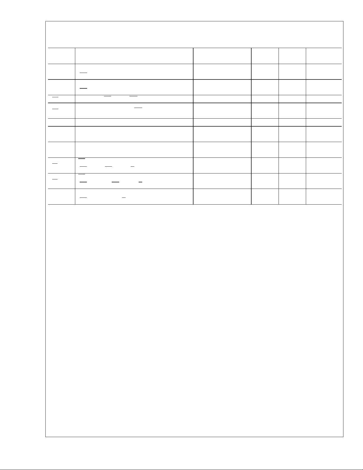
Converter Characteristics
The following specifications apply for DVCC=AVCC= +5V, V
unless otherwise specified. Boldface limits apply for T
A=TJ
REF+(SENSE)
from T
Symbol Parameter Conditions Typ Limit Units
Resolution 12 Bits
R
V
V
V
C
C
REF
REF(+)
REF(−)
IN
ADC
MUX
Differential Linearity Error T
Integral Linearity Error
(Note 9)
Offset Error T
Full-Scale Error T
Power Supply Sensitivity
(Note 15)
Reference Resistance 1000
V
REF+(SENSE)
V
REF−(SENSE)
Input Voltage AV
Input Voltage AGND V (min)
Input Voltage Range To V
ADC IN Input Leakage AGND to AV
ADC IN Input Capacitance 25 pF
MUX On-Channel Leakage AGND to AV
MUX Off-Channel Leakage AGND to AV
Multiplexer Input Cap 7 pF
MUX Off Isolation f
to T
T
DV
IN
MIN
MIN
MIN
MIN
MAX
to T
MAX
to T
MAX
to T
MAX
=AVCC=5V±5%
CC
IN1,VIN2
, or ADC IN
− 0.3V 0.1 3 µA (max)
CC
− 0.3V 0.1 3 µA (max)
CC
− 0.3V 0.1 3 µA (max)
CC
= 100 kHz 92 dB
= +4.096V, V
to T
MIN
REF−(SENSE)
; all other limits TA=TJ= +25˚C.
MAX
= AGND, and fs= 1.5 MHz,
(Note 7) (Note 8) (Limit)
±
0.4
±
0.4
±
0.3
±
0.3
±
0.95 LSB (max)
±
1.5 LSB (max)
±
2.0 LSB (max)
±
1.5 LSB (max)
±
0.75 LSB (max)
600 Ω (min)
1300 Ω (max)
CC
AV
+0.05V V (max)
CC
AGND − 0.05V V (min)
≤ TA≤ T
+85˚C
V (max)
MAX
Dynamic Characteristics (Note 10)
The following specifications apply for DVCC=AVCC= +5V, V
100 kHz, 0 dB from fullscale, and f
T
; all other limits TA=TJ= +25˚C.
MAX
= 1.5 MHz, unless otherwise specified. Boldface limits apply for TA=TJfrom T
s
REF+(SENSE)
Symbol Parameter Conditions Typ Limit Units
SINAD Signal-to-Noise Plus
Distortion Ratio
www.national.com 4
T
to T
MIN
MAX
= +4.096V, V
(Note 7) (Note 8) (Limit)
REF−(SENSE)
= AGND, RS=25Ω,fIN=
70 67.0 dB (min)
MIN
to
Page 5
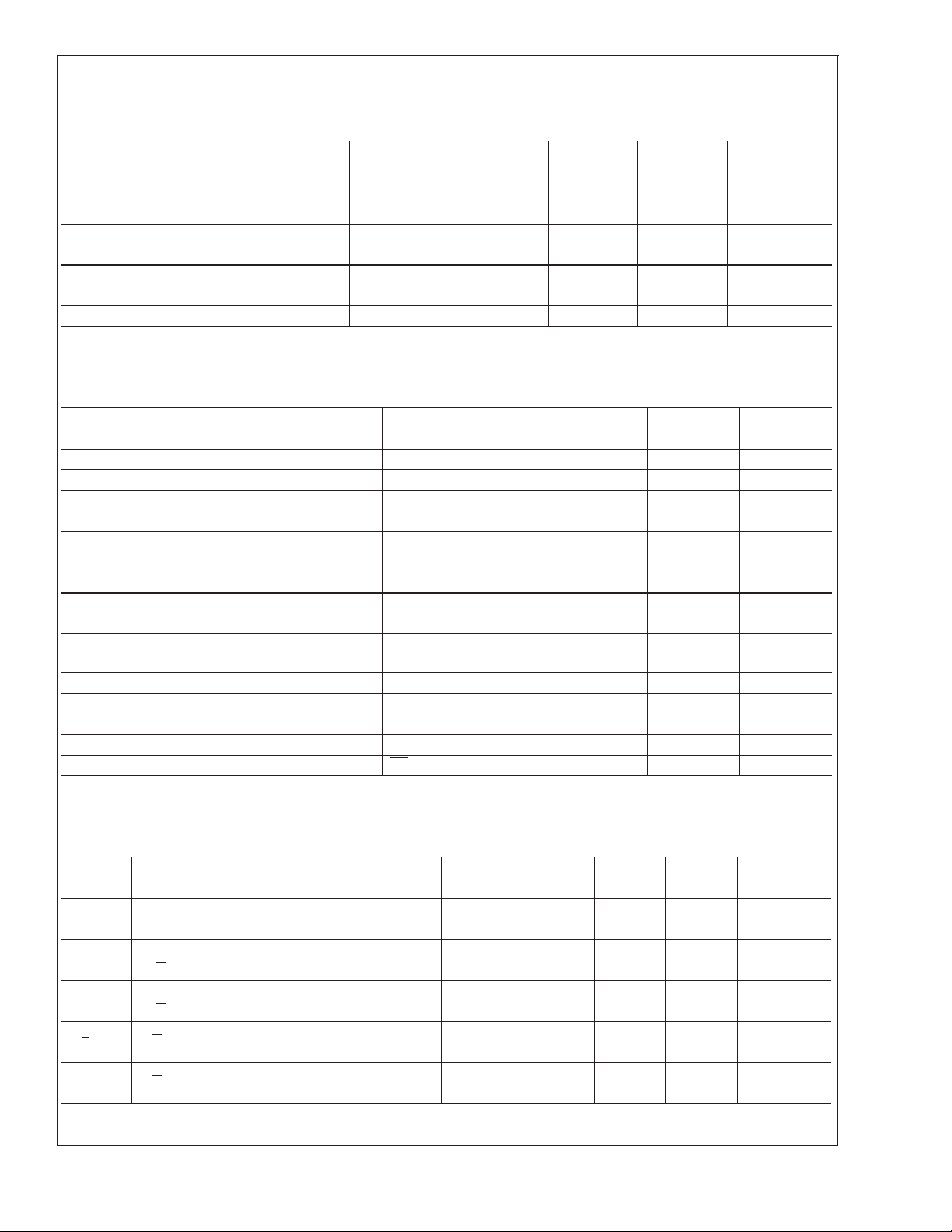
Dynamic Characteristics (Note 10) (Continued)
The following specifications apply for DVCC=AVCC= +5V, V
100 kHz, 0 dB from fullscale, and f
T
; all other limits TA=TJ= +25˚C.
MAX
= 1.5 MHz, unless otherwise specified. Boldface limits apply for TA=TJfrom T
s
REF+(SENSE)
Symbol Parameter Conditions Typ Limit Units
SNR Signal-to-Noise Ratio
(Note 11)
THD Total Harmonic Distortion
(Note 12)
ENOB Effective Number of Bits
(Note 13)
IMD Intermodulation Distortion f
T
to T
MIN
T
MIN
T
MIN
IN
MAX
to T
MAX
to t
MAX
= 88.7 kHz, 89.5 kHz −80 dBc
= +4.096V, V
(Note 7) (Note 8) (Limit)
REF−(SENSE)
= AGND, RS=25Ω,fIN=
70 67.5 dB (min)
−80 −70 dBc (max)
11.3 10.8 Bits (min)
DC Electrical Characteristics
The following specifications apply for DVCC=AVCC= +5V, V
unless otherwise specified. Boldface limits apply for T
A=TJ
REF+(SENSE)
from T
Symbol Parameter Conditions Typ Limit Units
V
IN(1)
V
IN(0)
I
IN(1)
I
IN(0)
V
OUT(1)
V
OUT(0)
I
OUT
C
OUT
C
IN
DI
CC
AI
CC
I
STANDBY
Logical “1” Input Voltage DVCC=AVCC= +5.5V 2.0 V (min)
Logical “0” Input Voltage DVCC=AVCC= +4.5V 0.8 V (max)
Logical “1” Input Current 0.1 1.0 µA (max)
Logical “0” Input Current 0.1 1.0 µA (max)
=AVCC= +4.5V,
DV
CC
Logical “1” Output Voltage
Logical “0” Output Voltage
TRI-STATE®Output
Leakage Current
I
= −360 µA 2.4 V (min)
OUT
I
= −100 µA 4.25 V (min)
OUT
DV
=AVCC= +4.5V,
CC
= 1.6 mA
I
OUT
Pins DB0–DB11 0.1 3 µA (max)
TRI-STATE Output Capacitance Pins DB0–DB11 5 pF
Digital Input Capacitance 4 pF
DVCCSupply Current 2 3 mA (max)
AVCCSupply Current 32 37 mA (max)
Standby Current (DICC+AICC) PD=0V 50 µA
= +4.096V, V
to T
MIN
REF−(SENSE)
; all other limits TA=TJ= +25˚C.
MAX
= AGND, and fs= 1.5 MHz,
(Note 7) (Note 8) (Limit)
0.4 V (max)
MIN
ADC12662
to
AC Electrical Characteristics
The following specifications apply for DVCC=AVCC= +5V, V
unless otherwise specified. Boldface limits apply for T
A=TJ
REF+(SENSE)
from T
Symbol Parameter Conditions Typ Limit Units
f
s
t
CONV
t
AD
t
S/H
t
EOC
Maximum Sampling Rate
(1/t
THROUGHPUT
)
Conversion Time
(S/H Low to EOC High)
Aperture Delay
(S/H Low to Input Voltage Held)
S/H Pulse Width 10
S/H Low to EOC Low 90
= +4.096V, V
to T
MIN
REF−(SENSE)
; all other limits TA=TJ= +25˚C.
MAX
= AGND, and fs= 1.5 MHz,
(Note 7) (Note 8) (Limits)
1.5 MHz (min)
580
510 ns (min)
660 ns (max)
20 ns
400 ns (max)
60 ns (min)
126 ns (max)
5 ns (min)
www.national.com5
Page 6
AC Electrical Characteristics (Continued)
The following specifications apply for DVCC=AVCC= +5V, V
unless otherwise specified. Boldface limits apply for T
ADC12662
Symbol Parameter Conditions Typ Limit Units
t
ACC
t1H,t
t
INTH
t
INTL
t
UPDATE
t
MS
t
MH
t
CSS
t
CSH
t
WU
Note 1: Absolute Maximum Ratings indicate limits beyond which damage to the device may occur. Operating Ratings indicate conditions for which the device is
functional. These ratings do not guarantee specific performance limits, however.For guaranteed specifications and test conditions, see the Electrical Characteristics.
The guaranteed specifications apply only for the test conditions listed. Some performance characteristics may degrade when the device is not operated under the
listed test conditions.
Note 2: All voltages are measured with respect to GND (GND = AGND = DGND), unless otherwise specified.
Note 3: When the input voltage (V
to 25 mA or less. The 50 mA package input current limits the number of pins that can safely exceed the power supplies with an input current of 25 mA to two.
Note 4: The maximum power dissipation must be derated at elevated temperatures and is dictated by T
allowable power dissipation at any temperature is P
(PLCC) package is 55˚C/W. θ
conditions.
Note 5: Human body model, 100 pF discharged through a 1.5 kΩ resistor. Machine model ESD rating is 200V.
Note 6: See AN-450 “Surface Mounting Methods and Their Effect on Product Reliability” or the section titled “Surface Mount” found in a current National
Semiconductor Linear Data Book for other methods of soldering surface mount devices.
Note 7: Typicals are at +25˚C and represent most likely parametric norm.
Note 8: Tested limits are guaranteed to National’s AOQL (Average Outgoing Quality Level).
Note 9: Integral Linearity Error is the maximum deviation from a straight line between the
Note 10: Dynamic testing of the ADC12662 is done using the ADC IN input. The input multiplexer adds harmonic distortion at high frequencies. See the graph in
the Typical Performance Characteristics section for a typical graph of THD performance vs input frequency with and without the input multiplexer.
Note 11: The signal-to-noise ratio is the ratio of the signal amplitude to the background noise level. Harmonics of the input signal are not included in its calculation.
Note 12: The contributions from the first nine harmonics are used in the calculation of the THD.
Note 13: Effective Number of Bits (ENOB) is calculated from the measured signal-to-noise plus distortion ratio (SINAD) using the equation ENOB = (SINAD −
1.76)/6.02.
Note 14: The digital power supply current takes up to 10 seconds to decay to its final value after PD is pulled low. This prohibits production testing of the standby
current. Some parts may exhibit significantly higher standby currents than the 50 µA typical.
Note 15: Power Supply Sensitivity is defined as the change in the Offset Error or the Full Scale Error due to a change in the supply voltage.
Access Time
(RD Low or OE High to Data Valid)
TRI-STATE Control
0H
(RD High or OE Low to Databus TRI-STATE)
Delay from RD Low to INT High CL= 100 pF 35 60 ns (max)
Delay from EOC High to INT Low CL= 100 pF −25
EOC High to New Data Valid 5 15 ns (max)
Multiplexer Address Setup Time
(MUX Address Valid to EOC Low)
Multiplexer Address Hold Time
(EOC Low to MUX Address Invalid)
CS Setup Time
(CS Low to RD Low, S/H Low, or OE High)
CS Hold Time
(CS High after RD High, S/H High, or OE Low)
Wake-Up Time
(PD High to First S/H Low)
) at any pin exceeds the power supply rails (V
IN
=(T
for the VF (PQFP) package is 62˚C/W. In most cases the maximum derated power dissipation will be reached only during fault
JA
D
)/θJAor the number given in the Absolute Maximum Ratings, whichever is lower. θJAfor the V
JMAX−TA
A=TJ
REF+(SENSE)
from T
C
L
R
L
<
IN
= +4.096V, V
to T
MIN
REF−(SENSE)
; all other limits TA=TJ= +25˚C.
MAX
= AGND, and fs= 1.5 MHz,
(Note 7) (Note 8) (Limits)
= 100 pF 10 20 ns (max)
= 1k, CL=10pF 25 40 ns (max)
−35 ns (min)
−5 ns (max)
50 ns (min)
50 ns (min)
20 ns (min)
20 ns (min)
1µs
GND or V
>
VCC) the absolute value of current at that pin should be limited
IN
, θJAand the ambient temperature TA. The maximum
JMAX
measured
offset and full scale endpoints.
www.national.com 6
Page 7
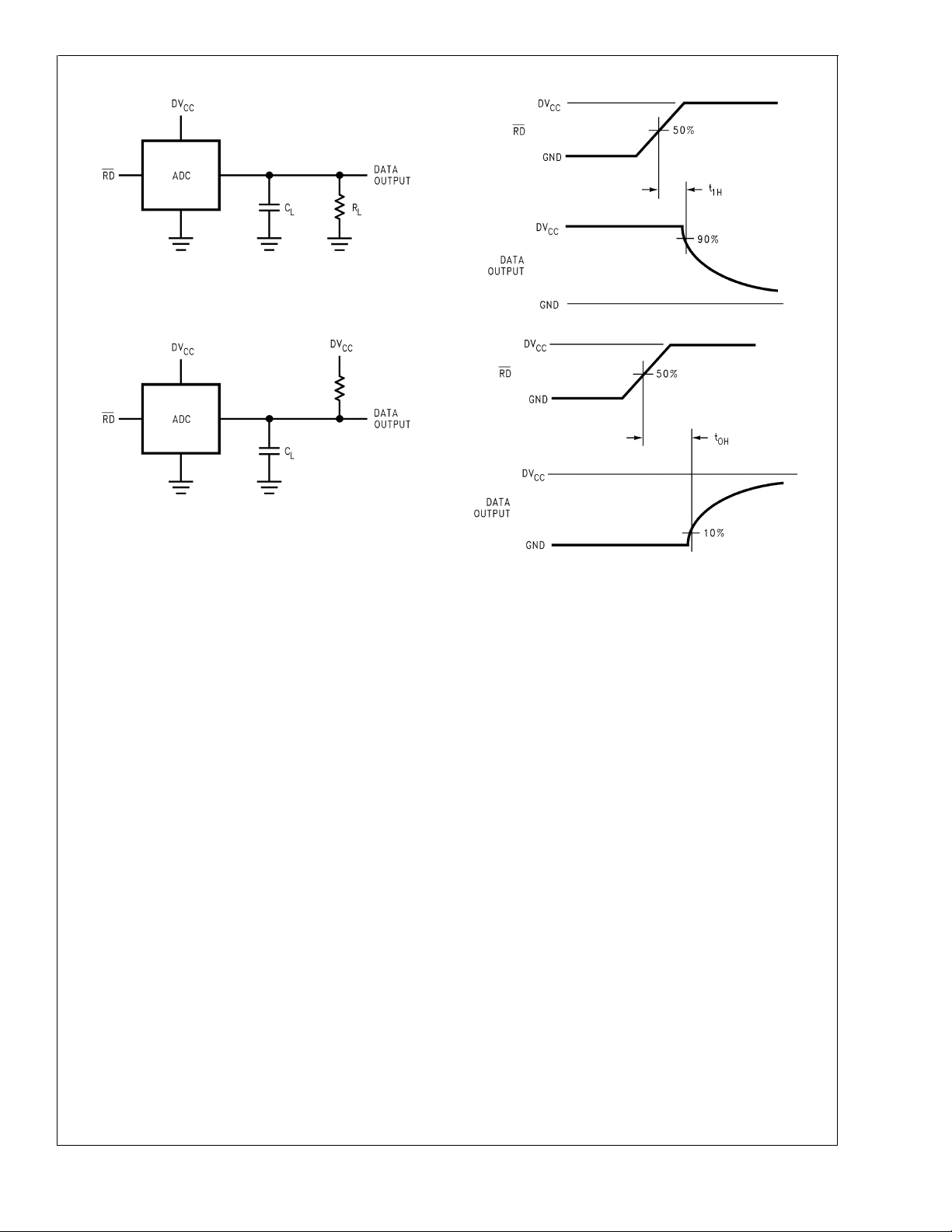
TRI-STATE Test Circuit and Waveforms
01187602
ADC12662
01187603
01187604
01187605
www.national.com7
Page 8

Typical Performance Characteristics
Offset and Fullscale
ADC12662
Error Change vs
Reference Voltage
Linearity Error Change
vs Reference Voltage
Mux ON Resistance
vs Input Voltage
Digital Supply Current
vs Temperature
Conversion Time (t
CONV
vs Temperature
01187630
01187633
)
01187631
Current Consumption in
Analog Supply Current
vs Temperature
EOC Delay Time (t
EOC
01187634 01187635
)
Standby Mode vs Voltage
on Digital Input Pins
vs Temperature Spectral Response
01187632
01187636
www.national.com 8
01187637
01187638
Page 9

Typical Performance Characteristics (Continued)
ADC12662
SINAD vs Input Frequency
(ADC In)
01187639 01187640
SINAD vs Input Frequency
(Through Mux)
SNR vs Input Frequency
(ADC In)
SNR vs Input Frequency
(Through Mux)
THD vs Input Frequency
(ADC In)
01187641
THD vs Input Frequency
(Through Mux)
SNR and THD vs Source
Impedance
01187642 01187643 01187644
SNR and THD vs
Reference Voltage
01187645
01187646
www.national.com9
Page 10

Timing Diagrams
ADC12662
01187609
FIGURE 1. Interrupt Interface Timing (MODE = 0, OE = 1)
FIGURE 2. High Speed Interface Timing (MODE = 0, OE = 1, CS = 0, RD = 0)
01187610
www.national.com 10
Page 11

Timing Diagrams (Continued)
FIGURE 3. CS Setup and Hold Timing for S/H, RD, and OE
ADC12662
01187613
www.national.com11
Page 12

Functional Description
The ADC12662 performs a 12-bit analog-to-digital conversion using a 3 step flash technique. The first flash deter-
ADC12662
mines the six most significant bits, the second flash generates four more bits, and the final flash resolves the two least
significant bits.
the converter. It consists of a 2
resistor ladder with two different resolution voltage spans, a
Figure 4
shows the major functional blocks of
1
⁄2-bit Voltage Estimator, a
sample/hoId capacitor, a 4-bit flash converter with front end
multiplexer, a digitally corrected DAC, and a capacitive voltage divider. To pipeline the converter, there are two sample/
hold capacitors and 4-bit flash sections, which allows the
converter to acquire the next input sample while converting
the previous one. Only one of the flash converter pairs is
shown in
Figure 4
to reduce complexity.
FIGURE 4. Functional Block Diagram
The resistor string near the center of the block diagram in
Figure 4
generates the 6-bit and 10-bitreference voltages for
the first two conversions. Each of the 16 resistors at the
bottom of the string is equal to 1/1024 of the total string
resistance. These resistors form the LSB Ladder (The
weight of each resistor on the LSB ladder is actually equivalent to four 12-bit LSBs. It is called the LSB ladder because
it has the highest resolution of all the ladders in the converter) and have a voltage drop of 1/1024 of the total reference voltage (V
REF+
−V
) across each of them. The
REF−
remaining resistors form the MSB Ladder. It is comprised of
eight groups of eight resistors each connected in series (the
lowest MSB ladder resistor is actually the entire LSB ladder).
Each MSB Ladder section has
1
⁄8of the total reference
voltage across it. Within a given MSB ladder section, each of
the eight MSB resistors has 1/64 of the total reference
voltage across it. Tap points are found between all of the
www.national.com 12
01187616
resistors in both the MSB and LSB ladders. The Comparator
MultipIexer can connect any of these tap points, in two
adjacent groups of eight, to the sixteen comparators shown
at the right of
Figure 4
. This function provides the necessary
reference voltages to the comparators during the first two
flash conversions.
The six comparators, seven-resistor string (Estimator DAC
ladder), and Estimator Decoder at the left of
Figure 4
form
the Voltage Estimator. The Estimator DAC, connected between V
REF+
and V
, generates the reference voltages
REF−
for the six Voltage Estimator comparators. The comparators
perform a very low resoIution A/D conversion to obtain an
“estimate” of the input voltage. This estimate is used to
control the placement of the Comparator Multiplexer, connecting the appropriate MSB ladder section to the sixteen
flash comparators. A total of only 22 comparators (6 in the
Page 13

Functional Description (Continued)
Voltage Estimator and 16 in the flash converter) is required
to quantize the input to 6 bits, instead of the 64 that would be
required using a traditional 6-bit flash.
Prior to a conversion, the Sample/Hold switch is closed,
allowing the voltage on the S/H capacitor to track the input
voItage. Switch 1 is in position 1. A conversion begins by
opening the Sample/Hold switch and latching the output of
the Voltage Estimator. The estimator decoder then selects
two adjacent banks of tap points aIong the MSB ladder.
These sixteen tap points are then connected to the sixteen
flash converters. For exampIe, ifthe input voltage is between
5/16 and 7/16 of V
REF(VREF=VREF+−VREF−
decoder instructs the comparator multiplexer to select the
sixteen tap points between 2/8 and 4/8 (4/16 and 8/16) of
V
and connects them to the sixteen flash converters. The
REF
first flash conversion is now performed, producing the first 6
MSBs of data.
At this point, Voltage Estimator errors as large as 1/16 of
V
will be corrected since the flash converters are con-
REF
nected to ladder voltages that extend beyond the range
specified by the Voltage Estimator. For example, if
<
(7/16)V
REF
<
V
(9/16)V
IN
, the Voltage Estimator’s
REF
comparators tied to the tap points below (9/16)V
output “1”s (000111). This is decoded by the estimator decoder to “10”. The 16 comparators will be placed on the MSB
ladder tap points between (
lap of (1/16)V
will automatically cancel a Voltage Estima-
REF
3
⁄8)V
REF
and (5⁄8)V
tor error of up to 256 LSBs. If the first flash conversion
determines that the input voltage is between (
((4/8)V
− LSB/2), the VoltageEstimator’s output code will
REF
be corrected by subtracting “1”, resulting in a corrected value
of “01” for the first two MSBs. If the first flash conversion
determines that the input voltage is between (4/8)V
LSB/2) and (
5
⁄8)V
, the voltage estimator’s output code is
REF
unchanged.
The results of the first flash and the Voltage Estimator’s
output are given to the factory-programmed on-chip EEPROM which returns a correction code corresponding to the
error of the MSB ladder at that tap. This code is converted to
a voltage by the Correction DAC. To generate the next four
bits, SW1 is moved to position 2, so the ladder voltage and
the correction voltage are subtracted from the input voltage.
The remainder is applied to the sixteen flash converters and
compared with the 16 tap points from the LSB ladder.
), the estimator
will
REF
. This over-
REF
3
⁄8)V
REF
and
REF
ADC12662
The result of this second conversion is accurate to 10 bits
and describes the input remainder as a voltage between two
tap points (V
two bits, the voltage across the ladder resistor (between V
and VL) on the LSB ladder.To resolve the last
H
H
and VL) is divided up into 4 equal parts by the capacitive
voltage divider, shown in
LSBs below V
and 6 LSBs above VHto provide overlap
L
Figure 5
. The divider also creates 6
used by the digital error correction. SW1 is moved to position
3, and the remainder is compared with these 16 new voltages. The output is combined with the results of the Voltage
Estimator,first flash, and second flash to yield the final 12-bit
result.
By using the same sixteen comparators for all three flash
conversions, the number of comparators needed by the
multi-step converter is significantly reduced when compared
to standard multi-step techniques.
Applications Information
1.0 MODES OF OPERATION
The ADC12662 has two interface modes: An interrupt/read
mode and a high speed mode.
timing diagrams for these interfaces.
In order to clearly show the relationship between S/H, CS,
RD, and OE, the control logic decoding section of the
ADC12662 is shown in
Figure 6
Interrupt Interface
As shown in
Figure 1
, the falling edge of S/H holds the input
voltage and initiates a conversion. At the end of the conversion, the EOC output goes high and the INT output goes low,
indicating that the conversion results are latched and may be
read by pulling RD low.The falling edge of RD resets the INT
−
line. Note that CS must be low to enable S/H or RD.
High Speed Interface
The Interrupt interface works well at lower speeds, but few
microprocessors could keep up with the 1 µs interrupts that
would be generated if the ADC12662 was running at full
speed. The most efficient interface is shown in
Here the output data is always present on the databus, and
the INT to RD delay is eliminated.
Figure 1
.
and2show the
Figure 2
.
www.national.com13
Page 14

Applications Information (Continued)
ADC12662
FIGURE 5. The Capacitive Voltage Divider
01187617
FIGURE 6. ADC Control Logic
2.0 THE ANALOG INPUT
The analog input of the ADC12662 can be modeled as two
small resistances in series with the capacitance of the input
hold capacitor (C
), as shown in
IN
Figure 7
. The S/H switch is
closed during the Sample period, and open during Hold. The
source has to charge C
to the input voltage within the
IN
sample period. Note that the source impedance of the input
voltage (R
charge C
IN
will not settle to within 0.5 LSBs of V
) has a direct effect on the time it takes to
SOURCE
.IfR
SOURCE
is too large, the voltage across C
SOURCE
before the
IN
conversion begins, and the conversion results will be incorrect. From a dynamic performance viewpoint, the combination of R
SOURCE,RMUX,RSW
Minimizing R
SOURCE
, and CINform a low pass filter.
will increase the frequency response of
the input stage of the converter.
Typical values for the components shown in
R
= 100Ω,RSW= 100Ω, and CIN= 25 pF. The settling
MUX
Figure 7
are:
time to n bits is:
t
SETTLE
=(R
SOURCE
+R
MUX+RSW
)*C
IN
*n*
ln (2).
The bandwidth of the input circuit is:
www.national.com 14
01187618
= 1/(2*3.14*(R
f
−3dB
SOURCE
+R
MUX+RSW
)*CIN)
The ADC12662 is operated in a pipelined sequence, with
one hold capacitor acquiring the next sample while a conversion is being performed on the voltage stored on the other
hold capacitor. This gives the source over t
CONV
seconds to
charge the hold capacitor to its final value. At 1.5 MHz, the
settling time must be less than 667 ns. Using the settling
time equation and component values given, the maximum
source impedance that will allow the input to settle to
(n = 13) at full speed is ∼2.8 kΩ. To ensure
1
over temperature and device-to-device variation, R
1
⁄2LSB
⁄2LSB settling
SOURCE
should be a maximum of 500Ω when the converter is operated at full speed.
If the signal source has a high output impedance, its output
should be buffered with an operational amplifier capable of
driving a switched 25 pF/100Ω load. Any ringing or instabilities at the op amp’s output during the sampling period can
result in conversion errors. The LM6361 high speed op amp
is a good choice for this application due to its speed and its
ability to drive large capacitive loads.
Figure 8
shows the
Page 15

Applications Information (Continued)
LM6361 driving the ADC IN input of an ADC12662. The
100 pF capacitor at the input of the converter absorbs some
of the high frequency transients generated by the S/H
switching, reducing the op amp transient response requirements. The 100 pF capacitor should only be used with high
speed op amps that are unconditionally stable driving capacitive loads.
Another benefit of using a high speed buffer is improved
THD performance when using the multiplexer of the
ADC12662. The MUX on-resistance is somewhat non-linear
over input voltage, causing the RC time constant formed by
C
IN,RMUX
, and RSWto vary depending on the input voltage.
This results in increasing THD with increasing frequency.
Inserting the buffer between the MUX OUT and the ADC IN
terminals as shown in
R
, significantly reducing the THD of the multiplexed
MUX
Figure 8
will eliminate the loading on
system.
ADC12662
FIGURE 7. Simplified ADC12662 Input Stage
FIGURE 8. Buffering the Input with an LM6361 High Speed Op Amp
Correct converter operation will be obtained for input voltages greater than AGND − 50 mV and less than AV
+50
CC
mV. Avoid driving the signal source more than 300 mV
higher than AV
, or more than 300 mV below AGND. If an
CC
analog input pin is forced beyond these voltages, the current
flowing through that pin should be limited to 25 mA or less to
avoid permanent damage to the IC. The sum of all the
01187619
01187620
overdrive currents into all pins must be less than 50 mA.
When the input signal is expected to extend more than
300 mV beyond the power supply limits for any reason
(unknown/uncontrollable input voltage range, power-on transients, fault conditions, etc.) some form of input protection,
such as that shown in
Figure 9
, should be used.
www.national.com15
Page 16

Applications Information (Continued)
ADC12662
FIGURE 9. Input Protection
3.0 ANALOG MULTIPLEXER
The ADC12662 has an input multiplexer that is controlled by
the logic level on pin S0 when EOC goes low, as shown in
Figure 1
and2.Multiplexer setup and hold times with respect
to the S/H input can be determined by these two equations:
t
MS (wrt S/H)=tMS−tEOC (min)
t
MH (wrt S/H)=tMH+tEOC (max)
Note that t
MS (wrt S/H)
is a negative number; this indicates that
= 50 − 60 = −10 ns
= 50 + 125 = 175 ns
the data on S0 must become valid within 10 ns after S/H
goes low in order to meet the setup time requirements. S0
must be valid for a length of
Table 1
(t
MH+tEOC (max)
shows how the input channels are assigned:
)−(tMS−t
EOC (min)
) = 185 ns.
TABLE 1. ADC12662 Input
Multiplexer Programming
S0 Channel
0V
1V
IN1
IN2
The output of the multiplexer is available to the user via the
MUX OUT pin. This output allows the user to perform additional signal processing, such as filtering or gain, before the
01187621
signal is returned to the ADC IN input and digitized. If no
additional signal processing is required, the MUX OUT pin
should be tied directly to the ADC IN pin.
See Section 9.0 (APPLICATIONS) for a simple circuit that
will alternate between the two inputs while converting at full
speed.
4.0 REFERENCE INPUTS
In addition to the fully differential V
REF+
and V
REF−
reference
inputs used on most National Semiconductor ADCs, the
ADC12662 has two sense outputs for precision control of the
ladder voltage. These sense inputs compensate for errors
due to IR drops between the reference source and the ladder
itself. The resistance of the reference ladder is typically
750Ω. The parasitic resistance (R
) of the package leads,
P
bond wires, PCB traces, etc. can easily be 0.5Ω to 1.0Ω or
more. This may not be significant at 8-bit or 10-bit resolutions, but at 12 bits it can introduce voltage drops causing
offset and gain errors as large as 6 LSBs.
The ADC12662 provides a means to eliminate this error by
bringing out two additional pins that sense the exact voltage
at the top and bottom of the ladder. With the addition of two
op amps, the voltages on these internal nodes can be forced
to the exact value desired, as shown in
Figure 10
.
www.national.com 16
Page 17

Applications Information (Continued)
ADC12662
FIGURE 10. Reference Ladder Force and Sense Inputs
Since the current flowing through the SENSE lines is essentially zero, there is negligible voltage drop across R
and the
S
1kΩresistor, so the voltage at the inverting input of the op
amp accurately represents the voltage at the top (or bottom)
of the ladder. The op amp drives the FORCE input and
forces the voltage at the ends of the ladder to equal the
voltage at the op amps’s non-inverting input, plus or minus
its input offset voltage. For this reason op amps with low
V
, such as the LM627 or LM607, should be used for this
OS
application. When used in this configuration, the ADC12662
has less than 2 LSBs of offset and 1.5 LSB of gain error
without any user adjustments.
The 0.1 µF and 10 µF capacitors on the force inputs provide
high frequency decoupling of the reference ladder.The 500Ω
force resistors isolate the op amps from this large capacitive
load. The 0.01 µF/1 kΩ network provides zero phase shift at
high frequencies to ensure stability. Note that the op amp
supplies in this example must be
±
10V to±15V to meet the
input/output voltage range requirements of the LM627 and
supply the sub-zero voltage to the V
V
output should be bypassed to analog ground with a
REF/16
REF− (FORCE)
pin. The
0.1 µF ceramic capacitor.
The reference inputs are fully differential and define the zero
to full-scale range of theinput signal.They can be configured
01187622
to span up to 5V (V
REF−
=0V,V
= 5V), or they can be
REF+
connected to different voltages (within the 0V to 5V limits)
when other input spans are required. The ADC12662 is
tested at V
REF− (SENSE)
=0V,V
REF+ (SENSE)
= 4.096V. Reducing the reference voltage span to less than 4V increases
the sensitivity (reduces the LSB size) of the converter; however noise performance degrades when lower reference
voltages are used. A plot of dynamic performance vs reference voltage is given in the Typical Performance Characteristics section.
If the converter will be used in an application where DC
accuracy is secondary to dynamic performance, then a simpler reference circuit may suffice. The circuit shown in
11
will introduce several LSBs of offset and gain error, but
Figure
INL, DNL, and all dynamic specifications will be unaffected.
All bypass capacitors should be located as close to the
ADC12662 as possible to minimize noise on the reference
ladder. The V
output should be bypassed to analog
REF/16
ground with a 0.1 µF ceramic capacitor.
The LM4040 shunt voltage reference is available with a
4.096V output voltage. With initial accuracies as low as
±
0.1%, it makes an excellent reference for the ADC12662.
www.national.com17
Page 18

Applications Information (Continued)
ADC12662
FIGURE 11. Using the V
5.0 POWER SUPPLY CONSIDERATIONS
The ADC12662 is designed to operate from a single +5V
power supply. There are two analog supply pins (AV
one digital supply pin (DV
). These pins allow separate
CC
CC
) and
external bypass capacitors for the analog and digital portions
of the circuit. To guarantee proper operation of the converter,
all three supply pins should be connected to the same
voltage source. In systems with separate analog and digital
supplies, the converter should be powered from the analog
supply.
The ground pins are AGND (analog ground), DGND1 (digital
input ground), and DGND2 (digital output ground). These
pins allow for three separate ground planes for these sections of the chip. Isolating the analog section from the two
digital sections reduces digital interference in the analog
circuitry, improving the dynamic performance of the converter. Separating the digital outputs from the digital inputs
(particularly the S/H input) reduces the possibility of ground
bounce from the 12 data lines causing jitter on the S/H input.
The analog ground plane should be connected to the Digital2 ground plane at the ground return for the power supply.
The Digital1 ground plane should be tied to the Digital2
ground plane at the DGND1 and DGND2 pins.
01187623
Force Pins Only
REF
Both AV
pins should be bypassed to the AGND ground
CC
plane with 0.1 µF ceramic capacitors. One of the two AV
pins should also be bypassed with a 10 µF tantalum capacitor. DV
should be bypassed to the DGND2 ground pIane
CC
with a 0.1 µF capacitor in parallel with a 10 µF tantalum
capacitor.
6.0 LAYOUT AND GROUNDING
In order to ensure fast, accurate conversions from the
ADC12662, it is necessary to use appropriate circuit board
layout techniques. Separate analog and digital ground
planes are required to meetdatasheet AC and DClimits. The
analog ground plane should be low-impedance and free of
noise from other parts of the system.
All bypass capacitors should be located as close to the
converter as possible and should connect to the converter
and to ground with short traces. The analog input should be
isolated from noisy signal traces to avoid having spurious
signals couple to the input. Any external component (e.g., a
filter capacitor) connected across the converter’s input
should be connected to a very clean analog ground return
point. Grounding the component at the wrong point will result
in increased noise and reduced conversion accuracy.
CC
www.national.com 18
Page 19

Applications Information (Continued)
ADC12662
Figure 12
gives an example of a suitable layout, including
power supply routing, ground plane separation, and bypass
capacitor placement. All analog circuitry (input amplifiers,
filters, reference components, etc.) should be placed on the
analog ground plane. All digital circuitry and I/O lines (excluding the S/H input) should use the digital2 ground plane
as ground. The digital1 ground plane should only be used for
the S/H signal generation.
01187624
FIGURE 12. PC Board Layout
7.0 DYNAMIC PERFORMANCE
The ADC12662 is AC tested and its dynamic performance is
guaranteed. In order to meet these specifications, the clock
source driving the S/H input must be free of jitter. For the
best AC performance, a crystal oscillator is recommended.
For operation at or near the ADC12662’s 1.5 MHz maximum
sampling rate, a 1.5 MHz squarewave will provide a good
signal for the S/H input. As long as the duty cycle is near
50%, the waveform will be low for about 333 ns, which is
within the 400 ns limit. When operating the ADC12662 at a
sample rate of 1.25 MHz or below, the pulse width of the S/H
signal must be smaller than half the sample period.
01187625
FIGURE 13. Crystal Clock Source
Figure 13
is an example of a low jitter S/H pulse generator
that can be used with the ADC12662 and allow operation at
sampling rates from DC to 1.5 MHz. A standard 4-pin DIP
crystal oscillator provides a stable 1.5 MHz squarewave.
Since most DIP oscillators have TTL outputs, a 4.7k pullup
resistor is used to raise the output high voltage to CMOS
input levels. The output is fed to the trigger input (falling
edge) of an MM74HC4538 one-shot. The 1k resistor and
12 pF capacitor set the pulse length to approximately 100
ns. The S/H pulse stream for the converter appears on the Q
output of the HC4538. This is the S/H clock generator used
on the ADC12062EVALevaluation board. For lower power, a
CMOS inverter-based crystal oscillator can be used in place
of the DIP crystal oscillator. See Application Note AN-340 in
the National Semiconductor CMOS Logic Databook for more
information on CMOS crystal oscillators.
8.0 COMMON APPLICATION PITFALLS Driving inputs (analog or digital) outside power supply
rails. The Absolute Maximum Ratings state that all inputs
must be between GND − 300 mV and V
+ 300 mV. This
CC
rule is most often broken when the power supply to the
converter is turned off, but other devices connected to it (op
amps, microprocessors) still have power. Note that if there is
no power to the converter, DGND = AGND = DV
=AV
CC
CC
= 0V, so all inputs should be within±300 mV of AGND and
DGND.
Driving a high capacitance digital data bus. The more
capacitance the data bus has to charge for each conversion,
the more instantaneous digital current required from DV
CC
and DGND. These large current spikes can couple back to
the analog section, decreasing the SNR of the converter.
While adequate supply bypassing and separate analog and
digital ground planes will reduce this problem, buffering the
digital data outputs (with a pair of MM74HC541s, for example) may be necessary if the converter must drive a
heavily loaded databus.
www.national.com19
Page 20

Applications Information (Continued)
9.0 APPLICATIONS
ADC12662
2’s Complement Output
Ping-Ponging between V
IN1
and V
01187626
IN2
01187627
www.national.com 20
Page 21

Applications Information (Continued)
AC Coupling Bipolar Inputs
ADC12662
01187628
www.national.com21
Page 22

Physical Dimensions inches (millimeters)
unless otherwise noted
ADC12662
Plastic Leaded Chip Carrier (V)
Order Number ADC12662CIV
NS Package Number V44A
Plastic Quad Flat Package (VF)
Order Number ADC12662CIVF
NS Package Number VGZ44A
DIMENSIONS ARE IN MILLIMETERS
www.national.com 22
Page 23

Notes
ADC12662 12-Bit, 1.5 MHz, 200 mW A/D Converter with Input Multiplexer and Sample/Hold
LIFE SUPPORT POLICY
NATIONAL’S PRODUCTS ARE NOT AUTHORIZED FOR USE AS CRITICAL COMPONENTS IN LIFE SUPPORT
DEVICES OR SYSTEMS WITHOUT THE EXPRESS WRITTEN APPROVAL OF THE PRESIDENT AND GENERAL
COUNSEL OF NATIONAL SEMICONDUCTOR CORPORATION. As used herein:
1. Life support devices or systems are devices or
systems which, (a) are intended for surgical implant
into the body, or (b) support or sustain life, and
whose failure to perform when properly used in
accordance with instructions for use provided in the
2. A critical component is any component of a life
support device or system whose failure to perform
can be reasonably expected to cause the failure of
the life support device or system, or to affect its
safety or effectiveness.
labeling, can be reasonably expected to result in a
significant injury to the user.
National Semiconductor
Corporation
Americas
Email: support@nsc.com
www.national.com
National does not assume any responsibility for use of any circuitry described, no circuit patent licenses are implied and National reserves the right at any time without notice to change said circuitry and specifications.
National Semiconductor
Europe
Fax: +49 (0) 180-530 85 86
Email: europe.support@nsc.com
Deutsch Tel: +49 (0) 69 9508 6208
English Tel: +44 (0) 870 24 0 2171
Français Tel: +33 (0) 1 41 91 8790
National Semiconductor
Asia Pacific Customer
Response Group
Tel: 65-2544466
Fax: 65-2504466
Email: ap.support@nsc.com
National Semiconductor
Japan Ltd.
Tel: 81-3-5639-7560
Fax: 81-3-5639-7507
 Loading...