

Page 1
November 1994
ADC12441 Dynamically-Tested Self-Calibrating 12-Bit
Plus Sign A/D Converter with Sample-and-Hold
ADC12441 Dynamically-Tested Self-Calibrating 12-Bit
Plus Sign A/D Converter with Sample-and-Hold
General Description
The ADC12441 is a CMOS 12-bit plus sign successive approximation analog-to-digital converter whose dynamic
specifications (S/N, THD, etc.) are tested and guaranteed.
On request, the ADC12441 goes through a self-calibration
cycle that adjusts positive linearity and full-scale errors to
less than
g
g
(/2 LSB each and zero error to less than
1 LSB. The ADC12441 also has the ability to go through
an Auto-Zero cycle that corrects the zero error during every
conversion.
The analog input to the ADC12441 is tracked and held by
the internal circuitry, and therefore does not require an external sample-and-hold. A unipolar analog input voltage
range (0V to
accommodated with
a
5V) or a bipolar range (b5V toa5V) can be
g
5V supplies.
The 13-bit word on the outputs of the ADC12441 gives a 2’s
complement representation of negative numbers. The digital inputs and outputs are compatible with TTL or CMOS
logic levels.
Features
Y
Self-calibration provides excellent temperature stability
Y
Internal sample-and-hold
Y
Bipolar input range with singlea5V reference
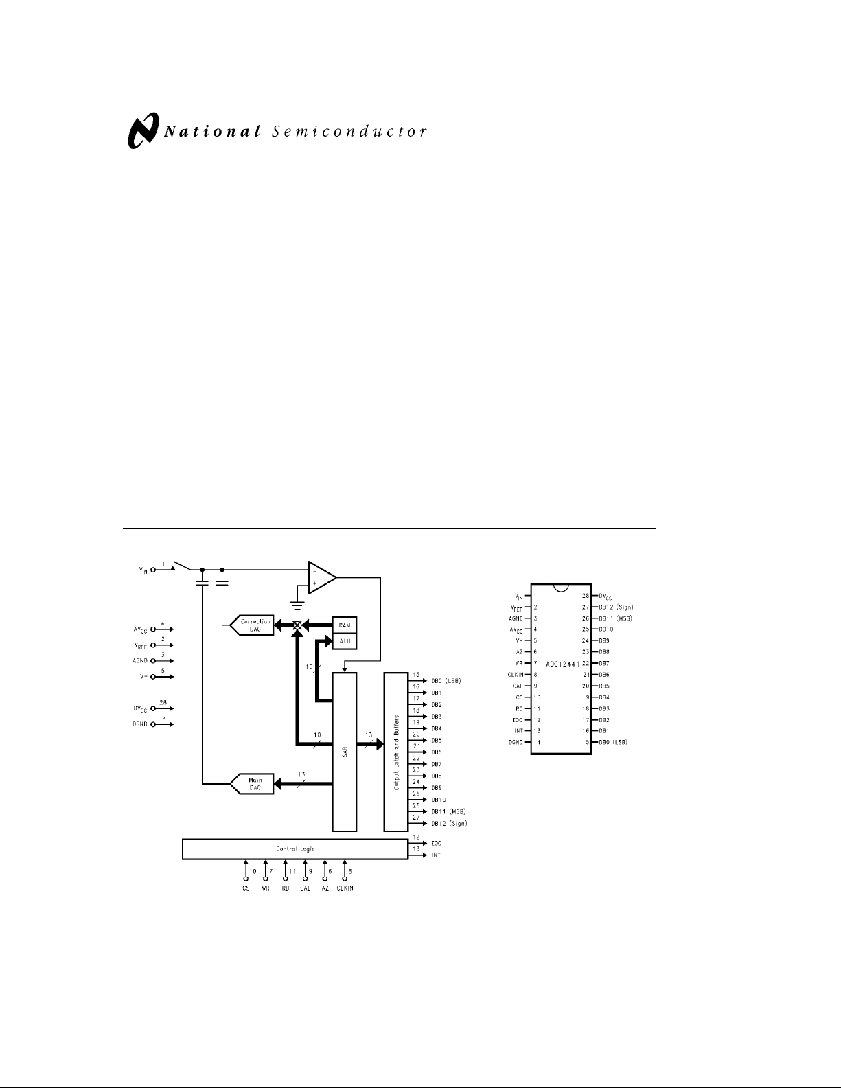
Simplified Block Diagram
Applications
Y
Digital signal processing
Y
Telecommunications
Y
Audio
Y
High resolution process control
Y
Instrumentation
Key Specifications
Y
Resolution 12 bits plus sign
Y
Conversion Time 13.8 ms (max)
Y
Bipolar Signal/Noise 76.5 dB (min)
Y
Total Harmonic Distortion
Y
Aperture Time 100 ns
Y
Aperture Jitter 100 ps
Y
Zero Error
Y
Positive Full Scale Error
Y
Power Consumption
Y
Sampling rate 55 kHz (max)
TRI-STATEÉis a registered trademark of National Semiconductor Corporation.
@
g
5V 70 mW (max)
b
75 dB (max)
g
1 LSB (max)
g
1 LSB (max)
Connection Diagram
Dual-In-Line Package
rms
Top View
TL/H/11017– 2
Order Number
ADC12441CMJ, ADC12441CMJ/883
or ADC12441CIJ
See NS Package Number J28A
TL/H/11017– 1
C
1995 National Semiconductor Corporation RRD-B30M115/Printed in U. S. A.
TL/H/11017
Page 2
Absolute Maximum Ratings (Notes1&2)
If Military/Aerospace specified devices are required,
please contact the National Semiconductor Sales
Office/Distributors for availability and specifications.
Supply Voltage (V
Negative Supply Voltage (Vb)
Voltage at Logic Control Inputs
Voltage at Analog Inputs
(V
and V
IN
AVCC–DVCC(Note 7) 0.3V
Input Current at Any Pin (Note 3)
Package Input Current (Note 3)
Power Dissipation at 25
Storage Temperature Range
ESD Susceptability (Note 5) 2000V
Soldering Information
J Package (10 sec.) 300
e
e
DV
CC
)(V
REF
AVCC) 6.5V
CC
b
0.3V to (V
b
b
0.3V) to (V
C (Note 4) 875 mW
§
a
CC
a
CC
g
g
b
65§Ctoa150§C
b
6.5V
0.3V)
0.3V)
5mA
20 mA
§
Operating Ratings (Notes1&2)
Temperature Range T
ADC12441CIJ
ADC12441CMJ,
ADC12441CMJ/883
DVCCand AVCCVoltage
(Notes6&7) 4.5V to 5.5V
Negative Supply Voltage (V
Reference Voltage
(V
, Notes6&7) 3.5V to AV
REF
C
s
s
T
MIN
b
40§CsT
b
55§CsT
b
)
b
T
A
MAX
s
a
85§C
A
s
a
125§C
A
4.5V tob5.5V
a
50 mV
CC
Converter Electrical Characteristics
The following specifications apply for V
Impedance
all other limits T
e
600X, and f
e
A
e
CLK
e
T
25§C. (Notes 6, 7 and 8)
J
e
e
AV
CC
ea
DV
CC
2.0 MHz unless otherwise specified. Boldface limits apply for T
CC
Symbol Parameter Conditions
5.0V, V
b
eb
5.0V, V
ea
REF
5.0V, Analog Input Source
e
A
Typical Limit Units
(Note 9) (Note 10) (Limit)
STATIC CHARACTERISTICS
Positive Integral Linearity Error After Auto-Cal (Notes 11 & 12)
Negative Integral Linearity Error After Auto-Cal (Notes 11 & 12)
g
(/2 LSB
g
*/4 LSB
Positive or Negative Differential Linearity After Auto-Cal (Notes 11 & 12) 12 Bits
Zero Error After Auto-Zero or Auto-Cal
(Notes 12 & 13)
Positive Full-Scale Error After Auto-Cal (Note 12)
g
(/2
Negative Full-Scale Error After Auto-Cal (Note 12)
V
Analog Input Voltage V
IN
e
Power Supply Zero Error (Note 14) AV
Sensitivity
Full-Scale Error
V
CC
REF
e
4.75V, V
DV
CC
e
5Vg5%,
b
eb
5Vg5%
Linearity Error
C
REFVREF
C
IN
Input Capacitance (Note 18) 80 pF
Analog Input Capacitance 65 pF
V
g
(/8 LSB
g
(/8 LSB
g
(/8 LSB
DYNAMIC CHARACTERISTICS
Bipolar Effective Bits f
(Note 17)
Unipolar Effective Bits f
(Note 17)
S/N Bipolar Signal-to-Noise Ratio f
(Note 17)
S/N Unipolar Signal-to-Noise Ratio f
(Note 17)
IN
f
IN
IN
f
IN
IN
f
IN
f
IN
IN
f
IN
f
IN
e
1 kHz, V
e
20 kHz, V
e
1 kHz, V
e
20 kHz, V
e
1 kHz, V
e
10 kHz, V
e
20 kHz, V
e
1 kHz, V
e
10 kHz, V
e
20 kHz, V
e
g
4.85V 12.6 Bits
IN
e
g
4.85V 12.6 12.4 Bits (min)
IN
e
4.85 V
IN
IN
IN
IN
IN
IN
IN
IN
p-p
e
4.85 V
e
g
4.85V 78 dB
e
g
4.85V 78 dB
e
g
4.85V 78 76.5 dB (min)
e
4.85 V
p-p
e
4.85 V
e
4.85 V
11.8 Bits
11.8 11.6 Bits (min)
p-p
73 dB
p-p
p-p
73 dB
73 71.5 dB (min)
e
T
T
J
MIN
g
1 LSB (max)
g
1 LSB (max)
g1/g
2 LSB (max)
b
b
0.05 V(min)
a
0.05 V(max)
CC
to T
MAX
;
2
Page 3
Converter Electrical Characteristics
The following specifications apply for V
Impedance
all other limits T
e
600X, and f
e
A
e
CLK
e
T
25§C. (Notes 6, 7 and 8) (Continued)
J
e
e
DV
CC
2.0 MHz unless otherwise specified. Boldface limits apply for T
CC
AV
CC
ea
5.0V, V
b
Symbol Parameter Conditions
DYNAMIC CHARACTERISTICS (Continued)
THD Bipolar Total Harmonic Distortion f
(Note 17)
THD Unipolar Total Harmonic Distortion f
(Note 17)
Bipolar Peak Harmonic or f
Spurious Noise (Note 17)
Unipolar Peak Harmonic or f
Spurious Noise (Note 17)
Bipolar Two Tone Intermodulation V
Distortion (Note 17) f
Unipolar Two Tone Intermodulation V
Distortion (Note 17) f
b
3 dB Bipolar Full Power Bandwidth V
b
3 dB Unipolar Full Power Bandwidth V
e
IN
e
f
IN
e
IN
e
f
IN
e
IN
e
f
IN
e
f
IN
e
IN
e
f
IN
e
f
IN
e
IN
e
IN2
e
IN
e
IN2
e
IN
e
IN
1 kHz, V
19.688 kHz, V
1 kHz, V
19.688 kHz, V
1 kHz, V
10 kHz, V
20 kHz, V
1 kHz, V
10 kHz, V
20 kHz, V
g
20.625 kHz
4.85 V
20.625 kHz
g
4.85 V
e
g
IN
IN
e
4.85 V
IN
IN
e
g
IN
e
IN
e
IN
e
4.85 V
IN
e
IN
e
IN
IN1
p-p,fIN1
e
4.85V, f
4.85V (Note 17) 25 20 kHz (Min)
(Note 17) 30 20 kHz (Min)
p-p
Aperture Time 100 ns
Aperture Jitter 100 ps
eb
5.0V, V
4.85V
e
g
4.85V
p-p
e
4.85 V
4.85V
g
4.85V
g
4.85V
p-p
4.85 V
p-p
4.85 V
p-p
19.375 kHz,
e
19.375 kHz,
ea
REF
5.0V, Analog Input Source
e
e
T
A
T
J
MIN
Typical Limit Units
(Note 9) (Notes 10, 19) (Limit)
b
82 dB
p-p
b
80
b
82 dB
b
80
b
88 dB
b
84 dB
b
80 dB
b
90 dB
b
86 dB
b
82 dB
b
78
b
78
b
75 dB (max)
b
75 dB (max)
b
74 dB (max)
b
73 dB (max)
to T
MAX
;
rms
Digital and DC Electrical Characteristics
The following specifications apply for DV
otherwise specified. Boldface limits apply for T
(Notes 6 and 7)
CC
e
ea
AV
A
CC
5.0V, V
e
e
T
T
J
MIN
Symbol Parameter Conditions
V
IN(1)
V
IN(0)
I
IN(1)
I
IN(0)
V
T
V
T
V
H
V
OUT(1)
V
OUT(0)
Logical ‘‘1’’ Input Voltage for V
All Inputs except CLK IN
Logical ‘‘0’’ Input Voltage for V
All Inputs except CLK IN
Logical ‘‘1’’ Input Current V
Logical ‘‘0’’ Input Current V
a
CLK IN Positive-Going
Threshold Voltage
b
CLK IN Negative-Going
Threshold Voltage
CLK IN Hysteresis
[
V
a
(min)bV
T
b
]
(max)
T
Logical ‘‘1’’ Output Voltage V
Logical ‘‘0’’ Output Voltage V
e
5.25V
CC
e
4.75V
CC
e
5V 0.005 1 mA (max)
IN
e
0V
IN
e
4.75V:
CC
eb
I
I
CC
360 mA 2.4 V (min)
OUT
eb
10 mA 4.5 V (min)
OUT
e
4.75V, I
OUT
3
b
to T
eb
MAX
5.0V, V
; all other limits T
REF
ea
5.0V, and f
e
T
A
J
e
CLK
25§C.
e
2.0 MHz unless
Typical Limit Units
(Note 9) (Notes 10, 19) (Limits)
2.0 V (min)
0.8 V (max)
b
0.005
b
1 mA (max)
2.8 2.7 V (min)
2.1 2.3 V (max)
0.7 0.4 V (min)
e
1.6 mA 0.4 V (max)
Page 4
Digital and DC Electrical Characteristics
The following specifications apply for DV
otherwise specified. Boldface limits apply for T
(Notes 6 and 7) (Continued)
CC
e
ea
AV
A
CC
5.0V, V
e
e
T
T
J
MIN
Symbol Parameter Conditions
I
OUT
I
SOURCE
I
SINK
DI
CC
AI
CC
b
I
TRI-STATEÉOutput Leakage V
Current
Output Source Current V
Output Sink Current V
DVCCSupply Current f
AVCCSupply Current f
VbSupply Current f
e
0V
OUT
e
V
5V 0.01 3 mA (max)
OUT
e
0V
OUT
e
5V 20 8.0 mA (min)
OUT
e
2 MHz, CSe‘‘1’’ 1 2 mA (max)
CLK
e
2 MHz, CSe‘‘1’’ 2.8 6 mA (max)
CLK
e
2 MHz, CSe‘‘1’’ 2.8 6 mA (max)
CLK
b
to T
eb
MAX
REF
ea
5.0V, V
; all other limits T
5.0V, and f
e
T
A
e
CLK
e
25§C.
J
Typical Limit Units
(Note 9) (Notes 10, 19) (Limits)
b
0.01
b
20
b
3 mA (max)
b
6.0 mA (min)
2.0 MHz unless
AC Electrical Characteristics
The following specifications apply for DV
Boldface limits apply for T
e
T
A
J
e
ea
AV
CC
e
T
MIN
to T
CC
MAX
; all other limits T
Symbol Parameter Conditions
f
CLK
Clock Frequency
5.0V, V
b
eb
e
A
e
5.0V, t
T
t
r
e
25§C. (Notes 6 and 7)
J
e
20 ns unless otherwise specified.
f
Typical Limit Units
(Note 9) (Notes 10, 19) (Limits)
0.5 MHz (min)
4.0 2.0 MHz (max)
Clock Duty Cycle 50 %
40 % (min)
60 % (max)
t
C
t
A
t
Z
t
CAL
t
W(CAL)L
t
W(WR)L
t
ACC
t0H,t
t
PD(INT)
Note 1: Absolute Maximum Ratings indicate limits beyond which damage to the device may occur. Operating Ratings indicate conditions for which the device is
functional, but do not guarantee specific performance limits. For guaranteed specifications and test conditions, see the Electrical Characteristics. The guaranteed
specifications apply only for the test conditions listed. Some performance characteristics may degrade when the device is not operated under the listed test
conditions.
Note 2: All voltages are measured with respect to AGND and DGND, unless otherwise specified.
Note 3: When the input voltage (V
5 mA. The 20 mA maximum package input current rating allows the voltage at any four pins, with an input current limit of 5 mA, to simultaneously exceed the power
supply voltages.
Conversion Time 27(1/f
e
f
2.0 MHz 13.5 ms
CLK
Acquisition Time R
(Note 15)
f
CLK
SOURCE
e
e
50X 7(1/f
2.0 MHz
Auto Zero Time 26(1/f
e
f
2.0 MHz 13 ms
CLK
Calibration Time 1396(1/f
e
f
2.0 MHz 698 706 ms (max)
CLK
) 27(1/f
CLK
) 7(1/f
CLK
)a300 ns (max)
CLK
)a300 ns (max)
CLK
3.5 ms
) 26(1/f
CLK
) max
CLK
) (max)
CLK
Calibration Pulse Width (Note 16) 60 200 ns (min)
Minimum WR Pulse Width 60 200 ns (min)
Maximum Access Time C
(Delay from Falling Edge of 50 85 ns (max)
RD
to Output Data Valid)
TRI-STATE Control R
1H
(Delay from Rising Edge of C
RD
to Hi-Z State)
Maximum Delay from Falling Edge of
RD
or WR to Reset of INT
) at any pin exceeds the power supply rails (V
IN
e
100 pF
L
e
1kX,
L
e
100 pF 30 90 ns (max)
L
100 175 ns (max)
k
IN
Vbor V
l
(AVCCor DVCC), the current at that pin should be limited to
IN
4
Page 5
AC Electrical Characteristics (Continued)
Note 4: The power dissipation of this device under normal operation should never exceed 169 mW (Quiescent Power DissipationaTTL Loads on the digital
outputs). Caution should be taken not to exceed absolute maximum power rating when the device is operating in a severe fault condition (ex. when any inputs or
outputs exceed the power supply). The maximum power dissipation must be derated at elevated temperatures and is dictated by T
temperature), i
is P
Dmax
resistance (i
Note 5: Human body model, 100 pF discharged through a 1.5 kX resistor.
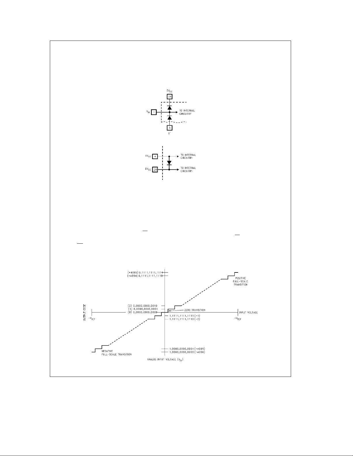
Note 6: Two on-chip diodes are tied to the analog input as shown below. Errors in the A/D conversion can occur if these diodes are forward biased more than
50 mV.
(package junction to ambient thermal resistance), and TA(ambient temperature). The maximum allowable power dissipation at any temperature
JA
e
b
(T
TA)/iJAor the number given in the Absolute Maximum Ratings, whichever is lower. For this device, T
Jmax
) of the ADC12441 with CMJ and CIJ suffixes when board mounted is 47§C/W.
JA
Jmax
e
(maximum junction
Jmax
125§C, and the typical thermal
This means that if AVCCand DVCCare minimum (4.75 VDC) and Vbis maximum (b4.75 VDC), full-scale must bes4.8 VDC.
Note 7: A diode exists between AV
To guarantee accuracy, it is required that the AVCCand DVCCbe connected together to a power supply with separate bypass filters at each VCCpin.
Note 8: Accuracy is guaranteed at f
Characteristics section.
Note 9: Typicals are at T
Note 10: Limits are guaranteed to National’s AOQL (Average Outgoing Quality Level).
Note 11: Positive linearity error is defined as the deviation of the analog value, expressed in LSBs, from the straight line that passes through positive full scale and
zero. For negative linearity error the straight line passes through negative full scale and zero. (See
Note 12: The ADC12441’s self-calibration technique ensures linearity, full scale, and offset errors as specified, but noise inherent in the self-calibration process will
result in a repeatability uncertainty of
Note 13: If T
Note 14: After an Auto-Zero or Auto-Cal cycle at the specified power supply extremes.
Note 15: If the clock is asynchronous to the falling edge of WR
t
periods.
Note 16: The CAL
Note 17: The specifications for these parameters are valid after an Auto-Cal cycle has been completed.
Note 18: The ADC12441 reference ladder is composed solely of capacitors.
Note 19: A Military RETS Electrical Test Specification is available on request. At time of printing the ADC12441CMJ/883 RETS complies fully with the boldface
limits in this column.
A
e
6 clock periods and the maximum t
A
J
changes then an Auto-Zero or Auto-Cal cycle will have to be re-started (see the Typical Performance Characteristic curves).
line must be high before a conversion is started.
and DVCCas shown below.
CC
e
2.0 MHz. At higher and lower clock frequencies accuracy may degrade. See curves in the Typical Performance
CLK
e
25§C and represent most likely parametric norm.
g
0.20 LSB.
e
7 clock periods. If the falling edge of the clock is synchronous to the rising edge of WR then tAwill be exactly 6.5 clock
A
an uncertainty of one clock period will exist in the interval of tA, therefore making the minimum
TL/H/11017– 3
TL/H/11017– 4
Figures 1b
and1c.)
FIGURE 1a. Transfer Characteristic
5
TL/H/11017– 5
Page 6

Electrical Characteristics (Continued)
FIGURE 1b. Simplified Error Curve vs Output Code without Auto-Cal or Auto-Zero Cycles
FIGURE 1c. Simplified Error Curve vs Output Code after Auto-Cal Cycle
Typical Performance Characteristics
Zero Error vs V
REF
TL/H/11017– 6
TL/H/11017– 7
Zero Error Change vs
Ambient Temperature
TL/H/11017– 8
6
Page 7

Typical Performance Characteristics (Continued)
Linearity Error vs V
Bipolar Signal-to-
a
Distortion Ratio vs
Noise
Input Frequency
Bipolar Signal-to-
a
Distortion Ratio vs
Noise
Input Signal Level
REF
Linearity Error vs Clock
Frequency
Unipolar Signal-to-
a
Distortion Ratio vs
Noise
Input Frequency
Unipolar Signal-to-
a
Distortion Ratio vs
Noise
Input Signal Level
Full Scale Error Change vs
Ambient Temperature
Bipolar Signal-to-
a
Distortion Ratio vs
Noise
Input Source Impedance
Bipolar Spectral Response
with 10 kHz Sine Wave Input
Bipolar Spectral Response
with 1 kHz Sine Wave Input
Unipolar Spectral Response
with 1 kHz Sine Wave Input
7
Unipolar Spectral Response
with 10 kHz Sine Wave Input
TL/H/11017– 9
Page 8

Typical Performance Characteristics (Continued)
Bipolar Spectral Response
with 20 kHz Sine Wave Input
Unipolar Spectral Response
with 20 kHz Sine Wave Input
Test Circuits
Timing Diagrams
TL/H/11017– 10
TL/H/11017– 12
TL/H/11017– 14
FIGURE 2. TRI-STATE Test Circuits and Waveforms
Auto-Cal Cycle (CSe1, WReX, RDeX, AZeX, XeDon’t Care)
TL/H/11017– 11
TL/H/11017– 13
TL/H/11017– 15
TL/H/11017– 16
8
Page 9

Timing Diagrams (Continued)
Normal Conversion with Auto-Zero (CAL
Normal Conversion without Auto-Zero (CALe1, AZe1)
e
1, AZe0)
TL/H/11017– 17
TL/H/11017– 18
9
Page 10

1.0 Pin Descriptions
DVCC(28),
AV
CC
Vb(5) The analog negative supply voltage pin. V
DGND (14), The digital and analog ground pins. AGND
AGND (3) and DGND must be connected together ex-
V
REF
V
(1) The analog input voltage pin. To guarantee
IN
(10) The Chip Select control input. This input is
CS
RD
(11) The Read control input. With both CS and RD
WR (7) The Write control input. The converison is
CLK (8) The external clock input pin. The clock fre-
CAL
(9) The Auto-Calibration control input. When
AZ
(6) The Auto-Zero control input. With the AZ pin
EOC (12) The End-of-Conversion control output. This
INT
(13) The Interrupt control output. This output goes
The digital and analog positive power supply
(4)
pins. The digital and analog power supply
voltage range of the ADC12441 isa4.5V to
a
5.5V. To guarantee accuracy, it is required
that the AV
gether to the same power supply with sepa-
and DVCCbe connected to-
CC
rate bypass filters (10 mF tantalum in parallel
with a 0.1 mF ceramic) at each V
CC
pin.
has a range ofb4.5V tob5.5V and needs a
bypass filter of 10 mF tantalum in parallel with
a 0.1 mF ceramic.
ternally to guarantee accuracy.
(2) The reference input voltage pin. To maintain
accuracy the voltage at this pin should not
exceed the AV
50 mV or go below 3.5 VDC.
or DVCCby more than
CC
accuracy the voltage at this pin should not
exceed V
b
V
active low and enables the WR
by more than 50 mV or go below
CC
by more than 50 mV.
and RD func-
tions.
low the TRI-STATE output buffers are enabled and the INT
started on the rising edge of the WR
when CS
output is reset high.
pulse
is low.
quency range is 500 kHz to 4 MHz.
CAL
is low the ADC12441 is reset and a calibration cycle is initiated. During the calibration cycle the values of the comparator offset
voltage and the mismatch errors in the capacitor reference ladder are determined and
stored in RAM. These values are used to correct the errors during a normal cycle of A/D
conversion.
held low during a conversion, the ADC12441
goes into an auto-zero cycle before the actual A/D conversion is started. This Auto-Zero
cycle corrects for the comparator offset voltage. The total conversion time (t
creased by 26 clock periods when Auto-Zero
)isin-
C
is used.
output is low during a conversion or a calibration cycle.
low when a conversion has been completed
and indicates that the conversion result is
available in the output latches. Reading the
result or starting a conversion or calibration
cycle will reset this output high.
DB0–DB12
(15–27)
The TRI-STATE output pins. The output is in
two’s complement format with DB12 the sign
bit, DB11 the MSB and DB0 the LSB.
2.0 Functional Description
The ADC12441 is a 12-bit plus sign A/D converter with the
capability of doing Auto-Zero or Auto-Cal routines to minimize zero, full-scale and linearity errors. It is a successive-
b
approximation A/D converter consisting of a DAC, comparator and a successive-approximation register (SAR). AutoZero is an internal calibration sequence that corrects for the
A/D’s zero error caused by the comparator’s offset voltage.
Auto-Cal is a calibration cycle that not only corrects zero
error but also corrects for full-scale and linearity errors
caused by DAC inaccuracies. Auto-Cal minimizes the errors
of the ADC12441 without the need of trimming during its
fabrication. An Auto-Cal cycle can restore the accuracy of
the ADC12441 at any time, which ensures its long term stability.
2.1 DIGITAL INTERFACE
On power up, a calibration sequence should be initiated by
pulsing CAL
edge the CAL
CAL
clock periods. During the calibration sequence, first the
comparator’s offset is determined, then the capacitive
DAC’s mismatch error is found. Correction factors for these
errors are then stored in internal RAM.
A conversion is initiated by taking CS
(Auto Zero) signal line should be tied high or low during the
conversion process. If AZ
takes approximately 26 clock periods, occurs before the actual conversion is started. The auto zero cycle determines
the correction factors for the comparator’s offset voltage. If
AZ
input is sampled for 7 clock periods, and held in the capacitive DAC’s ladder structure. The EOC then goes low, signaling that the analog input is no longer being sampled and
that the A/D successive approximation conversion has
started.
During a conversion, the sampled input voltage is successively compared to the output of the DAC. First, the acquired input voltage is compared to analog ground to determine its polarity. The sign bit is set low for positive input
voltages and high for negative. Next the MSB of the DAC is
set high with the rest of the bits low. If the input voltage is
greater than the output of the DAC, then the MSB is left
high; otherwise it is set low. The next bit is set high, making
the output of the DAC three quarters or one quarter of full
scale. A comparison is done and if the input is greater than
the new DAC value this bit remains high; if the input is less
than the new DAC value the bit is set low. This process
continues until each bit has been tested. The result is then
stored in the output latch of the ADC12441. Next EOC goes
high, and INT
The result can now be read by taking CS
enable the DB0 –DB12 output buffers.
low with CS,RD, and WR high. To acknowl-
signal, EOC goes low after the falling edge of
, and remains low during the calibration cycle of 1396
is low an auto zero cycle, which
is high, the auto zero cycle is skipped. Next the analog
goes low to signal the end of the conversion.
and WR low. The AZ
and RD low to
10
Page 11

2.0 Functional Description (Continued)
Digital Control Inputs
CS WR RD CAL AZ
ßß 1 1 1 Start Conversion without Auto-Zero
ß 1 ß 1 1 Read Conversion Result without Auto-Zero
ßß 1 1 0 Start Conversion with Auto-Zero
ß 1 ß 1 0 Read Conversion Result with Auto-Zero
1XXßX Start Calibration Cycle
0 X 1 0 X Test Mode (DB2, DB3, DB5 and DB6 become active)
FIGURE 1. Function of the A/D Control Inputs
The table in
control inputs on the function of the ADC12441. The Test
Mode, where RD
during manufacture to thoroughly check out the operation of
the ADC12441. Care should be taken not to inadvertently
be in this mode, since DB2, DB3, DB5, and DB6 become
active outputs, which may cause data bus contention.
2.2 RESETTING THE A/D
All internal logic can be reset, which will abort any conversion in process. The A/D is reset whenever a new conversion is started by taking CS
the analog input is being sampled or when EOC is low, the
Auto-Cal correction factors may be corrupted, therefore requiring an Auto-Cal cycle before the next conversion. This is
true with or without Auto-Zero. The Calibration Cycle cannot
be reset once started. On power-up the ADC12441 automatically goes through a Calibration Cycle that takes typically 1396 clock cycles. For reasons that will be discussed
in Section 3.7, a new calibration cycle needs to be started
after the completion of the automatic one.
Figure 1
summarizes the effect of the digital
is high and CS and CAL are low, is used
and WR low. If this is done when
A/D Function
3.0 Analog Considerations
3.1 REFERENCE VOLTAGE
The voltage applied to the reference input of the converter
defines the voltage span of the analog input (the difference
between V
codes and 4096 negative output codes exist. The A-to-D
can be used in either ratiometric or absolute reference applications. The voltage source driving V
very low output impedance and very low noise. The circuit in
Figure 2a
appropriate for use with the ADC12441. The simple reference circuit of
does not require low full scale errors.
In a ratiometric system, the analog input voltage is proportional to the voltage used for the A/D reference. When this
voltage is the system power supply, the V
tied to V
of the system reference as the analog input and A/D reference move together maintaining the same output code for
given input condition.
and AGND), over which 4095 positive output
IN
must have a
REF
is an example of a very stable reference that is
Figure 2b
. This technique relaxes the stability requirement
CC
may be used when the application
pin can be
REF
FIGURE 2a. Low Drift Extremely Stable Reference Circuit
Errors without any trims:
Full Scale
Zero
Linearity
TL/H/11017– 20
FIGURE 2b. Simple Reference Circuit
11
*Tantalum
**Ceramic
C
25
§
g
0.075%
g
0.024%
g
(/2 LSB
TL/H/11017– 19
b
40§Ctoa85§C
g
0.2%
g
0.024%
g
(/2 LSB
Page 12

3.0 Analog Considerations (Continued)
For absolute accuracy, where the analog input varies between very specific voltage limits, the reference pin can be
biased with a time and temperature stable voltage source.
In general, the magnitude of the reference voltage will require an initial adjustment to null out full-scale errors.
3.2 INPUT CURRENT
Because the input network of the ADC12441 is made up of
a switch and a network of capacitors, a charging current will
flow into or out of (depending on the input voltage polarity)
of the analog input pin (V
sampling period (t
pend on the actual input voltage applied.
3.3 NOISE
The leads to the analog input pin should be kept as short as
possible to minimize input noise coupling. Both noise and
undesired digital clock coupling to this input can cause errors. Input filtering can be used to reduce the effects of
these noise sources.
3.4 INPUT BYPASS CAPACITORS
An external capacitor can be used to filter out any noise due
to inductive pickup by a long input lead and will not degrade
the accuracy of the conversion result.
3.5 INPUT SOURCE RESISTANCE
The analog input can be modeled as shown in
External R
voltage on C
input voltage. With f
3.5 ms, R
settle properly.
will lengthen the time period necessary for the
S
REF
s
1kXwill allow a 5V analog input voltage to
S
3.6 POWER SUPPLIES
Noise spikes on the V
conversion errors as the comparator will respond to this
noise. The A/D is especially sensitive during the auto-zero
or auto-cal procedures to any power supply spikes. Low in
ductance tantalum capacitors of 10 mF or greater paralleled
) on the start of the analog input
IN
). The peak value of this current will de-
A
Figure 3
to settle to within (/2 LSB of the analog
e
2 MHz t
CLK
and Vbsupply lines can cause
CC
e
7 clock periods
A
with 0.1 mF ceramic capacitors are recommended for supply
bypassing. Separate bypass capacitors whould be placed
close to the DV
voltage source is available in the system, a separate
,AVCCand Vbpins. If an unregulated
CC
LM340LAZ-5.0 voltage regulator for the A-to-D’s V
other analog circuitry) will greatly reduce digital noise on the
supply line.
3.7 THE CALIBRATION CYCLE
On power up the ADC12441 goes through an Auto-Cal cycle which cannot be interrupted. Since the power supply,
reference, and clock will not be stable at power up, this first
calibration cycle will not result in an accurate calibration of
the A/D. A new calibration cycle needs to be started after
the power supplies, reference, and clock have been given
enough time to stabilize. During the calibration cycle, correction values are determined for the offset voltage of the
sampled data comparator and any linearity and gain errors.
These values are stored in internal RAM and used during an
analog-to-digital conversion to bring the overall full scale,
offset, and linearity errors down to the specified limits. Full
scale error typically changes
g
0.1 LSB over temperature
and linearity error changes even less; therefore it should be
necessary to go through the calibration cycle only once after power up, if auto-zero is used to correct the zero error
change.
.
3.8 THE AUTO-ZERO CYCLE
To correct for any change in the zero (offset) error of the
A/D, the auto-zero cycle can be used. It may be necessary
e
to do an auto-zero cycle whenever the ambient temperature
changes significantly. (See the curved titled ‘‘Zero Error
Change vs Ambient Temperature’’ in the Typical Performance Characteristics.) A change in the ambient temperature
will cause the V
change, which may cause the zero error of the A/D to be
greater than
zero error to
of the sampled data comparator to
OS
g
1 LSB. An auto-zero cycle will maintain the
g
1 LSB or less.
CC
(and
FIGURE 3. Analog Input Equivalent Circuit
12
TL/H/11017– 21
Page 13

4.0 Dynamic Performance
Many applications require the A/D converter to digitize ac
signals, but the standard dc integral and differential nonlinearity specifications will not accurately predict the A/D converter’s performance with ac input signals. The important
specifications for ac applications reflect the converter’s ability to digitize ac signals without significant spectral errors
and without adding noise to the digitized signal. Dynamic
characteristics such as signal-to-noise ratio (S/N), signal-to-
a
noise
distortion ratio (S/(NaD)), effective bits, full power
bandwidth, aperture time and aperture jitter are quantitative
measures of the A/D converter’s capability.
An A/D converter’s ac performance can be measured using
Fast Fourier Transform (FFT) methods. A sinusoidal waveform is applied to the A/D converter’s input, and the transform is then performed on the digitized waveform. S/(N
and S/N are calculated from the resulting FFT data, and a
spectral plot may also be obtained. Typical values for S/N
are shown in the table of Electrical Characteristics, and
spectral plots of S/(N
a
D) are included in the typical per-
formance curves.
The A/D converter’s noise and distortion levels will change
with the frequency of the input signal, with more distortion
and noise occurring at higher signal frequencies. This can
be seen in the S/(N
curves will also give an indication of the full power bandwidth (the frequency at which the S/(N
a
D) versus frequency curves. These
a
D) or S/N drops
3 dB).
Effective number of bits can also be useful in describing the
A/D’s noise performance. An ideal A/D converter will have
some amount of quantization noise, determined by its resolution, which will yield an optimum S/N ratio given by the
following equation:
e
S/N
(6.02cna1.8)dB
where n is the A/D’s resolution in bits.
The effective bits of a real A/D converter, therefore, can be
found by:
S/N(dB)b1.8
n(effective)
As an example, an ADC12441 with a
e
6.02
g
5V, 10 kHz sine
wave input signal will typically have a S/N of 78 dB, which is
equivalent to 12.6 effective bits.
Two sample/hold specifications, aperture time and aperture
jitter, are included in the Dynamic Characteristics table
since the ADC12441 has the ability to track and hold the
analog input voltage. Aperture time is the delay for the A/D
a
to respond to the hold command. In the case of the
ADC12441, the hold command is internally generated.
When the Auto-Zero function is not being used, the hold
command occurs at the end of the acquisition window, or
seven clock periods after the rising edge of the WR
delay between the internally generated hold command and
the time that the ADC12441 actually holds the input signal is
the aperture time. For the ADC12441, this time is typically
100 ns. Aperture jitter is the change in the aperture time
from sample to sample. Aperture jitter is useful in determining the maximum slew rate of the input signal for a given
accuracy. For example, an ADC12441 with 100 ps of aperture jitter operating with a 5V reference can have an effective gain variation of about 1 LSB with an input signal whose
slew rate is 12 V/ms.
D)
Power Supply Bypassing
*Tantalum
**Ceramic
Protecting the Analog Inputs
Note: External protection diodes should be able to withstand the op amp
current limit.
. The
TL/H/11017– 22
TL/H/11017– 23
13
Page 14

Physical Dimensions inches (millimeters)
Order Number ADC12441CMJ, ADC12441CMJ/883, or ADC12441CIJ
NS Package Number J28A
Plus Sign A/D Converter with Sample-and-Hold
ADC12441 Dynamically-Tested Self-Calibrating 12-Bit
LIFE SUPPORT POLICY
NATIONAL’S PRODUCTS ARE NOT AUTHORIZED FOR USE AS CRITICAL COMPONENTS IN LIFE SUPPORT
DEVICES OR SYSTEMS WITHOUT THE EXPRESS WRITTEN APPROVAL OF THE PRESIDENT OF NATIONAL
SEMICONDUCTOR CORPORATION. As used herein:
1. Life support devices or systems are devices or 2. A critical component is any component of a life
systems which, (a) are intended for surgical implant support device or system whose failure to perform can
into the body, or (b) support or sustain life, and whose be reasonably expected to cause the failure of the life
failure to perform, when properly used in accordance support device or system, or to affect its safety or
with instructions for use provided in the labeling, can effectiveness.
be reasonably expected to result in a significant injury
to the user.
National Semiconductor National Semiconductor National Semiconductor National Semiconductor
Corporation Europe Hong Kong Ltd. Japan Ltd.
1111 West Bardin Road Fax: (
Arlington, TX 76017 Email: cnjwge@tevm2.nsc.com Ocean Centre, 5 Canton Rd. Fax: 81-043-299-2408
Tel: 1(800) 272-9959 Deutsch Tel: (
Fax: 1(800) 737-7018 English Tel: (
National does not assume any responsibility for use of any circuitry described, no circuit patent licenses are implied and National reserves the right at any time without notice to change said circuitry and specifications.
Fran3ais Tel: (
Italiano Tel: (
a
49) 0-180-530 85 86 13th Floor, Straight Block, Tel: 81-043-299-2309
a
49) 0-180-530 85 85 Tsimshatsui, Kowloon
a
49) 0-180-532 78 32 Hong Kong
a
49) 0-180-532 93 58 Tel: (852) 2737-1600
a
49) 0-180-534 16 80 Fax: (852) 2736-9960
 Loading...