

Page 1
ADC1205/ADC1225 12-Bit Plus Sign
mP Compatible A/D Converters
General Description
The ADC1205 and ADC1225 are CMOS, 12-bit plus sign
successive approximation A/D converters. The 24-pin
ADC1205 outputs the 13-bit data result in two 8-bit bytes,
formatted high-byte first with sign extended. The 28-pin
ADC1225 outputs a 13-bit word in parallel for direct interface to a 16-bit data bus.
Negative numbers are represented in 2’s complement data
format. All digital signals are fully TTL and MOS compatible.
A unipolar input (0V to 5V) can be accommodated with a
single 5V supply, while a bipolar input (
b
5V toa5V) re-
quires the addition of a 5V negative supply.
The ADC1205C and ADC1225C have a maximum non-linearity of 0.0224% of Full Scale.
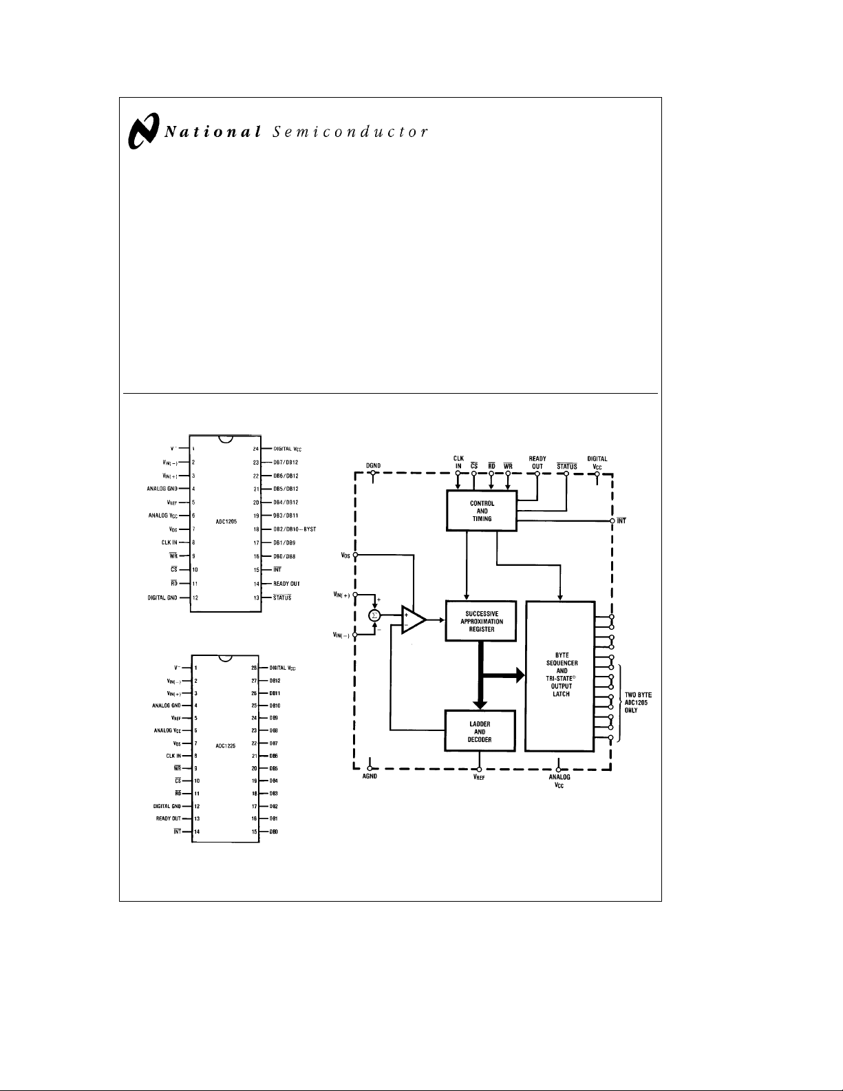
Connection and Functional Diagrams
Dual-In-Line Package
Key Specifications
Y
ResolutionÐ12 bits plus sign
Y
Linearity ErrorÐg1 LSB
Y
Conversion TimeÐ100 ms
Features
Y
Compatible with all mPs
Y
True differential analog voltage inputs
Y
0V to 5V analog voltage range with single 5V supply
Y
TTL/MOS input/output compatible
Y
Low powerÐ25 mW max
Y
Standard 24-pin or 28-pin DIP
ADC1205/ADC1225 12-Bit Plus Sign mP Compatible A/D Converters
June 1994
Top View
TL/H/5676– 1
Dual-In-Line Package
TL/H/5676– 3
See Ordering Information
Top View
TRI-STATEÉis a registered trademark of National Semiconductor Corporation.
C
1995 National Semiconductor Corporation RRD-B30M115/Printed in U. S. A.
TL/H/5676– 2
TL/H/5676
Page 2
Absolute Maximum Ratings (Notes1&2)
If Military/Aerospace specified devices are required,
please contact the National Semiconductor Sales
Office/Distributors for availability and specifications.
Supply Voltage (DV
Negative Supply Voltage (V
Logic Control Inputs
Voltage at Analog Inputs
[
V
IN(a),VIN(b)
Voltage at All Outputs, V
Input Current per Pin
Input Current per Package
Storage Temperature Range
Package Dissipation at T
Lead Temp. (Soldering, 10 seconds) 300
and AVCC) 6.5V
CC
b
)
]
REF,VOS
(V
e
25§C 875 mW
A
b
b
)b0.3V to V
b
0.3V to (V
b
65§Ctoa150§C
b
0.3V toa15V
15V to GND
a
0.3V
CC
a
0.3)V
CC
g
5mA
g
20mA
§
Operating Conditions (Notes1&2)
Temperature Range T
ADC1205CCJ, ADC1225CCD
ADC1205CCJ-1, ADC1225CCD-1 0
Supply Voltage (DV
Negative Supply Voltage (Vb)
C
and AVCC) 4.5 VDCto 6.0 V
CC
b
40§CsT
s
T
MIN
A
CsT
§
b
15V to GND
s
T
A
MAX
s
a
85§C
s
70§C
A
DC
ESD Susceptibility (Note 12) 800V
Electrical Characteristics
MIN
Typ
(Note 8)
b
eb
5V for bipolar input range, or
to T
; all other limits T
MAX
Tested Design
Limit Limit
g
1
g
2
g
30
g
2
g
2
g
30
g
2
s
IN(a)
s
IN(a)
A
g
1 LSB
g
2 LSB
g
30 LSB
g
(/2 LSB
g
2 LSB
g
2 LSB
g
30 LSB
g
2 LSB
5.05V;
5.05V;
e
Limit
Units
T
J
e
The following specifications apply for DV
b
e
V
GND for unipolar input range unless otherwise specified. Bipolar input range is defined asb5.05VsV
b
5.05VsV
b
0.05VsV
e
25§C (Notes 3, 4, 5, 6, 7).
IN(b)
IN(b)
s
5.05V andlV
s
5.05V andlV
IN(a)
IN(a)
CC
b
b
V
e
AV
5V, V
CC
s
V
IN(b)
5.05V. Unipolar input range is defined asb0.05VsV
l
IN(b)
s
5.05V. Boldface limits apply from T
l
REF
e
5V, f
CLK
e
1.0 MHz, V
ADC1205CCJ, ADC1225CCD ADC1205CCJ-1, ADC1225CCD-1
Parameter Conditions
Typ
(Note 8)
Tested Design
Limit Limit
(Note 9) (Note 10) (Note 9) (Note 10)
CONVERTER CHARACTERISTICS
Linearity Error Unipolar Input
ADC1205CCJ, ADC1225CCD Range
ADC1205CCJ-1, ADC1225CCD-1 (Note 11)
Unadjusted Zero Error Unipolar Input
Unadjusted Positive and Negative Unipolar Input
Full-Scale Error Range
Negative Full-Scale Error Unipolar Input
Linearity Error Bipolar Input
ADC1205CCJ, ADC1225CCD Range
ADC1205CCJ-1, ADC1225CCD-1 (Note 11)
Unadjusted Zero Error Bipolar Input
Unadjusted Positive and Negative Bipolar Input
Full-Scale Error Range
Negative Full-Scale Error Bipolar Input
Maximum Gain Temperature 6 15 6 15 ppm/§C
Coefficient
Maximum Offset Temperature 0.5 1.5 0.5 1.5 ppm/§C
Coefficient
Minimum V
Maximum V
Input Resistance 4.0 2 4.0 2 2 kX
REF
Input Resistance 4.0 8 4.0 8 8 kX
REF
Range
Range, Full
Scale Adj. to
Zero
Range
Range, Full
Scale Adj. to
Zero
g
1 LSB
g
2
g
30
g
(/2
g
2 LSB
g
2
g
30
g
2
2
Page 3
Electrical Characteristics (Continued)
e
e
AV
The following specifications apply for DV
b
e
V
GND for unipolar input range unless otherwise specified. Bipolar input range is defined asb5.05VsV
b
5.05VsV
b
0.05VsV
e
25§C (Notes 3, 4, 5, 6, 7).
IN(b)
IN(b)
s
5.05V andlV
s
5.05V andlV
IN(a)
IN(a)
CC
b
V
IN(b)
b
V
IN(b)
5V, V
CC
s
5.05V. Unipolar input range is defined asb0.05VsV
l
s
5.05V. Boldface limits apply from T
l
REF
e
5V, f
CLK
e
1.0 MHz, V
ADC1205CCJ, ADC1225CCD ADC1205CCJ-1, ADC1225CCD-1
Parameter Conditions
Typ
(Note 8)
Tested Design
Limit Limit
(Note 9) (Note 10) (Note 9) (Note 10)
CONVERTER CHARACTERISTICS (Continued)
Minimum Analog Input Unipolar Input GND-0.05 GND-0.05 GND-0.05 V
Voltage Range
b
Bipolar Input
Range
Maximum Analog Input Unipolar Input V
Voltage Range
Bipolar Input V
Range
DC Common-Mode Error
Power Supply Sensitivity AV
5Vg5%,
V
b
CC
eb
e
DV
5Vg5%
CC
a
0.05 V
CC
g
(/8
e
Zero Error
Positive and Negative
b
V
0.05
CC
a
0.05 V
CC
g
(/2
g
*/4
g
*/4
Full-Scale Error
Linearity Error
g
(/4
DIGITAL AND DC CHARACTERISTICS
V
, Logical ‘‘1’’ Input V
IN(1)
Voltage (Min) All Inputs except
e
5.25V, 2.0 2.0 2.0 V
CC
CLK IN
V
, Logical ‘‘0’’ Input V
IN(0)
Voltage (Max) All Inputs except
e
4.75V, 0.8 0.8 0.8 V
CC
CLK IN
I
, Logical ‘‘1’’ Input V
IN(1)
Current (Max)
I
, Logical ‘‘0’’ Input V
IN(0)
Current (Max)
a
V
(Min), Minimum Positive- CLK IN 3.1 2.7 3.1 2.7 2.7 V
T
Going Threshold Voltage
a
V
(Max), Maximum Positive- CLK IN 3.1 3.5 3.1 3.5 3.5 V
T
Going Threshold Voltage
b
V
(Min), Minimum Negative- CLK IN 1.8 1.4 1.8 1.4 1.4 V
T
Going Threshold Voltage
b
V
(Max), Maximum Negative- CLK IN 1.8 2.1 1.8 2.1 2.1 V
T
Going Threshold Voltage
VH(Min), Minimum Hysteresis CLK IN 1.3 0.6 1.3 0.6 0.6 V
a
[
V
(Min)bV
T
VH(Max), Maximum Hysteresis CLK IN 1.3 2.1 1.3 2.1 2.1 V
a
[
V
(Max)bV
T
T
b
T
(Max)
b
(Min)
]
]
e
5V 0.005 1 0.005 1 mA
IN
e
0V
IN
b
0.005
b
1
b
MIN
Typ
(Note 8)
g
(/8
b
0.005
eb
5V for bipolar input range, or
to T
MAX
IN(a)
IN(a)
; all other limits T
Tested Design
Limit Limit
b
b
V
0.05bV
CC
CC
C
a
a
g
(/2
g
*/4
g
*/4
g
(/4
0.05 V
0.05 V
CC
CC
CC
g
g
g
g
s
5.05V;
s
5.05V;
e
A
b
0.05 V
a
0.05 V
a
0.05 V
(/2 LSB
*/4 LSB
*/4 LSB
(/4 LSB
b
1 mA
T
Limit
Units
J
3
Page 4
Electrical Characteristics (Continued)
e
e
AV
The following specifications apply for DV
b
e
V
GND for unipolar input range unless otherwise specified. Bipolar input range is defined asb5.05VsV
b
5.05VsV
b
0.05VsV
e
25§C (Notes 3, 4, 5, 6, 7).
IN(b)
IN(b)
s
5.05V andlV
s
5.05V andlV
IN(a)
IN(a)
CC
b
V
b
V
IN(b)
5V, V
CC
s
5.05V. Unipolar input range is defined asb0.05VsV
l
IN(b)
s
5.05V. Boldface limits apply from T
l
ADC1205CCJ, ADC1225CCD ADC1205CCJ-1, ADC1225CCD-1
Parameter Conditions
(Note 8)
DIGITAL AND DC CHARACTERISTICS (Continued)
V
, Logical ‘‘1’’ Output V
OUT(1)
Voltage (Min) I
V
, Logical ‘‘0’’ Output V
OUT(0)
Voltage (Max) I
I
, TRI-STATE Output Leakage V
OUT
Current (Max) V
I
, Output Source Current V
SOURCE
(Min)
I
, Output Sink Current (Min) V
SINK
DICC,DVCCSupply Current (Max) f
AICC,AVCCSupply Current (Max) f
Ib,VbSupply Current (Max) f
e
4.75V
CC
eb
360 mA 2.4 2.4 2.4 V
OUT
eb
I
10 mA 4.5 4.5 4.5 V
OUT
e
4.75V 0.4 0.4 0.4 V
CC
e
1.6 mA
OUT
e
0V
OUT
e
5V 0.01 3 0.01 0.3 3 mA
OUT
e
0V
OUT
e
5V 16 8.0 16 9.0 8.0 mA
OUT
e
1 MHz, CSe11 3 1 2.5 3 mA
CLK
e
1 MHz, CSe11 3 1 2.5 3 mA
CLK
e
1 MHz, CSe110 100 10 100 100 mA
CLK
b
e
REF
Tested Design
Typ
(Note 9) (Note 10) (Note 9) (Note 10)
0.01
b
12
e
5V, f
CLK
1.0 MHz, V
Limit Limit
b
3
b
6.0
MIN
(Note 8)
b
b
eb
5V for bipolar input range, or
to T
; all other limits T
MAX
0.01
12
Tested Design
Limit Limit
b
0.3
b
7.0
Typ
b
IN(a)
IN(a)
b
b
6.0 mA
s
5.05V;
s
5.05V;
e
T
A
Limit
Units
3 mA
J
AC Electrical Characteristics
e
e
e
The following specifications apply for DV
CC
AV
CC
5.0V, t
Parameter Conditions
f
, Clock Frequency MIN 1.0 0.3 MHz
CLK
Clock Duty Cycle MIN 40 %
TC, Conversion Time MIN 108 1/f
t
,WRPulse Width MAX 220 350 ns
W(WR)L
t
, Access Time (Delay from C
ACC
Falling Edge of RD
Output Data Valid) (Max)
t1H,t0H, TRI-STATE Control (Delay R
from Rising Edge of RD
Hi-Z State) (Max)
t
PD(READYOUT)
READYOUT Delay (Max)
t
RD or WR to Reset of INT 250 400 ns
PD(INT),
(Max)
Note 1: Absolute Maximum Ratings indicate limits beyond which damage to the device may occur. DC and AC electrical specifications do not apply when operating
the device beyond its specified operating ratings.
Note 2: All voltages are measured with respect to ground, unless otherwise specified.
Note 3: A parasitic zener diode exists internally from AV
to
,RDor WR to 250 400 ns
MAX 1.0 1.5 MHz
MAX 60 %
MAX 109 1/f
MIN f
MAX f
to
e
1.0 MHz 108 ms
CLK
e
1.0 MHz 109 ms
CLK
e
100 pF 210 340 ns
L
e
e
2k, C
L
L
and DVCCto ground. This parasitic zener has a typical breakdown voltage of 7 VDC.
CC
e
t
20 ns and T
r
f
(Note 8)
100 pF 170 290 ns
Typ
e
25§C unless otherwise specified.
A
Tested Design
Limit Limit
(Note 9) (Note 10)
Limit
Units
CLK
CLK
4
Page 5
AC Electrical Characteristics (Continued)
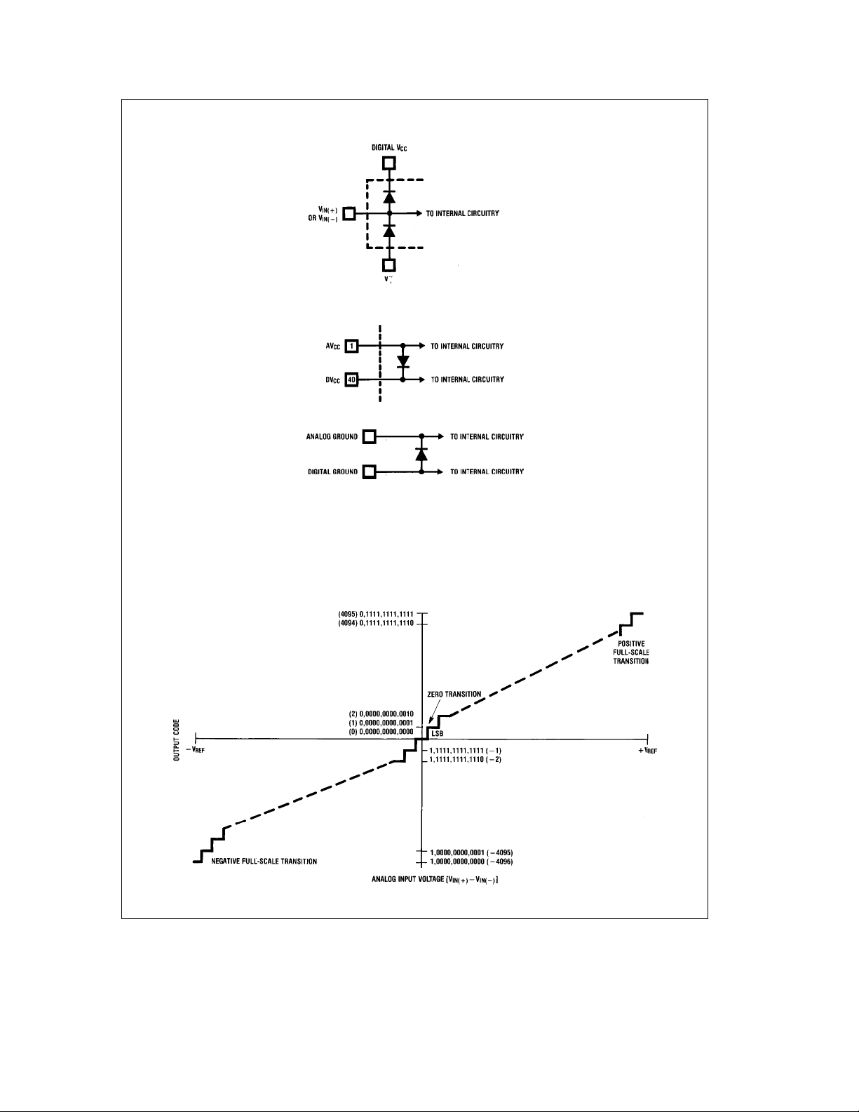
Note 4: Two on-chip diodes are tied to each analog input as shown below.
Errors in the A/D conversion can occur if these diodes are forward biased more than 50 mV. This means that if AVCCand DVCCare minimum (4.75 VDC) and Vbis
b
minimum (
Note 5: A diode exists between analog V
To guarantee accuracy, it is required that the AVCCand DVCCbe connected together to a power supply with separate bypass filters at each VCCpin.
Note 6: A diode exists between analog ground and digital ground.
To guarantee accuracy, it is required that the analog ground and digital ground be connected together externally.
Note 7: Accuracy is guaranteed at f
Note 8: Typicals are at 25
Note 9: Tested and guaranteed to National’s AOQL (Average Outgoing Quality Level).
Note 10: Guaranteed, but not 100% production tested. These limits are not used to calculate outgoing quality levels.
Note 11: Linearity error is defined as the deviation of the analog value, expressed in LSBs, from the straight line which passes through positive full scale and zero,
after adjusting zero error. (See
Note 12: Human body model; 100 pF discharged through a 1.5 kX resistor.
4.75VDC), full-scale must bes4.8VDC.
C and represent most likely parametric norm.
§
Figures 1b
and digital VC.
CC
e
1.0 MHz. At higher clock frequencies accuracy may degrade.
CLK
and1c).
TL/H/5676– 4
TL/H/5676– 20
TL/H/5676– 21
FIGURE 1a. Transfer Characteristic
5
TL/H/5676– 8
Page 6
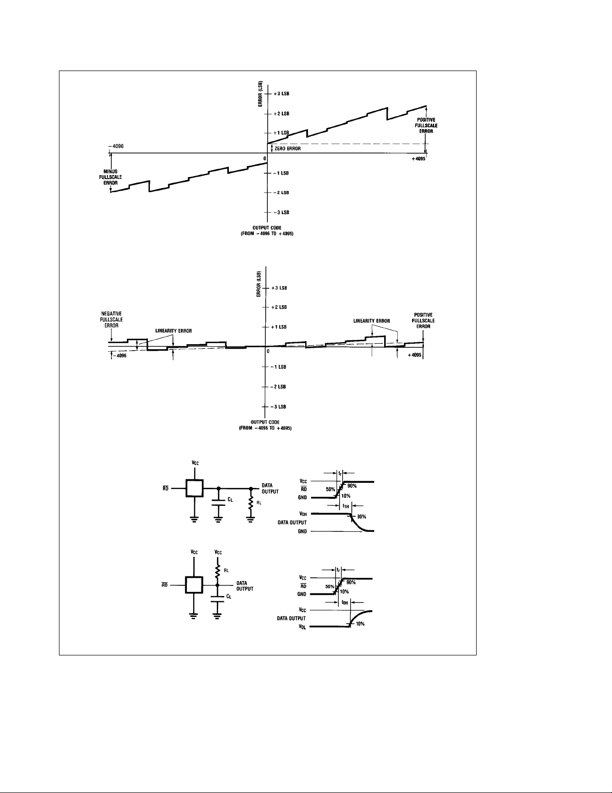
FIGURE 1b. Simplified Error Curve vs. Output Code Without Zero and Fullscale Adjustment
TL/H/5676– 22
FIGURE 1c. Simplified Error Curve vs. Output Code after Zero/Fullscale Adjustment
TL/H/5676– 7
FIGURE 2. TRI-STATE Test Circuits and Waveforms
6
TL/H/5676– 23
Page 7

Timing Diagrams
TL/H/5676– 15
FIGURE 3. Timing Diagram
TL/H/5676– 13
FIGURE 4. Ready Out
FIGURE 5. Data Out
7
TL/H/5676– 14
Page 8

TL/H/5676– 5
FIGURE 6. Functional Block Diagram
8
Page 9

Functional Description
1.0 THE A/D CONVERSION
1.1 STARTING A CONVERSION
When using the ADC1225 or ADC1205 with a microprocessor, starting an A-to-D conversion is like writing to an external memory location. The WR
the conversion. The simplified logic (
the falling edge of WR
flop and initiates the conversion sequence. A new conversion can therefore be restarted before the end of the previous sequence. INT
end.
1.2 THE CONVERSION PROCESS (Numbers designated
by[]refer to portions of
The SARS LOGIC[2]controls the A-to-D conversion process. When ‘sars’ goes high the clock (clk) is gated to the
TIMING GENERATOR[9]. One of the outputs of the TIMING GENERATOR, T
sive Approximation Register, SAR LOGIC[5]. The T
rate is (/8 of the CLK IN frequency.
Inputs to the 12-BIT DAC[11]and control of the SAMPLED
DATA COMPARATOR[10]sign logic are provided by the
SAR LOGIC. The first step in the conversion process is to
set the sign to positive (logic ‘0’) and the input of the DAC to
000 (HEX notation). If the differential input, V
is positive the sign bit will remain low. If it is negative the
sign bit will be set high. Differential inputs of only a few
hundred microvolts are enough to provide full logic swings
at the output of the SAMPLED DATA COMPARATOR.
The sign bit indicates the polarity of the differential input. If it
is set high, the negative input must have been greater than
the positive input. By reversing the polarity of the differential
input, V
sees the negative input as positive. The input polarity rever-
IN(a)
and V
sal is done digitally by changing the timing on the input sampling switches of the SAMPLED DATA COMPARATOR.
Thus, with almost no additional circuitry, the A/D is extended from a unipolar 12-bit to a bipolar 12-bit (12-bit plus sign)
device.
After determining the input polarity, the conversion proceeds with the successive approximation process. The SAR
LOGIC successively tries each bit of the 12-BIT DAC. The
most significant bit (MSB), B11, has a weight of (/2 of V
The next bit, B10, has a weight of (/4 V
bit is reduced in weight by a factor of 2 which gives the least
significant bit (LSB) a weight of 1/4096 V
When the MSB is tried, the comparator compares the DAC
output, V
greater than V
set the MSB. If the analog input is less than V
/2, to the analog input. If the analog input is
REF
/2 the comparator tells the SAR LOGIC to
REF
comparator tells the SAR LOGIC to reset the MSB. On the
next bit-test the DAC output will either be */4 V
V
depending on whether the MSB was set or not. Fol-
REF
lowing this sequence through for each successive bit will
approximate the analog input to within 1-bit (one part in
4096).
On completion of the LSB bit-test the conversion-complete
flip-flop (CC) is set, signifying that the conversion is finished.
The end-of-conversion (EOC) and interrupt (INT
not changed at this time. Some internal housekeeping tasks
must be completed before the outside world is notified that
the conversion is finished.
and CS lines are used to start
Figure 6
) shows that
with CS low clocks the D-type flip-
going low indicates the conversion’s
Figure 6
.)
, provides the clock for the Succes-
z
are interchanged and the DAC
IN(b)
. Each successive
REF
REF
IN(a)
.
b
REF
REF
clock
z
V
IN(b)
REF
/2 the
or (/4
) lines are
Setting CC enables the UPDATE LOGIC[12]. This logic
controls the transfer of data from the SAR LOGIC to the
OUTPUT LATCH[6]and resets the internal logic in preparation for a new conversion. This means that when EOC
goes high, a new conversion can be immediately started
since the internal logic has already been reset. In the same
way, data is transferred to the OUTPUT LATCH prior to issuing an interrupt. This assures that data can be read immediately after INT
goes low.
2.0 READING THE A/D
The ADC 1225 makes all thirteen bits of the conversion
result available in parallel. Taking CS
the TRI-STATE
output buffers. The conversion result is
É
and RD low enables
represented in 2’s complement format.
The ADC1205 makes the conversion result available in two
eight-bit bytes. The output format is 2’s complement with
extended sign. Data is right justified and presented high
byte first. With CS
low and STATUS high, the high byte
(DB12–DB8) will be enabled on the output buffers the first
time RD
goes low. When RD goes low a second time, the
low byte (DB7– DB0) will be enabled. On each read operation, the ‘byst’ flip-flop is toggled so that on successive
reads alternate bytes will be available on the outputs. The
‘byst’ flip-flop is always reset to the high byte at the end of a
conversion. Table 1 below shows the data bit locations on
,
the ADC1205.
The ADC1205’s STATUS
pin makes it possible to read the
conversion status and the state of the ‘byst’ flip-flop. With
RD
, STATUS and CS low, this information appears on the
data bus. The ‘byst’ status appears on pin 18 (DB2/DB10).
A low output on pin 18 indicates that the next data read will
be the high byte. A high output indicates that the next data
read will be the low byte. A high status bit on pin 22 (DB6/
DB12) indicates that the conversion is in progress. A high
output appears on pin 17 (DB1/DB9) when the conversion
is completed and the data has been transferred to the output latch. A high output on pin 16 (DB0/DB8) indicates that
the conversion has been completed and the data is ready to
read. This status bit is reset when a new conversion is initiated, data is read, or status is read. When reading status or a
conversion result, STATUS
least 600 ns before RD
information is not needed, the STATUS
.
wired to V
a
. Table 2 summarizes the meanings of the four
should always change states at
goes low. If the conversion status
status bits.
TABLE I. Data Bit Locations, ADC1205
HIGH BYTE DB12 DB12 DB12 DB12 DB11 DB10 DB9 DB8
LOW BYTE DB7 DB6 DB5 DB4 DB3 DB2 DB1 DB0
TABLE II. Status Bit Locations and Meanings
Status
Location Bit
Status
Bit
Bit
DB6 SARS ‘‘High’’ indicates that
DB2 BYST ‘‘Low’’ indicates that Status write
Meaning Clear Status
the conversion is in
progress
the next data read is or toggle it
the high byte. with data
‘‘High’’ indicates that read
the next data read is
the low byte
pin should be hard-
Condition to
9
Page 10

Functional Description (Continued)
TABLE II. Status Bit Locations and Meanings
Status Status Condition to
Bit Bit Meaning Clear Status
Location Bit
DB1 EOC ‘‘High’’ indicates that
DB0 INT ‘‘High’’ indicates that Data read or
3.0 INTERFACE
3.1 RESET OF INTERRUPT
INT
goes low at the end of the conversion and indicates that
data is transferred to the output latch. By reading data, INT
will be reset to high on the leading edge of the first read (RD
going low). INT is also reset on the leading (falling) edge of
WR
when starting a conversion.
3.2 READY OUT
To simplify the hardware connection to high speed microprocessors, a READY OUT line is provided. This allows the
A-to-D to insert a wait state in the mP’s read cycle. The
equivalent circuit and the timing diagram for READY OUT is
shown in
Figures 7
FIGURE 7. READY OUT Equivalent Circuit
(Continued)
the conversion is
completed and data is
transferred to the
output latch.
it is the end of the status read
conversion and the or status
data is ready to read write
and8.
TL/H/5676– 9
FIGURE 8. READY OUT Timing Diagram
TL/H/5676– 10
3.3 RESETTING THE A/D
All the internal logic can be reset, which will abort any conversion in process and reset the status bits. The reset function is achieved by performing a status write (CS
STATUS
are low).
,WRand
3.4 ADDITIONAL TIMING AND INTERFACE OPTIONS
ADC1225
1. WR
and RD can be tied together with CS low continuously or strobed. The previous conversion’s data will be
available when the WR
and RD are low as shown below.
One drawback is that, since the conversion is started on the
falling edge and the data read on the rising edge of WR
/RD,
the first data access will have erroneous information depending on the power-up state of the internal output latches.
If the WR
INTR
/RD strobe is longer than the conversion time,
will never go low to signal the end of a conversion.
The conversion will be completed and the output latches will
be updated. In this case the READY OUT signal can be
used to sense the end of the conversion since it will go low
when the output latches are being updated.
FIGURE 9
10
TL/H/5676– 24
Page 11

Functional Description (Continued)
FIGURE 10
FIGURE 11
TL/H/5676– 25
TL/H/5676– 26
FIGURE 12
11
TL/H/5676– 27
Page 12

Functional Description (Continued)
TL/H/5676– 28
When using this method of conversion only one strobe is
necessary and the rising edge of WR
/RD can be used to
read the current conversion results. These methods reduce
the throughput time of the conversion since the RD
and WR
cycles are combined.
2. With the standard timing WR pulse width longer than the
conversion time a conversion is completed but the INTR
will
never go low to signal the end of a conversion. The output
latches will be updated and valid information will be available when the RD
cycle is accomplished.
FIGURE 13
TL/H/5676– 29
3. Tying CS
initiate a conversion will also yield valid data. The INTR
and RD low continuously and strobing WR to
will
never go low to signal the end of a conversion and the
digital outputs will always be enabled, so using INTR
strobe the WR
line for a continuous conversion cannot be
done with this part.
A simple stand-alone circuit can be accomplished by driving
WR
with the inverse of the READY OUT signal using a sim-
ple inverter as shown below.
to
FIGURE 14
12
TL/H/5676– 30
Page 13

Functional Description (Continued)
ADC1205
Case 1 would be the only one that would appy to the
ADC1205 since two RD
the 13 bits of information on the 8 bit data bus. Simultaneously strobing WR
icant byte on DB0 – DB7 and start a conversion. Pulsing
WR
/RD low before the end of this conversion will enable
the least significant byte of data on the outputs and restart a
conversion.
4.0 REFERENCE VOLTAGE
The voltage applied to the reference input of the converter
defines the voltage span of the analog inputs (the difference
between V
put codes and 4096 negative output codes exist. The
IN(a)
A-to-D can be used in either ratiometric or absolute reference applications. V
source capable of driving the reference input resistance
(typically 4 kX).
In a ratiometric system, the analog input voltage is proportional to the voltage used for the A/D reference. When this
voltage is the system power supply, the V
tied to V
of the system reference as the analog input and A/D refer-
. This technique relaxes the stability requirement
CC
ence move together maintaining the same output code for a
given input condition.
For absolute accuracy, where the analog input varies between very specific voltage limits, the reference pin can be
biased with a time and temperature stable voltage source.
In general, the magnitude of the reference voltage will require an initial adjustment to null out full-scale errors.
5.0 THE ANALOG INPUTS
5.1 DIFFERENTIAL VOLTAGE INPUTS AND COMMON
MODE REJECTION
The differential inputs of the ADC1225 and ADC1205 actually reduce the effects of common-mode input noise, i.e.,
signals common to both V
most typical). The time interval between sampling the ‘‘
b
and ‘‘
‘‘ input is 4 clock periods. Therefore, a change in the
common-mode voltage during this short time interval may
cause conversion errors. For a sinusoidal common-mode
signal the error would be:
V
ERROR(MAX)
where fCMis the frequency of the common-mode signal,
V
is its peak voltage value and f
PEAK
clock frequency. In most cases V
cant. For a 60 Hz common-mode signal to generate a (/4
LSB error (300 mV) with the converter running at 1 MHz its
peak value would have to be 200mV.
5.2 INPUT CURRENT
Due to the sampling nature of the analog inputs, short duration spikes of current enter the ‘‘
input at the leading clock edges during the actual conversion. These currents decay rapidly and do not cause errors
as the internal comparator is strobed at the end of a clock
period.
5.3 INPUT BYPASS CAPACITORS
Bypass capacitors at the inputs will average the current
spikes mentioned in 5.2 and cause a DC current to flow
strobes are necessary to retrieve
and RD low will enable the most signif-
and V
e
, over which 4096 positive out-
IN(b)
must be connected to a voltage
REF
REF
V
PEAK
and V
IN(a)
(2q fCM)
ERROR
a
inputs (60 Hz is
IN(b)
4
f
CLK
is the converter’s
CLK
will not be signifi-
’’ input and exit the ‘‘b’’
pin can be
a
through the output resistance of the analog signal source.
This charge pumping action is worse for continuous conversions with the V
ous conversions with a 1 MHz clock frequency and the
V
input at 5V, the average input current is approximate-
IN(a)
ly 5 mA. For this reason bypass capacitors should not be
input voltage at full-scale. For continu-
IN(a)
used at the analog inputs for high resistance sources
(R
SOURCE
100 X).
If input bypass capacitors are necessary for noise filtering
and high source resistance is desirable to minimize capacitor
size, the detrimental effects of the voltage drop across this
input resistance, due to the average value of the input current, can be minimized with a full-scale adjustment while the
given source resistance and input bypass capacitor are both
in place. This is effective because the average value of the
input current is a linear function of the differential input voltage.
5.4 INPUT SOURCE RESISTANCE
Large values of source resistance where an input bypass
capacitor is not used, will not cause errors as the input currents settle out prior to the comparison time. If a low pass
filter is required in the system, use a low valued series resis-
s
tor (R
100 X) for a passive RC section or add an op amp
RC active low pass filter. For low source resistance applications, (R
the inputs will prevent pickup due to series lead inductance
SOURCE
s
100 X) a 0.001 mF bypass capacitor at
of a long wire. A 100 X series resistor can be used to isolate
this capacitor – both the R and C are placed outside the
feedback loop – from the output of an op amp, if used.
5.5 NOISE
The leads to the analog inputs should be kept as short as
possible to minimize input noise coupling. Both noise and
undesired digital clock coupling to these inputs can cause
errors. Input filtering can be used to reduce the effects of
these sources, but careful note should be taken of sections
5.3 and 5.4 if this route is taken.
6.0 POWER SUPPLIES
’’
Noise spikes on the V
errors as the comparator will respond to this noise. Low
supply line can cause conversion
CC
inductance tantalum capacitors of 1 mF or greater are recommended for supply bypassing. Separate bypass caps
should be placed close to the DV
unregulated voltage source is available in the system, a sep-
and AVCCpins. If an
CC
arate LM340LAZ-5.0 voltage regulator for the A-to-D’s V
(and other analog circuitry) will greatly reduce digital noise
on the supply line.
7.0 ERRORS AND REFERENCE VOLTAGE
ADJUSTMENTS
7.1 ZERO ADJUST
The zero error of the A/D converter relates to the location
of the first riser of the transfer function and can be measured by grounding the V
magnitude positive voltage to the V
the difference between the actual DC input voltage neces-
input and applying a small
IN(b)
IN(a)
sary to just cause an output digital code transition from all
zeroes to 0,0000,0000,0001 and the ideal (/2 LSB value ((/2
e
LSB
0.61 mV for V
ed as shown in
V
is forced to 0V. The potentiometer is adjusted until
IN(b)
the digital output code changes from all zeroes to
REF
Figure 15
e
5VDC). Zero error can be adjust-
.V
is forced to 0.61 mV, and
IN(a)
0,000,0000,0001.
CC
input. Zero error is
13
Page 14

Functional Description (Continued)
A simpler, although slightly less accurate, approach is to
ground V
output. Error will be well under (/2 LSB if the adjustment is
done so that the potentiometer is ‘‘centered’’ within the
0,000,000 range. A positive voltage at the V
reduce the output code. The adjustment range is
b
30 LSB.
7.2 POSITIVE AND NEGATIVE FULL-SCALE
ADJUSTMENT
Unipolar Inputs
Apply a differential input voltage which is 1.5 LSB below the
desired analog full-scale voltage (V
and V
IN(a)
FIGURE 15. Zero Adjust Circuit
, and adjust for all zeros at the
IN(b)
F
input will
OS
a
4to
TL/H/5676– 11
) and adjust the magni-
Typical Applications
*Input must have some
current return path to
signal ground
tude of the V
ing from 0,1111,1111,1110 to 0,1111,1111,1111.
Bipolar Inputs
Do the same procedure outlined above for the unipolar case
and then change the differential input voltage so that the
digital output code is just changing from 1,0000,0000,0001
to 1,0000,0000,0000. Record the differential input voltage,
V
. the ideal differential input voltage for that transition
X
should be;
b
V
#
Calculate the difference between Vx and the ideal voltage;
e
V
D
Then apply a differential input voltage of;
b
V
X
#
and adjust the magnitude of V
code is just changing from 1,0000,0000,0001 to
1,0000,0000,0000. That will obtain the positive and negative
full-scale transition with symmetrical minimum error.
input so that the output code is just chang-
REF
V
F
a
F
8192
J
V
X
D
2
b#b
J
F
a
V
F
8192
J
so the digital output
REF
TL/H/5676– 12
14
Page 15

Typical Applications (Continued)
Protecting the Input
*VIN(b)e0.15 V
15% of V
s
CC
Diodes are 1N914
CC
s
V
85% of V
XDR
TL/H/5676– 16
Operating with Ratiometric Transducers
CC
TL/H/5676– 17
15
Page 16

Typical Applications (Continued)
Bipolar Input Temperature Converter
a
150 tob55§C with 0.04§C resolution
Note: * resistors are 1% metal film types
Strain Gauge Converter with .025% Resolution and Single Power Supply
Note: 1)* resistors are 1% metal film types
2) LF412 power
a
10V and ground
TL/H/5676– 18
TL/H/5676– 19
16
Page 17

Ordering Information
Temperature Range 0§Cto70§C
Non-Linearity 0.024% ADC1205CCJ-1 ADC1225CCD-1 ADC1205CCJ ADC1225CCD
Package Outline J24A D28D J24A D28D
b
40§Ctoa85§C
Physical Dimensions inches (millimeters)
Ceramic Dual-In Line Package (J)
Order Number ADC1205CCJ-1 or ADC1205CCJ
NS Package Number J24A
17
Page 18

Physical Dimensions inches (millimeters) (Continued)
Ceramic Dual-In-Line Package (D)
Order Number ADC1225CCD-1 or ADC1225CCD
NS Package Number D28D
ADC1205/ADC1225 12-Bit Plus Sign mP Compatible A/D Converters
LIFE SUPPORT POLICY
NATIONAL’S PRODUCTS ARE NOT AUTHORIZED FOR USE AS CRITICAL COMPONENTS IN LIFE SUPPORT
DEVICES OR SYSTEMS WITHOUT THE EXPRESS WRITTEN APPROVAL OF THE PRESIDENT OF NATIONAL
SEMICONDUCTOR CORPORATION. As used herein:
1. Life support devices or systems are devices or 2. A critical component is any component of a life
systems which, (a) are intended for surgical implant support device or system whose failure to perform can
into the body, or (b) support or sustain life, and whose be reasonably expected to cause the failure of the life
failure to perform, when properly used in accordance support device or system, or to affect its safety or
with instructions for use provided in the labeling, can effectiveness.
be reasonably expected to result in a significant injury
to the user.
National Semiconductor National Semiconductor National Semiconductor National Semiconductor
Corporation Europe Hong Kong Ltd. Japan Ltd.
1111 West Bardin Road Fax: (
Arlington, TX 76017 Email: cnjwge@tevm2.nsc.com Ocean Centre, 5 Canton Rd. Fax: 81-043-299-2408
Tel: 1(800) 272-9959 Deutsch Tel: (
Fax: 1(800) 737-7018 English Tel: (
National does not assume any responsibility for use of any circuitry described, no circuit patent licenses are implied and National reserves the right at any time without notice to change said circuitry and specifications.
Fran3ais Tel: (
Italiano Tel: (
a
49) 0-180-530 85 86 13th Floor, Straight Block, Tel: 81-043-299-2309
a
49) 0-180-530 85 85 Tsimshatsui, Kowloon
a
49) 0-180-532 78 32 Hong Kong
a
49) 0-180-532 93 58 Tel: (852) 2737-1600
a
49) 0-180-534 16 80 Fax: (852) 2736-9960
 Loading...