

Page 1
ADC10731/ADC10732/ADC10734/ADC10738
10-Bit Plus Sign Serial I/O A/D Converters with Mux,
Sample/Hold and Reference
General Description
This series of CMOS 10-bit plus sign successive approximation A/D converters features versatile analog input multiplexers, sample/hold and a 2.5V band-gap reference. The 1-, 2-,
4-, or 8-channel multiplexers can be software configured for
single-ended or differential mode of operation.
An input sample/hold is implemented by a capacitive reference ladder and sampled-data comparator. This allows the
analog input to vary during the A/D conversion cycle.
In the differential mode, valid outputs are obtained even
when the negative inputs are greater than the positive because of the 10-bit plus sign output data format.
The serial I/O is configured to comply with the NSC MICROWIRE
face to the COPS
can easily interface with standard shift registers and microprocessors.
™
serial data exchange standard for easy inter-
™
and HPC™families of controllers, and
Features
n 0V to 5V analog input range with single 5V power
supply
n Serial I/O (MICROWIRE compatible)
n 1-, 2-, 4-, or 8-channel differential or single-ended
multiplexer
n Software or hardware power down
n Analog input sample/hold function
n Ratiometric or absolute voltage referencing
n No zero or full scale adjustment required
n No missing codes over temperature
n TTL/CMOS input/output compatible
n Standard DIP and SO packages
Key Specifications
n Resolution 10 bits plus sign
n Single supply 5V
n Power dissipation 37 mW (Max)
n In powerdown mode 18 µW
n Conversion time 5µs (Max)
n Sampling rate 74 kHz (Max)
n Band-gap reference 2.5V
Applications
n Medical instruments
n Portable and remote instrumentation
n Test equipment
May 1999
±
2%(Max)
ADC10731/ADC10732/ADC10734/ADC10738 10-Bit Plus Sign Serial I/O A/D Converters with Mux,
Sample/Hold and Reference
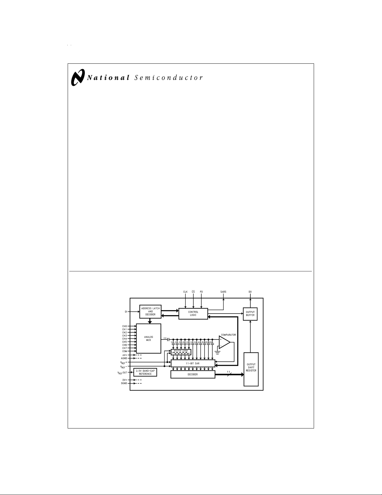
ADC10738 Simplified Block Diagram
DS011390-1
COPS™, HPC™and MICROWIRE™are trademarks of National Semiconductor Corporation.
© 1999 National Semiconductor Corporation DS011390 www.national.com
Page 2
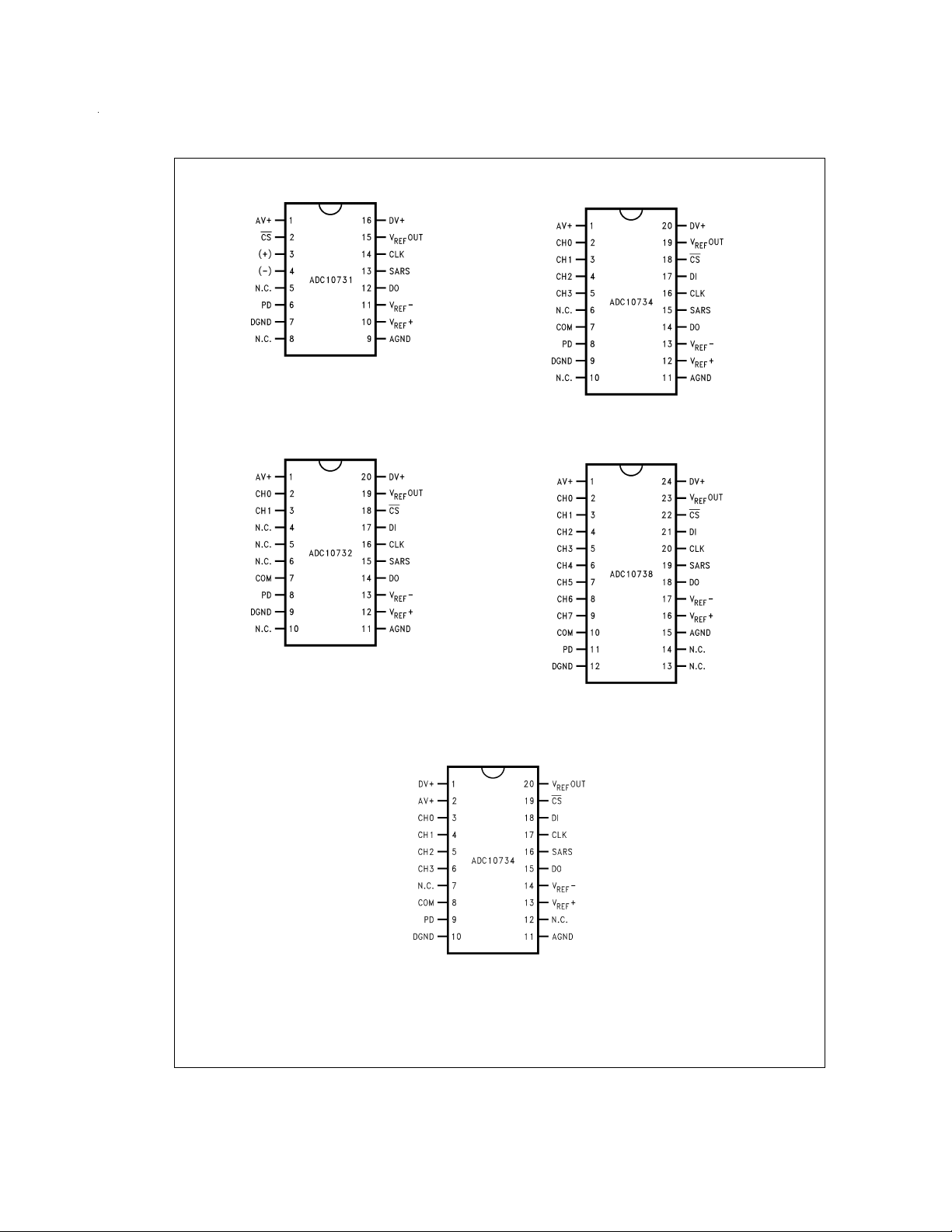
Connection Diagrams
Top View
See NS Package Number M16B
DS011390-2
DS011390-4
Top View
See NS Package Number M20B
DS011390-3
Top View
See NS Package Number M20B
SSOP Package
See NS Package Number MSA20
www.national.com 2
DS011390-5
Top View
See NS Package Number M24B
DS011390-34
Page 3
Ordering Information
Industrial Temperature Range Package
−40˚C ≤ T
≤ +85˚C
A
ADC10731CIWM M16B
ADC10732CIWM M20B
ADC10734CIMSA MSA20
ADC10734CIWM M20B
ADC10738CIWM M24B
Pin Descriptions
CLK The clock applied to this input controls the suc-
DI This is the serial data input pin. The data applied
DO The data output pin. The A/D conversion result
CS
PD This is the power down input pin. When a logic
SARS This is the successive approximation register
CH0–CH7 These are the analog inputs of the MUX. A chan-
COM This pin is another analog input pln. It can be
V
REF
cessive approximation conversion time interval,
the acquisition time and the rate at which the serial data exchange occurs. The rising edge loads
the information on the DI pin into the multiplexer
address shift register. This address controls
which channel of the analog input multiplexer
(MUX) is selected. The falling edge shifts the
data resulting from the A/D conversion out on
DO. CS enables or disables the above functions.
The clock frequency applied to this input can be
between 5 kHz and 3 MHz.
to this pln is shifted by CLK into the multiplexer
address register.
Tables 1, 2, 3
show the multi-
plexer address assignment.
(DB0-SIGN) are clocked out by the failing edge
of CLK on this pin.
This is the chip select input pin. When a logic low
is applied to this pin, the rising edge of CLK
shifts the data on DI into the address register.
This low also brings DO out of TRI-STATE after
a conversion has been completed.
high is applied to this pin the A/D is powered
down. When a low is applied the A/D is powered
up.
status output pin. When CS is high this pin is in
TRI-STATE. With CS low this pin is active high
when a conversion is in progress and active low
at all other times.
nel input is selected by the address information
at the DI pin, which is loaded on the rising edge
of CLK into the address register (see
3
).
The voltage applied to these inputs should not
exceed AV
+
or go below GND by more than
Tables1, 2,
50 mV. Exceeding this range on an unselected
channel will corrupt the reading of a selected
channel.
used as a “pseudo ground” when the analog
multiplexer is single-ended.
+ This is the positive analog voltage reference in-
put. In order to malntaln accuracy, the voltage
range V
REF(VREF
5.0 V
and the voltage at V
DC
+
AV
+50 mV.
=
+–V
V
REF
−) is 0.5 VDCto
REF
+ cannot exceed
REF
V
− The negative voltage reference input. In order to
REF
maintain accuracy, the voltage at this pin must
not go below GND − 50 mV or exceed AV
+50mV.
+
,DV+These are the analog and digital power supply
AV
pins. These pins should be tied to the same
power supply and bypassed separately.The operating voltage range of AV
+
and DV+is 4.5 V
to 5.5 VDC.
DGND This is the digital ground pin.
AGND This is the analog ground pin.
+
DC
www.national.com3
Page 4
Absolute Maximum Ratings (Notes 1, 3)
If Military/Aerospace specified devices are required,
please contact the National Semiconductor Sales Office/
Distributors for availability and specifications.
+
+
Supply Voltage (V
=
AV
Total Reference Voltage
+–V
(V
REF
−) 6.5V
REF
Voltage at Inputs and Outputs V
Input Current at Any Pin (Note 4) 30 mA
Package Input Current (Note 4) 120 mA
Package Dissipation at T
(Note 5) 500 mW
ESD Susceptability (Note 6)
Human Body Model 2500V
Machine Model 150V
Soldering Information
N packages (10 seconds) 260˚C
SO Package (Note 7)
+
=
) 6.5V
DV
=
25˚C
A
+
+ 0.3V to −0.3V
Vapor Phase (60 seconds) 215˚C
Infrared (15 seconds) 220˚C
Storage Temperature −40˚C to +150˚C
Operating Ratings (Notes 2, 3)
Operating Temperature Range T
ADC10731CIWM,
ADC10732CIWM,
ADC10734CIWM,
ADC10734CIMSA,
ADC10738CIWM −40˚C ≤ T
Supply Voltage
+
+
=
AV
(V
+AV
V
REF
−AV
V
REF
V
REF(VREF
+
=
) +4.5V to +5.5V
DV
+–V
−) +0.5V to V
REF
≤ TA≤ T
MIN
+
+50 mV to −50 mV
+
+50 mV to −50 mV
≤ +85˚C
A
MAX
+
Electrical Characteristics
The following specifications apply for V
Characteristics, VIN−=GND for Unsigned Characteristics and f
ply for T
=
=
T
A
to T
T
J
MIN
MAX
+
+
=
AV
; all other limits T
+
=
=
DV
+5.0 V
=
=
T
+25˚C. (Notes 8, 9, 10)
A
J
+=2.5 VDC,V
DC,VREF
=
2.5 MHz unless otherwise specified. Boldface limits ap-
CLK
−=GND, VIN−=2.5V for Signed
REF
Symbol Parameter Conditions Typical Limits Units
(Note 11) (Note 12) (Limits)
SIGNED STATIC CONVERTER CHARACTERISTICS
Resolution with No Missing Codes 10 + Sign Bits
TUE Total Unadjusted Error (Note 13)
INL Positive and Negative Integral
±
2.0 LSB(max)
±
1.25 LSB(max)
Linearity Error
Positive and Negative
±
1.5 LSB(max)
Full-Scale Error
Offset Error
±
1.5 LSB(max)
Power Supply Sensitivity
Offset Error V
+ Full-Scale Error
− Full-Scale Error
DC Common Mode Error (Note 14) V
Multiplexer Channel to
±
10
+5.0V
+=VIN−=VINwhere
IN
5.0V ≥ V
≥ 0V
IN
%
±
0.2
±
0.2
±
0.1
±
0.1
±
0.1 LSB
±
1.0 LSB(max)
±
1.0 LSB(max)
±
0.75 LSB(max)
±
0.33 LSB(max)
+
=
Channel Matching
UNSIGNED STATIC CONVERTER CHARACTERISTICS
Resolution with No Missing Codes 10 Bits
TUE Total Unadjusted Error (Note 13) V
INL Integral Linearity Error V
Full-Scale Error V
Offset Error V
+=4.096V
REF
+=4.096V
REF
+=4.096V
REF
+=4.096V
REF
±
0.75 LSB
±
0.50 LSB
±
1.25 LSB(max)
±
1.25 LSB(max)
Power Supply Sensitivity
+
=
Offset Error V
Full-Scale Error V
DC Common Mode Error (Note 14) V
Multiplexer Channel to Channel
Matching
±
10
+5.0V
+=4.096V
REF
+=VIN−=VINwhere
IN
+5.0V ≥ V
V
REF
≥ 0V
IN
+=4.096V
%
±
0.1 LSB
±
0.1 LSB
±
0.1 LSB
±
0.1 LSB
www.national.com 4
Page 5
Electrical Characteristics (Continued)
+
+
The following specifications apply for V
Characteristics, VIN−=GND for Unsigned Characteristics and f
ply for T
=
=
T
A
to T
T
J
MIN
MAX
=
AV
; all other limits T
Symbol Parameter Conditions Typical Limits Units
DYNAMIC SIGNED CONVERTER CHARACTERISTICS
S/(N+D) Signal-to-Noise Plus Distortion Ratio V
ENOB Effective Number of Bits V
THD Total Harmonic Distortion V
IMD Intermodulation Distortion V
Full-Power Bandwidth V
Multiplexer Channel to Channel
Crosstalk
DYNAMIC UNSIGNED CONVERTER CHARACTERISTIC
S/(N+D) Signal-to-Noise Plus Distortion Ratio V
Effective Bits V
THD Total Harmonic Distortion V
IMD Intermodulation Distortion V
Full-Power Bandwidth V
Multiplexer Channel to Channel f
Crosstalk V
REFERENCE INPUT AND MULTIPLEXER CHARACTERISTICS
Reference Input Resistance 7 kΩ
C
REF
Reference Input Capacitance 70 pF
MUX Input Voltage −50 mV(min)
C
IM
MUX Input Capacitance 47 pF
Off Channel Leakage Current
(Note 15)
On Channel Leakage Current On Channel=5V and 0.4 3.0 µA(max)
+
=
=
DV
+5.0 V
=
=
T
+25˚C. (Notes 8, 9, 10)
A
J
+=2.5 VDC,V
DC,VREF
=
2.5 MHz unless otherwise specified. Boldface limits ap-
CLK
−=GND, VIN−=2.5V for Signed
REF
(Note 11) (Note 12) (Limits)
IN
and f
IN
and f
IN
and f
IN
and f
IN
=
IN
=
IN
=
IN
=
IN
=
,67 dB
4.85 V
PP
=
1 kHz to 15 kHz
, 10.8 Bits
4.85 V
PP
=
1 kHz to 15 kHz
, −78 dB
4.85 V
PP
=
1 kHz to 15 kHz
, −85 dB
4.85 V
PP
=
1 kHz to 15 kHz
, where 380 kHz
4.85 V
PP
S/(N + D) Decreases
3dB
=
f
15 kHz −80 dB
IN
+=4.096V,
REF
=
V
IN
=
f
IN
REF
=
V
IN
=
f
IN
REF
=
V
IN
=
f
IN
REF
=
V
IN
=
f
IN
=
IN
V
REF
, and 60 dB
4.0 V
PP
1 kHz to 15 kHz
+=4.096V,
, and 9.8 Bits
4.0 V
PP
1 kHz to 15 kHz
+=4.096V,
, and −70 dB
4.0 V
PP
1 kHz to 15 kHz
+=4.096V,
, and −73 dB
4.0 V
PP
1 kHz to 15 kHz
,
4.0 V
PP
+=4.096V, 380 kHz
where S/(N+D) decreases
3dB
=
15 kHz,
IN
REF
+=4.096V
−80 dB
5.0 kΩ(min)
9.5 kΩ(max)
+
AV
+50 mV (max)
On Channel=5V and −0.4 −3.0 µA(max)
Off Channel=0V
On Channel=0V and 0.4 3.0 µA(max)
Off Channel=5V
www.national.com5
Page 6
Electrical Characteristics (Continued)
+
+
The following specifications apply for V
Characteristics, VIN−=GND for Unsigned Characteristics and f
ply for T
=
=
T
A
to T
T
J
MIN
MAX
=
AV
; all other limits T
Symbol Parameter Conditions Typical Limits Units
REFERENCE INPUT AND MULTIPLEXER CHARACTERISTICS
(Note 15) Off Channel=0V
REFERENCE CHARACTERISTICS
V
Out Reference Output Voltage 2.5V±0.5
REF
∆V
/∆TV
REF
∆V
/∆ILLoad Regulation, Sourcing 0 mA ≤ IL≤ +4 mA
REF
∆V
/∆ILLoad Regulation, Sinking 0 mA ≤ IL≤ −1 mA
REF
Out Temperature Coefficient
REF
Line Regulation 5V
I
SC
Short Circuit Current V
Noise Voltage
∆V
/∆t Long-term Stability
REF
t
SU
Start-Up Time C
DIGITAL AND DC CHARACTERISTICS
V
IN(1)
V
IN(0)
I
IN(1)
I
IN(0)
V
OUT(1)
V
OUT(0)
I
OUT
+I
SC
−I
SC
I
+ Digital Supply Current CS=HIGH, Power Up 0.9 1.3 mA(max)
D
Logical “1” Input Voltage V
Logical “0” Input Voltage V
Logical “1” Input Current V
Logical “0” Input Current V
Logical “1” Output Voltage V
Logical “0” Output Voltage V
TRI-STATE Output Current V
Output Short Circuit Source Current V
Output Short Circuit Sink Current V
(Note 17) CS=HIGH, Power Down
I
+ Analog Supply Current CS=HIGH, Power Up 2.7 6.0 mA(max)
A
(Note 17) CS=HIGH, Power Down
I
REF
Reference Input Current V
AC CHARACTERISTICS
f
CLK
Clock Frequency 3.0 2.5 MHz(max)
Clock Duty Cycle 40
t
C
t
A
Conversion Time 12 12 Clock
Acquisition Time 4.5 4.5 Clock
+
=
=
DV
+5.0 V
=
=
T
+25˚C. (Notes 8, 9, 10)
A
J
+=2.5 VDC,V
DC,VREF
=
2.5 MHz unless otherwise specified. Boldface limits ap-
CLK
−=GND, VIN−=2.5V for Signed
REF
(Note 11) (Note 12) (Limits)
On Channel=0V and −0.4 −3.0 µA(max)
Off Channel=5V
%
±
40 ppm/˚C
±
0.003
±
0.2
±
%
10
Out=0V 13 22 mA(max)
REF
10 Hz to 10 kHz,
=
100 µF
C
L
=
100 µF 100 ms
L
+
=
5.5V 2.0 V(min)
+
=
4.5V 0.8 V(max)
=
5.0V 0.005 +2.5 µA(max)
IN
=
0V −0.005 −2.5 µA(max)
IN
+
=
4.5V, I
+
=
V
4.5V, I
+
=
4.5V, I
=
OUT
=
V
OUT
=
OUT
=
OUT
=
−360 µA 2.4 V(min)
OUT
=
−10 µA 4.5 V(min)
OUT
=
1.6 mA 0.4 V(min)
OUT
0V −0.1 −3.0 µA(max)
5V +0.1 +3.0 µA(max)
+
=
0V, V
V
4.5V −30 −15 mA(min)
+
=
4.5V 30 15 mA(min)
±
0.3
5µV
±
120 ppm/kHr
%
2.5V±2
±
0.05
±
0.6
±
2.5 mV(max)
0.2 0.4 mA(max)
CS=HIGH, Power Down,
0.5 50 µA(max)
and CLK Off
3 15 µA(max)
+=+2.5V and 0.6 mA(max)
REF
CS=HIGH, Power Up
5 kHz(min)
60
5 5 µs(max)
2 2 µs(max)
V(max)
%
/mA(max)
%
/mA(max)
%
(min)
%
(max)
Cycles
Cycles
www.national.com 6
Page 7
Electrical Characteristics (Continued)
+
+
The following specifications apply for V
Characteristics, VIN−=GND for Unsigned Characteristics and f
ply for T
=
=
T
A
to T
T
J
MIN
MAX
=
AV
; all other limits T
Symbol Parameter Conditions Typical Limits Units
AC CHARACTERISTICS
t
SCS
CS Set-Up Time, Set-Up Time from
Falling Edge of CS to Rising Edge of
Clock
DI Set-Up Time, Set-Up Time from
t
SDI
Data Valid on DI to Rising Edge of
Clock
DI Hold Time, Hold Time of DI Data
t
HDI
from Rising Edge of Clock to Data
not Valid on DI
DO Access Time from Rising Edge of
t
AT
CLK When CS is “Low” during a
Conversion
DO or SARS Access Time from CS ,
t
AC
Delay from Falling Edge of CS to
Data Valid on DO or SARS
Delay from Rising Edge of Clock to
t
DSARS
t
HDO
Falling Edge of SARS when CS is
“Low”
DO Hold Time, Hold Time of Data on
DO after Falling Edge of Clock
DO Access Time from Clock, Delay
t
AD
t
1H,t0H
t
DCS
t
CS(H)
t
CS(L)
t
SC
t
PD
t
PC
C
IN
C
OUT
Note 1: Absolute Maximum Ratings indicate limits beyond which damage to the device may occur.
Note 2: Operating Ratings indicate conditions for which the device is functional, but do not guarantee specific performance limits. For guaranteed specifcations and
test conditions, see the Electrical Characteristics. The guaranteed specifications apply only for the test conditions listed. Some performance characteristics may degrade when the device is not operated under the listed test conditions.
Note 3: All voltages are measured with respect to GND, unless otherwise specified.
Note 4: When the input voltage (V
The 120 mA maximum package input current rating limits the number of pins that can safely exceed the power supplies with an input current of 30 mA to four.
Note 5: The maximum power dissipation must be derated at elevated temperatures and is dictated by T
allowable power dissipation at any temperature is P
T
from Falling Edge of Clock to Valid
Data of DO
Delay from Rising Edge of CS to DO
or SARS TRI-STATE
Delay from Falling Edge of Clock to
Falling Edge of CS
CS “HIGH” Time for A/D Reset after
Reading of Conversion Result
ADC10731 Minimum CS “Low” Time
to Start a Conversion
Time from End of Conversion to CS
Going “Low”
Delay from Power-Down command to
10%of Operating Current
Delay from Power-Up Command to
Ready to Start a New Conversion
Capacitance of Logic Inputs 7 pF
Capacitance of Logic Outputs 12 pF
) at any pin exceeds the power supplies (V
IN
=
(T
=
150˚C. The typical thermal resistance (θ
Jmax
D
) of these Paris when board mounted can be found in the following table:
JA
+
=
=
DV
+5.0 V
=
=
T
+25˚C. (Notes 8, 9, 10)
A
J
+=2.5 VDC,V
DC,VREF
=
2.5 MHz unless otherwise specified. Boldface limits ap-
CLK
−=GND, VIN−=2.5V for Signed
REF
(Note 11) (Note 12) (Limits)
14 30 ns(min)
(1 t
CLK
(1 t
CLK
−14ns) −30 ns)
16 25 ns(min)
2 25 ns(min)
30 50 ns(min)
30 70 ns(max)
100 200 ns(max)
20 35 ns(max)
40 80 ns(max)
40 50 ns(max)
20 30 ns(min)
1 CLK 1 CLK cycle(min)
1 CLK 1 CLK cycle(min)
5 CLK 5 CLK
1µs
10
<
GND or V
IN
)/θJAor the number given In the Absolute Maximum Ratings, whichever is lower. For this device,
Jmax−TA
>
AV+or DV+), the current at that pln should be limited to 30 mA.
IN
, θJAand the ambient temperature, TA. The maximum
Jmax
(max)
cycle(min)
µs
www.national.com7
Page 8
Electrical Characteristics (Continued)
Part Number Thermal Resistance Package
Type
ADC10731CIWM 90˚C/W M16B
ADC10732CIWM 80˚C/W M20B
ADC10734CIMSA 134˚C/W MSA20
ADC10734CIWM 80˚C/W M20B
ADC10738CIWM 75˚C/W M24B
Note 6: The human body model is a 100 pF capacitor discharged through a 1.5 kΩ resistor into each pin. The machine model is a 200 pF capacitor discharged di-
rectly into each pin.
Note 7: SeeAN-450 “Surface Mounting Methods and Their Effect on Product Reliability” or the section titied “Surtace Mount” found in any post 1986 National Semiconductor Linear Data Book for other methods of soldering surtace mount devices.
Note 8: Twoon-ohip diodes are tied to each analog input as shown below. They will forward-conduct for analog input voltages one diode drop below ground or one
diode drop greater than V
at elevated temperatures, which will cause errors In the conversion result. The specification allows 50 mV forward bias of either diode; this means that as long as
the analog V
the reading of a selected channel. If AV
Note 9: No connection exists between AV
To guarantee accuracy, it is required that the AV
Note 10: One LSB is referenced to 10 bits of resolution.
Note 11: Typicals are at T
Note 12: Tested limits are guaranteed to National’s AOQL (Average Outgolng Quality Level).
Note 13: Total unadjusted error includes offset, full-scale, linearity, multiplexer, and hold step errors.
Note 14: The DC common-mode error is measured in the differential multiplexer mode with the assigned positive and negative input channels shorted together.
Note 15: Channel leakage current is measured after the channel selection.
Note 16: All the timing specifications are tested at the TTL logic levels, V
to 1.4V.
Note 17: The voltage applied to the digital inputs will affect the current drain during power down. These devices are tested with CMOS logic levels (logic Low=0V
and logic High=5V). TTL levels increase the current, during power down, to about 300 µA.
IN
+
supply.Becareful during testing at low V+levels (+4.5V), as high level analog inputs (+5V) can cause an input diode to conduct, especially
does not exceed the supply voltage by more than 50 mV, the output code will be oorrect. Exceeding this range on an unselected channel will corrupt
J
+
and DV+are minimum (4.5 VDC) and full scale must be ≤+4.55 VDC.
+
and DV+on the chip.
+
and DV+be connected together to a power supply with separate bypass filter at eacn V+pin.
=
=
T
25˚C and represent most likely pararmetric norm.
A
=
0.8V for a falling edge and V
IL
DS011390-6
=
2.0V for a rising. TRl-STATE voltage level is forced
IH
www.national.com 8
Page 9
Electrical Characteristics (Continued)
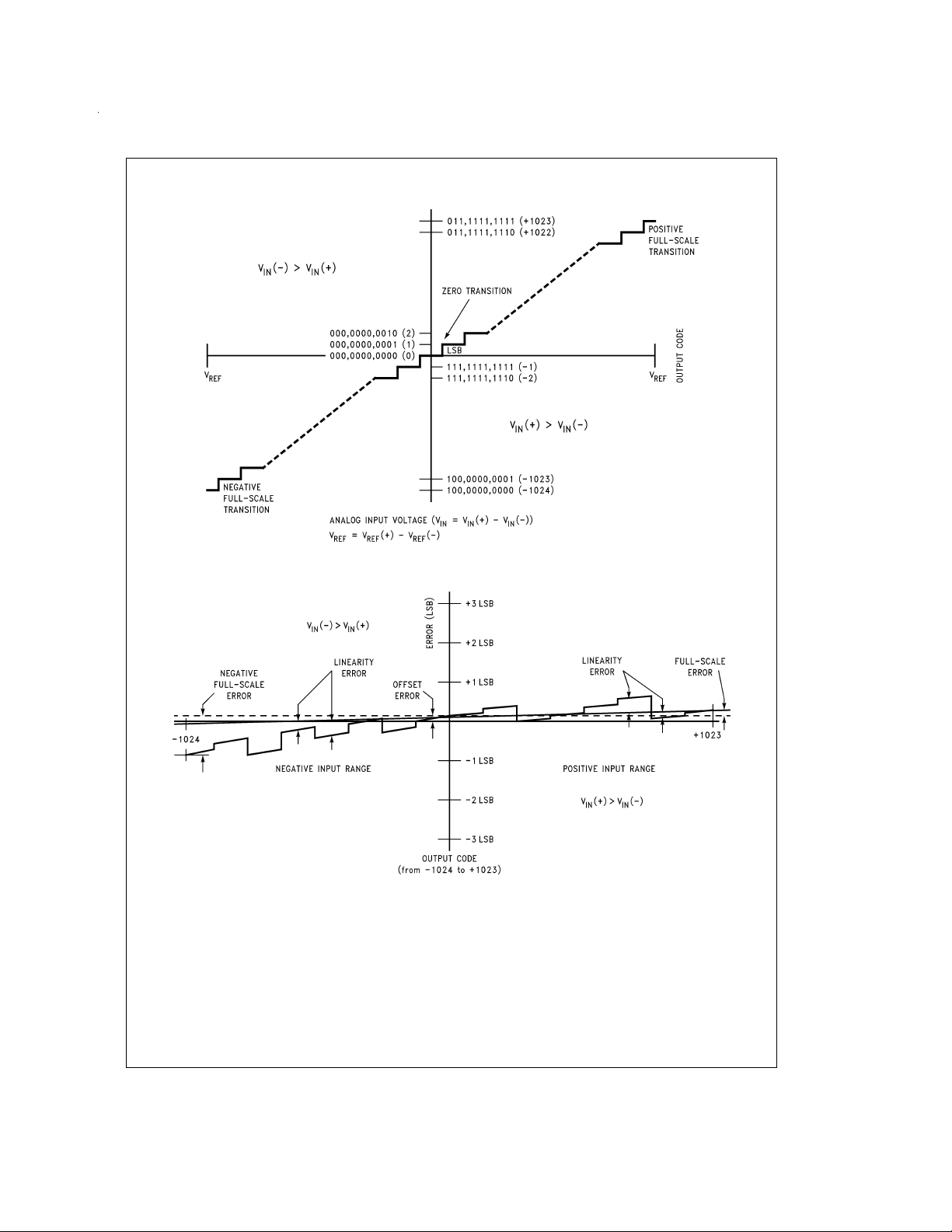
FIGURE 1. Transter Characteristic
DS011390-8
FIGURE 2. Simplified Error Curve vs Output Code
DS011390-26
www.national.com9
Page 10

Electrical Characteristics (Continued)
Leakage Current Test Circuit
Typical Performance Characteristics
DS011390-9
Analog Supply Current (IA+)
vs Temperature
Digital Supply Current (ID+)
vs Clock Frequency
DS011390-35
DS011390-38
Analog Supply Current (IA+)
vs Clock Frequency
Offset Error
vs Reference Voltage
DS011390-39
DS011390-36
Digital Supply Current (ID+)
vs Temperature
DS011390-37
Offset Error
vs Temperature
DS011390-40
www.national.com 10
Page 11

Typical Performance Characteristics (Continued)
Linearity Error
vs Clock Frequency
10-Bit Unsigned
Signal-to-Noise + THD Ratio
vs Input Signal Level
DS011390-44
DS011390-41
Linearity Error
vs Reference Voltage
Spectral Response with
34 kHz Sine Wave
DS011390-42
DS011390-45
Linearity Error
vs Temperature
DS011390-43
Power Bandwidth Response
with 380 kHz Sine Wave
DS011390-46
Typical Reference Performance Characteristics
Load Regulation
DS011390-47
Line Regulation
DS011390-48
Output Drift
vs Temperature
(3 Typical Parts)
DS011390-49
www.national.com11
Page 12

Typical Reference Performance Characteristics (Continued)
Available
Output Current
vs Supply Voltage
DS011390-50
TRI-STATE Test Circuits and Waveforms
Timing Diagrams
DS011390-10
DS011390-12
DS011390-11
DS011390-13
DS011390-14
FIGURE 3. DI Timing
www.national.com 12
Page 13

Timing Diagrams (Continued)
DS011390-15
FIGURE 4. DO Timing
FIGURE 5. Delayed DO Timing
FIGURE 6. Hardware Power Up/Down Sequence
DS011390-16
DS011390-17
www.national.com13
Page 14

Timing Diagrams (Continued)
FIGURE 7. Software Power Up/Down Sequence
DS011390-18
Note: If CS is low during power up of the power supply voltages (AV+and DV+) then CS needs to go high for t
is invalid.
FIGURE 8. ADC10731 CS Low during Conversion
www.national.com 14
. The data output after the first conversion
CS(H)
DS011390-19
Page 15

Timing Diagrams (Continued)
DS011390-20
. The data output after the first conversion
CS(H)
) then CS needs to go high for t
+
and DV
+
Note: If CS is low during power up of the power supply voltages (AV
is not valid.
FIGURE 9. ADC10732, ADC10734 and ADC10738 CS Low during Conversion
www.national.com15
Page 16

Timing Diagrams (Continued)
DS011390-21
. The data output after the first conversion
CS(H)
www.national.com 16
) then CS needs to go high for t
+
and DV
+
Note: If CS is low during power up of the power supply voltages (AV
is not valid.
FIGURE 10. ADC10731 Using CS to Delay Output of Data afer a Conversion has Completed
Page 17

Timing Diagrams (Continued)
DS011390-22
. The data output after the first conversion
CS(H)
) then CS needs to go high for t
+
and DV
+
Note: If CS is low during power up of the power supply voltages (AV
is not valid.
FIGURE 11. ADC10732, ADC10734 and ADC10738 Using CS to Delay Output of Data after a Conversion has Completed
www.national.com17
Page 18

Timing Diagrams (Continued)
TABLE 1. ADC10738 Multiplexer Address Assignment
MUX Address Channel Number MUX
MA0 MA1 MA2 MA3 MA4 CH0 CH1 CH2 CH3 CH4 CH5 CH6 CH7 COM
PU SING/ ODD/ SEL1 SEL0
DIFF SIGN
11000+ −
11001 + −
11010 + −
1 1 0 1 1 + − Single-Ended
11100 + −
11101 + −
11110 + −
11111 +−
10000+−
10001 +−
10010 +−
1 0 0 1 1 + − Differential
10100−+
10101 −+
10110 −+
10111 −+
0 X X X X Power Down (All Channels Disconnected)
TABLE 2. ADC10734 Multiplexer Address Assignment
MUX Address Channel Number MUX
MA0 MA1 MA2 MA3 MA4 CH0 CH1 CH2 CH3 COM
PU SING/ ODD/ SEL1 SEL0
DIFF SIGN
11000+ −
1 1 0 0 1 + − Single-Ended
11100 + −
11101 +−
10000+−
1 0 0 0 1 + − Differential
10100−+
10101 −+
0 X X X X Power Down (All Channels Disconnected)
MODE
MODE
TABLE 3. ADC10732 Multiplexer Address Assignment
MUX Address Channel Number MUX
MA0 MA1 MA2 MA3 MA4 CH0 CH1 COM
PU SlNG/DIFF ODD/SIGN SEL1 SEL0
1 1 0 0 0 + − Single-Ended
11100 +−
1 0 0 0 0 + − Differential
10100−+
0 X X X X Power Down (All Channels Disconnected)
www.national.com 18
MODE
Page 19

Applications Hints
The ADC10731/2/4/8 use successive approximation to digitize an analog input voltage. The DAC portion of theA/D converters uses a capacitive array and a resistive ladder structure. The structure of the DAC allows a very simple switching
scheme to provide a versatile analog input multiplexer. This
structure also provides a sample/hold. The ADC10731/2/4/8
have a 2.5V CMOS bandgap reference. The serial digital I/O
interfaces to MICROWIRE and MICROWIRE+.
1.0 DIGITAL INTERFACE
There are two modes of operation. The fastest throughput
rate is obtained when CS is kept low during a conversion.
The timing diagrams in
the devices in this mode. CS must be taken high for at least
t
(1 CLK) between conversions. This is necessary to re-
CS(H)
set the internal logic.
the devices when CS is taken high while the ADC10731/2/
4/8 is converting. CS may be taken high during the conversion and kept high indefinitely to delay the output data. This
mode simplifies the interface to other devices while the
ADC10731/2/4/8 is busy converting.
1.1 Getting Started with a Conversion
The ADC10731/2/4/8 need to be initialized after the power
supply voltage is applied. If CS is low when the supply voltage is applied then CS needs to be taken high for at least
t
(1 clock period). The data output after the first conver-
CS(H)
sion is not valid.
1.2 Software and Hardware Power Up/Down
These devices have the capability of software or hardware
power down.
Figures 6, 7
ware and software power up/down. In the case of hardware
power down note that CS needs to be high for t
is taken low. When PD is high the device is powered down.
The total quiescent current, when powered down, is typically
200 µA with the clock at 2.5 MHz and 3 µA with the clock off.
The actual voltage level applied to a digital input will effect
the power consumption of the device during power down.
Figures 8, 9
Figures 10, 11
show the operation of
show the operation of
show the timing diagrams for hard-
PC
after PD
CMOS logic levels will give the least amount of current drain
(3 µA). TTL logic levels will increase the total current drain to
200 µA.
These devices have resistive reference ladders which draw
600 µA with a 2.5V reference voltage. The internal band gap
reference voltage shuts down when power down is activated. If an external reference voltage is used, it will have to
be shut down to minimize the total current drain of the device.
2.0 ARCHITECTURE
Before a conversion is started, during the analog input sampling period, (t
the comparator is being zeroed the channel assigned to be
), the sampled data comparator is zeroed. As
A
the positive input is connected to the A/D’s input capacitor.
(The assignment procedure is explained in the Pin Descriptions section.) This charges the input 32C capacitor of the
DAC to the positive analog input voltage. The switches
shown in the DAC portion of
Figure 12
are set for this
zeroing/acquisition period. The voltage at the input and output of the comparator are at equilibrium at this time. When
the conversion is started, the comparator feedback switches
are opened and the 32C input capacitor is then switched to
the assigned negative input voltage. When the comparator
feedback switch opens, a fixed amount of charge is trapped
on the common plates of the capacitors. The voltage at the
input of the comparator moves away from equilibrium when
the 32C capacitor is switched to the assigned negative input
voltage, causing the output of the comparator to go high (“1”)
or low (“0”). The SAR next goes through an algorithm, controlled by the output state of the comparator, that redistributes the charge on the capacitor array by switching the voltage on one side of the capacitors in the array.The objective
of the SAR algorithm is to return the voltage at the input of
the comparator as close as possible to equilibrium.
The switch position information at the completion of the successive approximation routine is a direct representation of
the digital output. This data is then available to be shifted on
the DO pin.
www.national.com19
Page 20

Applications Hints (Continued)
DS011390-28
www.national.com 20
FIGURE 12. Detailed Diagram of the ADC10738 DAC and Analog Multiplexer Stages
Page 21

Applications Hints (Continued)
3.0 APPLICATIONS INFORMATION
3.1 Multiplexer Configuration
The design of these converters utilizes a sampled-data comparator structure, which allows a differential analog input to
be converted by the successive approximation routine.
The actual voltage converted is always the difference between an assigned “+” input terminal and a “−” input terminal.
The polarity of each input terminal or pair of input terminals
being converted indicates which line the converter expects
to be the most positive.
A unique input multiplexing scheme has been utilized to provide multiple analog channels. The input channels can be
software configured into three modes: differential,
single-ended, or pseudo-differential.
three modes using the 4-channel MUX of the ADC10734.
The eight inputs of the ADC10738 can also be configured in
any of the three modes. The single-ended mode has
CH0–CH3 assigned as the positive input with COM serving
as the negative input. In the differential mode, the
ADC10734 channel inputs are grouped in pairs, CH0 with
CH1 and CH2 with CH3. The polarity assignment of each
channel in the pair is interchangeable. Finally, in the
pseudo-differential mode CH0–CH3 are positive inputs referred to COM which is now a pseudo-ground. This
pseudo-ground input can be set to any potential within the input common-mode range of the converter. The analog signal
conditioning required in transducer-based data acquisition
systems is significantly simplified with this type of input flexibility. One converter package can now handle
ground-referred inputs and true differential inputs as well as
signals referred to a specific voltage.
The analog input voltages for each channel can range from
50 mV below GND to 50 mV above V
degrading conversion accuracy. If the voltage on an unselected channel exceeds these limits it may corrupt the reading of the selected channel.
3.2 Reference Considerations
The voltage difference between the V
defines the analog input voltage span (the difference between V
1024 negative possible output codes apply.
The value of the voltage on the V
anywhere between AV
V
used in either ratiometric applications or in systems requiring
(Max) and VIN(Min)) over which 1023 positive and
IN
+
+
is greater than V
REF
+ 50 mV and −50 mV, so long as
REF
absolute accuracy.The reference pins must be connected to
a voltage source capable of driving the minimum reference
input resistance of 5 kΩ.
The internal 2.5V bandgap reference in the ADC10731/2/4/8
is available as an output on the VREFOut pin. To ensure optimum performance this output needs to be bypassed to
ground with 100 µF aluminum electrolytic or tantalum capacitor.The reference output can be unstable with capacitive
loads greater than 100 pF and less than 100 µF.Any capacitive loading less than 100 pF and greater than 100 µF will not
cause oscillation. Lower output noise can be obtained by increasing the output capacitance.A 100 µF capacitor will yield
a typical noise floor of
Figure 13
+
REF
−
. The ADC10731/2/4/8 can be
+
REF
or V
=
DV
+
and V
REF
illustrates the
+
+
=
without
AV
−
REF
−
inputs can be
inputs
The pseudo-differential and differential multiplexer modes allow for more flexibility in the analog input voltage range since
the “zero” reference voltage is set by the actual voltage applied to the assigned negative input pin.
In a ratiometric system (
Figure 14
), the analog input voltage
is proportional to the voltage used for the A/D reference. This
voltage may also be the system power supply,so V
also be tied to AV
+
. This technique relaxes the stability re-
REF
+ can
quirements of the system reference as the analog input and
A/D reference move together maintaining the same output
code for a given input condition.
For absolute accuracy (
Figure 15
), where the analog input
varies between very specific voltage limits, the reference pin
can be biased with a time- and temperature-stable voltage
source that has excellent initial accuracy. The LM4040,
LM4041 and LM185 references are suitable for use with the
ADC10731/2/4/8.
The minimum value of V
quite small (see Typical Performance Characteristics) to al-
REF(VREF
=
+–V
REF
−) can be
V
REF
low direct conversion of transducer outputs providing less
than a 5V output span. Particular care must be taken with regard to noise pickup, circuit layout and system error voltage
sources when operating with a reduced span due to the increased sensitivity of the converter (1 LSB equals V
1024).
REF
3.3 The Analog Inputs
Due to the sampling nature of the analog inputs, at the clock
edges short duration spikes of current will be seen on the selected assigned negative input. Input bypass capacitors
should not be used if the source resistance is greater than
1kΩsince they will average the AC current and cause an ef-
fective DC current to flow through the analog input source resistance. An op amp RC active lowpass filter can provide
both impedance buffering and noise filtering should a high
impedance signal source be required. Bypass capacitors
may be used when the source impedance is very low without
any degradation in performance.
In a true differential input stage, a signal that is common to
both “+” and “−” inputs is canceled. For theADC10731/2/4/8,
the positive input of a selected channel pair is only sampled
once before the start of a conversion during the acquisition
time (t
). The negative input needs to be stable during the
A
complete conversion sequence because it is sampled before
each decision in the SAR sequence. Therefore, any AC
common-mode signal present on the analog inputs will not
be completely canceled and will cause some conversion errors. For a sinusoid common-mode signal this error is:
V
(max)=V
ERROR
where f
V
PEAK
sion time (t
common-mode signal to generate a
is the frequency of the common-mode signal,
CM
is its peak voltage value, and tCis the A/D’s conver-
C
PEAK
=
12/f
(2 π fCM)(tC)
). For example, for a 60 Hz
CLK
1
⁄4LSB error (0.61 mV)
with a 4.8 µs conversion time, its peak value would have to
be approximately 337 mV.
.
/
www.national.com21
Page 22

Applications Hints (Continued)
4 Single-Ended
DS011390-51
2 Differential
DS011390-52
2 Single-Ended
and 1 Differential
DS011390-54
FIGURE 13. Analog Input Multiplexer Options
Ratiometric Using the Internal Reference
4 Psuedo-
Differential
DS011390-53
FIGURE 14.
www.national.com 22
DS011390-29
Page 23

Applications Hints (Continued)
Absolute Using a 4.096V Span
FIGURE 15. Different Reference Configurations
3.4 Optional Adjustments
3.4.1 Zero Error
The zero error of the A/D converter relates to the location of
the first riser of the transfer function (see
can be measured by grounding the minus input and applying
a small magnitude voltage to the plus input. Zero error is the
difference between actual DC input voltage which is necessary to just cause an output digital code transition from 000
0000 0000 to 000 0000 0001 and the ideal
LSB=1.22 mV for V
REF
=
+ 2.500V).
The zero error of the A/D does not require adjustment. If the
minimum analog input voltage value, V
the effective “zero” voltage can be adjusted to a convenient
value. The converter can be made to output an all zeros digital code for this minimum input voltage by biasing any minus
input to V
pseudo-differential input channel configurations.
(Min). This is useful for either the differential or
IN
3.4.2 Full-Scale
The full-scale adjustment can be made by applying a differential input voltage which is 1
analog full-scale voltage range and then adjusting the V
voltage (V
changing from 011 1111 1110 to 011 1111 1111. In bipolar
REF
=
V
REF
1
⁄2LSB down from the desired
+
−
–V
) for a digital output code
REF
signed operation this only adjusts the positive full scale error.
3.4.3 Adjusting for an Arbitrary Analog Input
Voltage Range
If the analog zero voltage of the A/D is shifted away from
ground (for example, to accommodate an analog input signal
which does not go to ground), this new zero reference
should be properly adjusted first. A plus input voltage which
equals this desired zero reference plus
selected plus input and the zero reference voltage at the corresponding minus input should then be adjusted to just obtain the 000 0000 0000 to 000 0000 0001 code transition.
The full-scale adjustment should be made [with the proper
minus input voltage applied] by forcing a voltage to the plus
input which is given by:
Figures 1, 2
1
⁄2LSB value (1⁄
(Min), is not ground,
IN
1
⁄2LSB is applied to
) and
REF
DS011390-30
where V
V
MIN
range. Both V
(V
REF
a code change from 011 1111 1110 to 011 1111 1111. Note,
when using a pseudo-differential or differential multiplexer
2
mode where V
GND range, the individual values of V
matter, only the difference sets the analog input voltage
equals the high end of the analog input range,
MAX
equals the low end (the offset zero) of the analog
=
V
REF
+
MAX
REF
and V
−V
+ and V
are ground referred. The V
MIN
−
) voltage is then adjusted to provide
REF
− are placed within the V+and
REF
REF
span. This completes the adjustment procedure.
3.5 The Input Sample and Hold
The ADC10731/2/4/8’s sample/hold capacitor is implemented in the capacitor array. After the channel address is
loaded, the array is switched to sample the selected positive
analog input. The sampling period for the assigned positive
input is maintained for the duration of the acquisition time (t
4.5 clock cycles.
This acquisition window of 4.5 clock cycles is available to al-
low the voltage on the capacitor array to settle to the positive
analog input voltage. Any change in the analog voltage on a
selected positive input before or after the acquisition window
will not effect the A/D conversion result.
In the simplest case, the array’s acquisition time is determined by the R
stray input capacitance C
and stray (C
sistance the analog input can be modeled as an RC network
as shown in
(3 kΩ) of the multiplexer switches, the
ON
) capacitance (48 pF). For a large source re-
S2
Figure 16
(3.5 pF) and the total array (CL)
S1
. The values shown yield an acquisition time of about 1.1 µs for 10-bit unipolar or 10-bit plus sign
accuracy with a zero-to-full-scale change in the input voltage. External source resistance and capacitance will
lengthen the acquisition time and should be accounted for.
Slowing the clock will lengthen the acquisition time, thereby
allowing a larger external source resistance.
and V
REF
REF
−donot
)
A
www.national.com23
Page 24

Applications Hints (Continued)
FIGURE 16. Analog Input Model
DS011390-25
The signal-to-noise ratio of an ideal A/D is the ratio of the
RMS value of the full scale input signal amplitude to the
value of the total error amplitude (including noise) caused by
the transfer function of the ideal A/D. An ideal 10-bit plus sign
A/D converter with a total unadjusted error of 0 LSB would
have a signal-to-(noise + distortion) ratio of about 68 dB,
which can be derived from the equation:
S/(N + D)=6.02(n) + 1.76
where S/(N + D) is in dB and n is the number of bits.
Note: Diodes are 1N914.
Note: The protection diodes should be able to withstand the output current of the op amp under current limit.
FIGURE 17. Protecting the Analog Inputs
*
1%resistors
FIGURE 18. Zero-Shift and Span-Adjust for Signed or Unsigned, Single-Ended
Multiplexer Assignment, Signed Analog Input Range of 0.5V ≤ V
IN
DS011390-31
DS011390-32
≤ 4.5V
www.national.com 24
Page 25

Physical Dimensions inches (millimeters) unless otherwise noted
Order Number ADC10731CIWM
NS Package Number M16B
www.national.com25
Page 26

Physical Dimensions inches (millimeters) unless otherwise noted (Continued)
Order Number ADC10732CIWM and ADC10734CIWM
NS Package Number M20B
Order Number ADC10738CIWM
NS Package Number M24B
www.national.com 26
Page 27

Physical Dimensions inches (millimeters) unless otherwise noted (Continued)
Order Number ADC10734CIMSA
NS Package Number MSA20
ADC10731/ADC10732/ADC10734/ADC10738 10-Bit Plus Sign Serial I/O A/D Converters with Mux,
Sample/Hold and Reference
LIFE SUPPORT POLICY
NATIONAL’S PRODUCTS ARE NOT AUTHORIZED FOR USE AS CRITICAL COMPONENTS IN LIFE SUPPORT
DEVICES OR SYSTEMS WITHOUT THE EXPRESS WRITTEN APPROVAL OF THE PRESIDENT AND GENERAL
COUNSEL OF NATIONAL SEMICONDUCTOR CORPORATION. As used herein:
1. Life support devices or systems are devices or
systems which, (a) are intended for surgical implant
into the body, or (b) support or sustain life, and
whose failure to perform when properly used in
accordance with instructions for use provided in the
2. A critical component is any component of a life
support device or system whose failure to perform
can be reasonably expected to cause the failure of
the life support device or system, or to affect its
safety or effectiveness.
labeling, can be reasonably expected to result in a
significant injury to the user.
National Semiconductor
Corporation
Americas
Tel: 1-800-272-9959
Fax: 1-800-737-7018
Email: support@nsc.com
www.national.com
National does not assume any responsibility for use of any circuitry described, no circuit patent licenses are implied and National reserves the right at any time without notice to change said circuitry and specifications.
National Semiconductor
Europe
Fax: +49 (0) 1 80-530 85 86
Email: europe.support@nsc.com
Deutsch Tel: +49 (0) 1 80-530 85 85
English Tel: +49 (0) 1 80-532 78 32
Français Tel: +49 (0) 1 80-532 93 58
Italiano Tel: +49 (0) 1 80-534 16 80
National Semiconductor
Asia Pacific Customer
Response Group
Tel: 65-2544466
Fax: 65-2504466
Email: sea.support@nsc.com
National Semiconductor
Japan Ltd.
Tel: 81-3-5639-7560
Fax: 81-3-5639-7507
 Loading...