

Page 1
ADC100
Precision 22 Bit
Integrating A/D Converter
THALER CORPORATION • 2015 N. FORBES BOULEVARD • TUCSON, AZ. 85745 • (520) 882-4000
FEATURES
· 22-BIT RESOLUTION
· ±10.48 INPUT RANGE
· 1ppm/°C MAX. SCALE FACTOR ERROR
· 2 ppm MAX. LINEARITY ERROR
· AUTO ZERO
· BUS COMPATIBLE
· INTERNAL CLOCK and REFERENCE
· LOW POWER CONSUMPTION (0.4 WATTS)
DESCRIPTION
ADC100 is a high performance 22-bit A/D
converter based on a patented architecture
which provides outstanding performance
(accuracy) comparable to the best digital meters.
The ADC100 is available in two operating
temperature ranges, -25°C to +85°C and -55°C
to +125°C. "M" versions are screened for high
reliability and quality.
ADC100 offers 3 ppm max. linearity error and
1ppm/°C max. scale factor error over the military
temperature range. It also has excellent offset
stability at 2 ppm max. which the user can auto
zero if desired.
APPLICATIONS
· TEST EQUIPMENT
· DATA ACQUISITION
· SCIENTIFIC INSTRUMENTS
· MEDICAL INSTRUMENTS
· SEISMOLOGICAL EQUIPMENT
· ROBOTIC SYSTEMS
· WEIGHING SYSTEMS
Temperature Max. Scale
Type Operating Range Factor Deviation
ADC100C -25°C to +85°C 60ppm
ADC100CA -25°C to +85°C 30ppm
ADC100M -55°C to +125°C 100ppm
ADC100's compatibility with popular microcomputer buses increases its ease of application in smart
systems. An on-board microprocessor controls all internal functions of the ADC100. Thaler designers
have minimized external connections to greatly reduce the problem often encountered when applying
ADC's.
Operating from ±15VDC and a +5VDC power supply, ADC100 is packaged in a hermetically sealed 40pin ceramic DIP package. Precision test equipment, scientific and medical instruments, and data
acquisition systems are primary application areas for the unusually high resolution and accuracy of this
ADC.
ADC100DS REV. E MAR 00
Page 2
MAXIMUM RATING SPECIFICATIONS ADC100
MODEL
PARAMETER
TEMPERATURE
Operating
Storage
POWER SUPPLY
V
CC
V
EE
V
DD
INPUTS
Analog Inputs
Digital Inputs
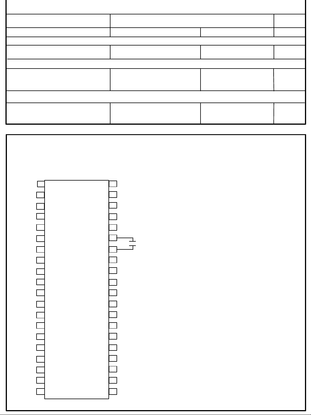
EXTERNAL CONNECTIONS
N.C.
N.C.
N.C.
Vee (-15V)
Vee (+15V)
Vdd (+5V)
GND
N.C.
N.C.
N.C.
1
2
3
4
5
6
7
8
9
10
(TOP VIEW)
ADC100
40
ANALOG LOW
39
ANALOG HIGH
38
N.C.
37
N.C.
36
N.C.
35
34
33
N.C.
N.C.
32
31
N.C.
MIN
-55
0
+14
-14
+4
V
EE
0
INTEGRATION
CAPACITOR
ADC100
MAX
125
160
+16
-16
+6
V
CC
V
DD
NOTES:
1. Power Supply Decoupling
The ADC100 has internal 0.1µF decoupling
capacitors for all power supply inputs. The
internal decoupling capacitors are adequate
for applications with relatively short power
supply leads (approx. 5") or if additional
capacitors are located on a circuit board.
For applications with long power supply
leads an external capacitor of 10 mF on the
+/- 15V inputs and 33 mF on the +5V input is
recommended.
2. Ground
The ground connection (pin 7) should be
made as solid as possible since ground
noise can result in a loss of accuracy. Use
of a ground plane is a good approach to
maintain the full accuracy of the ADC100.
UNITS
°C
°C
VDC
VDC
VDC
N.C.
N.C.
D0
D1
D2
D3
D4
D5
D6
D7
11
12
13
14
15
16
17
18
19
20
30
N.C.
AUTO ZERO
29
RESET
N.C.
28
N.C.
27
N.C.
26
25
N.C.
24
STATUS 1
23
STATUS 0
CONVERT
22
21
OUTPUT ENABLE
3. External Components
A 0.68 µF polystyrene integration capacitor
must be connected to pins 34 and 35 with a
lead length not exceeding 2".
4. Analog Inputs
In order to avoid differential noise pickup it is
recommended to use parallel adjacent lines
for the analog inputs (pins 39, 40) on PC
boards and shielded lines outside of the PC
connections.
ADC100DS REV. E MAR 00
Page 3
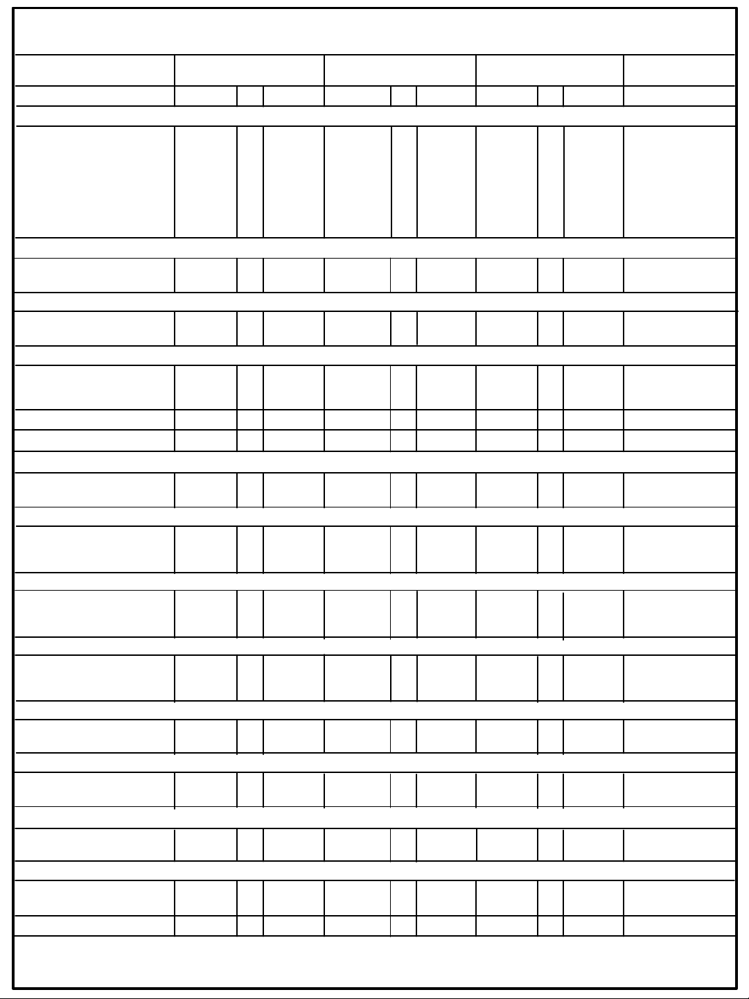
ELECTRICAL SPECIFICATIONS
(Vps = +/- 15V, + 5V, T = 25 Deg. C.)
ADC100
MODEL
PARAMETER
ACCURACY
Resolution
Input Equivalent Noise
Offset without Auto Zero
Offset with Auto Zero
Full Scale
Noise (.1-10Hz) @ 10V
Nonlinearity
Normal Mode Rejection
TEMPERATURE STABILITY
Offset
Full Scale
TIME STABILITY
Offset
Full Scale
ERROR ALL SOURCES
24 hrs, +/- 1 Deg. C Amb.
90 days, +/- 5 Deg. C Amb.
1 year, +/- 5 Deg. C Amb.
CONVERSION TIME
WARM-UP TIME
POWER SUPPLY REJECTION
+/- 15 VDC
5 VDC
ANALOG INPUT CHARACTERISTICS
Input Range -10.485760 10.485755
Bias Current 1.2
Input Impedance 200
POWER SUPPLY VOLTAGES
+15 V
-15 V
POWER SUPPLY CURRENTS
+15 V
-15 V
DIGITAL INPUTS
Low
High
DIGITAL OUTPUTS
Low
High
AUTO ZERO INPUT
Low
High
CONVERT INPUT
Low
High
TEMPERATURE RANGE
* Same as ADC100C
Note: 1) 60 Cycle
2
5 v
5 v
2) ( Max-Min Value) - Noise(.1-10Hz)
1
ADC100C
MIN MAXTYP MIN MAXTYP MIN MAXTYP
22
1
6
60
.1
2
80
80
14.5 15 15.5 * * * * * * V
14.5
4.5
4.0
4.0
4.0 * *
4.0 *
-25
15 15.5
5
23
24
42
ADC100CA ADC100M
*
4
1
100
3
*
0.2 0.1
1.0 0.5
.0007, 2 .0005, 2 %, +/- Counts
.0010, 2 .0008, 2
.0015, 2
320 ms
5
* * dB
* * dB
3
5.5
0.8
0.8
0.8
0.8
85 *
* * * *
* * * * * *
* * * * * *
* *
* *
*
*
2
0.5
50
*
2
*
*
*
.0013, 2
*
* *
* *
* *
* * mA
* *
* *
*
* *
* *
*
*
-55
*
*
*
*
*
*
*
*
*
*
*
*
*
*
*
*
*
125
ADC100DS REV. E MAR 00
Bits
µV
ppm
ppm
ppm
µVpp
ppm
dB
ppm/oC
ppm/oC
ppm/month
ppm/24 hrs.
%, +/- Counts
%, +/- Counts
minutes
V
nA
GΩ
V
V
mA
mA
V
V
V
V
V
V
V
V
o
C
Page 4

THEORY OF OPERATION
In the ADC100 block diagram (see Figure 1), V
and V
into a differential, voltage controlled, single output
current source. This current is added to the
reference current at the input of the op amp
integrator. The output of the integrator is fed into
a Schmitt trigger, which in turn, is fed into the
ADC's timing control circuitry. When the
integrator output actuates the Schmitt trigger, the
timing circuit changes the direction of the
reference current source and the integrator
begins integrating in the opposite direction. This
continues until the Schmitt trigger is actuated
again by the integrator and reverses the direction
of the reference current.
The equation for integration times are:
Resolving these equations produces:
are the inputs. Both are buffered and fed
low
V X C
Tp=
I ref + I inp
V = Voltage
C= Integration Capacitor Value
I ref = Reference Current
I inp = Input Current
I inp = I ref
Tp = Time Positive
Tm = Time Negative
Tp - Tm
Tp + Tm
Tm=
V X C
-I ref + I inp
hi
The timing control circuitry governs the counters that
measure the integration time in both directions.
The ADC100's on-board microprocessor is used to
calculate the results of the integration equation above.
It is also used to perform error corrections and to
control the built-in-auto-zero function. Note that the
mP automatically performs an auto-zero function at
start-up, but it is recommended, to achieve maximum
accuracy, that an auto-zero be performed again after
the ADC100 is fully warmed up.
When the µP detects a convert signal, it lowers the
status lines to indicate that the ADC is involved in a
conversion. When it detects a change in slope
direction, the µP will collect the counts for the
integration time. When sufficient counts have been
collected, the µP performs the calculations described
above.
When the calculations are complete, the µmP places
the most significant byte in the output buffer and
raises the S0flag. When another pulse is placed on
the convert line, the middle byte is placed on the
output, the S0flag is lowered and the S1flag raised.
When the last pulse is placed in the convert line, the
least significant byte is placed in the output buffer and
both status flags are high indicating that the ADC100
is ready for another conversion.
Status line summary:
S1S
0 0
0 1
1 0
1 1
0
Conversion in progress.
Conversion complete. MSB in output.
Middle byte in output register.
LSB in output. Ready for next conversion.
V
hi
Auto
Zero
Switch
V
low
Data
Output
FIGURE 1. BLOCK DIAGRAM
Output
Buffer
Output Enable
Differential
Voltage Controlled
Current Source
Microprocessor
ïï
Auto
Zero
Bidirectional
Reference
Current Source
Convert
Status
Lines
ï
Current
Directional
Switch
Timing
Control
and
Counter
Schmitt
Trigger
+15V
-15V
Clock
ADC100DS REV. E MAR 00
Page 5

CONNECTING THE ADC100
POWER SUPPLIES
The power supply lines are connected to pins 4-7.
Pin 4 is -15V, pin 5 is +15v, pin 6 is +5V and pin 7 is
GND.
OUTPUT DATA LINES
The output data is available in byte form on pins
13-20. Pin 20 is the Most Significant Bit and pin 13
the Least Significant Bit. The data lines go to a high
impedance state when the Output Enable line is at a
logic one level.
OUTPUT ENABLE (PIN 21)
Data is placed on the Output Data Lines by a logic
zero on this line.
CONVERT (Pin22)
This line is used to initiate a conversion cycle and
to retrieve the output data. The status lines indicate
which function will be executed. The first pulse
(transition from logic one to logic zero) starts the
conversion cycle. Two subsequent pulses are used
to place the lower two bytes on the Output Data
Lines.
AUTO-ZERO / RESET (Pin 29)
A logic zero on this input will autozero the ADC1503 by internally connecting the analog high to analog
low. Since the µP is reset the status lines S1 and
S0 are tristate before going to the low position. The
status lines will remain low until the autozero is
complete.
INTEGRATION CAPACITOR (Pin 34, 35)
A .68 µF polystyrene capacitor must be connected
to these pins. Lead length should be as short as
possible and not exceed 2".
ANALOG INPUTS (Pin 39, 40)
Both analog inputs are buffered by op-amps and
have a common mode rejection of approximately
80dB. min. To maintain the full accuracy at the
ADC it is recommended to keep the input to analog
common to less than 0.1VDC.
STATUS LINES (Pins 23, 24)
These lines indicate the present state of the ADC. When the Convert line receives the first pulse in a
conversion cycle the Status Lines go to logic zero, indicating that a conversion cycle is in progress. When
the conversion is complete the microprocessor places the MSB of the output data in the output buffer and
then raises S0to a logic one, indicating that the MSB at the output data is available in the output buffer.
When the Convert Line is pulsed again the middle byte of the output data is placed in that output buffer and
S1changes to logic one and S0to logic zero. The third pulse places the LSB of the output data in the buffer
and both status lines go to the logic one. The converter is now ready for the next conversion cycle.
The table below shows a summary of the status code.
S1S
0 0
0 1
1 0
1 1
0
Conversion in progress.
Conversion complete. MSB in output.
Middle byte in output register.
LSB in output. Ready for next conversion.
OUTPUT DATA REPRESENTATION
The output data is represented in BOB (Bipolar Offset Binary)
format. One LSB is scaled to be exactly 5mV. The table below
shows the output data codes for zero and plus-minus full scale
input voltage.
Input Voltage
-10.485760 V
0.0 V
+10.485755 V
High Byte Middle Byte Low Byte
00
20
3F
Output Data
00
00
FF
00
00
FF
ADC100DS REV. E MAR 00
Page 6

TIMING DIAGRAMS
CONVERT
AZ
S1
S0
t
TRST
Symbol Parameter Min. Typ. Max. Unit
t
AZD
t
TRST
t
AZ
FIGURE 2. AUTO ZERO
→
→
→
t
AZD
→
t
AZ
AZ Pulse Width 0.2 µs
Tristate Time 30 ms
AZ Time 400 ms
→
CONVERT
S1
t
→
SZ
S0
Symbol Parameter Min. Typ. Max. Unit
t
CONZ
t
SZ
t
CONV
FIGURE 3. CONVERSION
→
t
CONZ
→
t
CONV
Convert Pulse 5.0 µs
Status Delay 8.0 µs
Convert Time 320 ms
ADC100DS REV. E MAR 00
Page 7

OE
TIMING DIAGRAMS
D0 - D7
CONVERT
t
→
OEDV
S1
S0
Symbol Parameter Min. Typ. Max. Unit
t
OEDV
t
SIR
FIGURE 4. DATA OUTPUT
MSB
MIB
LSB
→
t
SIR
OE Delay 45 ns
Status Delay 3.0 µs
→
→
→
→
t
SIR
DIM
E
D
A
L
B2
B
Q
C
P
G1
B1
40-PIN HYBRID PACKAGE
INCHES
MIN
1.080
2.075
0.155
0.220
.100 typ
.018 typ
.015
.009
.012
.890
.040 typ
MAX
1.100
2.115
0.185
0.240
.035
.012
.018
.910
FIGURE 5. MECHANICAL SPECIFICATIONS
NOTES:
1. GOLD PLATING 60 MICRO INCHES MINIMUM
THICKNESS OVER 100 MICRO INCHES NOMINAL
THICKNESS OF NICKEL
ADC100DS REV. E MAR 00
 Loading...