

Page 1
ADC1005
10-Bit µP Compatible A/D Converter
ADC1005 10-Bit µP Compatible A/D Converter
June 1999
General Description
The ADC1005 is a CMOS 10-bit successive approximation
A/D converter.The 20-pin ADC1005 outputs 10-bit data in a
two-byte format for interface with 8-bit microprocessors.
The ADC1005 has differential inputs to permit rejection of
common-mode signals, allow the analog input range to be
offset, and also to permit the conversion of signals not referred to ground. In addition, the reference voltage can be
adjusted, allowing smaller voltage spans to be measured
with 10-bit resolution.
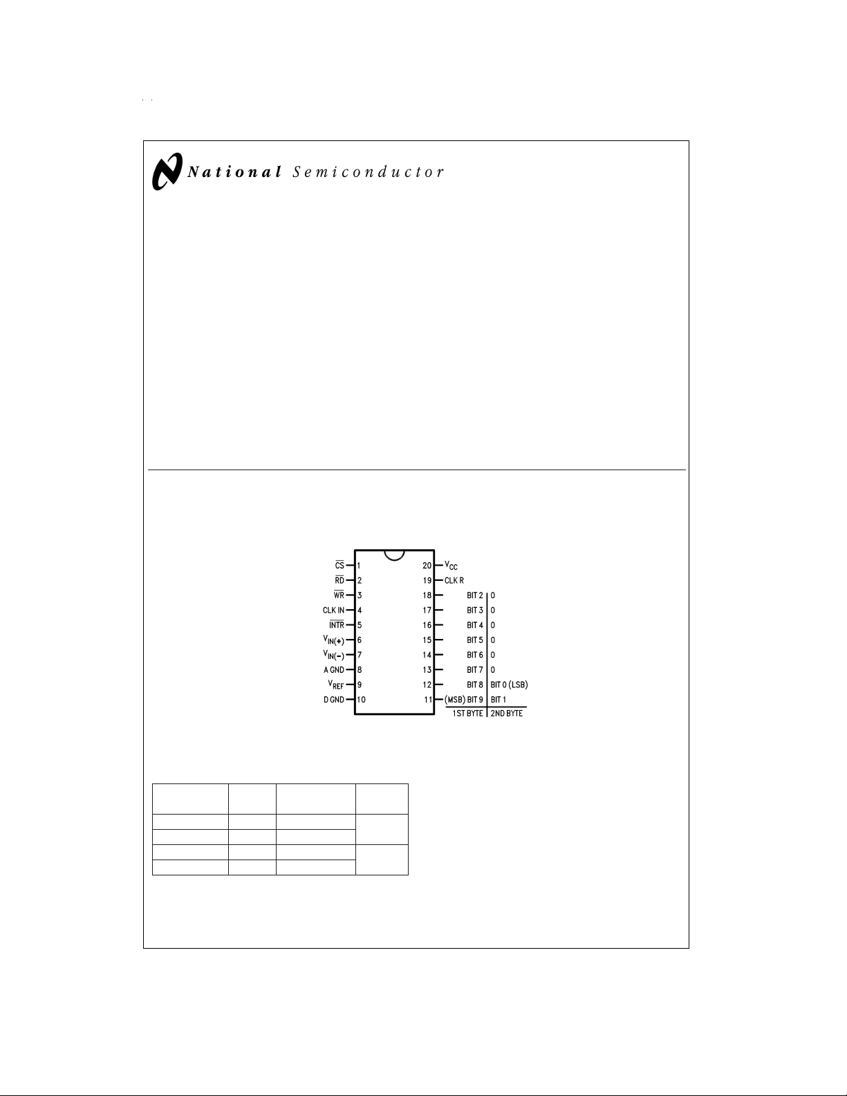
Connection Diagram
ADC 1005 (for an 8–bit data bus)
Dual-In-Line Package
Features
n Easy interface to all microprocessors
n Differential analog voltage inputs
n Operates ratiometrically or with 5 V
or analog span adjusted voltage reference
n 0V to 5V analog input voltage range with single 5V
supply
n On-chip clock generator
n TLL/MOS input/output compatible
n 0.3" standard width 20-pin DIP
voltage reference
DC
Key Specifications
n Resolution 10 bits
n Linearity Error
n Conversion Time 50 µs
1
±
⁄2LSB and±1 LSB
DS005261-1
Top View
Ordering Information
Part Number Package Temperature Linearity
Outline Range Error
ADC1005BCJ-1 J20A 0˚C to +70˚C
ADC1005BCJ J20A −40˚C to +85˚C
ADC1005CCJ-1 J20A 0˚C to +70˚C
ADC1005CCJ J20A −40˚C to +85˚C
TRI-STATE®is a registered trademark of National Semiconductor Corporation.
© 1999 National Semiconductor Corporation DS005261 www.national.com
1
±
±
⁄2LSB
1 LSB
Page 2
Absolute Maximum Ratings (Notes 1, 2)
If Military/Aerospace specified devices are required,
please contact the National Semiconductor Sales Office/
Distributors for availability and specifications.
Supply Voltage (V
Logic Control Inputs −0.3V to +15V
Voltage at Other Inputs and Outputs −0.3V to V
Input Current Per Pin
Input Current Per Package
Storage Temperature Range −65˚C to +150˚C
Package Dissipation at T
Lead Temperature
(Soldering, 10 seconds)
) 6.5V
CC
CC
±
=
25˚C 875 mW
A
+0.3V
±
5mA
20 mA
Dual-In-Line Package (Ceramic) 300˚C
Surface Mount Package
Vapor Phase (60 seconds) 215˚C
Infrared (15 seconds) 220˚C
ESD Susceptibility (Note 8) 800V
Operating Ratings (Notes 1, 2)
Supply Voltage (V
Temperature Range T
ADC1005BCJ, ADC1005CCJ −40˚C≤TA≤+85˚C
ADC1005BCJ-1, ADC1005CCJ-1
) 4.5V to 6.0V
CC
MN≤TA≤TMAX
Electrical Characteristics
The following specifications apply for V
from T
MIN
to T
MAX
; All other limits T
=
5V, V
CC
=
=
T
A
j
Parameter Conditions ADC1005BCJ ADC1005BCJ-1, Limit
Converter Characteristics
Linearity Error (Note 3)
ADC1005BCJ
ADC1005BCJ-1
ADC1005CCJ
ADC1005CCJ-1, CCV
Zero Error
ADC1005BCJ
ADC1005BCJ-1
ADC1005CCJ
ADC1005CCJ-1, CCV
Fullscale Error
ADC1005BCJ
ADC1005BCJ-1
ADC1005CCJ
ADC1005CCJ-1, CCV
Reference MIN 4.8 2.2 4.8 2.4 2.2 kΩ
Input MAX 4.8 8.3 4.8 7.6 8.3 kΩ
Resistance
Common-Mode MIN V
Input (Note 4) MAX V
(+) or VIN(−) GND−0.05 GND−0.05 GND−0.05 V
IN
DC Common-Mode Over
Common-Mode
Error Input Range
=
±
Power Supply Sensitivity V
CC
V
REF
5V
=
DC
4.75V
%
5
25˚C.
REF
=
5V, f
=
1.8 MHz unless otherwise specified. Boldface limits apply
CLK
ADC1005CCJ ADC1005CCJ-1
Typ Tested Design Typ Tested Design
(Note 5) Limit Limit (Note 5) Limit Limit
(Note 6) (Note 7) (Note 6) (Note 7)
±
0.5 LSB
±
0.5
±
1 LSB
±
1
±
0.5 LSB
±
0.5
±
1 LSB
±
1
±
0.5 LSB
±
0.5
±
1 LSB
±
1
+0.05 VCC+0.05 VCC+0.05 V
CC
1
±
⁄
8
1
±
⁄
8
1
±
⁄
4
1
±
⁄
4
1
±
⁄
8
1
±
⁄
8
1
±
⁄
4
1
±
⁄
4
±
0.5 LSB
±
1 LSB
±
0.5 LSB
±
1 LSB
±
0.5 LSB
±
1 LSB
1
±
⁄
4
1
±
⁄
4
Units
LSB
LSB
www.national.com 2
Page 3
Electrical Characteristics (Continued)
The following specifications apply for V
from T
MIN
to T
MAX
; All other limits T
=
5V, V
CC
=
=
T
A
j
Parameter Conditions ADC1005BCJ ADC1005BCJ-1, Limit
DC Characteristics
Logical “1” Input V
V
IN(1)
Voltage MIN (except CLK
V
, Logical “0” Input V
IN(0)
Voltage MAX (Except CLK
I
, Logical “1” Input V
IN
=
5.25V 2.0 2.0 2.0 V
CC
=
CC
=
5.0V 0.005 1 0.005 1 1 µA
IN
)
IN
4.75V 0.8 0.8 0.8 V
)
IN
Current MAX
I
, Logical “0” Input V
IN
=
0V −0.005 −1 −0.005 −1 −1 µA
IN
Current MAX
V
, Minimum CLK
T+(MIN)
IN
Positive going Threshold 3.1 2.7 3.1 2.7 2.7 V
Voltage
V
, Maximum CLK
T(MAX)
IN
Positive going Threshold 3.1 3.5 3.1 3.5 3.5 V
Voltage
V
, Minimum CLK
T−(MIN)
IN
Negative going Threshold 1.8 1.5 1.8 1.5 1.5 V
Voltage
V
, Maximum CLK
T−(MAX)
IN
Negative going Threshold 1.8 2.1 1.8 2.1 2.1 V
Voltage
V
, Minimum CLK
H(MIN)
Hysteresis (V
V
, Maximum CLK
H(MAX)
Hysteresis (V
V
, Logical “1” V
OUT(1)
Output Voltage MIN I
V
, Logical “0” V
OUT(0)
Output Voltage MAX I
I
, TRI-STATE Output V
OUT
Current MAX V
I
, Output Source V
SOURCE
T+-VT−
T+-VT−
IN
)
IN
)
=
4.75V
CC
=
−360 µA 2.4 2.8 2.4 V
OUT
=
I
−10 µA 4.5 4.6 4.5 V
OUT
=
4.75V 0.4 0.34 0.4 V
CC
=
1.6 mA
OUT
=
0V −0.01 −3 −0.01 −0.3 −3 µA
OUT
=
5V 0.01 3 0.01 0.3 3 µA
OUT
=
0V −14 −6.5 −14 −7.5 −6.5 mA
OUT
Current MIN
I
, Output Sink V
SINK
=
5V 16 8.0 16 9.0 8.0 mA
OUT
Current MIN
I
, Supply Current MAX f
CC
=
1.8 MHz 1.5 3 1.5 2.5 3 mA
CLK
CS=“1”
25˚C.
REF
=
5V, f
=
1.8 MHz unless otherwise specified. Boldface limits apply
CLK
ADC1005CCJ ADC1005CCJ-1
Typ Tested Design Typ Tested Design
(Note 5) Limit Limit (Note 5) Limit Limit
(Note 6) (Note 7) (Note 6) (Note 7)
1.3 0.6 1.3 0.6 0.6 V
1.3 2.0 1.3 2.0 2.0 V
Units
www.national.com3
Page 4

AC Electrical Characteristics
The following specifications apply for V
its apply from T
MIN
to T
MAX
; All other limits T
=
5V, V
CC
Parameter Conditions (Note 5) Limit Limit Units
, Clock Frequency MIN 0.2 0.2 MHz
f
CLK
MAX 2.6 2.6 MHz
Clock Duty Cycle MIN 40 40
MAX 60 60
t
, Conversion Time MIN 80 80 1/f
C
MAX 90 90 1/f
MIN f
MAX f
t
, Minimum WR Pulse
W(WR)L
Width
, Access Time (Delay from
t
ACC
falling edge of RD to Output
Data Valid)
t
, TRI-STATE Control
1H,t0H
(Delay from Rising Edge of RD
to Hi-Z State)
t
, Delay from Falling
WI,tRI
Edge of WR or RD to Reset of
=
1.8 MHz 45 45 µs
CLK
=
1.8 MHz 50 50 µs
CLK
CS=0
CS=0
=
C
100 pF, R
L
=
=
10k, C
R
L
L
=
L
=
2k, C
100 pF 145 230 230 ns
L
R
INTR
, INTR to 1st Read Set-up
t
IRS
Time
C
, Capacitance of Logic
IN
Inputs
, Capacitance of Logic
C
OUT
Outputs
Note 1: Absolute Maximum Ratings indicate limits beyond which damage to the device may occur. DC and AC electrical specifications do not apply when operating
the device beyond its specified operating conditions.
Note 2: All voltages are measured with respect to ground.
Note 3: Linearity error is defined as the deviation of the analog value, expressed in LSBs, from the straight line which passes through the end points of the transfer
characteristic.
Note 4: For V
voltages one diode drop below ground or one diode drop greater thanV
can cause this input diode to conduct, especially at elevated temperatures, and cause errors for analog inputs near full-scale. The spec allows 50 mV forward bias
of either diode. This means that as long as the analog V
absolute 0 V
Note 5: Typicals are at 25˚C and represent most likely parametric norm.
Note 6: Tested and guaranteed to National’s AOQL (Average Outgoing Quality Level).
Note 7: Guaranteed, but not 100%production tested. These limits are not used to calculate outgoing quality levels.
Note 8: Human body model, 100 pF discharged through a 1.5 kΩ resistor.
DC
the digital output code will be 00 0000 0000. Two on-chip diodes are tied to each analog input which will forward conduct for analog input
IN(−)≥VIN(+)
to5VDCinput voltage range will therefore require a minimum supply voltage of 4.950 VDCover temperature variations, initial tolerance and loading.
IN
=
REF
=
=
T
25˚C.
A
j
5V,V
REF
=
= 20 ns unless otherwise specified. Boldface lim-
5V, t
r=tf
Typ Tested Design Limit
(Note 6) (Note 7)
100 150 150 ns
170 300 300 ns
=
2k
L
10 pF 125 200 ns
300 450 450 ns
400 550 550 ns
5 7.5 pF
5 7.5 pF
supply.Becareful,duringtestingatlowVCClevels (4.5V), as high level analog inputs (5V)
CC
does not exceed the supply voltage by more than 50 mV, the output code will be correct. To achieve an
%
%
CLK
CLK
www.national.com 4
Page 5

Functional Diagram
Typical Performance Characteristics
DS005261-3
Logic Input Threshold
Voltage vs Supply Voltage
Output Current vs
Temperature
DS005261-21
Delay from Falling Edge of
RD to Output data Valid vs
Load Capacitance
DS005261-24
DS005261-22
Typical Linearity Error
vs Clock Frequency
CLK IN Schmitt Trip Levels
vs Supply Voltage
DS005261-23
DS005261-25
www.national.com5
Page 6

Timing Diagrams
Start Conversion
DS005261-5
Output Enable and Reset INTR
Note: All timing is measured from the 50%voltage points.
Byte Sequencing for ADC1005
Byte 8-Bit Data Bus Connection
Order DB7 DB6 DB5 DB4 DB3 DB2 DB1 DB0
MSB
1st Bit 9 Bit 8 Bit 7 Bit 6 Bit 5 Bit 4 Bit 3 Bit 2
2ndBit1Bit0000000
DS005261-6
LSB
www.national.com 6
Page 7

Block Diagram
Note 9: CS shown twice for clarity.
Note 10: SAR=Successive Approximation Register.
Functional Description
1.0 GENERAL OPERATION
Figure 1
IN
.All
(+) –
Ablock diagram of the A/D converter is shown in
of the inputs and outputs are shown and the major logic control paths are drawn in heavier weight lines.
1.1 Converter Operation
The ADC1005 uses an advanced potentiometric resistive
ladder network. The analog inputs, as well as the taps of this
ladder network are switched into a weighted capacitor array.
The output of this capacitor array is the input to a sampled
data comparator. This comparator allows the successive approximation logic to match the analog input voltage [V
V
(−)] to taps on the R network. The most significant bit is
IN
tested first and after 10 comparisons (80 clock cycles) a digital 10-bit binary code (all “1”s=full-scale) is transferred to an
output latch.
1.2 Starting a Conversion
The conversion is initialized by taking CS and WR simultaneously low. This sets the start flip-flop (F/F) and the resulting “1” level resets the 10-bit shift register, resets the interrupt (INTR) F/F and inputs a “1” to the D flop, F/F1, which is
FIGURE 1.
at the input end of the 10-bit shift register. Internal clock signals then transfer this “1” to the Q ouput of F/F1. The AND
gate, G1, combines this “1” output with a clock signal to provide a reset signal to the start F/F. If the set signal is no
longer present (either WR or CS is a “1”) the start F/F is reset
and the 10-bit shift register then can have the “1” clocked in,
allowing the conversion process to continue. If the set signal
were still present, this reset pulse would have no effect and
the 10-bit shift register would continue to be held in the reset
mode. This logic therefore allows for wide CS and WR signals. The converter will start after at least one of these signals returns high and the internal clocks again provide a reset signal for the start F/F.
To summarize, on the high-to-low transition of the WR input
the internal SAR latches and the shift register stages are reset. As long as the CS input and WR input remain low, the
A/D will remain in a reset state.
Conversion will start after at
least one of these inputs makes a low-to-high transition.
1.3 Output Control
After the “1” is clocked through the 10-bit shift register (which
completes the SAR search) it causes the new digital word to
transfer to the TRI-STATE output latches. When the XFER
DS005261-11
www.national.com7
Page 8

Functional Description (Continued)
signal makes a high-to-low transition the one shot fires, setting the INTR F/F.An inverting buffer then supplies the INTR
output signal.
Note that this SET control of the INTR F/F remains low for
approximately 400 ns. If the data output is continuously enabled (CS and RD both held low) the INTR output will still
signal the end of the conversion (by a high-to-low transition).
This is because the SET input can control the Q output of the
INTR F/F even though the RESET input is constantly at a “1”
level. This INTR output will therefore stay low for the duration
of the SET signal.
When data is to be read, the combination of both CS and RD
being low will cause the INTR F/F to be reset and the
TRI-STATE output latches will be enabled.
1.4 Free-Running and Self-Clocking Modes
For operation in the free-running mode an initializing pulse
should be used, following power-up, to ensure circuit operation. In this application, the CS input is grounded and the WR
input is tied to the INTR output. This WR and INTR node
should be momentarily forced to logic low following a
power-up cycle to ensure start up.
The clock for the A/D can be derived from the CPU clock or
an external RC can be added to provide self-clocking. The
CLK IN makes use of a Schmitt trigger as shown in
Figure 2
can be biased with a time and temperature stable voltage
source. The LM385 and LM336 reference diodes are good
low current devices to use with these converters.
The maximum value of the reference is limited to the V
supply voltage. The minimum value, however, can be small
to allow direct conversions of transducer outputs providing
less than a 5V output span. Particular care must be taken
with regard to noise pickup, circuit layout, and system error
voltage sources when operating with a reduced span due to
the increased sensitivity of the converter (1 LSB equals
V
/1024).
REF
.
DS005261-17
FIGURE 3. Ratiometric
CC
DS005261-12
FIGURE 2. Self-Clocking the A/D
2.0 REFERENCE VOLTAGE
The voltage applied to the reference input of these converters defines the voltage span of the analog input (the difference between V
possible output codes apply. The devices can be used in ei-
IN(MAX)
and V
) over which the 1024
IN(MIN)
ther ratiometric applications or in systems requiring absolute
accuracy.The reference pin must be connected to a voltage
source capable of driving the reference input resistance of
typically 4.8 kΩ. This pin is the top of a resistor divider string
used for the successive approximation conversion.
In a ratiometric system (
Figure 3
) the analog input voltage is
proportional to the voltage used for the A/D reference. This
voltage is typically the system power supply, so the V
can be tied to V
quirements of the system references as the analog input and
. This technique relaxes the stability re-
CC
REF
pin
A/D reference move together maintaining the same output
code for a given input condition.
For absolute accuracy (
Figure 4
), where the analog input
varies between very specific voltage limits, the reference pin
www.national.com 8
DS005261-18
FIGURE 4. Absolute with a Reduced Span
3.0 THE ANALOG INPUTS
3.1 Analog Differential Voltage Inputs and
Common-Mode Rejection
The differential inputs of these converters reduce the effects
of common-mode input noise, which is defined as noise
common to both selected “+” and “−” inputs (60 Hz is most
typical). The time interval between sampling the “+” input
and the “−” input is half of an internal clock period. The
Page 9

Functional Description (Continued)
change in the common-mode voltage during this short time
interval can cause conversion errors. For a sinusoidal
common-mode signal, this error is:
where fCMis the frequency of the common-mode signal,
V
is its peak voltage value and f
PEAK
quency at the CLK IN pin.
For a 60 Hz common-mode signal to generate a
(1.2 mV) with the converter running at 1.8 MHz, its peak
value would have to be 1.46V. A common-mode signal this
large is much greater than that generally found in data aquisition systems.
3.2 Input Current
Due to the sampling nature of the analog inputs, short duration spikes of current enter the “+” input and exit the “−” input
at the clock rising edges during the conversion. These currents decay rapidly and do not cause errors as the internal
comparator is strobed at the end of a clock period.
3.3 Input Bypass Capacitors
Bypass capacitors at the inputs will average the current
spikes noted in 3.2 and cause a DC current to flow through
the output resistances of the analog signal sources. This
charge pumping action is worse for continuous conversions
with the V
conversions with a 1.8 MHz clock frequency with the V
(+) input voltage at full scale. For continuous
IN
input at 5V, this DC current is at a maximum of approximately 5 µA. Therefore,
used at the analog inputs or the V
>
sources (
1kΩ). If input bypass capacitors are necessary
bypass capacitors should not be
REF
for noise filtering and high source resistance is desirable to
minimize capacitor size, the detrimental effects of the voltage drop across this input resistance, which is due to the average value of the input current, can be eliminated with a
full-scale adjustment while the given source resistor and input bypass capacitor are both in place. This is possible because the average value of the input current is a linear function of the differential input voltage.
3.4 Input Source Resistance
Large values of source resistance where an input bypass capacitor is not used,
will not cause errors
settle out prior to the comparison time. If a low pass filter is
required in the system, use a low valued series resistor (≤1
kΩ) for a passive RC section or add an op amp RC active
low pass filter. For low source resistance applications (≤0.1
kΩ) a 4700 pF bypass capacitor at the inputs will prevent
pickup due to series lead induction of a long wire. A 100Ω series resistor can be used to isolate this capacitor – both the
R and the C are placed outside the feedback loop – from the
output of an op amp, if used.
3.5 Noise
The leads to the analog inputs (pins 6 and 7) should be kept
as short as possible to minimize input noise coupling. Both
noise and undesired digital clock coupling to these inputs
can cause system errors. The source resistance for these inputs should, in general, be kept below 1 kΩ. Larger values of
source resistance can cause undesired system noise
is the clock fre-
CLK
1
⁄4LSB error
pin
for high resistance
if the input currents
(+)
IN
pickup. Input bypass capacitors, placed from the analog inputs to ground, can reduce system noise pickup but can create analog scale errors. See section 3.2, 3.3, and 3.4 if input
filtering is to be used.
4.0 OFFSET AND REFERENCE ADJUSTMENT
4.1 Zero Offset
The zero error of the A/D converter relates to the location of
the first riser of the transfer function and can be measured by
grounding the V(−) input and applying a small magnitude
positive voltage to the V(+) input. Zero error is the difference
between the actual DC input voltage that is necessary to just
cause an output digital code transition from 00 0000 0000 to
00 0000 0001 and the ideal
=
for V
REF
5.0 V
DC
1
⁄2LSB value (1⁄2LSB=2.45 mV
).
The zero of the A/D normally does not require adjustment.
However, for cases where V
duced span applications (V
may be desired. The converter can be made to output an all
is not ground and in re-
IN(MIN)
<
5V), an offset adjustment
REF
zero digital code for an arbitrary input by biasing the A/D’s
V
(−) input at that voltage. This utilizes the differential input
IN
operation of the A/D.
4.2 Full Scale
The full-scale adjustment can be made by applying a differential input voltage that is 1
1
⁄2LSB down from the desired
analog full-scale voltage range and then adjusting the magnitude of the V
changing from 11 1111 1110 to 11 1111 1111.
input for a digital output code that is just
REF
4.3 Adjusting for an Arbitrary Analog
Input Voltage Range
If the analog zero voltage of the A/D is shifted away from
ground (for example, to accommodate an analog input signal
that does not go to ground), this new zero reference should
be properly adjusted first. A V
desired zero reference plus
(+) voltage that equals this
IN
1
⁄2LSB (where the LSB is calcu-
lated for the desired analog span, 1 LSB=analog span/
1024) is applied to selected “+” input and the zero reference
voltage at the corresponding “−” input should then be adjusted to just obtain the 000
HEX
001
HEX
code transition.
The full-scale adjustment should be made [with the proper
V
(−) voltage applied] by forcing a voltage to the VIN(+) in-
IN
put given by:
where V
V
MIN
(Both are ground referenced).
The V
change from 3FF
ment procedure.
=
the high end of the analog input range and
MAX
=
the low end (the offset zero) of the analog range.
(or VCC) voltage is then adjusted to provide a code
REF
HEX
to 3FE
. This completes the adjust-
HEX
For an example see the Zero-Shift and Span-Adjust circuit
below.
5.0 POWER SUPPLIES
Noise spikes on the V
errors as the comparator will respond to this noise. A low in-
supply line can cause conversion
CC
ductance tantalum filter capacitor should be used close to
the converter V
ommended. If an unregulated voltage is available in the sys-
pin and values of 1 µF or greater are rec-
CC
www.national.com9
Page 10

Functional Description (Continued)
tem, a separate LM340LAZ-5.0, TO-92, 5V voltage regulator
for the converter (and the other analog circuitry) will greatly
reduce digital noise on the V
A single point analog ground that is separate from the logic
ground points should be used. The power supply bypass ca-
supply.
CC
FIGURE 5. Zero-Shift and Span-Adjust (2V ≤ VIN≤ 5V)
pacitor and the self-clocking capacitor (if used) should both
be returned to the digital ground. Any V
tors, analog input filters capacitors, or input signal shielding
bypass capaci-
REF
should be returned to the analog ground point.
DS005261-16
Typical Applications
www.national.com 10
DS005261-13
Page 11

Typical Applications (Continued)
Operating with Ratiometric Transducers
VIN(−)=0.15 V
15%of VCC≤ V
CC
XDR
≤ 85%of V
CC
TRI-STATE Test Circuits and Waveforms
t
1H
DS005261-7
=
t
20 ns
r
DS005261-14
Handling±5V Analog Inputs
=
tIH,C
10 pF
L
DS005261-9
DS005261-15
t
0H
DS005261-8
=
t
20 ns
r
tIH,C
L
=
10 pF
DS005261-10
www.national.com11
Page 12

Physical Dimensions inches (millimeters) unless otherwise noted
ADC1005 10-Bit µP Compatible A/D Converter
Hermetic Dual-In-Line Package (J)
Order Number ADC1005BCJ, ADC1005BCJ-1,
ADC1005CCJ or ADC1005CCJ-1
NS Package Number J20A
LIFE SUPPORT POLICY
NATIONAL’S PRODUCTS ARE NOT AUTHORIZED FOR USE AS CRITICAL COMPONENTS IN LIFE SUPPORT
DEVICES OR SYSTEMS WITHOUT THE EXPRESS WRITTEN APPROVAL OF THE PRESIDENT AND GENERAL
COUNSEL OF NATIONAL SEMICONDUCTOR CORPORATION. As used herein:
1. Life support devices or systems are devices or
systems which, (a) are intended for surgical implant
into the body, or (b) support or sustain life, and
whose failure to perform when properly used in
accordance with instructions for use provided in the
2. A critical component is any component of a life
support device or system whose failure to perform
can be reasonably expected to cause the failure of
the life support device or system, or to affect its
safety or effectiveness.
labeling, can be reasonably expected to result in a
significant injury to the user.
National Semiconductor
Corporation
Americas
Tel: 1-800-272-9959
Fax: 1-800-737-7018
Email: support@nsc.com
www.national.com
National Semiconductor
Europe
Fax: +49 (0) 1 80-530 85 86
Email: europe.support@nsc.com
Deutsch Tel: +49 (0) 1 80-530 85 85
English Tel: +49 (0) 1 80-532 78 32
Français Tel: +49 (0) 1 80-532 93 58
Italiano Tel: +49 (0) 1 80-534 16 80
National Semiconductor
Asia Pacific Customer
Response Group
Tel: 65-2544466
Fax: 65-2504466
Email: sea.support@nsc.com
National Semiconductor
Japan Ltd.
Tel: 81-3-5639-7560
Fax: 81-3-5639-7507
National does not assume any responsibility for use of any circuitry described, no circuit patent licenses are implied and National reserves the right at any time without notice to change said circuitry and specifications.
 Loading...