

Page 1
ADC1001
10-Bit µP Compatible A/D Converter
ADC1001 10-Bit µP Compatible A/D Converter
June 1999
General Description
The ADC1001 is a CMOS, 10-bit successive approximation
A/D converter. The 20-pin ADC1001 is pin compatible with
theADC08018-bitA/D family.The 10-bit data word is read in
two 8-bit bytes, formatted left justified and high byte first. The
six least significant bits of the second byte are set to zero, as
is proper for a 16-bit word.
Differential inputs provide low frequency input common
mode rejection and allow offsetting the analog range of the
converter. In addition, the reference input can be adjusted
enabling the conversion of reduced analog ranges with
10-bit resolution.
Key Specifications
n Resolution 10 bits
n Linearity error
n Conversion time 200µS
±
1 LSB
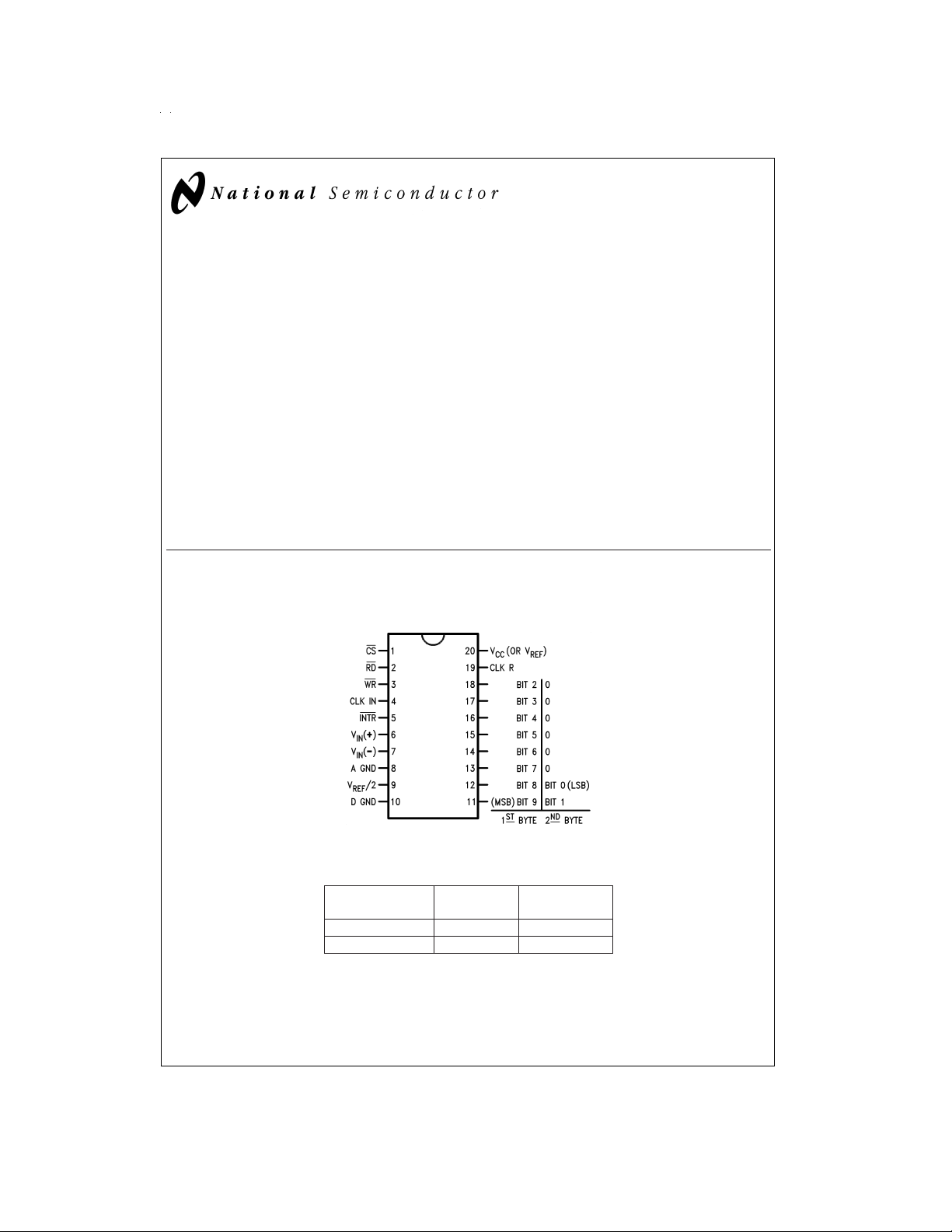
Connection Diagram
ADC1001
Dual-In-Line Package
Features
n ADC1001 is pin compatible with ADC0801 series 8-bit
A/D converters
n Compatible with NSC800 and 8080 µP derivatives — no
interfacing logic needed
n Easily interfaced to 6800 µP derivatives
n Differential analog voltage inputs
n Logic inputs and outputs meet both MOS and TTL
voltage level specifications
n Works with 2.5V (LM336) voltage reference
n On-chip clock generator
n 0V to 5V analog input voltage range with single 5V
supply
n Operates ratiometrically or with 5 V
analog span adjusted voltage reference
n 0.3" standard width 20-pin DIP package
, 2.5 VDC,or
DC
DS005675-11
Top View
Ordering Information
Temperature
Range
Order Number ADC1001CCJ-1 ADC1001CCJ
Package Outline J20A J20A
TRI-STATE®is a registered trademark of National Semiconductor Corp.
© 1999 National Semiconductor Corporation DS005675 www.national.com
0˚C to +70˚C −40˚C to +85˚C
Page 2
Absolute Maximum Ratings (Notes 1, 2)
If Military/Aerospace specified devices are required,
please contact the National Semiconductor Sales Office/
Distributors for availability and specifications.
Supply Voltage (V
Logic Control Inputs −0.3V to +18V
Voltage at Other Inputs and Outputs −0.3V to (V
Storage Temperature Range −65˚C to +150˚C
Package Dissipation at T
) (Note 3) 6.5V
CC
CC
=
25˚C 875 mW
A
+0.3V)
Lead Temp. (Soldering, 10 seconds) 300˚C
ESD Susceptibility (Note 10) 800V
Operating Conditions (Notes 1, 2)
Temperature Range T
ADC1001CCJ −40˚C≤TA≤+85˚C
ADC1001CCJ-1 0˚C≤T
Range of V
CC
MIN≤TA≤TMAX
≤+70˚C
A
4.5 VDCto 6.3 V
DC
Converter Characteristics
Converter Specifications: V
=
5V
CC
DC,VREF
/2=2.500 VDC,T
MIN≤TA≤TMAX
Parameter Conditions MIn Typ Max Units
Linearity Error
Zero Error
Full-Scale Error
Total Ladder Resistance (Note 9) Input Resistance at Pin 9 2.2 4.8 KΩ
Analog Input Voltage Range (Note 4) V(+) or V(−) GND−0.05 V
DC Common-Mode Error Over Analog Input Voltage Range
=
Power Supply Sensitivity V
CC
Allowed V
5V
DC
IN
±
5%Over
(+) and VIN(−)
Voltage Range (Note 4)
and f
=
410 kHz unless otherwise specified.
CLK
CC
1
±
⁄
8
1
±
⁄
8
±
1 LSB
±
2 LSB
±
2 LSB
+0.05 V
LSB
LSB
AC Electrical Characteristics
Timing Specifications: V
=
5V
CC
DC
Symbol Parameter Conditions MIn Typ Max Units
T
c
f
CLK
Conversion Time (Note 5) 80 90 1/f
Clock Frequency (Note 8) 100 1260 kHz
Clock Duty Cycle 40 60
CR Conversion Rate In Free-Running INTR tied to WR with
Mode CS=0V
t
W(WR)L
Width of WR Input (Start Pulse CS=0VDC(Note 6) 150 ns
Width)
t
ACC
Access Time (Delay from C
Falling Edge of RD to Output
Data Valid)
t
1H,t0H
TRI-STATE®Control (Delay C
from Rising Edge of RD to
Hi-Z State) Circuits)
t
WI,tRI
Delay from Falling Edge 300 450 ns
of WR or RD to Reset of INTR
t
1rs
C
IN
INTR to 1st Read Set-Up Time 550 400 ns
Input Capacitance of Logic 5 7.5 pF
Control Inputs
C
OUT
TRI-STATE Output 5 7.5 pF
Capacitance (Data Buffers)
=
and T
25˚C unless otherwise specified.
A
f
CLK
L
L
(See TRI-STATE Test
=
410 kHz 195 220 µs
4600 conv/s
=
410 kHz
DC,fCLK
=
100 pF 170 300 ns
=
10 pF, R
=
10k 125 200 ns
L
CLK
%
DC
www.national.com 2
Page 3
DC Electrical Characteristics
The following specifications apply for V
Symbol Parameter Conditions MIn Typ Max Units
CONTROL INPUTS [Note: CLK IN is the input of a Schmitt trigger circuit and is therefore specified separately]
V
(1) Logical “1” Input Voltage V
IN
(Except CLK IN)
V
(0) Logical “0” Input Voltage V
IN
(Except CLK IN)
I
(1) Logical “1” Input Current V
IN
(All Inputs)
I
(0) Logical “0” input Current V
IN
(All Inputs)
CLOCK IN
V
+ CLK IN Positive Going 2.7 3.1 3.5 V
T
Threshold Voltage
V
− CLK IN Negative Going 1.5 1.8 2.1 V
T
Threshold Voltage
V
H
CLK IN Hysteresis 0.6 1.3 2.0 V
(VT+)−(VT−)
OUTPUTS AND INTR
V
(0) Logical “0” Output Voltage I
OUT
V
(1) Logical “1” Output Voltage I
OUT
I
OUT
TRI-STATE Disabled Output V
Leakage (All Data Buffers) V
I
SOURCE
I
SINK
POWER SUPPLY
I
CC
Supply Current (Includes f
Ladder Current) V
Note 1: AbsoluteMaximum Ratings indicate limits beyond which damage to the device may occur. DC and AC electrical specifications do not apply when operating
the device beyond its specified operating conditions.
Note 2: All voltages are measured with respect to GND, unless otherwise specified. The separate A GND point should always be wired to the D GND.
Note 3: Azener diode exists, internally, from V
Note 4: ForV
for analog input voltages one diode drop below ground or one diode drop greater than the V
level analog inputs (5V) can cause this input diode to conduct — especially at elevated temperatures, and cause errors for analog inputs near fullscale. The spec allows 50 mV forward bias of either diode. This means that as long as the analog V
be correct. Toachievean absolute 0 V
tolerance and loading.
Note 5: With an asynchronous start pulse, up to 8 clock periods may be required before the internal clock phases are proper to start the conversion process. The
start request is internally latched, see
Note 6: The CS input is assumed to bracket the WR strobe input and therefore timing is dependent on the WR pulse width. An arbitrarily wide pulse width will hold
the converter in a reset mode and the start of conversion is initiated by the low to high transition of the WR pulse (see Timing Diagrams).
Note 7: All typical values are for T
Note 8: Accuracy is guaranteed at f
Note 9: The V
of these two equal resistors.
Note 10: Human body model, 100 pF discharged through a 1.5 kΩ resistor.
(−)≥ VIN(+) the digital output code will be all zeros. Two on-chip diodes are tied to each analog input (see Block Diagram) which will forward conduct
IN
DC
Figure 3
=
25˚C.
A
=
pin is the center point of a two resistor divider (each resistor is 2.4kΩ) connected from VCCto ground. Total ladder input resistance is the sum
REF/2
CLK
=
and T
5V
CC
DC
CC
CC
=
IN
=
IN
OUT
=
−360 µA, V
O
=
I
−10 µA, V
O
OUT
OUT
V
OUT
V
OUT
CLK
REF
and CS=1
to GND and has a typical breakdown voltage of 7 VDC.
CC
to5VDCinput voltage range will therefore require a minimum supply voltage of 4.950 VDCover temperature variations, initial
.
410 kHz. At higher clock frequencies accuracy can degrade.
≤ T
MIN≤TA
=
5.25 V
DC
=
4.75 V
DC
5V
DC
0V
DC
=
1.6 mA, V
=
=
0.4 V
5V
CC
CC
=
CC
DC
DC
Short to GND, T
Short to VCC,T
=
410 kHz,
/2=NC, T
=
A
IN
, unless otherwise specified.
MAX
2.0 15 V
0.8 V
0.005 1 µA
−1 −0.005 µA
=
4.75 V
=
4.75 V
4.75 V
DC
DC
DC
2.4 V
4.5 V
0.4 V
0.1 −100 µA
0.1 3 µA
=
25˚C 4.5 6 mA
A
=
25˚C 9.0 16 mA
A
25˚C
2.5 5.0 mA
supply. Be careful, during testing at low VCClevels (4.5V), as high
CC
does not exceed the supply voltage by more than 50 mV,the output code will
DC
DC
DC
DC
DC
DC
DC
DC
DC
DC
DC
DC
DC
DC
www.national.com3
Page 4

Typical Performance Characteristics
Logic Input Threshold
Voltage vs Supply Voltage
Output Current vs
Temperature
DS005675-14
Delay From Falling Edge of
RD to Output Data Valid
vs Load Capacitance
DS005675-15
CLK IN Schmitt Trip Levels
vs Supply Voltage
DS005675-16
DS005675-17
TRI-STATE Test Circuits and Waveforms
DS005675-3
DS005675-5
www.national.com 4
=
t1H,C
10 pF
L
=
t
20 ns
r
=
t0H,C
L
=
t
20 ns
r
DS005675-4
10 pF
DS005675-6
Page 5

TRI-STATE Test Circuits and Waveforms (Continued)
Timing Diagrams
Output Enable and Reset INTR
DS005675-7
*All timing is measured from the 50%voltage points.
DS005675-8
www.national.com5
Page 6

Timing Diagrams (Continued)
Byte Sequencing For The 20-Pin ADC1001
Byte 8-Bit Data Bus Connection
Order DB7 DB6 DB5 DB4 DB3 DB2 DB1 DB0
MSB
1st Bit 9 Bit 8 Bit 7 Bit 6 Bit 5 Bit 4 Bit 3 Bit 2
LSB
2ndBit1Bit0000000
Functional Description
The ADC1001 uses an advanced potentiometric resistive
ladder network. The analog inputs, as well as the taps of this
ladder network, are switched into a weighted capacitor array.
The output of this capacitor array is the input to a sampled
data comparator.This comparator allows the successive approximation logic to match the analog difference input voltage [V
(+)−VIN(−)] to taps on the R network. The most sig-
IN
nificant bit is tested first and after 10 comparisons (80 clock
cycles) a digital 10-bit binary code (all “1”s=full-scale) is
transferred to an output latch and then an interrupt is asserted (INTR makes a high-to-low transition). The device
may be operated in the free-running mode by connecting
INTR to the WR input with CS=0. To ensure start-up under
all possible conditions, an external WR pulse is required during the first power-up cycle. A conversion in process can be
interrupted by issuing a second start command.
On the high-to-low transition of the WR input the internal
SAR latches and the shift register stages are reset. As long
as the CS input and WR input remain low,the A/D will remain
in a reset state.
Conversion will start from 1 to 8 clock periods after at least one of these inputs makes a low-to-high
transition.
A functional diagram of the A/D converter is shown in
3
.All of the inputs and outputs are shown and the major logic
Figure
control paths are drawn in heavier weight lines.
The conversion is initialized by taking CS and WR simulta-
neously low. This sets the start flip-flop (F/F) and the resulting “1” level resets the 8-bit shift register, resets the Interrupt
(INTR) F/F and inputs a “1” to the D flop, F/F1, which is at the
input end of the 10-bit shift register. Internal clock signals
then transfer this “1” to the Q output of F/F1. The AND gate,
G1, combines this “1” output with a clock signal to provide a
reset signal to the start F/F. If the set signal is no longer
present (either WR or CS is a “1”) the start F/F is reset and
the 10-bit shift register then can have the “1” clocked in,
which allows the conversion process to continue. If the set
signal were to still be present, this reset pulse would have no
effect and the 10-bit shift register would continue to be held
in the reset mode. This logic therefore allows for wide CS
and WR signals and the converter will start after at least one
of these signals returns high and the internal clocks again
provide a reset signal for the start F/F.
After the “1” is clocked through the 10-bit shift register (which
completes the SAR search) it causes the new digital word to
transfer to the TRI-STATE output latches. When this XFER
signal makes a high-to-low transition the one shot fires, setting the INTR F/F. An inverting buffer then supplies the INTR
output signal.
Note that this SET control of the INTR F/F remains low for
aproximately 400 ns. If the data output is continuously enabled (CS and RD both held low), the INTR output will still
signal the end of the conversion (by a high-to-low transition),
because the SET input can control the Q output of the INTR
F/F even though the RESET input is constantly at a “1” level.
This INTR output will therefore stay low for the duration of
the SET signal.
When data is to be read, the combination of both CS and RD
being low will cause the INTR F/F to be reset and the
TRI-STATE output latches will be enabled.
Zero and Full-Scale Adjustment
Zero error can be adjusted as shown in
forced to +2.5 mV (+
1
⁄2LSB) and the potentiometer is adjusted until the digital output code changes from 00 0000
0000 to 00 0000 0001.
Full-scale is adjusted as shown in
input. With V
1
less 1
(+) forced to the desired full-scale voltage
IN
⁄2LSBs (VFS−11⁄2LSBs), V
digital output code changes from 11 1111 1110 to 11 1111
1111.
Figure 1
.VIN(+) is
Figure 2
, with the V
/2 is adjusted until the
REF
REF
/2
www.national.com 6
Page 7

Functional Description (Continued)
Note 11: VIN(−) should be biased so that VIN(−)≥ −0.05V when potentiom-
eter wiper is set at most negative voltage position.
DS005675-9
FIGURE 1. Zero Adjust Circuit
Typical Application
DS005675-10
FIGURE 2. Full-Scale Adjust
DS005675-1
www.national.com7
Page 8

Block Diagram
Note 12: CS shown twice for clarity.
Note 13: SAR=Successive Approximation Register.
FIGURE 3.
www.national.com 8
DS005675-13
Page 9

Physical Dimensions inches (millimeters) unless otherwise noted
Cavity Dual-In-Line Package (J) (Side Brazed)
Order Number ADC1001CCJ or ADC1001CCJ-1
NS Package Number J20A
ADC1001 10-Bit µP Compatible A/D Converter
LIFE SUPPORT POLICY
NATIONAL’S PRODUCTS ARE NOT AUTHORIZED FOR USE AS CRITICAL COMPONENTS IN LIFE SUPPORT
DEVICES OR SYSTEMS WITHOUT THE EXPRESS WRITTEN APPROVAL OF THE PRESIDENT AND GENERAL
COUNSEL OF NATIONAL SEMICONDUCTOR CORPORATION. As used herein:
1. Life support devices or systems are devices or
systems which, (a) are intended for surgical implant
into the body, or (b) support or sustain life, and
whose failure to perform when properly used in
accordance with instructions for use provided in the
2. A critical component is any component of a life
support device or system whose failure to perform
can be reasonably expected to cause the failure of
the life support device or system, or to affect its
safety or effectiveness.
labeling, can be reasonably expected to result in a
significant injury to the user.
National Semiconductor
Corporation
Americas
Tel: 1-800-272-9959
Fax: 1-800-737-7018
Email: support@nsc.com
www.national.com
National does not assume any responsibility for use of any circuitry described, no circuit patent licenses are implied and National reserves the right at any time without notice to change said circuitry and specifications.
National Semiconductor
Europe
Fax: +49 (0) 1 80-530 85 86
Email: europe.support@nsc.com
Deutsch Tel: +49 (0) 1 80-530 85 85
English Tel: +49 (0) 1 80-532 78 32
Français Tel: +49 (0) 1 80-532 93 58
Italiano Tel: +49 (0) 1 80-534 16 80
National Semiconductor
Asia Pacific Customer
Response Group
Tel: 65-2544466
Fax: 65-2504466
Email: sea.support@nsc.com
National Semiconductor
Japan Ltd.
Tel: 81-3-5639-7560
Fax: 81-3-5639-7507
 Loading...