

Page 1
ADC0841
8-Bit µP Compatible A/D Converter
General Description
The ADC0841 is a CMOS 8-bit successive approximation
A/D converter.Differentialinputsprovidelowfrequencyinput
common mode rejection and allow offsetting the analog
range of the converter. In addition, the reference input can
be adjusted enabling the conversion of reduced analog
ranges with 8-bit resolution.
The A/D is designed to operate with the control bus of a variety of microprocessors. TRI-STATE
®
output latches that directly drive the data bus permit the A/D to be configured as
a memory location or I/O device to the microprocessor with
no interface logic necessary.
Features
n Easy interface to all microprocessors
n Operates ratiometrically or with 5 V
DC
voltage reference
n No zero or full-scale adjust required
n Internal clock
n 0V to 5V input range with single 5V power supply
n 0.3" standard width 20-pin package
n 20 Pin Molded Chip Carrier Package
Key Specifications
n Resolution: 8 Bits
n Total Unadjusted Error:
±
1
⁄2LSB and±1 LSB
n Single Supply: 5 V
DC
n Low Power: 15 mW
n Conversion Time: 40 µs
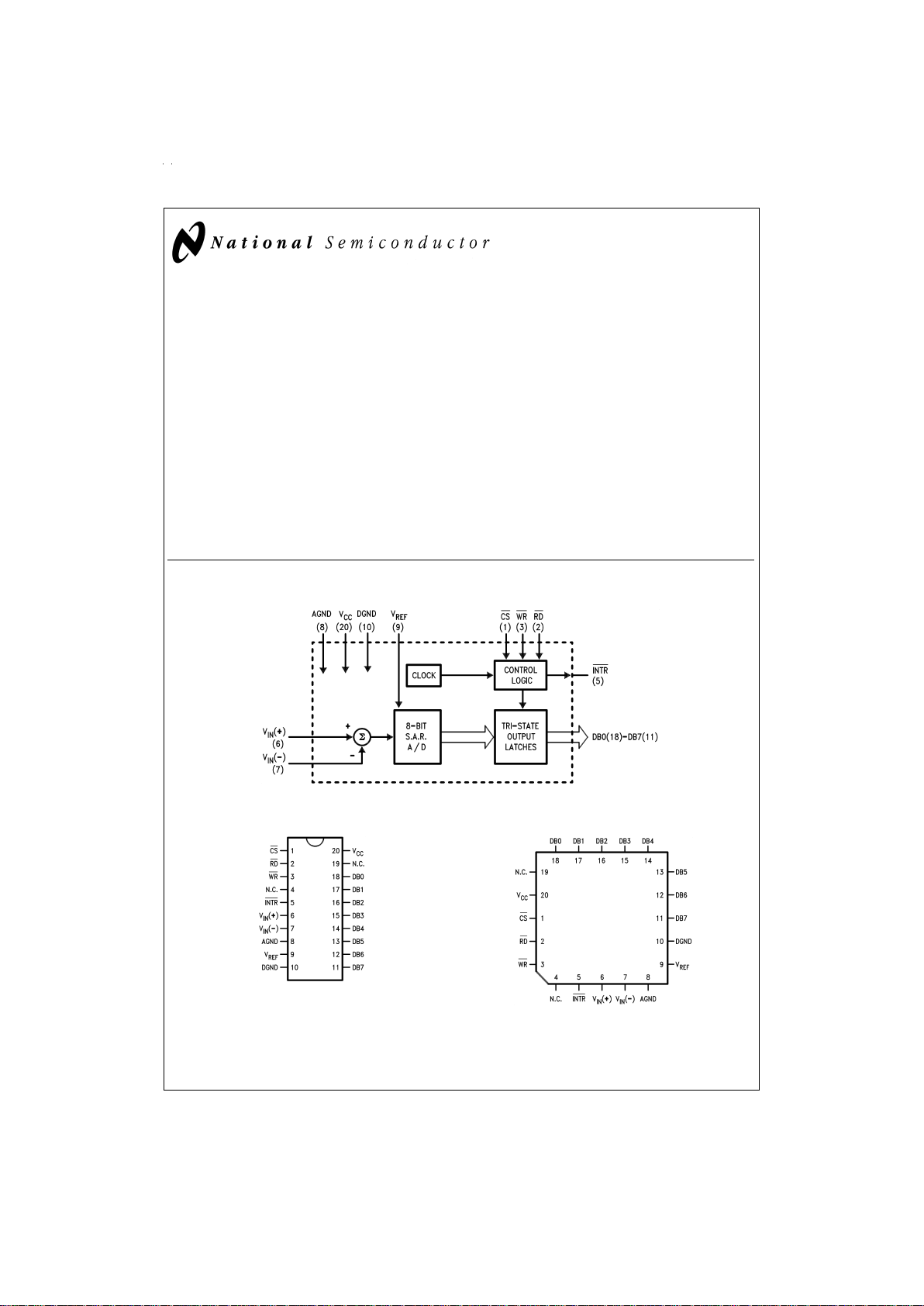
Block and Connection Diagrams
TRI-STATE®is a registered trademark of National Semiconductor Corporation.
NSC800
™
is a trademark of National Semiconductor Corporation.
DS008557-1
Dual-In-Line Package (N)
DS008557-2
(N.C.-No Connection)
Top View
Molded Chip Carrier Package (V)
DS008557-3
Top View
May 1998
ADC0841 8-Bit µP Compatible A/D Converter
© 1999 National Semiconductor Corporation DS008557 www.national.com
Page 2
Absolute Maximum Ratings (Notes 1, 2)
If Military/Aerospace specified devices are required,
please contact the National Semiconductor Sales Office/
Distributors for availability and specifications.
Supply Voltage (V
CC
) 6.5V
Voltage
Logic Control Inputs −0.3V to V
CC
+0.3V
At Other Inputs and Outputs −0.3V to V
CC
+0.3V
Input Current Per Pin (Note 3)
±
5mA
Input Current Per Package (Note 3)
±
20 mA
Storage Temperature −65˚C to +150˚C
Package Dissipation at T
A
=
25˚C 875 mW
Lead Temp. (Soldering, 10 seconds)
Dual-In-Line Package (Plastic)
Molded Chip Carrier Package
Vapor Phase (60 seconds)
Infrared (15 seconds)
260˚C
215˚C
220˚C
ESD Susceptibility (Note 10) 800V
Operating Conditions (Notes 1, 2)
Supply Voltage (V
CC
) 4.5 VDCto 6.0 V
DC
Temperature Range T
MIN≤TA≤TMAX
ADC0841BCN, ADC0841CCN 0˚C≤TA≤70˚C
ADC0841BCV, ADC0841CCV −40˚C≤T
A
≤85˚C
Electrical Characteristics
The following specifications apply for V
CC
=
5V
DC
unless otherwise specified. Boldface limits apply from T
MIN
to T
MAX
; all
other limits T
A
=
T
j
=
25˚C.
ADC0841BCN, ADC0841CCN
ADC0841BCV, ADC0841CCV
Parameter Conditions Typ Tested Design Units
(Note 6) Limit Limit
(Note 7) (Note 8)
CONVERTER AND MULTIPLEXER CHARACTERISTICS
Maximum Total V
REF
=
5.00 V
DC
Unadjusted Error (Note 4)
ADC0841BCN, BCV
±
1
⁄
2
±
1
⁄
2
LSB
ADC0841CCN, CCV
±
1
±
1 LSB
Minimum Reference 2.4 1.2 1.1 kΩ
Input Resistance
Maximum Reference 2.4 5.4 5.9 kΩ
Input Resistance
Maximum Common-Mode (Note 5) V
CC
+0.05 VCC+0.05 V
Input Voltage
Minimum Common-Mode (Note 5) GND−0.05 GND−0.05 V
Input Voltage
DC Common-Mode Error Differential Mode
±
1/16
±
1
⁄
4
±
1
⁄
4
LSB
Power Supply Sensitivity V
CC
=
5V
±
5
%
±
1/16
±
1
⁄
8
±
1
⁄
8
LSB
Electrical Characteristics
The following specifications apply for V
CC
=
5V
DC
unless otherwise specified. Boldface limits apply from T
MIN
to T
MAX
; all
other limits T
A
=
T
j
=
25˚C.
ADC0841BCN, ADC0841CCN
ADC0841BCV, ADC0841CCV
Symbol Parameter Conditions Typ Tested Design Units
(Note 6) Limit Limit
(Note 7) (Note 8)
DIGITAL AND DC CHARACTERISTICS
V
IN(1)
Logical “1” Input V
CC
=
5.25V 2.0 2.0 V
Voltage (Min)
V
IN(0)
Logical “0” Input V
CC
=
4.75V 0.8 0.8 V
Voltage (Max)
I
IN(1)
Logical “1” Input V
IN
=
5.0V 0.005 1 µA
Current (Max)
www.national.com 2
Page 3
Electrical Characteristics (Continued)
The following specifications apply for V
CC
=
5V
DC
unless otherwise specified. Boldface limits apply from T
MIN
to T
MAX
; all
other limits T
A
=
T
j
=
25˚C.
ADC0841BCN, ADC0841CCN
ADC0841BCV, ADC0841CCV
Symbol Parameter Conditions Typ Tested Design Units
(Note 6) Limit Limit
(Note 7) (Note 8)
DIGITAL AND DC CHARACTERISTICS
I
IN(0)
Logical “0” Input V
IN
=
0V −0.005 −1 µA
Current (Max)
V
OUT(1)
Logical “1” V
CC
=
4.75V
Output Voltage (Min) I
OUT
=
−360 µA 2.8 2.4 V
I
OUT
=
−10 µA 4.6 4.5 V
V
OUT(0)
Logical “0” V
CC
=
4.75V 0.34 0.4 V
Output Voltage (Max) I
OUT
=
1.6 mA
I
OUT
TRI-STATE Output V
OUT
=
0V −0.01 −0.3 −3 µA
Current (Max) V
OUT
=
5V 0.01 0.3 3 µA
I
SOURCE
Output Source V
OUT
=
0V −14 −7.5 −6.5 mA
Current (Min)
I
SINK
Output Sink V
OUT
=
V
CC
16 9.0 8.0 mA
Current (Min)
I
CC
Supply Current (Max) CS=1, V
REF
Open 1 2.3 2.5 mA
AC Characteristics
The following specifications apply for V
CC
=
5V
DC,tr
=
t
f
=
10 ns unless otherwise specified. Boldface limits apply from T
MIN
to T
MAX
; all other limits T
A
=
T
J
=
25˚C.
Tested Design
Symbol Parameter Conditions Typ Limit Limit Units
(Note 6) (Note 7) (Note 8)
t
C
Maximum Conversion Time (See Graph) 30 40 60 µs
t
W(WR)
Minimum WR Pulse Width (Note 9) 50 150 ns
t
ACC
Maximum Access Time (Delay from Falling Edge C
L
=
100 pF 145 225 ns
of RD to Output Data Valid)
(Note 9)
t
1H,t0H
TRI-STATE Control (Maximum Delay from Rising C
L
=
10 pF, R
L
=
10k, 125 200 ns
Edge of RD to Hi-Z State)
t
r
=
20 ns (Note 9)
t
WI,tRI
Maximum Delay from Falling Edge of WR or RD to (Note 9) 200 400 ns
Reset of INTR
C
IN
Capacitance of Logic Inputs 5 pF
C
OUT
Capacitance of Logic Outputs 5 pF
Note 1: Absolute Maximum Ratings indicate limits beyond which damage to the device may occur. DC and AC electrical specifications do not apply when operating
the device beyond its specified operating conditions.
Note 2: All voltages are measured with respect to the ground pins.
Note 3: During over-voltage conditions (V
IN
<
0V and V
IN
>
VCC) the maximum input current at any one pin is±5 mA. If the current is limited to±5 mA at all the pins
no more than four pins can be in this condition in order to meet the Input Current Per Package (
±
20 mA) specification.
Note 4: Total unadjusted error includes offset, full-scale, and linearity.
Note 5: For V
IN
(−) ≥ VIN(+) the digital output code will be 0000 0000. Two on-chip diodes are tied to each analog input, which will forward-conduct for analog input
voltages one diode drop below ground or one diode drop greater than V
CC
supply.Be careful during testing at low VCClevels (4.5V), as high level analog inputs (5V)
can cause this input diode to conduct, especially at elevated temperatures, and cause errors for analog inputs near full-scale. The spec allows 50 mV forward bias
of either diode. This means that as long as the analog V
IN
does not exceed the supply voltage by more than 50 mV, the output code will be correct. To achieve an
absolute 0 V
DC
to5VDCinput voltage range will therefore require a minimum supply voltage of 4.950 VDCover temperature variations, initial tolerance and loading.
Note 6: Typicals are at 25˚C and represent most likely parametric norm.
Note 7: Tested limits are guaranteed to National’s AOQL (Average Outgoing Quality Level).
Note 8: Design limits are guaranteed but not 100%production tested. These limits are not used to calculate outgoing quality levels.
Note 9: The temperature coefficient is 0.3%/˚C.
Note 10: Human body model, 100 pF discharged through 1.5 kΩ resistor.
www.national.com3
Page 4
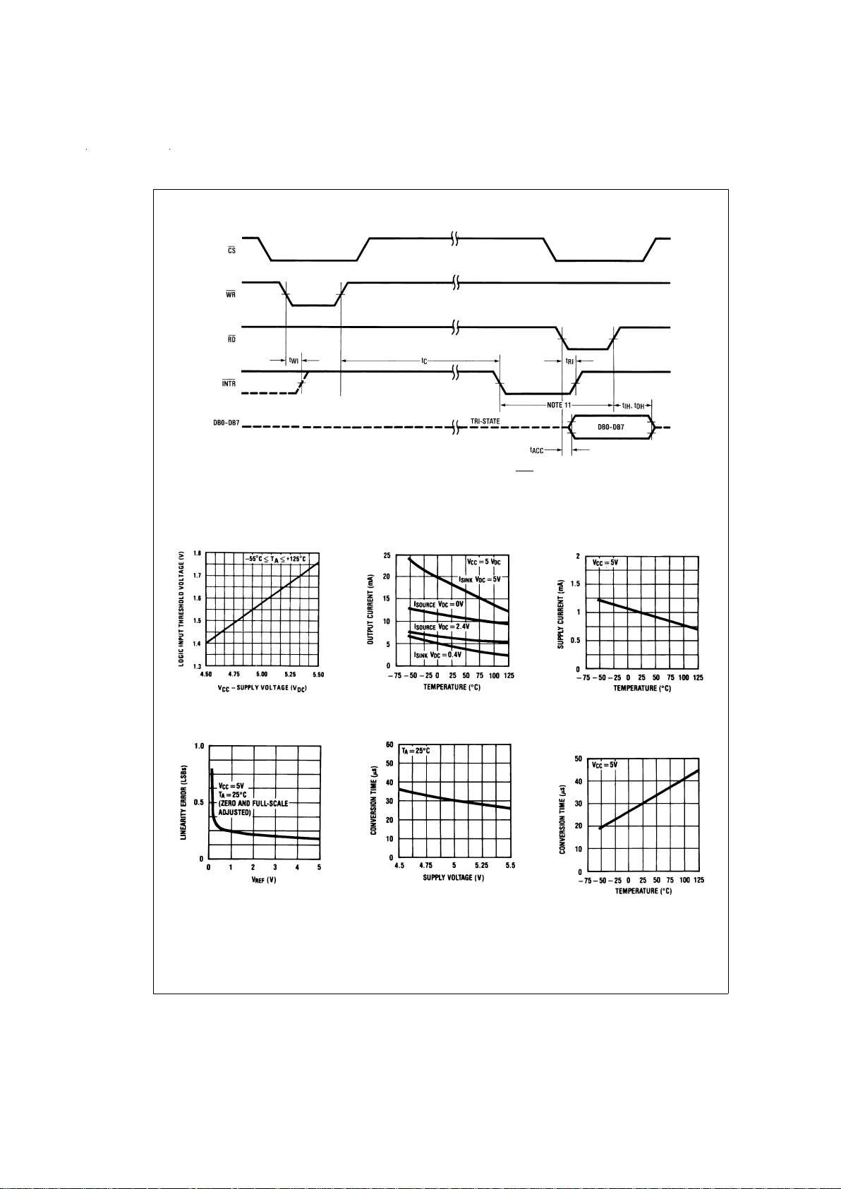
Timing Diagram
Typical Performance Characteristics
DS008557-9
Note 11: Read strobe must occur at least 600 ns after the assertion of interrupt to guarantee reset of INTR.
Logic Input Threshold
Voltage vs Supply Voltage
DS008557-23
Output Current vs
Temperature
DS008557-24
Power Supply Current vs
Temperature
DS008557-25
Linearity Error vs V
REF
DS008557-26
Conversion Time vs V
SUPPLY
DS008557-27
Conversion Time vs
Temperature
DS008557-28
www.national.com 4
Page 5
Typical Performance Characteristics (Continued)
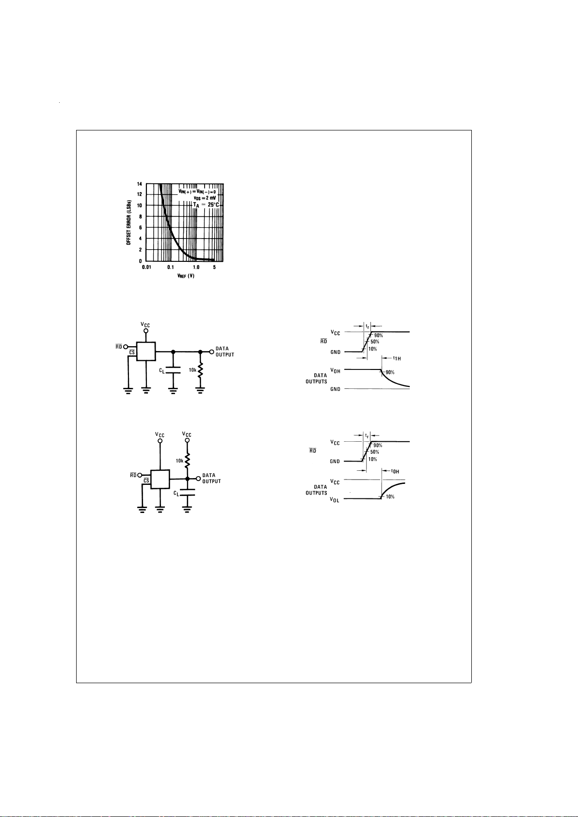
TRI-STATE Test Circuits and Waveforms
Unadjusted Offset Error vs
V
REF
Voltage
DS008557-22
t
1H
DS008557-5
t1H,C
L
=
10 pF
DS008557-6
t
r
=
20 ns
t
0H
DS008557-7
t0H,C
L
=
10 pF
DS008557-8
t
r
=
20 ns
www.national.com5
Page 6

Functional Block Diagram
DS008557-10
www.national.com 6
Page 7

Functional Description
A conversion is initiated via the CS and WR lines. If the data
from a previous conversion is not read, the INTR line will be
low.The falling edge of WR will reset the INTR line high and
ready the A/D for a conversion cycle. The rising edge of WR
starts a conversion. After the conversion cycle (tC≤ 60 µsec),
which is set by the internal clock frequency, the digital data is
transferred to the output latch and the INTR is asserted low.
Taking CS and RD low resets INTR output high and transfers
the conversion result on the output data lines (DB0–DB7).
Applications Information
1.0 REFERENCE CONSIDERATIONS
The voltage applied to the reference input of this converter
defines the voltage span of the analog input (the difference
between V
IN(MAX)
and V
IN(MIN)
) over which the 256 possible
output codes apply. The device can be used in either ratiometric applications or in systems requiring absolute accuracy. The reference pin must be connected to a voltage
source capable of driving the minimum reference input resistance of 1.1 kΩ. This pin is the top of a resistor divider string
used for the successive approximation conversion.
In a ratiometric system (
Figure 1a
), the analog input voltage
is proportional to the voltage used for the A/D reference. This
voltage is typically the system power supply, so the V
REF
pin
can be tied to V
CC
. This technique relaxes the stability requirements of the system reference as the analog input and
A/D reference move together maintaining the same output
code for a given input condition.
For absolute accuracy (
Figure 1b
), where the analog input
varies between very specific voltage limits, the reference pin
can be biased with a time and temperature stable voltage
source. The LM385 and LM336 reference diodes are good
low current devices to use with this converter.
The maximum value of the reference is limited to the V
CC
supply voltage. The minimum value, however, can be quite
small (see Typical Performance Characteristics) to allow direct conversions of transducer outputs providing less than a
5V output span. Particular care must be taken with regard to
noise pickup, circuit layout and system error voltage sources
when operating with a reduced span due to the increased
sensitivity of the converter (1 LSB equals V
REF
/256).
2.0 THE ANALOG INPUTS
2.1 Analog Differential Voltage Inputs and
Common-Mode Rejection
The differential inputs of this converter actually reduce the
effects of common-mode input noise, a signal common to
both selected “+” and “−” inputs for a conversion (60 Hz is
most typical). The time interval between sampling the “+” input and then the “−” input is
1
⁄2of a clock period. The change
in the common-mode voltage during this short time interval
can cause conversion errors. For a sinusoidal
common-mode signal this error is:
where fCMis the frequency of the common-mode signal,
Vpeak is its peak voltage value and t
C
is the conversion time.
For a 60 Hz common-mode signal to generate a
1
⁄4LSB error
(≈ 5 mV) with the converter running at 40 µS, its peak value
would have to be 5.43V. This large common-mode signal is
much greater than that generally found in a well designed
data acquisition system.
2.2 Input Current
Due to the sampling nature of the analog inputs, short duration spikes of current enter the “+” input and exit the “−” input
at the clock edges during the actual conversion. These currents decay rapidly and do not cause errors as the internal
comparator is strobed at the end of a clock period. Bypass
capacitors at the inputs will average these currents and
cause an effective DC current to flow through the output resistance of the analog signal source. Bypass capacitors
should not be used if the source resistance is greater than
1kΩ. An op amp RC active low pass filter can provide both
impedance buffering and noise filtering should a high impedance signal source be required.
3.0 OPTIONAL ADJUSTMENTS
3.1 Zero Error
The zero of theA/D does not require adjustment. If the minimum analog input voltage value, V
IN(MIN)
, is not ground, a
zero offset can be done. The converter can be made to output 0000 0000 digital code for this minimum input voltage by
biasing the V
IN
(−) input at this V
IN(MIN)
value.
The zero error of the A/D converter relates to the location of
the first riser of the transfer function and can be measured by
grounding the V
−
input and applying a small magnitude posi-
tive voltage to the V
+
input. Zero error is the difference between actual DC input voltage which is necessary to just
cause an output digital code transition from 0000 0000 to
0000 0001 and the ideal
1
⁄2LSB value (1⁄2LSB=9.8 mV for
V
REF
=
5.000 V
DC
).
3.2 Full-Scale
The full-scale adjustment can be made by applying a differential input voltage which is 1
1
⁄2LSB down from the desired
analog full-scale voltage range and then adjusting the magnitude of the V
REF
input for a digital output code changing
from 1111 1110 to 1111 1111.
3.3 Adjusting for an Arbitrary Analog Input Voltage
Range
If the analog zero voltage of the A/D is shifted away from
ground (for example, to accommodate an analog input signal
which does not go to ground), this new zero reference
should be properly adjusted first. A voltage which equals this
desired zero reference plus
1
⁄2LSB (where the LSB is calculated for the desired analog span, 1 LSB=analog span/256)
is applied to the “+” input (V
IN
(+)
) and the zero reference volt-
age at the “−” input (V
IN
(−)
) should then be adjusted to just
obtain the 00
HEX
to 01
HEX
code transition.
www.national.com7
Page 8

Applications Information (Continued)
The full-scale adjustment should be made [with the proper
V
IN
(−) voltage applied] by forcing a voltage to the VIN(+) in-
put which is given by:
where V
MAX
=
the high end of the analog input range and
V
MIN
=
the low end (the offset zero) of the analog range. (Both
are ground referenced.)
The V
REF
(or VCC) voltage is then adjusted to provide a code
change from FE
HEX
to FF
HEX
. This completes the adjust-
ment procedure.
For an example see the Zero-Shift and Span Adjust circuit
below.
DS008557-11
a) Ratiometric
DS008557-12
b) Absolute with a Reduced Span
FIGURE 1. Referencing Examples
Zero Shift and Span Adjust (2V≤V
IN
≤5V)
DS008557-13
www.national.com 8
Page 9

Applications Information (Continued)
Span Adjust 0V≤V
IN
≤3V
DS008557-14
Protecting the Input
DS008557-15
Diodes are 1N914
High Accuracy Comparator
DS008557-16
DO=all 1s if VIN(+)>VIN(−)
DO=all 0s if V
IN
(+)<VIN(−)
www.national.com9
Page 10

Applications Information (Continued)
SAMPLE PROGRAM FOR ADC0841 — INS8039 INTERFACE
CONVERTING TWO RATIOMETRIC, DIFFERENTIAL SIGNALS
ORG 0H
0000 04 10 JMP BEGIN ;START PROGRAM AT ADDR 10
ORG 10H ;MAIN PROGRAM
0010 B9 FF BEGIN: MOV R1,
#
0FFH ;LOAD R1 WITH A UNUSED ADDR
;LOCATION
0012 B8 20 MOV R0,
#
20H ;A/D DATA ADDRESS
0014 89 FF ORL P1,
#
0FFH ;SET PORT 1 OUTPUTS HIGH
0016 23 00 MOV A,00H ;LOAD THE ACC WITH 00
0018 14 50 CALL CONV ;CALL THE CONVERSION SUBROUTINE
;CONTINUE MAIN PROGRAM
Continuous Conversion
DS008557-19
Operating with Automotive Ratiometric Transducers
DS008557-17
*VIN(−)=0.15 V
CC
15%of VCC≤V
XDR
≤85%of V
CC
www.national.com 10
Page 11

Applications Information (Continued)
;CONVERSION SUBROUTINE
;ENTRY: ACC —A/D MUX DATA
;EXIT: ACC —CONVERTED DATA
ORG 50H
0050 99 FE CONV: ANL P1,
#
0FEH ;CHIP SELECT THE A/D
0052 91 MOVX
@
R1,A ;START CONVERSION
0053 09 LOOP: IN A,P1 ;INPUT INTR STATE
0054 32 53 JB1 LOOP ;IF INTR=1 GOTO LOOP
0056 81 MOVX A,@R1 ;IF INTR=0 INPUT A/D DATA
0057 89 01 ORL P1,&01H ;CLEAR THE A/D CHIP SELECT
0059 A0 MOV
@
R0,A ;STORE THE A/D DATA
005A 83 RET ;RETURN TO MAIN PROGRAM
ADC0841_INS8039 Interface
DS008557-20
www.national.com11
Page 12

Applications Information (Continued)
SAMPLE PROGRAM FOR ADC0841 — NSC800 INTERFACE
0010 NCONV EQU 16 ;TWICE THE NUMBER OF REQUIRED
;CONVERSIONS
000F DEL EQU 15 ;DELAY 60 µsec CONVERSION
001F CS EQU 1FH ;THE BOARD ADDRESS
3C00 ADDTA EQU 003CH ;START OF RAM FOR A/D
;DATA
0000' 00 DTA: DB 08H ;DATA
0001' 0E 1F START: LD C,CS
0003' 06 16 LD B,NCONV
0005' 21 0000' LD HL,DTA
0008' 11 003C LD DE,ADDTA
000B' ED A3 STCONV: OUTI ;START A CONVERSION
000D' EB EX DE,HL ;HL=RAM ADDRESS FOR THE
;A/D DATA
000E' 3E 0F LD A,DEL
0010' 3D WAIT: DEC A ;WAIT 60 µsec FOR THE
0011' C2 0013' JP NZ,WAIT ;CONVERSION TO FINISH
0014' ED A2 INI ;STORE THE A/D’S DATA
;THE REQUIRED CONVERSIONS
COMPLETED?
0016' EB EX DE,HL
0017' C2 000E' JP NZ,STCONV ;IF NOT GOTO STCONV
END
Note 12: A conversion is started, then a 60 µs wait for the A/D to complete a conversion and the data is stored at address ADDTA for the first conversion,
ADDTA+ 1 for the second conversion, etc. for a total of 8 conversions.
I/O Interface to NSC800
™
DS008557-21
www.national.com 12
Page 13

Ordering Information
Temperature Total Unadjusted Error Package
Range
±
1
⁄2LSB
±
1 LSB Outline
0˚C to +70˚C ADC0841BCN ADC0841CCN N20A Molded Dip
−40˚C to +85˚C ADC0841BCV ADC0841CCV V20A Molded Chip Carrier
www.national.com13
Page 14

14
Page 15

Physical Dimensions inches (millimeters) unless otherwise noted
Molded Dual-In-Line Package (N)
Order Number ADC0841BCN or ADC0841CCN
NS Package Number N20A
Molded Chip Carrier Package (V)
Order Number ADC0841BCV or ADC0841CCV
NS Package Number V20A
www.national.com15
Page 16

LIFE SUPPORT POLICY
NATIONAL’S PRODUCTS ARE NOT AUTHORIZED FOR USE AS CRITICAL COMPONENTS IN LIFE SUPPORT DEVICES OR SYSTEMS WITHOUT THE EXPRESS WRITTEN APPROVAL OF THE PRESIDENT OF NATIONAL SEMICONDUCTOR CORPORATION. As used herein:
1. Life support devices or systems are devices or systems which, (a) are intended for surgical implant into
the body, or (b) support or sustain life, and whose failure to perform when properly used in accordance
with instructions for use provided in the labeling, can
be reasonably expected to result in a significant injury
to the user.
2. A critical component is any component of a life support
device or system whose failure to perform can be reasonably expected to cause the failure of the life support
device or system, or to affect its safety or effectiveness.
National Semiconductor
Corporation
Americas
Tel: 1-800-272-9959
Fax: 1-800-737-7018
Email: support@nsc.com
www.national.com
National Semiconductor
Europe
Fax: +49 (0) 1 80-530 85 86
Email: europe.support@nsc.com
Deutsch Tel: +49 (0) 1 80-530 85 85
English Tel: +49 (0) 1 80-532 78 32
Français Tel: +49 (0) 1 80-532 93 58
Italiano Tel: +49 (0) 1 80-534 16 80
National Semiconductor
Asia Pacific Customer
Response Group
Tel: 65-2544466
Fax: 65-2504466
Email: sea.support@nsc.com
National Semiconductor
Japan Ltd.
Tel: 81-3-5639-7560
Fax: 81-3-5639-7507
ADC0841 8-Bit µP Compatible A/D Converter
National does not assume any responsibility for use of any circuitry described, no circuit patent licenses are implied and National reserves the right at any time without notice to change said circuitry and specifications.
 Loading...