

Datasheet ADC0838CIWMX, ADC0838CIWM, ADC0838CCWMX, ADC0838CCWM, ADC0838CCVX Datasheet (NSC)
...Page 1
ADC0831/ADC0832/ADC0834/ADC0838
8-Bit Serial I/O A/D Converters with Multiplexer Options
General Description
TheADC0831 series are 8-bit successive approximation A/D
converters with a serial I/O and configurable input multiplexers with up to 8 channels. The serial I/O is configured to
comply with the NSC MICROWIRE
™
serial data exchange
standard for easy interface to the COPS
™
family of proces-
sors, and can interface with standard shift registers or µPs.
The 2-, 4- or 8-channel multiplexers are software configured
for single-ended or differential inputs as well as channel assignment.
The differential analog voltage input allows increasing the
common-mode rejection and offsetting the analog zero input
voltage value. In addition, the voltage reference input can be
adjusted to allow encoding any smaller analog voltage span
to the full 8 bits of resolution.
Features
n NSC MICROWIRE compatible — direct interface to
COPS family processors
n Easy interface to all microprocessors, or operates
“stand-alone”
n Operates ratiometrically or with 5 V
DC
voltage
reference
n No zero or full-scale adjust required
n 2-, 4- or 8-channel multiplexer options with address logic
n Shunt regulator allows operation with high voltage
supplies
n 0V to 5V input range with single 5V power supply
n Remote operation with serial digital data link
n TTL/MOS input/output compatible
n 0.3" standard width, 8-, 14- or 20-pin DIP package
n 20 Pin Molded Chip Carrier Package (ADC0838 only)
n Surface-Mount Package
Key Specifications
n Resolution 8 Bits
n Total Unadjusted Error
±
1
⁄2LSB and±1 LSB
n Single Supply 5 V
DC
n Low Power 15 mW
n Conversion Time 32 µs
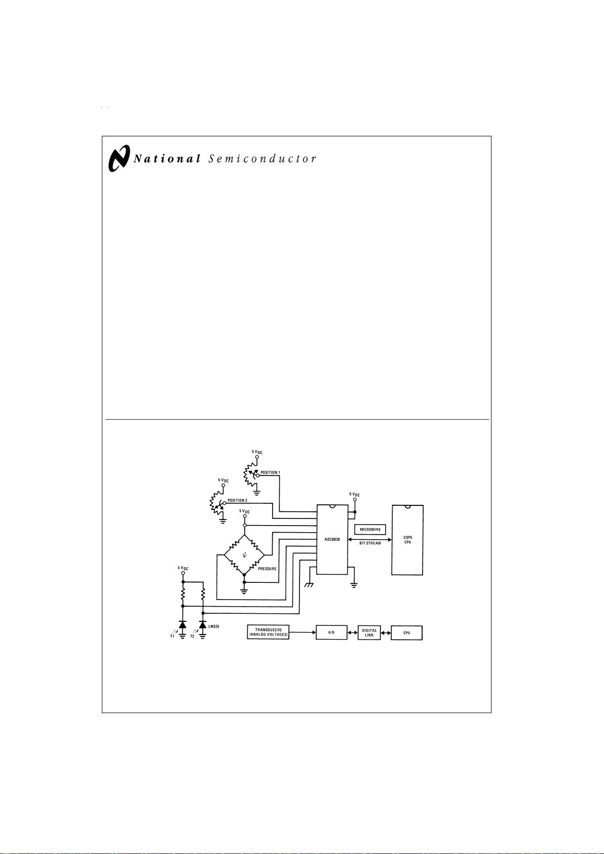
Typical Application
TRI-STATE®is a registered trademark of National Semiconductor Corporation.
COPS
™
and MICROWIRE™are trademarks of National Semiconductor Corporation.
DS005583-1
August 1999
ADC0831/ADC0832/ADC0834/ADC0838 8-Bit Serial I/O A/D Converters with Multiplexer Options
© 1999 National Semiconductor Corporation DS005583 www.national.com
Page 2
Connection Diagrams
ADC0838 8-Channel Mux
Small Outline/Dual-In-Line Package
(WM and N)
DS005583-8
Top View
ADC0834 4-Channel MUX
Small Outline/Dual-In-Line Package
(WM and N)
DS005583-30
COM internally connected to A GND
Top View
Top View
ADC0832 2-Channel MUX
Dual-In-Line Package (N)
DS005583-31
COM internally connected to GND.
V
REF
internally connected to VCC.
Top View
Top View
ADC0832 2-Channel MUX
Small Outline Package (WM)
DS005583-41
Top View
ADC0831 Single
Differential Input
Dual-In-Line Package (N)
DS005583-32
Top View
ADC0831 Single Differential Input
Small Outline Package (WM)
DS005583-42
Top View
ADC0838 8-Channel MUX
Molded Chip Carrier (PCC)
Package (V)
DS005583-33
www.national.com 2
Page 3
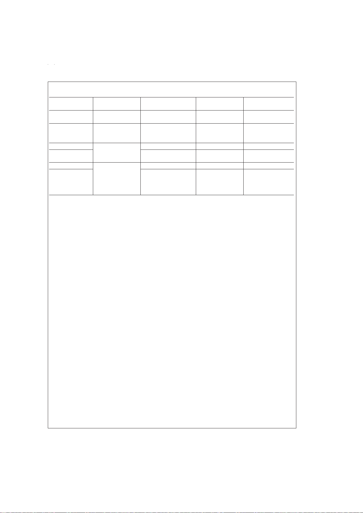
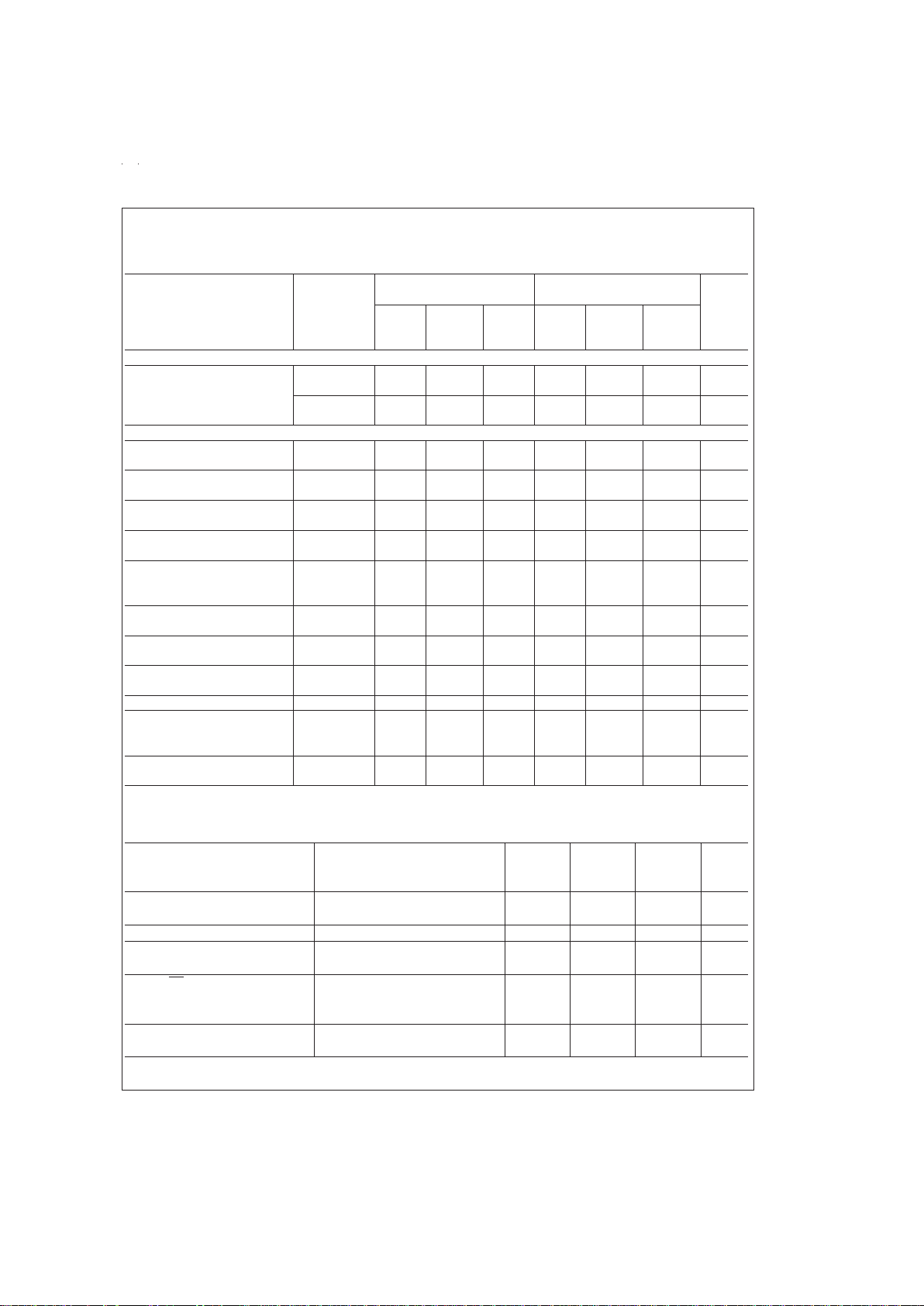
Ordering Information
Part Number Analog Input Total Package Temperature
Channels Unadjusted Error Range
ADC0831CCN 1
±
1 Molded (N) 0˚C to +70˚C
ADC0831CCWM SO(M) 0˚C to +70˚C
ADC0832CIWM 2
±
1 SO(M) −40˚C to +85˚C
ADC0832CCN Molded (N) 0˚C to +70˚C
ADC0832CCWM SO(M) 0˚C to +70˚C
ADC0834BCN 4
±
1
⁄
2
Molded (N) 0˚C to +70˚C
ADC0834CCN
±
1 Molded (N) 0˚C to +70˚C
ADC0834CCWM SO(M) 0˚C to +70˚C
ADC0838BCV 8
±
1
⁄
2
PCC (V) 0˚C to +70˚C
ADC0838CCV
±
1 PCC (V) 0˚C to +70˚C
ADC0838CCN Molded (N) 0˚C to +70˚C
ADC0838CIWM SO(M) −40˚C to +85˚C
ADC0838CCWM SO(M) 0˚C to +70˚C
See NS Package Number M14B, M20B, N08E, N14A, N20A or V20A
www.national.com3
Page 4
Absolute Maximum Ratings (Notes 1, 2)
If Military/Aerospace specified devices are required,
please contact the National Semiconductor Sales Office/
Distributors for availability and specifications.
Current into V
+
(Note 3) 15 mA
Supply Voltage, V
CC
(Note 3) 6.5V
Voltage
Logic Inputs −0.3V to V
CC
+ 0.3V
Analog Inputs −0.3V to V
CC
+ 0.3V
Input Current per Pin (Note 4)
±
5mA
Package
±
20 mA
Storage Temperature −65˚C to +150˚C
Package Dissipation
at T
A
=
25˚C (Board Mount) 0.8W
Lead Temperature (Soldering 10 sec.)
Dual-In-Line Package (Plastic) 260˚C
Molded Chip Carrier Package
Vapor Phase (60 sec.) 215˚C
Infrared (15 sec.) 220˚C
ESD Susceptibility (Note 5) 2000V
Operating Ratings (Notes 1, 2)
Supply Voltage, V
CC
4.5 VDCto 6.3 V
DC
Temperature Range T
MIN≤TA≤TMAX
ADC0832/8CIWM −40˚C to +85˚C
ADC0834BCN,
ADC0838BCV,
ADC0831/2/4/8CCN,
ADC0838CCV,
ADC0831/2/4/8CCWM 0˚C to +70˚C
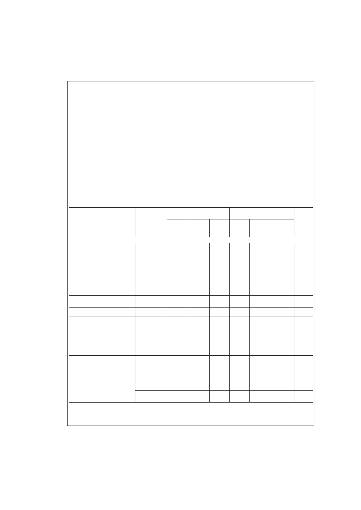
Converter and Multiplexer Electrical Characteristics The following specifications apply for
V
CC
=V+=
V
REF
=
5V, V
REF
≤ VCC+0.1V, T
A
=
T
j
=
25˚C, and f
CLK
=
250 kHz unless otherwise specified. Boldface limits
apply from T
MIN
to T
MAX
.
Parameter
Conditions CIWM Devices BCV, CCV, CCWM, BCN
and CCN Devices
Typ Tested Design Typ Tested Design Units
(Note 12) Limit Limit (Note 12) Limit Limit
(Note 13) (Note 14) (Note 13) (Note 14)
CONVERTER AND MULTIPLEXER CHARACTERISTICS
Total Unadjusted Error V
REF
=
5.00 V
ADC0838BCV (Note 6)
±
1
⁄
2
±
1
⁄
2
ADC0834BCN
±
1
⁄
2
±
1
⁄
2
LSB
(Max)
ADC0838CCV
±
1
±
1
ADC0831/2/4/8CCN
±
1
±
1
ADC0831/2/4/8CCWM
±
1
±
1
ADC0832/8CIWM
±
1
Minimum Reference 3.5 1.3 3.5 1.3 1.3 kΩ
Input Resistance (Note 7)
Maximum Reference 3.5 5.9 3.5 5.4 5.9 kΩ
Input Resistance (Note 7)
Maximum Common-Mode
Input Range (Note 8)
V
CC
+0.05 VCC+0.05 VCC+0.05 V
Minimum Common-Mode
Input Range (Note 8)
GND −0.05 GND −0.05 GND−0.05 V
DC Common-Mode Error
±
1/16
±
1
⁄
4
±
1/16
±
1
⁄
4
±
1
⁄
4
LSB
Change in zero 15 mA into V+
error from V
CC
=
5V V
CC
=
N.C.
to internal zener V
REF
=
5V
operation (Note 3) 1 1 1 LSB
V
Z
, internal MIN 15 mA into V+ 6.3 6.3 6.3
diode breakdown MAX 8.5 8.5 8.5 V
(at V
+
) (Note 3)
Power Supply Sensitivity V
CC
=
5V
±
5
%
±
1/16
±
1
⁄
4
±
1
⁄
4
±
1/16
±
1
⁄
4
±
1
⁄
4
LSB
I
OFF
, Off Channel Leakage On Channel=5V, −0.2 −0.2 −1 µA
Current (Note 9) Off Channel=0V −1
On Channel=0V, +0.2 +0.2 +1 µA
Off Channel=5V +1
www.national.com 4
Page 5
Converter and Multiplexer Electrical Characteristics The following specifications apply for
V
CC
=V+=
V
REF
=
5V, V
REF
≤ VCC+0.1V, T
A
=
T
j
=
25˚C, and f
CLK
=
250 kHz unless otherwise specified. Boldface limits
apply from T
MIN
to T
MAX
. (Continued)
Parameter
Conditions CIWM Devices BCV, CCV, CCWM, BCN
and CCN Devices
Typ Tested Design Typ Tested Design Units
(Note 12) Limit Limit (Note 12) Limit Limit
(Note 13) (Note 14) (Note 13) (Note 14)
CONVERTER AND MULTIPLEXER CHARACTERISTICS
I
ON
, On Channel Leakage On Channel=0V, −0.2 −0.2 −1 µA
Current (Note 9) Off Channel=5V −1
On Channel=5V, +0.2 +0.2 +1 µA
Off Channel=0V +1
DIGITAL AND DC CHARACTERISTICS
V
IN(1)
, Logical “1” Input V
CC
=
5.25V 2.0 2.0 2.0 V
Voltage (Min)
V
IN(0)
, Logical “0” Input V
CC
=
4.75V 0.8 0.8 0.8 V
Voltage (Max)
I
IN(1)
, Logical “1” Input V
IN
=
5.0V 0.005 1 0.005 1 1 µA
Current (Max)
I
IN(0)
, Logical “0” Input V
IN
=
0V −0.005 −1 −0.005 −1 −1 µA
Current (Max)
V
OUT(1)
, Logical “1” Output V
CC
=
4.75V
Voltage (Min) I
OUT
=
−360 µA 2.4 2.4 2.4 V
I
OUT
=
−10 µA 4.5 4.5 4.5 V
V
OUT(0)
, Logical “0” Output V
CC
=
4.75V 0.4 0.4 0.4 V
Voltage (Max) I
OUT
=
1.6 mA
I
OUT
, TRI-STATE Output V
OUT
=
0V −0.1 −3 −0.1 −3 −3 µA
Current (Max) V
OUT
=
5V 0.1 3 0.1 +3 +3 µA
I
SOURCE
, Output Source V
OUT
=
0V −14 −6.5 −14 −7.5 −6.5 mA
Current (Min)
I
SINK
, Output Sink Current (Min) V
OUT
=
V
CC
16 8.0 16 9.0 8.0 mA
I
CC
, Supply Current (Max)
ADC0831, ADC0834, 0.9 2.5 0.9 2.5 2.5 mA
ADC0838
ADC0832 Includes Ladder 2.3 6.5 2.3 6.5 6.5 mA
Current
AC Characteristics
The following specifications apply for V
CC
=
5V, t
r
=
t
f
=
20 ns and 25˚C unless otherwise specified.
Typ Tested Design Limit
Parameter Conditions (Note 12) Limit Limit Units
(Note 13) (Note 14)
f
CLK
, Clock Frequency Min 10 kHz
Max 400 kHz
t
C
, Conversion Time Not including MUX Addressing Time 8 1/f
CLK
Clock Duty Cycle Min 40
%
(Note 10) Max 60
%
t
SET-UP
, CS Falling Edge or 250 ns
Data Input Valid to CLK
Rising Edge
t
HOLD
, Data Input Valid 90 ns
after CLK Rising Edge
www.national.com5
Page 6
AC Characteristics (Continued)
The following specifications apply for V
CC
=
5V, t
r
=
t
f
=
20 ns and 25˚C unless otherwise specified.
Typ Tested Design Limit
Parameter Conditions (Note 12) Limit Limit Units
(Note 13) (Note 14)
t
pd1,tpd0
—CLK Falling C
L
=
100 pF
Edge to Output Data Valid Data MSB First 650 1500 ns
(Note 11) Data LSB First 250 600 ns
t
1H,t0H
,—Rising Edge of C
L
=
10 pF, R
L
=
10k 125 250 ns
CS to Data Output and (see TRI-STATE
®
Test Circuits)
SARS Hi–Z C
L
=
100 pf, R
L
=
2k 500 ns
C
IN
, Capacitance of Logic 5 pF
Input
C
OUT
, Capacitance of Logic 5 pF
Outputs
Note 1: Absolute Maximum Ratings indicate limits beyond which damage to the device may occur. DC and AC electrical specifications do not apply when operating
the device beyond its specified operating conditions.
Note 2: All voltages are measured with respect to the ground plugs.
Note 3: Internal zener diodes (6.3 to 8.5V) are connected from V+ to GND and V
CC
to GND. The zener at V+ can operate as a shunt regulator and is connected
to V
CC
via a conventional diode. Since the zener voltage equals the A/D’s breakdown voltage, the diode insures that VCCwill be below breakdown when the device
is powered from V+. Functionality is therefore guaranteed for V+ operation even though the resultant voltage at V
CC
may exceed the specified Absolute Max of 6.5V.
It is recommended that a resistor be used to limit the max current into V+. (See
Figure 3
in Functional Description Section 6.0)
Note 4: When the input voltage (V
IN
) at any pin exceeds the power supply rails (V
IN
<
V−or V
IN
>
V+) the absolute value of current at that pin should be limited
to 5 mA or less. The 20 mA package input current limits the number of pins that can exceed the power supply boundaries witha5mAcurrent limit to four.
Note 5: Human body model, 100 pF discharged through a 1.5 kΩ resistor.
Note 6: Total unadjusted error includes offset, full-scale, linearity, and multiplexer errors.
Note 7: Cannot be tested for ADC0832.
Note 8: For V
IN
(−)≥VIN(+) the digital output code will be 0000 0000. Twoon-chipdiodesaretiedtoeachanaloginput(seeBlockDiagram)whichwillforwardconduct
for analog input voltages one diode drop below ground or one diode drop greater than the V
CC
supply. Be careful, during testing at low VCClevels (4.5V), as high
level analog inputs (5V) can cause this input diode to conduct — especially at elevated temperatures, and cause errors for analog inputs near full-scale. The spec
allows 50 mV forward bias of either diode. This means that as long as the analog V
IN
or V
REF
does not exceed the supply voltage by more than 50 mV, the output
code will be correct. Toachieveanabsolute0V
DC
to5VDCinput voltage range will therefore require a minimum supply voltage of 4.950 VDCover temperature varia-
tions, initial tolerance and loading.
Note 9: Leakage current is measured with the clock not switching.
Note 10: A40%to 60%clock duty cycle range insures proper operation at all clock frequencies. In the case that an available clock has a duty cycle outside of these
limits, the minimum, time the clock is high or the minimum time the clock is low must be at least 1 µs. The maximum time the clock can be high is 60 µs. The clock
can be stopped when low so long as the analog input voltage remains stable.
Note 11: Since data, MSB first, is the output of the comparator used in the successive approximation loop, an additional delay is built in (see Block Diagram) to allow
for comparator response time.
Note 12: Typicals are at 25˚C and represent most likely parametric norm.
Note 13: Tested limits are guaranteed to National’s AOQL (Average Outgoing Quality Level).
Note 14: Guaranteed but not 100%production tested. These limits are not used to calculate outgoing quality levels.
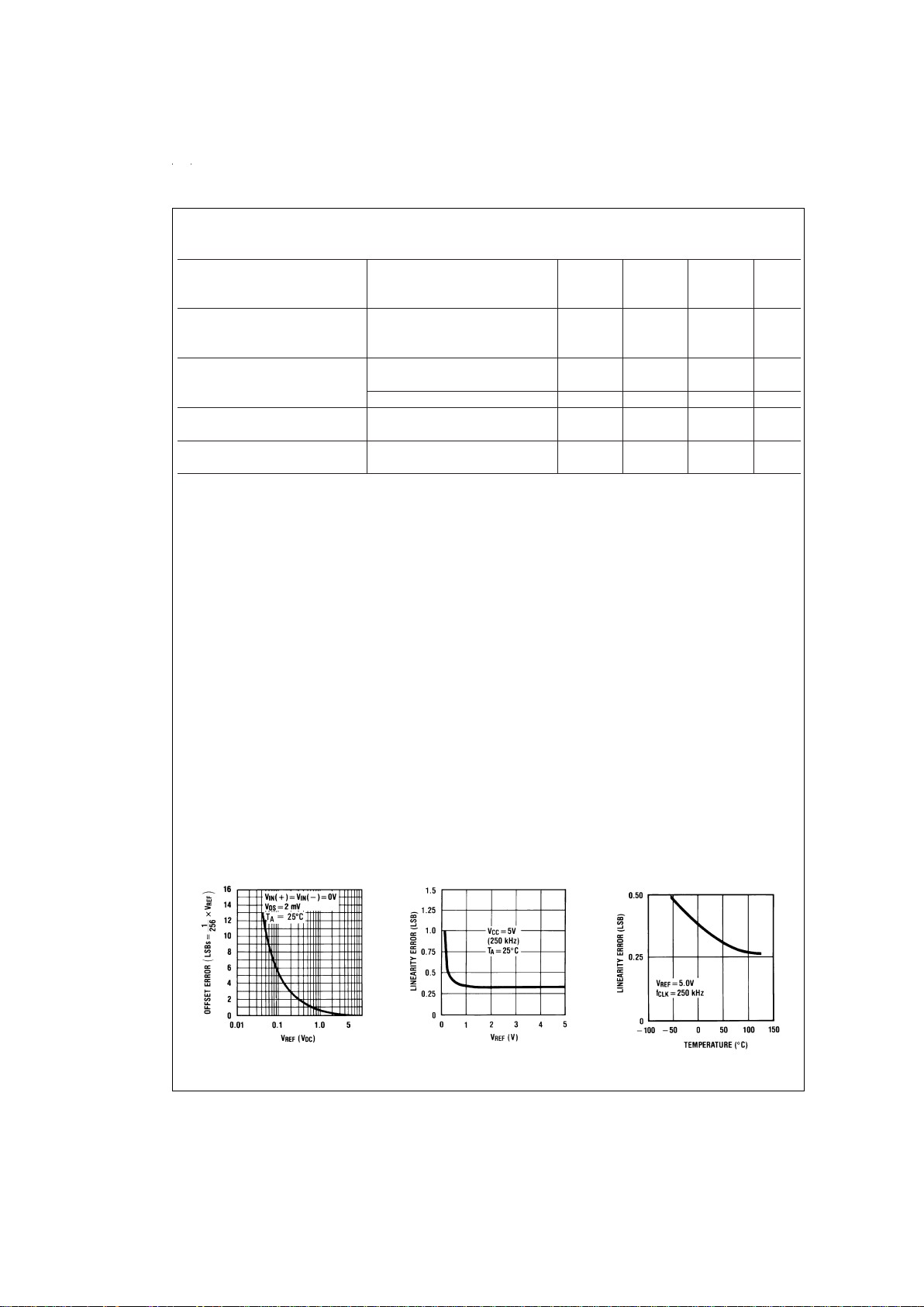
Typical Performance Characteristics
Unadjusted Offset Error
vs V
REF
Voltage
DS005583-43
Linearity Error vs V
REF
Voltage
DS005583-44
Linearity Error vs
Temperature
DS005583-45
www.national.com 6
Page 7
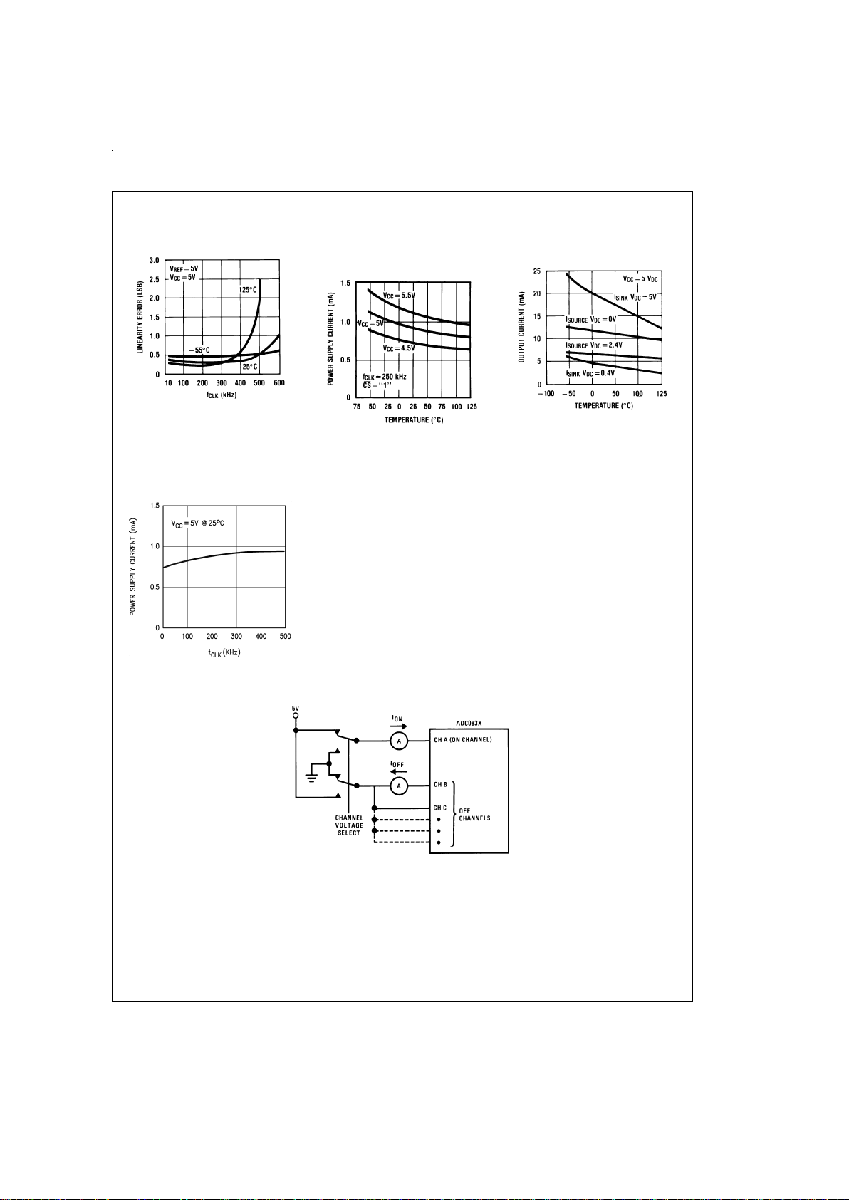
Typical Performance Characteristics (Continued)
Leakage Current Test Circuit
Linearity Error vs f
CLK
DS005583-46
Power Supply Current vs
Temperature (ADC0838,
ADC0831, ADC0834)
DS005583-47
Note: For ADC0832 add I
REF
.
Output Current vs
Temperature
DS005583-48
Power Supply Current
vs f
CLK
DS005583-29
DS005583-3
www.national.com7
Page 8
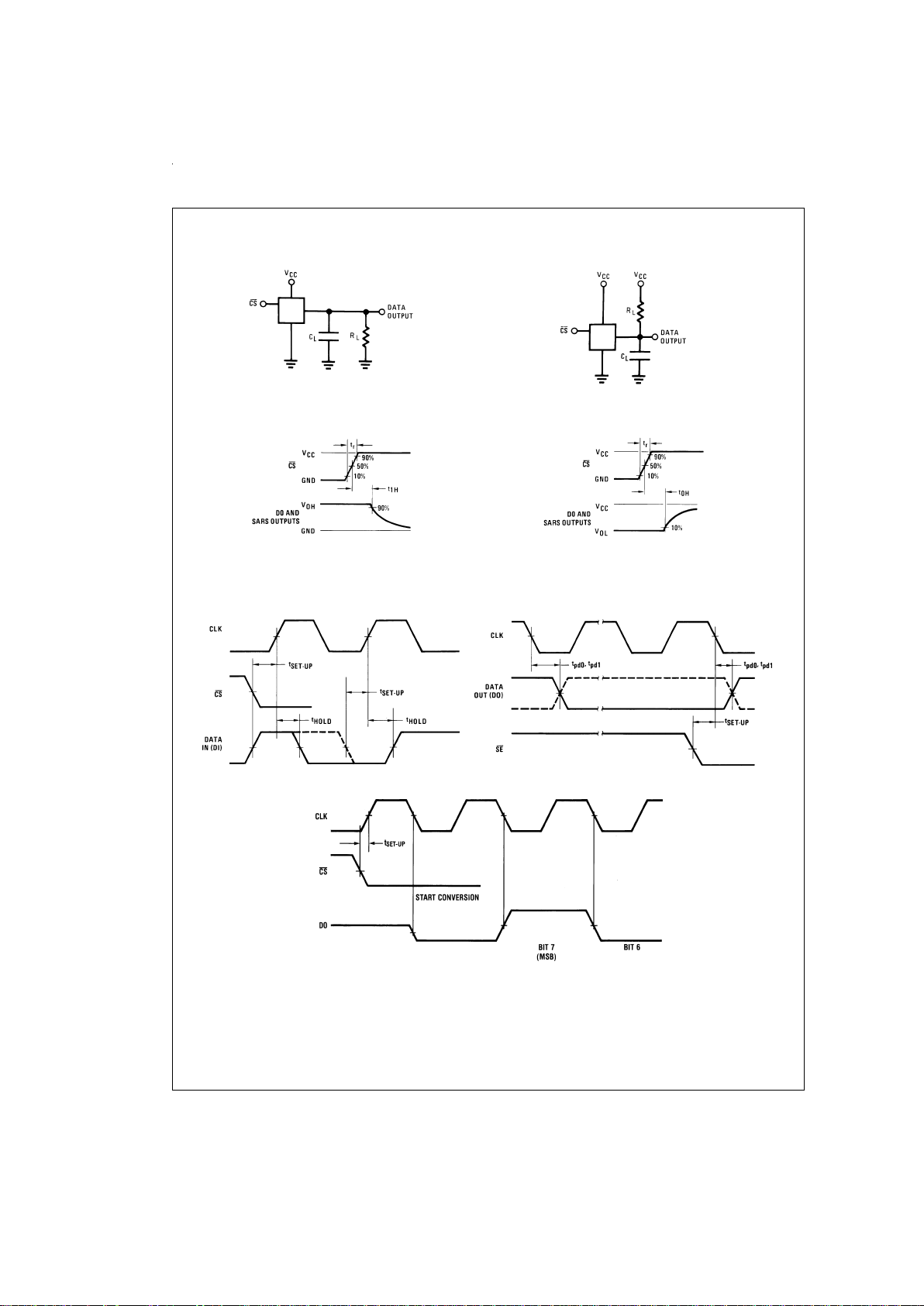
TRI-STATE Test Circuits and Waveforms
Timing Diagrams
t
1H
DS005583-49
t
0H
DS005583-50
t
1H
DS005583-51
t
0H
DS005583-52
Data Input Timing
DS005583-24
Data Output Timing
DS005583-25
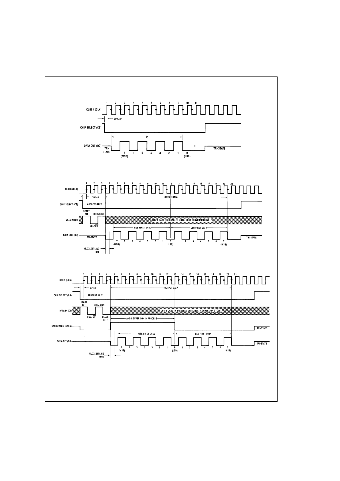
ADC0831 Start Conversion Timing
DS005583-26
www.national.com 8
Page 9
Timing Diagrams (Continued)
ADC0831 Timing
DS005583-27
*LSB first output not available on ADC0831.
ADC0832 Timing
DS005583-28
ADC0834 Timing
DS005583-5
www.national.com9
Page 10
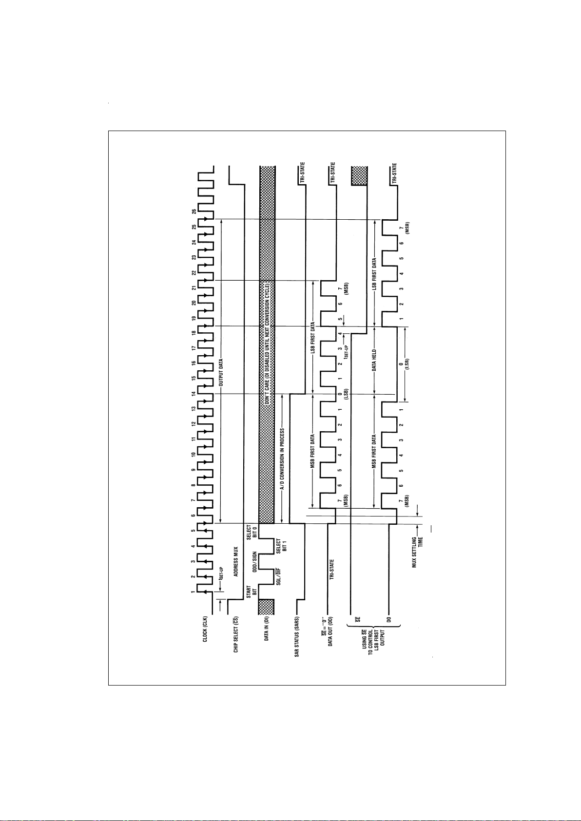
Timing Diagrams (Continued)
ADC0838 Timing
DS005583-6
*Make sure clock edge
#
18 clocks in the LSB before SE is taken low
www.national.com 10
Page 11

ADC0838 Functional Block Diagram
DS005583-7
*Some of these functions/pins are not available with other options.
Note 1: For the ADC0834, D1 is input directly to the D input of SELECT 1. SELECT 0 is forced to a “1”. For the ADC0832, DI is input directly to the DI input of ODD/SIGN. SELECT 0 is forced to
a “0” and SELECT 1 is forced to a “1”.
www.national.com11
Page 12

Functional Description
1.0 MULTIPLEXER ADDRESSING
The design of these converters utilizes a sample-data comparator structure which provides for a differential analog input to be converted by a successive approximation routine.
The actual voltage converted is always the difference between an assigned “+” input terminal and a “−” input terminal.
The polarity of each input terminal of the pair being converted indicates which line the converter expects to be the
most positive. If the assigned “+” input is less than the “−” input the converter responds with an all zeros output code.
A unique input multiplexing scheme has been utilized to provide multiple analog channels with software-configurable
single-ended, differential, or a new pseudo-differential option
which will convert the difference between the voltage at any
analog input and a common terminal. The analog signal conditioning required in transducer-based data acquisition systems is significantly simplified with this type of input flexibility.
One converter package can now handle ground referenced
inputs and true differential inputs as well as signals with
some arbitrary reference voltage.
A particular input configuration is assigned during the MUX
addressing sequence, prior to the start of a conversion. The
MUX address selects which of the analog inputs are to be
enabled and whether this input is single-ended or differential.
In the differential case, it also assigns the polarity of the
channels. Differential inputs are restricted to adjacent channel pairs. For example channel 0 and channel 1 may be selected as a different pair but channel 0 or 1 cannot act differentially with any other channel. In addition to selecting
differential mode the sign may also be selected. Channel 0
may be selected as the positive input and channel 1 as the
negative input or vice versa. This programmability is best illustrated by the MUX addressing codes shown in the following tables for the various product options.
The MUX address is shifted into the converter via the DI line.
Because the ADC0831 contains only one differential input
channel with a fixed polarity assignment, it does not require
addressing.
The common input line on the ADC0838 can be used as a
pseudo-differential input. In this mode, the voltage on this pin
is treated as the “−” input for any of the other input channels.
This voltage does not have to be analog ground; it can be
any reference potential which is common to all of the inputs.
This feature is most useful in single-supply application where
the analog circuitry may be biased up to a potential other
than ground and the output signals are all referred to this
potential.
TABLE 1. Multiplexer/Package Options
Part Number of Analog Channels Number of
Number Single-Ended Differential Package Pins
ADC0831 1 1 8
ADC0832 2 1 8
ADC0834 4 2 14
ADC0838 8 4 20
www.national.com 12
Page 13

Functional Description (Continued)
TABLE 2. MUX Addressing: ADC0838
Single-Ended MUX Mode
MUX Address Analog Single-Ended Channel
#
SGL/ ODD/ SELECT 01234567COM
DIF
SIGN 1 0
1000+ −
1001 + −
1010 + −
1011 + −
1100 + −
1101 + −
1110 + −
1111 +−
TABLE 3. MUX Addressing: ADC0838
Differential MUX Mode
MUX Address Analog Differential Channel-Pair
#
SGL/ ODD/ SELECT 0123
DIF
SIGN 1 0 01234567
0000+−
0001 +−
0010 +−
0011 +−
0100−+
0101 −+
0110 −+
0111 −+
TABLE 4. MUX Addressing: ADC0834
Single-Ended MUX Mode
MUX Address Channel
#
SGL/ ODD/ SELECT
DIF SIGN 1 0123
10 0+
10 1 +
11 0 +
11 1 +
COM is internally tied to A GND
TABLE 5. MUX Addressing: ADC0834
Differential MUX Mode
MUX Address Channel
#
SGL/ ODD/ SELECT
DIF SIGN 1 0123
00 0+−
00 1 +−
01 0−+
01 1 −+
www.national.com13
Page 14

Functional Description (Continued)
TABLE 6. MUX Addressing: ADC0832
Single-Ended MUX Mode
MUX Address Channel
#
SGL/ ODD/ 0 1
DIF
SIGN
10+
11 +
COM is internally tied to A GND
TABLE 7. MUX Addressing: ADC0832
Differential MUX Mode
MUX Address Channel
#
SGL/ ODD/ 0 1
DIF
SIGN
00+ −
01− +
Since the input configuration is under software control, it can
be modified, as required, at each conversion. A channel can
be treated as a single-ended, ground referenced input for
one conversion; then it can be reconfigured as part of a differential channel for another conversion.
Figure 1
illustrates
the input flexibility which can be achieved.
The analog input voltages for each channel can range from
50 mV below ground to 50 mV above V
CC
(typically 5V) with-
out degrading conversion accuracy.
2.0 THE DIGITAL INTERFACE
A most important characteristic of these converters is their
serial data link with the controlling processor. Using a serial
communication format offers two very significant system improvements; it allows more function to be included in the
converter package with no increase in package size and it
can eliminate the transmission of low level analog signals by
locating the converter right at the analog sensor; transmitting
highly noise immune digital data back to the host processor.
To understand the operation of these converters it is best to
refer to the Timing Diagrams and Functional Block Diagram
and to follow a complete conversion sequence. For clarity a
separate diagram is shown of each device.
1.Aconversion is initiated by first pulling the CS (chip select)
line low. This line must be held low for the entire conversion.
The converter is now waiting for a start bit and its MUX assignment word.
2.A clock is then generated by the processor (if not provided
continuously) and output to the A/D clock input.
www.national.com 14
Page 15

Functional Description (Continued)
3. On each rising edge of the clock the status of the data in
(DI) line is clocked into the MUX address shift register. The
start bit is the first logic “1” that appears on this line (all leading zeros are ignored). Following the start bit the converter
expects the next 2 to 4 bits to be the MUX assignment word.
4. When the start bit has been shifted into the start location
of the MUX register, the input channel has been assigned
and a conversion is about to begin. An interval of
1
⁄2clock period (where nothing happens) is automatically inserted to allow the selected MUX channel to settle. The SAR status line
goes high at this time to signal that a conversion is now in
progress and the DI line is disabled (it no longer accepts
data).
5. The data out (DO) line now comes out of TRI-STATE and
provides a leading zero for this one clock period of MUX settling time.
6. When the conversion begins, the output of the SAR comparator, which indicates whether the analog input is greater
than (high) or less than (low) each successive voltage from
the internal resistor ladder, appears at the DO line on each
falling edge of the clock. This data is the result of the conversion being shifted out (with the MSB coming first) and can be
read by the processor immediately.
7. After 8 clock periods the conversion is completed. The
SAR status line returns low to indicate this
1
⁄2clock cycle
later.
8. If the programmer prefers, the data can be provided in an
LSB first format [this makes use of the shift enable (SE) control line]. All 8 bits of the result are stored in an output shift
register.On devices which do not include the SE control line,
the data, LSB first, is automatically shifted out the DO line,
after the MSB first data stream. The DO line then goes low
and stays low until CS is returned high. On the ADC0838 the
SE line is brought out and if held high, the value of the LSB
remains valid on the DO line. When SE is forced low, the
data is then clocked out LSB first. The ADC0831 is an exception in that its data is only output in MSB first format.
9. All internal registers are cleared when the CS line is high.
If another conversion is desired, CS must make a high to low
transition followed by address information.
The DI and DO lines can be tied together and controlled
through a bidirectional processor I/O bit with one wire. This is
possible because the DI input is only “looked-at” during the
MUX addressing interval while the DO line is still in a high
impedance state.
8 Single-Ended
DS005583-53
8 Pseudo-Differential
DS005583-54
4 Differential
DS005583-55
Mixed Mode
DS005583-56
FIGURE 1. Analog Input Multiplexer Options for the ADC0838
www.national.com15
Page 16

Functional Description (Continued)
3.0 REFERENCE CONSIDERATIONS
The voltage applied to the reference input to these converters defines the voltage span of the analog input (the difference between V
IN(MAX)
and V
IN(MIN)
) over which the 256
possible output codes apply. The devices can be used in either ratiometric applications or in systems requiring absolute
accuracy.The reference pin must be connected to a voltage
source capable of driving the reference input resistance of
typically 3.5 kΩ. This pin is the top of a resistor divider string
used for the successive approximation conversion.
In a ratiometric system, the analog input voltage is proportional to the voltage used for the A/D reference. This voltage
is typically the system power supply, so the V
REF
pin can be
tied to V
CC
(done internally on the ADC0832). This technique
relaxes the stability requirements of the system reference as
the analog input and A/D reference move together maintaining the same output code for a given input condition.
For absolute accuracy, where the analog input varies between very specific voltage limits, the reference pin can be
biased with a time and temperature stable voltage source.
The LM385 and LM336 reference diodes are good low current devices to use with these converters.
The maximum value of the reference is limited to the V
CC
supply voltage. The minimum value, however, can be quite
small (see Typical Performance Characteristics) to allow direct conversions of transducer outputs providing less than a
5V output span. Particular care must be taken with regard to
noise pickup, circuit layout and system error voltage sources
when operating with a reduced span due to the increased
sensitivity of the converter (1 LSB equals V
REF
/256).
4.0 THE ANALOG INPUTS
The most important feature of these converters is that they
can be located right at the analog signal source and through
just a few wires can communicate with a controlling processor with a highly noise immune serial bit stream. This in itself
greatly minimizes circuitry to maintain analog signal accuracy which otherwise is most susceptible to noise pickup.
However, a few words are in order with regard to the analog
inputs should the input be noisy to begin with or possibly
riding on a large common-mode voltage.
The differential input of these converters actually reduces
the effects of common-mode input noise, a signal common
to both selected “+” and “−” inputs for a conversion (60 Hz is
most typical). The time interval between sampling the “+” input and then the “−” input is
1
⁄2of a clock period. The change
in the common-mode voltage during this short time interval
can cause conversion errors. For a sinusoidal
common-mode signal this error is:
where fCMis the frequency of the common-mode signal,
V
PEAK
is its peak voltage value
and f
CLK
, is the A/D clock frequency.
For a 60 Hz common-mode signal to generate a
1
⁄4LSB error
(≈5 mV) with the converter running at 250 kHz, its peak value
would have to be 6.63V which would be larger than allowed
as it exceeds the maximum analog input limits.
Due to the sampling nature of the analog inputs short spikes
of current enter the “+” input and exit the “−” input at the
clock edges during the actual conversion. These currents
decay rapidly and do not cause errors as the internal comparator is strobed at the end of a clock period. Bypass capacitors at the inputs will average these currents and cause
an effective DC current to flow through the output resistance
of the analog signal source. Bypass capacitors should not be
used if the source resistance is greater than 1 kΩ.
This source resistance limitation is important with regard to
the DC leakage currents of input multiplexer as well. The
worst-case leakage current of
±
1 µA over temperature will
createa1mVinput error witha1kΩsource resistance. An
op amp RC active low pass filter can provide both impedance buffering and noise filtering should a high impedance
signal source be required.
DS005583-57
a) Ratiometric
DS005583-58
b) Absolute with a reduced Span
FIGURE 2. Reference Examples
www.national.com 16
Page 17

Functional Description (Continued)
5.0 OPTIONAL ADJUSTMENTS
5.1 Zero Error
The zero of the A/D does not require adjustment. If the minimum analog input voltage value, V
IN(MIN)
, is not ground a
zero offset can be done. The converter can be made to output 0000 0000 digital code for this minimum input voltage by
biasing any V
IN
(−) input at this V
IN(MIN)
value. This utilizes
the differential mode operation of the A/D.
The zero error of the A/D converter relates to the location of
the first riser of the transfer function and can be measured by
grounding the V
IN
(−) input and applying a small magnitude
positive voltage to the V
IN
(+) input. Zero error is the difference between the actual DC input voltage which is necessary to just cause an output digital code transition from 0000
0000 to 0000 0001 and the ideal
1
⁄2LSB value (1⁄2LSB=9.8
mV for V
REF
=
5.000 V
DC
).
5.2 Full-Scale
The full-scale adjustment can be made by applying a differential input voltage which is 1
1
⁄2LSB down from the desired
analog full-scale voltage range and then adjusting the magnitude of the V
REF
input (or VCCfor the ADC0832) for a digi-
tal output code which is just changing from 1111 1110 to 1111
1111.
5.3 Adjusting for an Arbitrary Analog Input Voltage
Range
If the analog zero voltage of the A/D is shifted away from
ground (for example, to accommodate an analog input signal
which does not go to ground), this new zero reference
should be properly adjusted first. A V
IN
(+) voltage which
equals this desired zero reference plus
1
⁄2LSB (where the
LSB is calculated for the desired analog span, using 1 LSB
=
analog span/256) is applied to selected “+” input and the
zero reference voltage at the corresponding “−” input should
then be adjusted to just obtain the 00
HEX
to 01
HEX
code tran-
sition.
The full-scale adjustment should be made [with the proper
V
IN
(−) voltage applied] by forcing a voltage to the VIN(+) in-
put which is given by:
where:
V
MAX
=
the high end of the analog input range
and
V
MIN
=
the low end (the offset zero) of the analog
range.
(Both are ground referenced.)
The V
REF
(or VCC) voltage is then adjusted to provide a code
change from FE
HEX
to FF
HEX
. This completes the adjust-
ment procedure.
6.0 POWER SUPPLY
A unique feature of the ADC0838 and ADC0834 is the inclusion of a zener diode connected from the V
+
terminal to
ground which also connects to the V
CC
terminal (which is the
actual converter supply) through a silicon diode, as shown in
Figure 3
. (Note 3)
This zener is intended for use as a shunt voltage regulator to
eliminate the need for any additional regulating components.
This is most desirable if the converter is to be remotely located from the system power source.
Figure 4
and
Figure 5
illustrate two useful applications of this on-board zener when
an external transistor can be afforded.
An important use of the interconnecting diode between V
+
and VCCis shown in
Figure 6
and
Figure 7
. Here, this diode
is used as a rectifier to allow the V
CC
supply for the converter
to be derived from the clock. The low current requirements of
the A/D and the relatively high clock frequencies used (typically in the range of 10k–400 kHz) allows using the small
value filter capacitor shown to keep the ripple on the V
CC
line
to well under
1
⁄4of an LSB. The shunt zener regulator can
also be used in this mode. This requires a clock voltage
swing which is in excess of V
Z
.A current limit for the zener is
needed, either built into the clock generator or a resistor can
be used from the CLK pin to the V
+
pin.
DS005583-11
FIGURE 3. An On-Chip Shunt Regulator Diode
www.national.com17
Page 18

Applications
DS005583-12
FIGURE 4. Operating with a Temperature
Compensated Reference
DS005583-34
FIGURE 5. Using the A/D as
the System Supply Regulator
DS005583-35
*4.5V ≤ VCC≤ 6.3V
FIGURE 6. Generating VCCfrom the Converter Clock
DS005583-36
*4.5V ≤ VCC≤ 6.3V
FIGURE 7. Remote Sensing —
Clock and Power on 1 Wire
Digital Link and Sample Controlling Software for the
Serially Oriented COP420 and the Bit Programmable I/O INS8048
DS005583-13
www.national.com 18
Page 19

Applications (Continued)
COP CODING EXAMPLE
Mnemonic Instruction
LEI ENABLES SIO’s INPUT AND OUTPUT
SC C=1
OGI G0=0 (CS=0)
CLR A CLEARS ACCUMULATOR
AISC 1 LOADS ACCUMULATOR WITH 1
XAS EXCHANGES SIO WITH
ACCUMULATOR
AND STARTS SK CLOCK
LDD LOADS MUX ADDRESS FROM RAM
INTO ACCUMULATOR
NOP —
XAS LOADS MUX ADDRESS FROM
ACCUMULATOR TO SIO REGISTER
↑
8 INSTRUCTIONS
↓
XAS READS HIGH ORDER NIBBLE (4 BITS)
INTO ACCUMULATOR
XIS PUTS HIGH ORDER NIBBLE INTO RAM
CLR A CLEARS ACCUMULATOR
RC C=0
XAS READS LOW ORDER NIBBLE INTO
ACCUMULATOR AND STOPS SK
XIS PUTS LOW ORDER NIBBLE INTO RAM
OGI G0=1 (CS=1)
LEI DISABLES SIO’s INPUT AND OUTPUT
8048 CODING EXAMPLE
Mnemonic Instruction
START: ANL P1,
#
0F7H
;SELECT A/D (CS=0)
MOV B,#5 ;BIT COUNTER←5
MOV A,
#
ADDR
;A←MUX ADDRESS
LOOP 1: RRC A ;CY←ADDRESS BIT
JC ONE ;TEST BIT
;BIT=0
ZERO: ANL P1,
#
0FEH
;DI←0
JMP CONT ;CONTINUE
;BIT=1
ONE: ORL P1,
#
1 ;DI←1
CONT: CALL PULSE ;PULSE SK 0→1→0
DJNZ B, LOOP1;CONTINUE UNTIL
DONE
CALL PULSE ;EXTRA CLOCK FOR
SYNC
MOV B,
#
8 ;BIT COUNTER←8
LOOP 2: CALL PULSE ;PULSE SK 0→1→0
IN A, P1 ;CY←DO
RRC A
RRC A
MOV A, C ;A←RESULT
RLC A ;A(0)←BIT AND SHIFT
MOV C, A ;C←RESULT
DJNZ B, LOOP2;CONTINUE UNTIL
DONE
RETR
;PULSE SUBROUTINE
PULSE: ORL P1,
#
04 ;SK←1
NOP ;DELAY
ANL P1,
#
0FBH
;SK←0
RET
www.national.com19
Page 20

Applications (Continued)
A “Stand-Alone” Hook-Up for ADC0838 Evaluation
DS005583-59
*
Pinouts shown for ADC0838.
For all other products tie to
pin functions as shown.
Low-Cost Remote Temperature Sensor
DS005583-60
www.national.com 20
Page 21

Applications (Continued)
Digitizing a Current Flow
DS005583-15
Operating with Ratiometric Transducers
DS005583-37
*VIN(−)=0.15 V
CC
15%of VCC≤ V
XDR
≤ 85%of V
CC
www.national.com21
Page 22

Applications (Continued)
Span Adjust: 0V≤V
IN
≤3V
DS005583-61
Zero-Shift and Span Adjust: 2V≤VIN≤5V
DS005583-62
www.national.com 22
Page 23

Applications (Continued)
Obtaining Higher Resolution
DS005583-63
a) 9-Bit A/D
DS005583-64
Controller performs a routine to determine which input polarity (9-bit example) or which channel pair (10-bit example) provides a non-zero output code. This
information provides the extra bits.
b) 10-Bit A/D
www.national.com23
Page 24

Applications (Continued)
Protecting the Input
DS005583-18
Diodes are 1N914
High Accuracy Comparators
DS005583-38
DO=all 1s if +V
IN
>
−V
IN
DO=all 0s if +V
IN
<
−V
IN
www.national.com 24
Page 25

Applications (Continued)
Digital Load Cell
DS005583-19
•
Uses one more wire than load cell itself
•
Two mini-DIPs could be mounted inside load cell for digital output transducer
•
Electronic offset and gain trims relax mechanical specs for gauge factor and offset
•
Low level cell output is converted immediately for high noise immunity
4 mA-20 mA Current Loop Converter
DS005583-20
•
All power supplied by loop
•
1500V isolation at output
www.national.com25
Page 26

Applications (Continued)
Isolated Data Converter
DS005583-39
•
No power required remotely
•
1500V isolation
www.national.com 26
Page 27

Applications (Continued)
Two Wire Interface for 8 Channels
DS005583-21
www.national.com27
Page 28

Applications (Continued)
Two Wire 1-Channels Interface
DS005583-22
www.national.com 28
Page 29

Physical Dimensions inches (millimeters) unless otherwise noted
Hermetic Dual-In-Line Package (WM)
NS Package Number M14B
www.national.com29
Page 30

Physical Dimensions inches (millimeters) unless otherwise noted (Continued)
Hermetic Dual-In-Line Package (WM)
NS Package Number M20B
Molded Dual-In-Line Package (N)
NS Package Number N08E
www.national.com 30
Page 31

Physical Dimensions inches (millimeters) unless otherwise noted (Continued)
Molded Dual-In-Line Package (N)
NS Package Number N14A
Molded-Dual-In-Line Package (N)
NS Package Number N20A
www.national.com31
Page 32

Physical Dimensions inches (millimeters) unless otherwise noted (Continued)
LIFE SUPPORT POLICY
NATIONAL’S PRODUCTS ARE NOT AUTHORIZED FOR USE AS CRITICAL COMPONENTS IN LIFE SUPPORT
DEVICES OR SYSTEMS WITHOUT THE EXPRESS WRITTEN APPROVAL OF THE PRESIDENT AND GENERAL
COUNSEL OF NATIONAL SEMICONDUCTOR CORPORATION. As used herein:
1. Life support devices or systems are devices or
systems which, (a) are intended for surgical implant
into the body, or (b) support or sustain life, and
whose failure to perform when properly used in
accordance with instructions for use provided in the
labeling, can be reasonably expected to result in a
significant injury to the user.
2. A critical component is any component of a life
support device or system whose failure to perform
can be reasonably expected to cause the failure of
the life support device or system, or to affect its
safety or effectiveness.
National Semiconductor
Corporation
Americas
Tel: 1-800-272-9959
Fax: 1-800-737-7018
Email: support@nsc.com
National Semiconductor
Europe
Fax: +49 (0) 1 80-530 85 86
Email: europe.support@nsc.com
Deutsch Tel: +49 (0) 1 80-530 85 85
English Tel: +49 (0) 1 80-532 78 32
Français Tel: +49 (0) 1 80-532 93 58
Italiano Tel: +49 (0) 1 80-534 16 80
National Semiconductor
Asia Pacific Customer
Response Group
Tel: 65-2544466
Fax: 65-2504466
Email: sea.support@nsc.com
National Semiconductor
Japan Ltd.
Tel: 81-3-5639-7560
Fax: 81-3-5639-7507
www.national.com
Molded Chip Carrier Package (V)
Order Number ADC0838BCV or ADC0838CCV
NS Package Number V20A
ADC0831/ADC0832/ADC0834/ADC0838 8-Bit Serial I/O A/D Converters with Multiplexer Options
National does not assume any responsibility for use of any circuitry described, no circuit patent licenses are implied and National reserves the right at any time without notice to change said circuitry and specifications.
 Loading...