

Page 1
ADC08351
8-Bit, 42 MSPS, 40 mW A/D Converter
General Description
The ADC08351 is an easy to use low power, low cost, small
size, 42 MSPS analog-to-digital converter that digitizes signals to 8 bits. The ADC08351 uses an unique architecture
that achieves 7.2 Effective Bits with a 4.4 MHz input and
42 MHz clock frequency and 6.8 Effective Bits with a 21 MHz
input and 42 MHz clock frequency. Output formatting is
straight binary coding.
To minimize system cost and power consumption, the
ADC08351 requires minimal external components and includes input biasing to allow optional a.c. input signal coupling. The user need only provide a +3V supply and a clock.
Many applications require no separate reference or driver
components.
The excellent dc and ac characteristics of this device, together with its low powerconsumptionand+3Vsinglesupply
operation, make it ideally suited for many video and imaging
applications, including use in portable equipment. Total
power consumption is reduced to less than 7 mW in the
power-down mode. Furthermore, the ADC08351 is resistant
to latch-up and the outputs are short-circuit proof.
Fabricated on a 0.35 micron CMOS process, the ADC08351
is offered in TSSOP and LLP (a molded lead frame-based
chip-scale package), and is designed to operate over the
industrial temperature range of −40˚C to +85˚C.
Features
n Low Input Capacitance
n Internal Sample-and-Hold Function
n Single +3V Operation
n Power Down Feature
n TRI-STATE Outputs
Key Specifications
j
Resolution 8 Bits
j
Maximum Sampling Frequency 42 MSPS (min)
j
ENOB@f
CLK
= 42 MHz, fIN= 4.4 MHz 7.2 Bits (typ)
j
Guaranteed No Missing Codes
j
Power Consumption 40 mW (typ); 48 mW (max)
(Excluding Reference Current)
Applications
n Video Digitization
n Digital Still Cameras
n Set Top Boxes
n Digital Camcorders
n Communications
n Medical Imaging
n Personal Computer Video
n CCD Imaging
n Electro-Optics
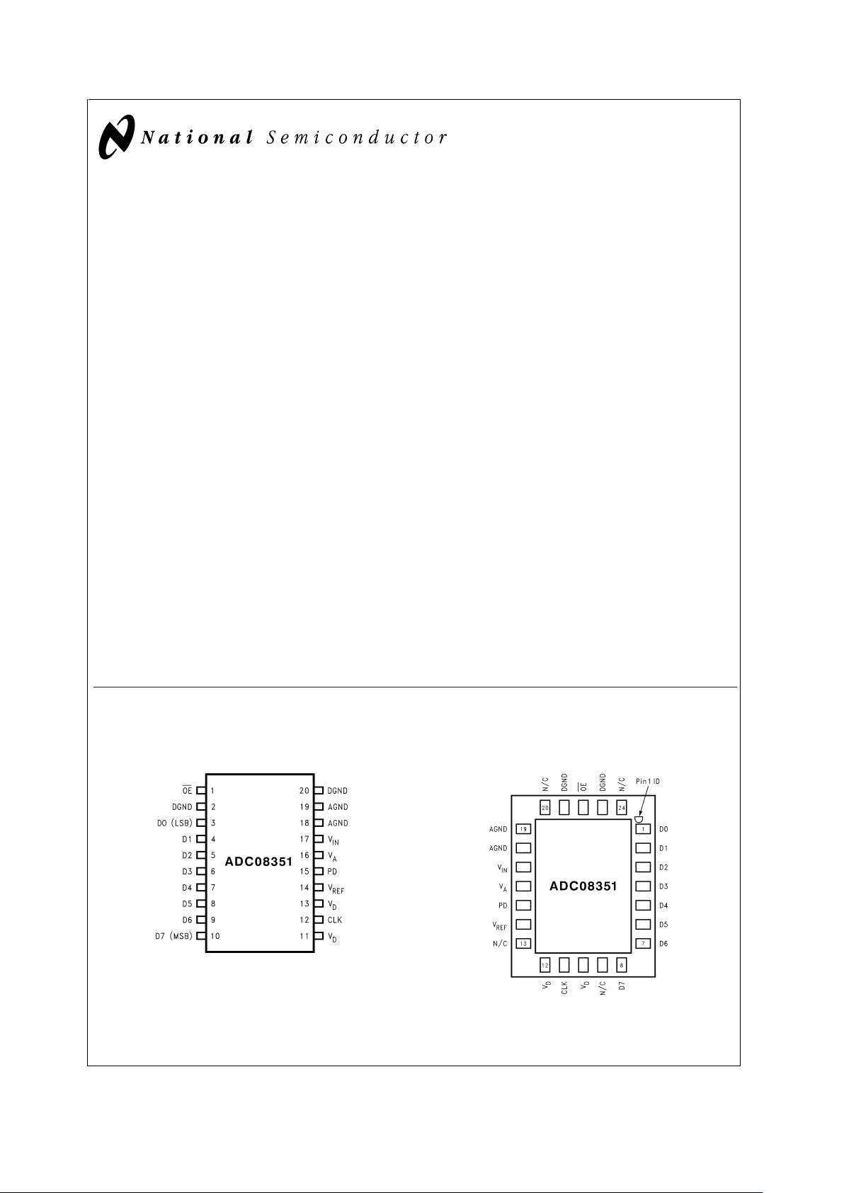
Pin Configuration
20-Pin TSSOP
DS100895-1
Top View
24-Pin LLP (CSP)
DS100895-34
Bottom View
September 2000
ADC08351 8-Bit, 42 MSPS, 40 mW A/D Converter
© 2001 National Semiconductor Corporation DS100895 www.national.com
Page 2
Ordering Information
ADC08351CIMTC TSSOP
ADC08351CIMTCX TSSOP (tape & reel)
ADC08351CILQ LLP (tape & reel - 1, 000 units)
ADC08351CILQX LLP (tape & reel - 4, 500 units)
ADC08351 Block Diagram
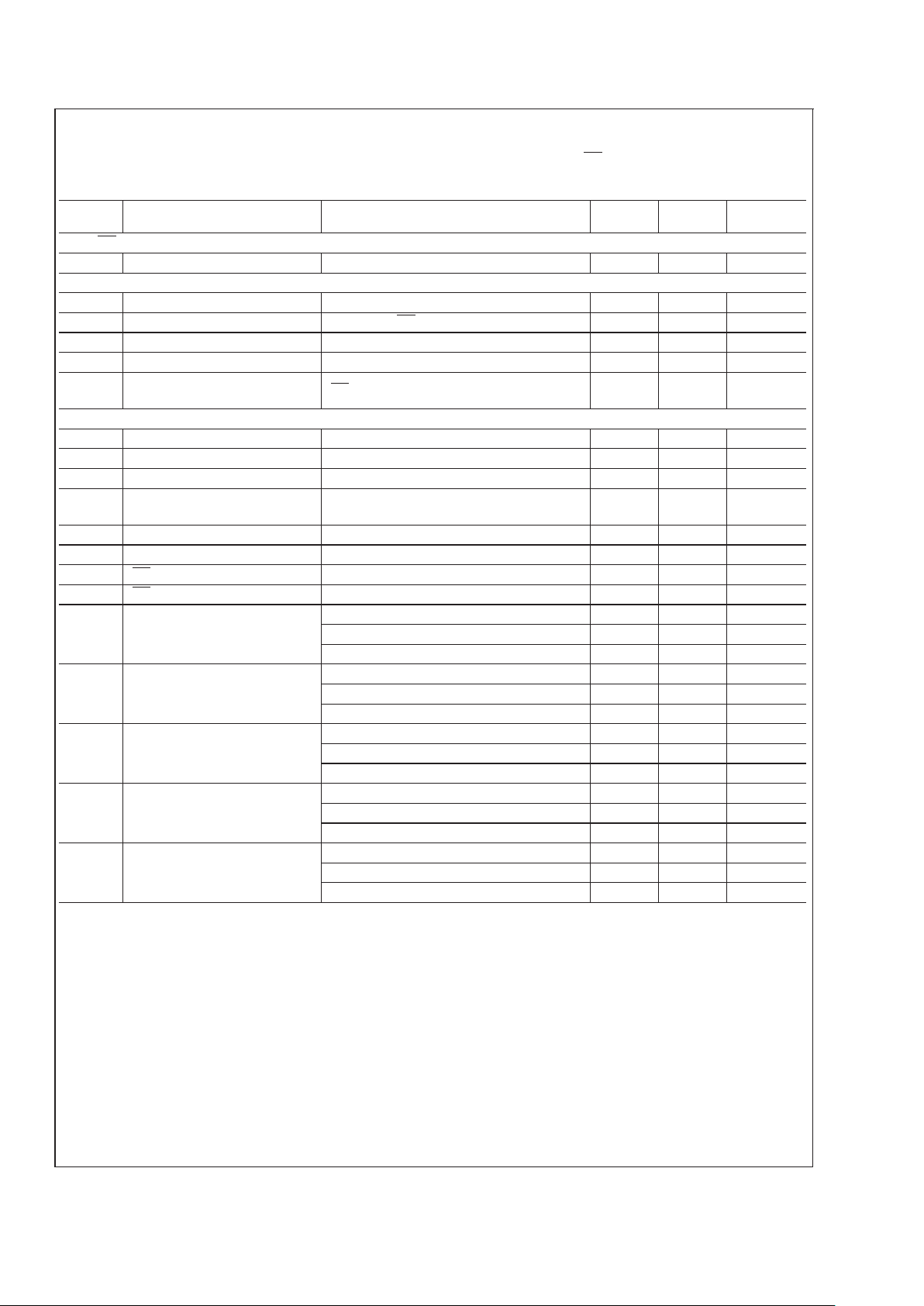
Pin Descriptions and Equivalent Circuits
(LLP pins in parentheses)
Pin
No.
Symbol Equivalent Circuit Description
17
(17)
V
IN
Analog signal input. Conversion range is 0.5 V
P-P
to
0.68 V
A
.
14
(14)
V
REF
Positive reference voltage input. Operating range of
this voltage is 0.75V to V
A
. This pin should be
bypassed with a 10 µF tantalum or aluminum
electrolytic capacitor and a 0.1 µF ceramic chip
capacitor.
1
(22)
OE
CMOS/TTL compatible digital input that, when low,
enables the digital outputs of the ADC08351. When
high, the outputs are in a high impedance state.
12
(11)
CLK
CMOS/TTL compatible digital clock input. V
IN
is
sampled on the falling edge of CLK input.
15
(15)
PD
CMOS/TTL compatible digital input that, when high,
puts the ADC08351 into the power down mode,
where it consumes minimal power. When this pin is
low, the ADC08351 is in the normal operating
mode.
DS100895-2
ADC08351
www.national.com 2
Page 3
Pin Descriptions and Equivalent Circuits (LLP pins in parentheses) (Continued)
Pin
No.
Symbol Equivalent Circuit Description
3 thru
10
(1 thru
8)
D0–D7
Conversion data digital output pins. D0 is the LSB,
D7 is the MSB. Valid data is output just after the
rising edge of the CLK input. These pins are
enabled by bringing the OE pin low.
11, 13
(10,
12)
V
D
Positive digital supply pin. Connect to a clean, quiet
voltage source of +3V. V
A
and VDshould have a
common supply and be separately bypassed with a
10 µF tantalum or aluminum electrolytic capacitor
and a 0.1 µF ceramic chip capacitor. See Section
3.0 for more information.
2, 20
(21,
23)
DGND
The ground return for the digital supply. AGND and
DGND should be connected together close to the
ADC08351.
16
(16)
V
A
Positive analog supply pin. Connected to a clean,
quiet voltage source of +3V. V
A
and VDshould have
a common supply and be separately bypassed with
a 10 µF tantalum or aluminum electrolytic capacitor
and a 0.1 µF ceramic chip capacitor. See Section
3.0 for more information.
18, 19
(18,
19)
AGND
The ground return for the analog supply. AGND and
DGND should be connected together close to the
ADC08351 package.
ADC08351
www.national.com3
Page 4
Absolute Maximum Ratings (Notes 1, 2)
If Military/Aerospace specified devices are required,
please contact the National Semiconductor Sales Office/
Distributors for availability and specifications.
Supply Voltage (V
A,VD
) 4.2V
Voltage on Any Input or
Output Pin −0.3V to 4.2V
Ground Difference
(AGND–DGND)
±
100 mV
CLK, OE Voltage Range
−0.5 to (VA+ 0.5V)
Digital Output Voltage (V
OH,VOL
)V
D
to DGND
Input Current at Any Pin (Note 3)
±
25 mA
Package Input Current (Note 3)
±
50 mA
Package Dissipation at T
A
= 25˚C (Note 4)
ESD Susceptibility (Note 5)
Human Body Model 4000V
Machine Model 200V
Soldering Temp., Infrared, 10 sec. (Note 6) 235˚C
Storage Temperature −65˚C to +150˚C
Operating Ratings (Notes 1, 2)
Operating Temperature Range −40˚C T
A
≤ +85˚C
Supply Voltage (V
A,VD
) +2.7V to +3.6V
Ground Difference
|DGND–AGND| 0V to 100 mV
V
IN
Voltage Range (V
P-P
) 0.5V to 0.68 V
A
Converter Electrical Characteristics
The following specifications apply for VA=VD= +3.0 VDC,V
REF
= 2.4V, VIN= 1.63 V
P-P
, OE = 0V, CL= 20 pF,
f
CLK
= 42 MHz, 50% duty cycle, unless otherwise specified.
Boldface limits apply for T
A=TMIN
to T
MAX
: all other limits TA= 25˚C (Notes 7, 8)
Symbol Parameter Conditions
Typical
(Note 9)
Limits
(Note 9)
Units
(Limits)
DC Accuracy
INL Integral Non Linearity Error
±
0.7
±
1.4 LSB (max)
DNL Differential Non Linearity
±
0.6
+1.3 LSB (max)
−1.0 LSB (min)
Missing Codes 0 (max)
E
Z
Zero Scale Offset Error −17 mV
E
FS
Full Scale Offset Error −7 mV
Video Accuracy
DP Differential Phase Error f
CLK
= 20 MHz, Video Ramp Input 1.0 Degree
DG Differential Gain Error f
CLK
= 20 MHz, Video Ramp Input 1.5 %
Analog Input and Reference Characteristics
C
IN
VINInput Capacitance VIN= 1.5V + 0.7 Vrms
(CLK LOW) 4 pF
(CLK HIGH) 11 pF
R
IN
RINInput Resistance 7.2 kΩ
FPBW Full-Power Bandwidth 120 MHz
V
REF
Reference Input Voltage At pin 14
0.735 V
V
A
V
I
REF
Reference Input Current 7.7 mA
Power Supply Characteristics
I
A
Analog Supply Current
PD = Low 10.5 mA
PD = High 1 mA
I
D
Digital Supply Current
PD = Low, No Digital Output Load 2.9 mA
PD = High 0.5 mA
Total Operating Current Excluding Reference Current, V
IN
=0V
DC
13.4 16 mA (max)
Power Consumption (active) PD = Low (excluding reference current) 40.2 48 mW (max)
Power Consumption (power
down)
PD = High (excluding reference current)
<
7mW
CLK, OE Digital Input Characteristics
V
IH
Logical High Input Voltage VD=VA=3V 2.0 V (min)
V
IL
Logical Low Input Voltage VD=VA=3V 1.0 V (max)
I
IH
Logical High Input Current VIH=VD=VA= 3.3V 10 µA
I
IL
Logic Low Input Current VIL= 0V, VD=VA= 3.3V −10 µA
ADC08351
www.national.com 4
Page 5
Converter Electrical Characteristics (Continued)
The following specifications apply for VA=VD= +3.0 VDC,V
REF
= 2.4V, VIN= 1.63 V
P-P
, OE = 0V, CL= 20 pF,
f
CLK
= 42 MHz, 50% duty cycle, unless otherwise specified.
Boldface limits apply for T
A=TMIN
to T
MAX
: all other limits TA= 25˚C (Notes 7, 8)
Symbol Parameter Conditions
Typical
(Note 9)
Limits
(Note 9)
Units
(Limits)
CLK, OE Digital Input Characteristics
C
IN
Logic Input Capacitance 10 pF
Digital Output Characteristics
I
OH
High Level Output Current VD= 2.7V, VOH=VD−0.5V −1.1 mA (min)
I
OL
Low Level Output Current VD= 2.7V, OE = DGND, VOL= 0.4V 1.8 mA (min)
V
OH
High Level Output Voltage VD= 2.7V, IOH= −360 µA 2.65 V
V
OL
Low Level Output Voltage VD= 2.7V, IOL= 1.6 mA 0.2 V
I
OZH
,
I
OZL
TRI-STATE®Output Current OE = VD= 3.3V, VOH= 3.3V or VOL=0V
±
10 µA
AC Electrical Characteristics
f
C1
Maximum Conversion Rate 42 MHz (min)
f
C2
Minimum Conversion Rate 2 MHz
t
OD
Output Delay CLK High to Data Valid 14 19 ns (max)
Pipline Delay (Latency) 2.5
Clock
Cycles
t
DS
Sampling (Aperture) Delay CLK Low to Acquisition of Data 2 ns
t
OH
Output Hold Time CLK High to Data Invalid 9 ns
t
EN
OE Low to Data Valid Loaded as in
Figure 2
14 ns
t
DIS
OE High to High Z State Loaded as in
Figure 2
10 ns
ENOB Effective Number of Bits
f
CLK
= 30 MHz, fIN= 1 MHz 7.2 Bits
f
CLK
= 42 MHz, fIN= 4.4 MHz 7.2 Bits
f
CLK
= 42 MHz, fIN= 21 MHz 6.8 6.1 Bits (min)
SINAD Signal-to-Noise & Distortion
f
CLK
= 30 MHz, fIN= 1 MHz 45 dB
f
CLK
= 42 MHz, fIN= 4.4 MHz 45 dB
f
CLK
= 42 MHz, fIN= 21 MHz 43 38.5 dB (min)
SNR Signal-to-Noise Ratio
f
CLK
= 30 MHz, fIN= 1 MHz 44 dB
f
CLK
= 42 MHz, fIN= 4.4 MHz 45 dB
f
CLK
= 42 MHz, fIN= 21 MHz 44 41 dB (min)
THD Total Harmonic Distortion
f
CLK
= 30 MHz, fIN= 1 MHz −57 dB
f
CLK
= 42 MHz, fIN= 4.4 MHz −51 dB
f
CLK
= 42 MHz, fIN= 21 MHz −46 −41 dB (min)
SFDR Spurious Free Dynamic Range
f
CLK
= 30 MHz, fIN= 1 MHz 57 dB
f
CLK
= 42 MHz, fIN= 4.4 MHz 54 dB
f
CLK
= 42 MHz, fIN= 21 MHz 49 41 dB (min)
Note 1: Absolute Maximum Ratings indicate limits beyond which damage to the device may occur. Operating Ratings indicate conditions for which the device is
functional, but do not guarantee specific performance limits. For guaranteed specifications and test conditions, see the Electrical Characteristics. The guaranteed
specifications apply only for the test conditions listed. Some performance characteristics may degrade when the device is not operated under the listed test
conditions.
Note 2: All voltages are measured with respect to GND = AGND = DGND = 0V, unless otherwise specified.
Note 3: When the input voltage at any pin exceeds the power supplies (that is, less than AGND or DGND, or greater than V
A
or VD), the current at that pin should
be limited to 25 mA. The 50 mA maximum package input current rating limits the number of pinsthat can safely exceed the power supplies with an input current of
25 mA to two.
Note 4: The absolute maximum junction temperature (T
J
max) for this device is 150˚C. The maximum allowable power dissipation is dictated by TJmax, the
junction-to-ambient thermal resistance(θ
JA
), and theambient temperature (TA), and canbe calculated using the formula PDMAX=(TJmax - TA)/θJA. For the20-pin
TSSOP, θ
JA
is 135˚C/W,so PDMAX = 926 mW at25˚C and 481 mW atthe maximum operating ambient temperatureof 85˚C. Note that thepower dissipation of this
device under normal operation will typically be about 68 mW (40 mW quiescent power + 23 mW reference ladder power+5mWdueto1TTLloan on each digital
output). The values for maximum power dissipation listed above will be reached only when the ADC08351 is operated in a severe fault condition (e.g., when input
or output pins are driven beyond the power supply voltages, or the power supply polarity is reversed). Obviously, such conditions should always be avoided.
Note 5: Human body model is 100 pF capacitor discharged through a 1.5 kΩ resistor. Machine model is 220 pF discharged through ZERO Ohms.
Note 6: See AN-450, “Surface Mounting Methods and Their Effect on Product Reliability”, or the section entitled “Surface Mount” found in any post 1986 National
Semiconductor Linear Data Book, for other methods of soldering surface mount devices.
ADC08351
www.national.com5
Page 6
Converter Electrical Characteristics (Continued)
Note 7: All inputs are protected as shown below. Input voltage magnitudes up to 500 mV above the supply voltage or 500 mV below GND will not damage this
device. However, errors in the A/D conversion can occur if the input goes above V
A
or below AGND by more than 300 mV. As an example, if VAis 3.0 VDC, the
full-scale input voltage must be ≤3.3 V
DC
to ensure accurate conversions.
Note 8: To guarantee accuracy, it is required that V
A
and VDbe well bypassed. Each VAand VDpin must be decoupled with separate bypass capacitors.
Note 9: Typical figures are at T
J
= 25˚C, and represent most likely parametric norms. Test limits are guaranteed to National’s AOQL (Average Outgoing Quality
Level).
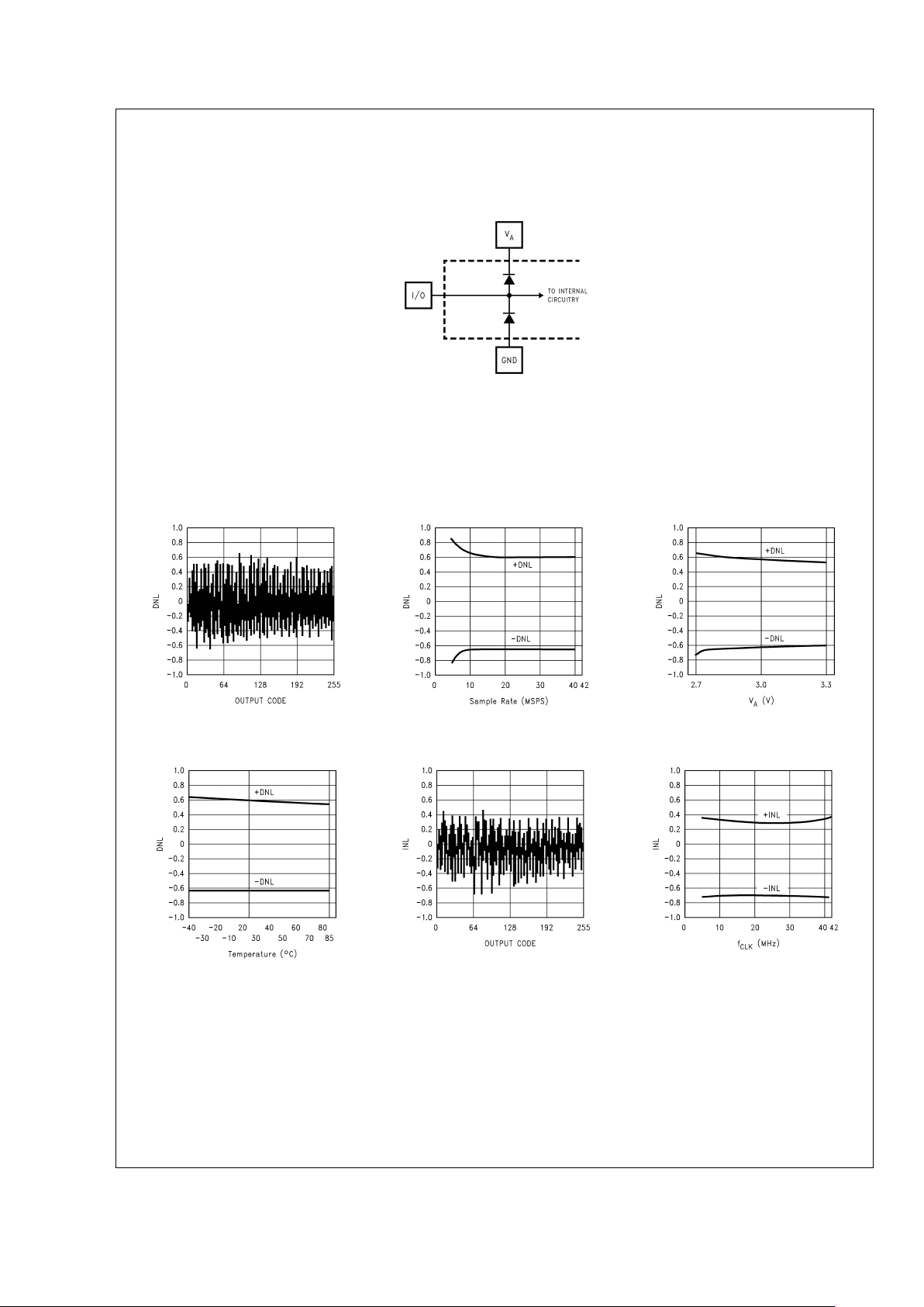
Typical Performance Characteristics V
A=VD=VD
I/O=3V,f
CLK
= 42 MHz, unless otherwise
specified
DS100895-6
DNL@42 MSPS
DS100895-7
DNL vs Sample Rate
DS100895-8
DNL vs V
A
DS100895-9
DNL vs Temperature
DS100895-10
INL@42 MSPS
DS100895-11
INL vs Sample Rate
DS100895-12
ADC08351
www.national.com 6
Page 7

Typical Performance Characteristics V
A=VD=VD
I/O = 3V, f
CLK
= 42 MHz, unless otherwise
specified (Continued)
INL vs V
A
DS100895-13
INL vs Temperature
DS100895-14
SINAD and ENOB vs f
IN
DS100895-15
SINAD and ENOB vs f
CLK
DS100895-16
SINAD and ENOB vs
Clock Duty Cycle
DS100895-17
SNR vs f
IN
DS100895-18
THD vs f
IN
DS100895-19
(ID)+(IA)vsf
CLK
DS100895-20
tODvs V
D
DS100895-21
Spectral Response@42 MSPS
DS100895-22
ADC08351
www.national.com7
Page 8

Typical Performance Characteristics V
A=VD=VD
I/O = 3V, f
CLK
= 42 MHz, unless otherwise
specified (Continued)
Specification Definitions
ANALOG INPUT BANDWIDTH is a measure of the fre-
quency at which the reconstructed output fundamental drops
3 dB below its low frequency value for a full scale input. The
test is performed with f
IN
equal to 100 kHz plus integer
multiples of f
CLK
. The input frequency at which the output is
−3 dB relative to the low frequency input signal is the full
power bandwidth.
DIFFERENTIAL GAIN ERROR is the percentage difference
between the output amplitudes of a high frequency reconstructed sine wave at two different dc input levels.
DIFFERENTIAL NON-LINEARITY (DNL) is the measure of
the maximum deviation from the ideal step size of 1 LSB.
DIFFERENTIAL PHASE ERROR is the difference in the
output phase of a reconstructed small signal sine wave at
two different dc input levels.
EFFECTIVE NUMBER OF BITS (ENOB, or EFFECTIVE
BITS) is another method of specifying Signal-to-Noise and
Distortion Ratio, or SINAD. ENOB is defined as (SINAD -
1.76)/6.02 and says that the converter is equivalent to a
perfect ADC of this (ENOB) number of bits.
FULL POWER BANDWIDTH is a measure of the frequency
at which the reconstructed output fundamental drops 3 dB
below its low frequency value for a full scale input. The test
is performed with f
IN
equal to 100KHz plus integer multiples
of f
CLK
The input frequency at which the output is —3 dB
relative to the low frequency input signal is the full power
bandwidth.
FULL SCALE OFFSET ERROR is the difference between
the analog input voltage that just causes the output code to
transition to the full scale code (all 1’s in the case of the
ADC08351) and the ideal value of 1
1
⁄2LSB below the value
of V
REF
.
INTEGRAL NON-LINEARITY (INL) is a measure of the
deviation of each individual code from a line drawn from zero
scale (
1
⁄2LSB below the first code transition) through positive
full scale (
1
⁄2LSB above the last code transition). The devia-
tion of any given code from this straight line is measured
from the center of that codevalue.Theendpointtestmethod
is used.
OUTPUT DELAY is the time delay after the rising edge of
the input clock before the data update is present at the
output pins.
OUTPUT HOLD TIME is the length of time that the output
data is valid after the rise of the input clock.
PIPELINE DELAY(LATENCY) is the number of clock cycles
between initiation of conversion and the availability of that
conversion result at the output. New data is available at
every clock cycle, but the data lags the conversion by the
pipeline delay.
SAMPLING (APERTURE) DELAY is that time required after
the fall of the clock input for the sampling switch to open.The
sample is effectively taken this amount of time after the fall of
the clock input.
SIGNAL TO NOISE RATIO (SNR) is the ratio of the rms
value of the input signal to the rms value of the other spectral
components below one-half the sampling frequency, not including harmonics or dc.
SIGNAL TO NOISE PLUS DISTORTION (S/(N+D) or
SINAD) is the ratio of the rms value of the input signal to the
rms value of all of the other spectral components below half
the clock frequency, including harmonics but excluding dc.
SPURIOUS FREE DYNAMIC RANGE (SFDR) is the difference, expressed in dB, between the rms values of the input
signal and the peak spurious signal, where a spurious signal
is any signal present in the output spectrum that is not
present at the input.
TOTAL HARMONIC DISTORTION (THD) is the ratio of the
rms total of the first six harmonic components to the rms
value of the input signal.
ZERO SCALE OFFSET ERROR is the difference between
the analog input voltage that just causes the output code to
transition to the first code and the ideal value of
1
⁄2LSB for
that transition.
ADC08351
www.national.com 8
Page 9

Timing Diagram
Functional Description
The ADC08351 achieves 6.8 effective bits at 21 MHz input
frequency with 42 MHz clock frequency digitizing to eight bits
the analog signal at V
IN
that is within the nominal voltage
range of 0.5 V
P-P
to 0.68 VA.
Input voltages below 0.0665 times the reference voltage will
cause the output word to consist of all zeroes, while input
voltages above
3
⁄4of the reference voltage will cause the
output word to consist of all ones. For example, with a V
REF
of 2.4V, input voltages below 160 mV will result in an output
word of all zeroes, while input voltages above 1.79V will
result in an output word of all ones.
The output word rate is the same as the clock frequency.
Data is acquired at the falling edge of the clock and the
digital equivalent of that data is available at the digital outputs 2.5 clock cycles plus t
OD
later. The ADC08351 will
convert as long as the clock signal is present at the CLK pin,
but the data will not appear at the outputs unless the OE pin
is low. The digital outputs are in the high impedance state
when the OE pin or when the PD pin is high.
Applications Information (All schematic
pin numbers refer to the TSSOP.)
1.0 THE ADC REFERENCE AND THE ANALOG INPUT
The capacitance seen at the input changes with the clock
level, appearing as 4 pF when the clock is low, and 11 pF
when the clock is high. Since a dynamic capacitance is more
difficult to drive than is a fixed capacitance, choose an
amplifier that can drive this type of load. The CLC409,
CLC440, LM6152, LM6154, LM6181 and LM6182 are good
devices for driving analog input of the ADC08351. Do not
drive the input beyond the supply rails.
The maximum peak-to-peak input level without clipping of
the reconstructed output is determined by the values of the
resistor string between V
REF
and AGND. The bottom of the
reference ladder has a voltage of 0.0665 times V
REF
, while
DS100895-23
FIGURE 1. ADC08351 Timing Diagram
DS100895-24
FIGURE 2. tEN,t
DIS
Test Circuit
ADC08351
www.national.com9
Page 10

Applications Information (All schematic
pin numbers refer to the TSSOP.) (Continued)
the top of the reference ladder has a voltage of 0.7468 times
V
REF
. The maximum peak-to-peak input level works out to
be about 68% of the value of V
REF
. The relationship between
the input peak-to-peak voltage and V
REF
is
We do not recommend opertaing with input levels below
1V
P-P
because the signal-to-noise ratio will degrade considerably due to the quantization noise. However, the
ADC08351 will give adequate results in many applications
with signal levels down to about 0.5 V
P-P(VREF
= 0.735V).
Very good performance can be obtained with reference voltages up to the supply voltage (V
A=VREF
= 3V, 2.04 V
P-P
).
As with all sampling ADCs, the opening and closing of the
switches associated with the sampling causes an output of
energy from the analog input, V
IN
. The reference ladder also
has switches associated with it, so the reference source
must be able to supply sufficient current to hold V
REF
steady.
The analog input of the ADC08351 is self-biased with an
18 kΩ pull-up resistor to V
REF
anda12kΩpull-down resistor
to AGND. This allows for either a.c. or d.c. coupling of the
input signal. These two resistors provide a convenient way to
ensure a signal that is less than full scale will be centered
within the input common mode range of the converter. However, the high values of these resistors and the energy
coming from this input means that performance will be improved with d.c. coupling.
The driving circuit at the signal input must be able to sink and
source sufficient current at the signal frequency to prevent
distortion from being introduced at the input.
2.0 POWER SUPPLY CONSIDERATIONS
A tantalum or aluminum electrolytic capacitor of 5 µF to
10 µF should be placed within a centimeter of each of the
A/D power pins, with a 0.1 µF ceramic chip capacitor placed
within
1
⁄2centimeter of each of the power pins. Leadless chip
capacitors are preferred because they provide lower lead
inductance than do their leaded counterparts.
While a single voltage source should be used for the analog
and digital supplies of the ADC08351, these supply pins
should be decoupled from each other to prevent any digital
noise from being coupled to the analog power pins. A ferrite
bead between the analog and digital supply pins would help
to isolate the two supplies.
The converter digital supply should not be the supply that is
used for other digital circuitry on the board. It should be the
same supply used for theA/D analog supply, decoupled from
the A/D analog supply pin, as described above. A common
analog supply should be used for both V
A
and VD, and each
of these pins should be separately bypassed with a 0.1 µF
ceramic capacitor and with low ESR a 10 µF capacitor.
As is the case with all high speed converters, theADC08351
is sensitive to power supply noise. Accordingly, the noise on
the analog supply pin should be minimized, keeping it below
200 mV
P-P
at 100 kHz. Of course, higher frequency noise on
the power supply should be even more severely limited.
No pin should ever have a voltage on it that is in excess of
the supply voltages. This can be a problem upon application
of power to a circuit. Be sure that the supplies to circuits
driving the CLK, OE, analog input and reference pins do not
come up any faster than does the voltage at the ADC08351
power pins.
3.0 LAYOUT AND GROUNDING
Proper grounding and proper routing of all signals is essential to ensure accurate conversion. Separate analog and
digital ground planes that are connected beneath the
ADC08351 are required to meet data sheet limits. The analog and digital grounds may be in the same layer,but should
be separated from each other and should never overlap
each other.
Capacitive coupling between the typically noisy digital
ground plane and the sensitive analog circuitry can lead to
poor performance that may seem impossible to isolate and
remedy. The solution is to keep the analog circuitry well
separated from the digital circuitry and from the digital
ground plane.
The back of the LLP package has a large metal area inside
the area bounded by the pins. This metal area is connected
to the die substrate (ground). This pad may be left floating if
desired. If it is connected to anything, it should be to ground
near the connection between analog and digital ground
planes. Soldering this metal pad to ground will help keep the
die cooler and could yield improved performance because of
the lower impedance between die and board grounds. However, a poor layout could compromise performance.
ADC08351
www.national.com 10
Page 11

Applications Information (All schematic pin numbers refer to the TSSOP.) (Continued)
DS100895-25
FIGURE 3. Layout examples showing separate analog and digital ground planes connected below the ADC08351.
ADC08351
www.national.com11
Page 12

Applications Information (All schematic
pin numbers refer to the TSSOP.) (Continued)
Generally,analog and digital lines should cross each other at
90 degrees to avoid getting digital noise into the analog path.
To maximize accuracy in video (high frequency) systems,
however, avoid crossing analog and digital lines altogether.
Furthermore, it is important to keep any clock lines isolated
from ALL other lines, including other digital lines. Even the
generally accepted 90 degree crossing should be avoided as
even a little coupling can cause problems at high frequencies.
Best performance at high frequencies and at high resolution
is obtained with a straight signal path. That is, the signal path
through all components should form a straight line wherever
possible.
Be especially careful with the layout of inductors. Mutual
inductance can change the characteristics of the circuit in
which they are used. Inductors should not be placed side by
side, even with just a small part of their bodies beside each
other.
The analog input should be isolated from noisy signal traces
to avoid coupling of spurious signals into the input. Any
external component (e.g., a filter capacitor) connected between the converter’s input and ground should be connected
to a very clean point in the analog ground plane.
Figure 3
gives an example of a suitable layout. All analog
circuitry (input amplifiers, filters, reference components, etc.)
should be placed on or over the analog ground plane. All
digital circuitry and I/O lines should be placed over the digital
ground plane.
All ground connections should have a low inductance path to
ground.
4.0 DYNAMIC PERFORMANCE
The ADC08351 is ac tested and its dynamic performance is
guaranteed. To meet the published specifications, the clock
source driving the CLK input must be free of jitter. For best
ac performance, isolating the ADC clock from any digital
circuitry should be done with adequate buffers, as with a
clock tree. See
Figure 4
.
It is good practice to keep the ADC clock line as short as
possible and to keep it well away from any other signals.
Other signals can introduce jitter into the clock signal. Even
lines with 90˚ crossings have capacitive coupling, so try to
avoid even these 90˚ crossings of the clock line.
Digital circuits create substantial supply and ground current
transients. The logic noise thus generated could have significant impact upon system noise performance. The best
logic family to use in systems with A/D converters is one
which employs non-saturating transistor designs, or has low
noise characteristics, such as the 74HC(T) and 74AC(T)Q
families. The worst noise generators are logic families that
draw the largest supply current transients during clock or
signal edges, like the 74F and the 74AC(T) families. In
general, slower logic families, such as 74LS and 74HC(T)
will produce less high frequency noise than do high speed
logic families, such as the 74F and 74AC(T) families.
Since digital switching transients are composed largely of
high frequency components, total ground plane copper
weight will have little effect upon the logic-generated noise.
This is because of the skin effect. Totalsurface area is more
important than is total ground plane volume.
An effective way to control ground noise is by connecting the
analog and digital ground planes together beneath the ADC
with a copper trace that is narrow compared with the rest of
the ground plane. This narrowing beneath the converter
provides a fairly high impedance to the high frequency components of the digital switching currents, directing them
away from the analog pins. The relatively lower frequency
analog ground currents do not create a significant variation
across the impedance of this relatively narrow ground connection.
5.0 TYPICAL APPLICATION CIRCUITS
Figure 5
shows a simple interface for a low impedance
source located close to the converter. As discussed in Section 1.0, the series capacitor is optional. Notice the isolation
of the ADC clock signal from the clock signals going elsewhere in the system. The reference input of this circuit is
shown connected to the 3V supply.
Video ADCs tend to have input current transients that can
upset a driving source, causing distortion of the driving signal. The resistor at the ADC08351 input isolates the amplifier’s output from the current transients at the input to the
converter.
When the signal source is not located close to the converter,
the signal should be buffered.
Figure 6
shows an example of
an appropriate buffer. The amplifier provides a gain of two to
compensate for transmission losses.
Operational amplifiers have better linearity when they operate with gain, so the input is attenuated with the 68Ω and
30Ω resistors at the non-inverting input. The 330Ω resistor in
parallel with these two resistors provides for a 75Ω cable
termination. Replacing this 330Ω resistor with one of 100Ω
will provide a 50Ω termination.
The circuit shown has anominalgainoftwo.You can provide
a gain adjustment by changing the 110Ωfeedbackresistor to
a 100Ω resistor in series with a 20Ω potentiometer.
The offset adjustment is used to bring the input signal within
the common mode range of the converter. If a fixed offset is
desired, the potentiometer and the 3.3k resistor may be
replaced with a single resistor of 3k to 4k to the appropriate
supply. The resistor value and the supply polarity used will
depend upon the amount and polarity of offset needed.
The CLC409 shown in
Figure 6
was chosen for a low cost
solution with good overall performance.
Figure 7
shows an inverting DC coupled circuit. The above
comments regarding
Figure 6
generally apply to this circuit
as well.
DS100895-26
FIGURE 4. Isolating the ADC Clock from Digital
Circuitry
ADC08351
www.national.com 12
Page 13

Applications Information (All schematic pin numbers refer to the TSSOP.) (Continued)
DS100895-27
FIGURE 5. AC Coupled Circuit for a Low Impedance Source Located Near the Converter
DS100895-28
FIGURE 6. Non-inverting Input Circuit for Remote Signal Source
ADC08351
www.national.com13
Page 14

Applications Information (All schematic pin numbers refer to the TSSOP.) (Continued)
ACCURATELY EVALUATING THE ADC
If a signal that is spectrally impure is presented to the ADC,
the output from the ADC cannot be pure. Nearly all signal
generators in use today produce signals that are not spectrally pure enough to adequately evaluate present-day
ADCs. This is especially true at higher frequencies and at
high resolutions.
To ensure that the signal you are presenting to the ADC
being evaluated is spectrally pure, use a bandpass filter
between the signal generator and the ADC input. One such
possible filter is the elliptic filter shown in Figure 8.
In addition to being used to eliminate undesired frequencies
from a desired signal, this filter can be used to filter a square
wave, reducing 3rd and higher harmonics to negligible levels.
When evaluating dynamic performance of an ADC, repeatability of measurements could be a problem unless coherent
sampling is used.
and ADC08351 evaluation system is available that can simplify evaluation of thsi product.
7.0 COMMON APPLICATION PITFALLS
Driving the inputs (analog or digital) beyond the power
supply rails. For proper operation, all inputs should not go
more than 300 mV beyond the supply rails. That is, more
than 300 mV below the ground pins or 300 mV above the
supply pins. Exceeding these limits on even a transient basis
may cause faulty or erratic operation. It is not uncommon for
high speed digital circuits (e.g., 74F and 74AC devices) to
exhibit undershoot that goes more than a volt below ground
or above the power supply. Since these conditions are of
very short duration with very fast rise and fall times, they can
DS100895-29
FIGURE 7. Inverting Circuit with Bias Adjust
DS100895-31
FIGURE 8. This elliptic filter has a cutoff frequency of about 11MHz and is suitable for input frequencies of 5MHz to
10MHz. It should be driven by a generator of 75Ω source impedance and teminated with 75Ω. This termination may
be provided by the ADC evaluation circuit.
ADC08351
www.national.com 14
Page 15

Applications Information (All schematic
pin numbers refer to the TSSOP.) (Continued)
inject noise into the system andmaybedifficulttodetectwith
an oscilloscope. A resistor of about 50Ω to 100Ω in series
with the offending digital input will usually eliminate the
problem.
Care should be taken not to overdrive the inputs of the
ADC08351 (or any device) with a device that is powered
from supplies outside the range of the ADC08351 supply.
Such practice may lead to conversion inaccuracies and even
to device damage.
Attempting to drive a high capacitance digital data bus.
The more capacitance the output drivers have to charge for
each conversion, the more instantaneous digital current is
required from V
D
and DGND. These large charging current
spikes can couple into the analog section, degrading dynamic performance. While adequate bypassing and maintaining separate analog and digital ground planes will reduce
this problem on the board, this coupling can still occur on the
ADC08351 die. Buffering the digital data outputs (with a
74ACQ541, for example) may be necessary if the data bus
to be driven is heavily loaded.
Dynamic performance can also be improved by adding series resistors at each digital output, reducing the energy
coupled back into the converter output pins by limiting the
output slew rate. A reasonable value for these resistors is
about 47Ω.
Using an inadequate amplifier to drive the analog input.
As explained in Section 2.0, the capacitance seen at the
input alternates between 4 pF and 11 pF with the clock. This
dynamic capacitance is more difficult to drive than a fixed
capacitance, so care should be taken in choosing a driving
device. The CLC409, CLC440, LM6152, LM6154, LM6181
and LM6182 are good devices for driving the ADC08351.
Also, an amplifier with insufficient gain-bandwidth may limit
the overall frequency response of the overall circuit.
Using an operational amplifier in an insufficient gain
configuration to drive the analog input. Operational am-
plifiers, while some may be unity gain stable, generally exhibit more distortion at low in-circuit gains than at higher
gains.
Using a clock source with excessive jitter, using excessively long clock signal trace, or having other signals
coupled to the clock signal trace. This will cause the
sampling interval to vary, causing excessive output noise
and a reduction in SNR performance. Simple gates with RC
timing is generally inadequate.
Not considering the timing relationships, especially t
OD
.
Timing is always important and gets more critical with higher
speeds. If the output data is latched or looked at when that
data is in transition, you may see excessive noise and
distortion of the output signal.
ADC08351
www.national.com15
Page 16

Physical Dimensions inches (millimeters) unless otherwise noted
20-Lead TSSOP
Order Number ADC08351CIMTC
NS Package Number MTC20
ADC08351
www.national.com 16
Page 17

Physical Dimensions inches (millimeters) unless otherwise noted (Continued)
LIFE SUPPORT POLICY
NATIONAL’S PRODUCTS ARE NOT AUTHORIZED FOR USE AS CRITICAL COMPONENTS IN LIFE SUPPORT
DEVICES OR SYSTEMS WITHOUT THE EXPRESS WRITTEN APPROVAL OF THE PRESIDENT AND GENERAL
COUNSEL OF NATIONAL SEMICONDUCTOR CORPORATION. As used herein:
1. Life support devices or systems are devices or
systems which, (a) are intended for surgical implant
into the body, or (b) support or sustain life, and
whose failure to perform when properly used in
accordance with instructions for use provided in the
labeling, can be reasonably expected to result in a
significant injury to the user.
2. A critical component is any component of a life
support device or system whose failure to perform
can be reasonably expected to cause the failure of
the life support device or system, or to affect its
safety or effectiveness.
National Semiconductor
Corporation
Americas
Tel: 1-800-272-9959
Fax: 1-800-737-7018
Email: support@nsc.com
National Semiconductor
Europe
Fax: +49 (0) 180-530 85 86
Email: europe.support@nsc.com
Deutsch Tel: +49 (0) 69 9508 6208
English Tel: +44 (0) 870 24 0 2171
Français Tel: +33 (0) 1 41 91 8790
National Semiconductor
Asia Pacific Customer
Response Group
Tel: 65-2544466
Fax: 65-2504466
Email: ap.support@nsc.com
National Semiconductor
Japan Ltd.
Tel: 81-3-5639-7560
Fax: 81-3-5639-7507
www.national.com
24-Lead Package LLP
Order Number ADC08351CILQX
NS Package Number LQA24A
ADC08351 8-Bit, 42 MSPS, 40 mW A/D Converter
National does not assume any responsibility for use of any circuitry described, no circuit patent licenses are implied and National reserves the right at any time without notice to change said circuitry and specifications.
 Loading...