

Page 1
ADC08060
8-Bit, 20 MSPS to 60 MSPS, 1.3 mW/MSPS A/D Converter
General Description
The ADC08060 is a low-power, 8-bit, monolithic analog-todigital converter with an on-chip track-and-hold circuit. Optimized for low cost, low power, small size and ease of use,
this product operates at conversion rates of 20 MSPS to 70
MSPS with outstanding dynamic performance over its full
operating range while consuming just 1.3 mW per MHz of
clock frequency. That’s just 78 mW of power at 60 MSPS.
Raising the PD pin puts the ADC08060 into a Power Down
mode where it consumes just 1 mW.
The unique architecture achieves 7.5 Effective Bits with
25 MHz input frequency. The excellent DC and AC characteristics of this device, together with its low power consumption and single +3V supply operation, make it ideally suited
for many imaging and communications applications, including use in portable equipment. Furthermore, the ADC08060
is resistant to latch-up and the outputs are short-circuit proof.
The top and bottom of the ADC08060’s reference ladder are
available for connections, enabling a wide range of input
possibilities. The digital outputs are TTL/CMOS compatible
with a separate output power supply pin to support interfacing with 3V or 2.5V logic. The digital inputs (CLK and PD) are
TTL/CMOS compatible.
The ADC08060 is offered in a 24-lead plastic package
(TSSOP) and is specified over the industrial temperature
range of −40˚C to +85˚C.
Features
n Single-ended input
n Internal sample-and-hold function
n Low voltage (single +3V) operation
n Small package
n Power-down feature
Key Specifications
n Resolution 8 bits
n Maximum sampling frequency 60 MSPS (min)
n DNL 0.4 LSB (typ)
n ENOB 7.5 bits (typ) at f
IN
=25MHz
n THD −60 dB (typ)
n No missing codes Guaranteed
n Power Consumption
n Operating 1.3 mW/MSPS (typ)
n Power down 1 mW (typ)
Applications
n Digital imaging systems
n Communication systems
n Portable instrumentation
n Viterbi decoders
n Set-top boxes
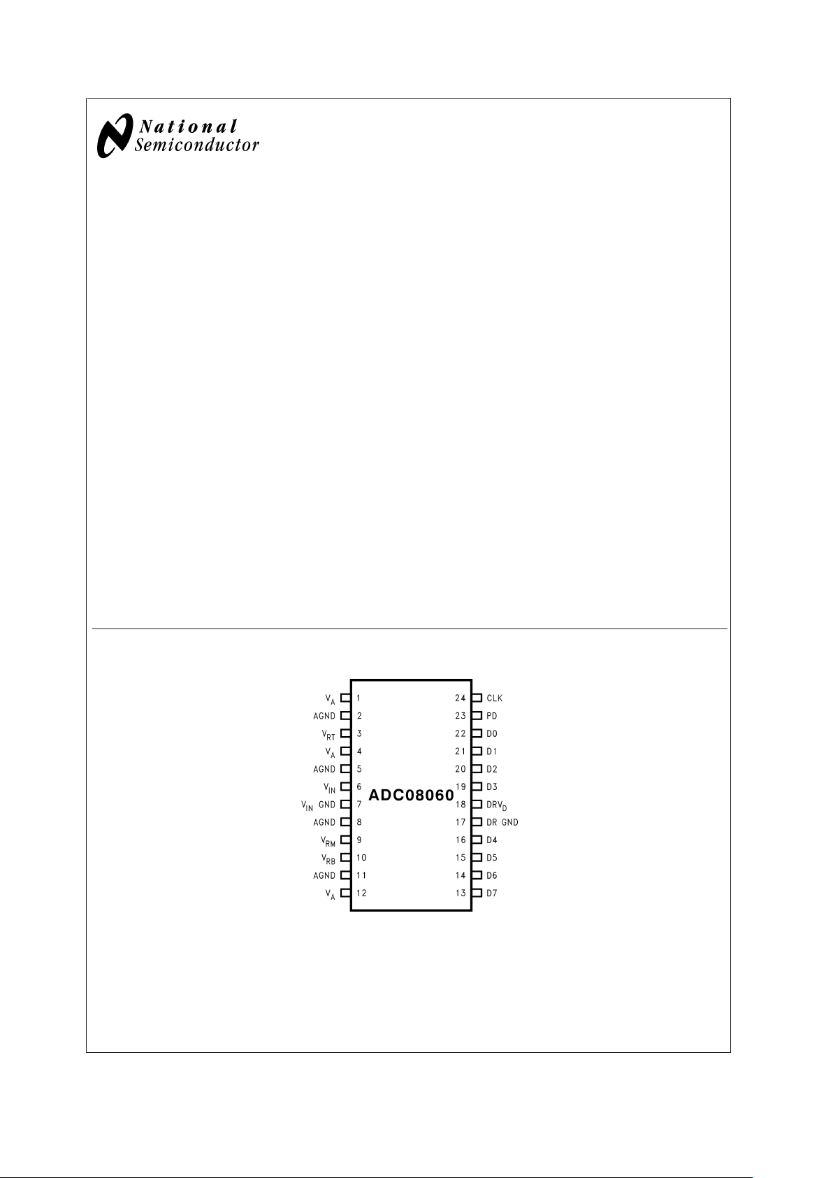
Pin Configuration
20006201
January 2003
ADC08060 8-Bit, 60 MSPS, 1.3 mW/MSPS A/D Converter
© 2003 National Semiconductor Corporation DS200062 www.national.com
Page 2
Ordering Information
ADC08060CIMT TSSOP
ADC08060CIMTX TSSOP (tape and reel)
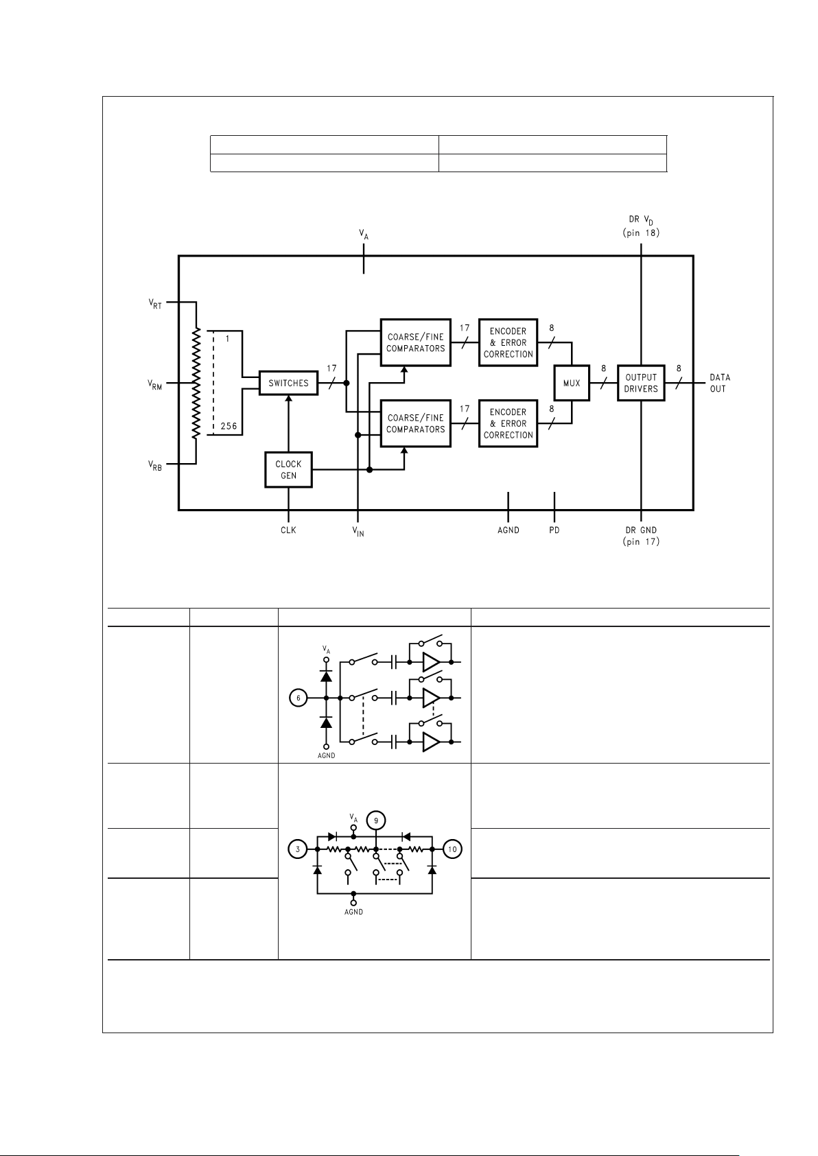
Block Diagram
20006202
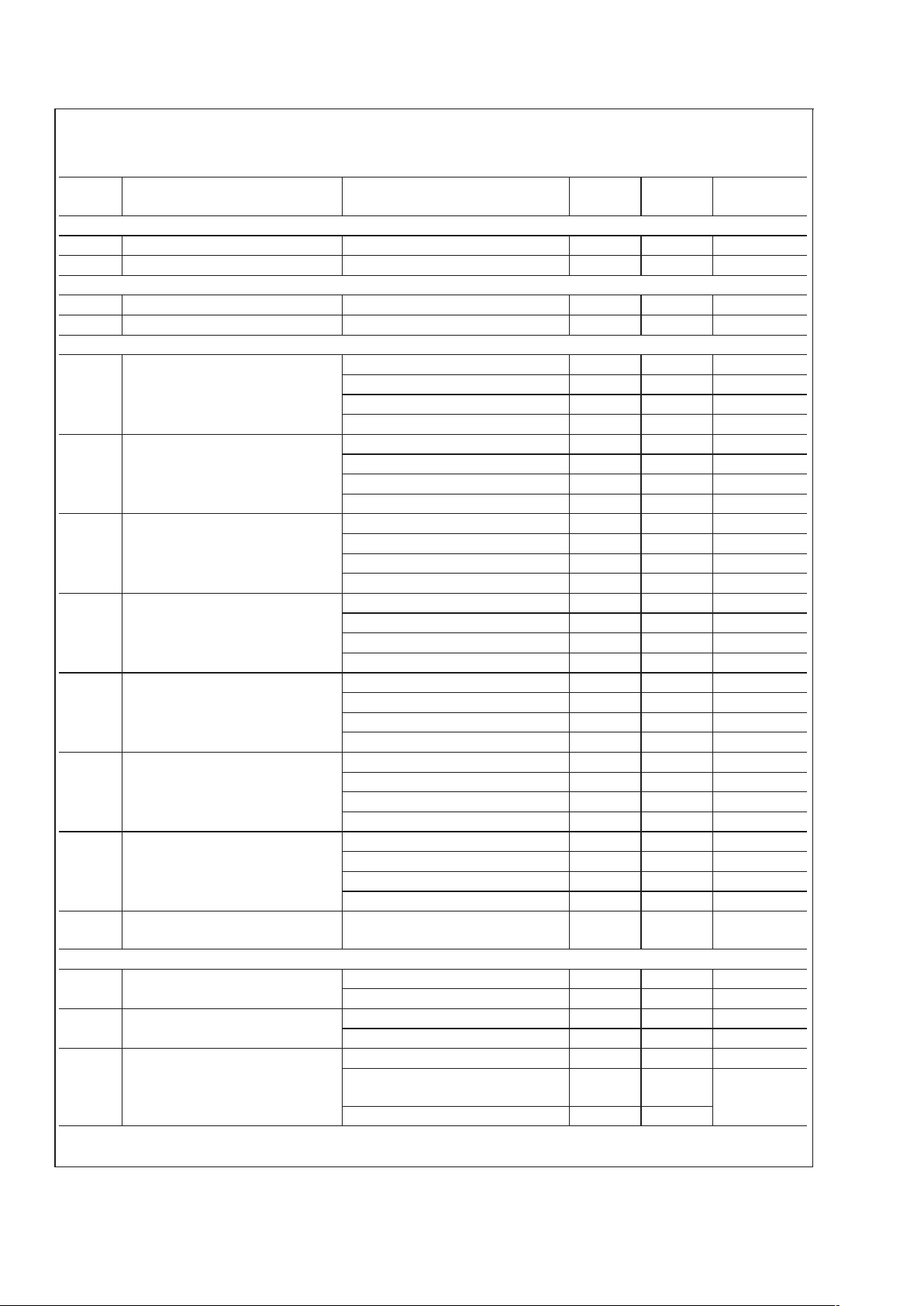
Pin Descriptions and Equivalent Circuits
Pin No. Symbol Equivalent Circuit Description
6V
IN
Analog signal input. Conversion range is VRBto VRT.
3V
RT
Analog Input that is the high (top) side of the reference
ladder of the ADC. Nominal range is 1.0V to V
A
. Voltage
on V
RT
and VRBinputs define the VINconversion range.
Bypass well. See Section 2.0 for more information.
9V
RM
Mid-point of the reference ladder. This pin should be
bypassed to a clean, quiet point in the analog ground
plane with a 0.1 µF capacitor.
10 V
RB
Analog Input that is the low side (bottom) of the
reference ladder of the ADC. Nominal range is 0.0V to
(V
RT
– 1.0V). Voltage on VRTand VRBinputs define the
V
IN
conversion range. Bypass well. See Section 2.0 for
more information.
ADC08060
www.national.com 2
Page 3
Pin Descriptions and Equivalent Circuits (Continued)
Pin No. Symbol Equivalent Circuit Description
23 PD
Power Down input. When this pin is high, the converter is
in the Power Down mode and the data output pins hold
the last conversion result.
24 CLK
CMOS/TTL compatible digital clock Input. V
IN
is sampled
on the falling edge of CLK input.
13 thru 16
and
19 thru 22
D0–D7
Conversion data digital Output pins. D0 is the LSB, D7 is
the MSB. Valid data is output just after the rising edge of
the CLK input.
7V
IN
GND Reference ground for the single-ended analog input, VIN.
1, 4, 12 V
A
Positive analog supply pin. Connect to a clean, quiet
voltage source of +3V. V
A
should be bypassed with a 0.1
µF ceramic chip capacitor for each pin, plus one
10 µF capacitor. See Section 3.0 for more information.
18 DR V
D
Power supply for the output drivers. If connected to VA,
decouple well from V
A
.
17 DR GND The ground return for the output driver supply.
2, 5, 8, 11 AGND The ground return for the analog supply.
ADC08060
www.national.com3
Page 4
Absolute Maximum Ratings (Notes 1,
2)
If Military/Aerospace specified devices are required,
please contact the National Semiconductor Sales Office/
Distributors for availability and specifications.
Supply Voltage (V
A
) 3.8V
Driver Supply Voltage (DR V
D
)V
A
+ 0.3V
Voltage on Any Input or Output Pin −0.3V to V
A
Reference Voltage (VRT,VRB)V
A
to AGND
CLK, OE Voltage Range
−0.3V to
(V
A
+ 0.3V)
Digital Output Voltage (V
OH,VOL
) DR GND to DR V
D
Input Current at Any Pin (Note 3)
±
25 mA
Package Input Current (Note 3)
±
50 mA
Power Dissipation at T
A
= 25˚C See (Note 4)
ESD Susceptibility (Note 5)
Human Body Model
Machine Model
2500V
250V
Soldering Temperature, Infrared,
10 seconds (Note 6) 235˚C
Storage Temperature −65˚C to +150˚C
Operating Ratings (Notes 1, 2)
Operating Temperature Range −40˚C ≤ T
A
≤ +85˚C
Supply Voltage (V
A
) +2.7V to +3.6V
Driver Supply Voltage (DR V
D
) +2.4V to V
A
Ground Difference |GND - DR GND| 0V to 300 mV
Upper Reference Voltage (V
RT
) 1.0V to (VA+ 0.1V)
Lower Reference Voltage (V
RB
) 0Vto(VRT− 1.0V)
V
IN
Voltage Range VRBto V
RT
Converter Electrical Characteristics
The following specifications apply for VA=DRVD= +3.0VDC,VRT= +1.9V, VRB= 0.3V, CL= 10 pF, f
CLK
= 60 MHz at 50%
duty cycle. Boldface limits apply for T
A=TMIN
to T
MAX
: all other limits TA= 25˚C (Notes 7, 8)
Symbol Parameter Conditions
Typical
(Note 9)
Limits
(Note 9)
Units
(Limits)
DC ACCURACY
INL Integral Non-Linearity
±
0.5
±
1.3 LSB (max)
DNL Differential Non-Linearity
±
0.4
+1.0
−0.9
LSB (max)
LSB (min)
Missing Codes 0 (max)
FSE Full Scale Error 18
±
28 mV (max)
ZSE Zero Scale Offset Error 26
±
35 mV (max)
ANALOG INPUT AND REFERENCE CHARACTERISTICS
V
IN
Input Voltage 1.6
V
RB
V (min)
V
RT
V (max)
C
IN
VINInput Capacitance
V
IN
= 0.75V +0.5
Vrms
(CLK LOW) 3 pF
(CLK HIGH) 4 pF
R
IN
RINInput Resistance
>
1MΩ
BW Full Power Bandwidth 200 MHz
V
RT
Top Reference Voltage 1.9
V
A
V (max)
1.0 V (min)
V
RB
Bottom Reference Voltage 0.3
V
RT
− 1.0 V (max)
0 V (min)
V
RT
-
V
RB
Reference Delta 1.6
1.0 V(min)
2.3 V(max)
R
REF
Reference Ladder Resistance VRTto V
RB
220
150 Ω (min)
300 Ω (max)
I
REF
Reference Ladder Current 7.3
5.3 mA (min)
10.6 mA (max)
CLK, PD DIGITAL INPUT CHARACTERISTICS
V
IH
Logical High Input Voltage DR VD=VA= 3.3V 2.0 V (min)
V
IL
Logical Low Input Voltage DR VD=VA= 2.7V 0.8 V (max)
I
IH
Logical High Input Current VIH=DRVD=VA= 3.3V 10 nA
ADC08060
www.national.com 4
Page 5
Converter Electrical Characteristics (Continued)
The following specifications apply for VA=DRVD= +3.0VDC,VRT= +1.9V, VRB= 0.3V, CL= 10 pF, f
CLK
= 60 MHz at 50%
duty cycle. Boldface limits apply for T
A=TMIN
to T
MAX
: all other limits TA= 25˚C (Notes 7, 8)
Symbol Parameter Conditions
Typical
(Note 9)
Limits
(Note 9)
Units
(Limits)
CLK, PD DIGITAL INPUT CHARACTERISTICS
I
IL
Logical Low Input Current VIL= 0V, DR VD=VA= 2.7V −50 nA
C
IN
Logic Input Capacitance 3 pF
DIGITAL OUTPUT CHARACTERISTICS
V
OH
High Level Output Voltage VA=DRVD= 2.7V, IOH= −400 µA 2.6 2.4 V (min)
V
OL
Low Level Output Voltage VA=DRVD= 2.7V, IOL= 1.0 mA 0.4 0.5 V (max)
DYNAMIC PERFORMANCE
ENOB Effective Number of Bits
f
IN
= 4.4 MHz, VIN= FS − 0.25 dB 7.6 Bits
f
IN
= 10 MHz, VIN= FS − 0.25 dB 7.6 7.1 Bits (min)
f
IN
= 25 MHz, VIN= FS − 0.25 dB 7.5 Bits
f
IN
= 29 MHz, VIN= FS − 0.25 dB 7.4 Bits
SINAD Signal-to-Noise & Distortion
f
IN
= 4.4 MHz, VIN= FS − 0.25 dB 47 dB
f
IN
= 10 MHz, VIN= FS − 0.25 dB 47 44.5 dB (min)
f
IN
= 25 MHz, VIN= FS − 0.25 dB 47 dB
f
IN
= 29 MHz, VIN= FS − 0.25 dB 46 dB
SNR Signal-to-Noise Ratio
f
IN
= 4.4 MHz, VIN= FS − 0.25 dB 47 dB
f
IN
= 10 MHz, VIN= FS − 0.25 dB 47 44.6 dB (min)
f
IN
= 25 MHz, VIN= FS − 0.25 dB 47 dB
f
IN
= 29 MHz, VIN= FS − 0.25 dB 46 dB
SFDR Spurious Free Dynamic Range
f
IN
= 4.4 MHz, VIN= FS − 0.25 dB 64 dBc
f
IN
= 10 MHz, VIN= FS − 0.25 dB 63 dBc
f
IN
= 25 MHz, VIN= FS − 0.25 dB 60 dBc
f
IN
= 29 MHz, VIN= FS − 0.25 dB 54 dBc
THD Total Harmonic Distortion
f
IN
= 4.4 MHz, VIN= FS − 0.25 dB −64 dBc
f
IN
= 10 MHz, VIN= FS − 0.25 dB −63 dBc
f
IN
= 25 MHz, VIN= FS − 0.25 dB -57 dBc
f
IN
= 29 MHz, VIN= FS − 0.25 dB −54 dBc
HD2 2nd Harmonic Distortion
f
IN
= 4.4 MHz, VIN= FS − 0.25 dB -70 dBc
f
IN
= 10 MHz, VIN= FS − 0.25 dB −65 dBc
f
IN
= 25 MHz, VIN= FS − 0.25 dB -64 dBc
f
IN
= 29 MHz, VIN= FS − 0.25 dB −54 dBc
HD3 3rd Harmonic Distortion
f
IN
= 4.4 MHz, VIN= FS − 0.25 dB −72 dBc
f
IN
= 10 MHz, VIN= FS − 0.25 dB −70 dBc
f
IN
= 25 MHz, VIN= FS − 0.25 dB -68 dBc
f
IN
= 29 MHz, VIN= FS − 0.25 dB −65 dBc
IMD Intermodulation Distortion
f
1
= 11 MHz, VIN= FS − 6.25 dB
f
2
= 12 MHz, VIN= FS − 6.25 dB
-55 dBc
POWER SUPPLY CHARACTERISTICS
I
A
Analog Supply Current
DC Input 25 31 mA (max)
f
IN
= 10 MHz, VIN=FS−3dB 25 mA
DR I
D
Output Driver Supply Current
DC Input 0.3 1 mA (max)
f
IN
= 10 MHz, VIN=FS−3dB 4.4 mA
I
A
+
DRI
D
Total Operating Current
DC Input 25.3 32 mA (max)
f
IN
= 10 MHz, VIN=FS−3dB,
PD = Low
29.4
mA (max)
CLK Low, PD = Hi 0.2
ADC08060
www.national.com5
Page 6
Converter Electrical Characteristics (Continued)
The following specifications apply for VA=DRVD= +3.0VDC,VRT= +1.9V, VRB= 0.3V, CL= 10 pF, f
CLK
= 60 MHz at 50%
duty cycle. Boldface limits apply for T
A=TMIN
to T
MAX
: all other limits TA= 25˚C (Notes 7, 8)
Symbol Parameter Conditions
Typical
(Note 9)
Limits
(Note 9)
Units
(Limits)
POWER SUPPLY CHARACTERISTICS
PC Power Consumption
DC Input 76 96 mW (max)
f
IN
= 10 MHz, VIN=FS−3dB,
PD = Low
88 mW
CLK Low, PD = Hi 0.6 mW
PSRR
1
Power Supply Rejection Ratio
FSE change with 2.7V to 3.3V change
in V
A
54 dB
PSRR
2
Power Supply Rejection Ratio
SNR change with 200 mV at 200 kHz
on supply
45 dB
AC ELECTRICAL CHARACTERISTICS
f
C1
Maximum Conversion Rate 70 60 MHz (min)
f
C2
Minimum Conversion Rate 20 MHz
t
CL
Minimum Clock Low Time 6.7 ns (min)
t
CH
Minimum Clock High Time 6.7 ns (min)
t
OH
Output Hold Time CLK Rise to Data Invalid 4.4 ns
t
OD
Output Delay CLK Rise to Data Valid 8.2 12 ns (max)
Pipeline Delay (Latency) 2.5 Clock Cycles
t
AD
Sampling (Aperture) Delay CLK Fall to Acquisition of Data 1.5 ns
t
AJ
Aperture Jitter 2 ps rms
Note 1: Absolute Maximum Ratings indicate limits beyond which damage to the device may occur. Operating Ratings indicate conditions for which the device is
functional, but do not guarantee specific performance limits. For guaranteed specifications and test conditions, see the Electrical Characteristics. The guaranteed
specifications apply only for the test conditions listed. Some performance characteristics may degrade when the device is not operated under the listed test
conditions.
Note 2: All voltages are measured with respect to GND = AGND = DR GND = 0V, unless otherwise specified.
Note 3: When the input voltage at any pin exceeds the power supplies (that is, less than AGND or DR GND, or greater than V
A
or DR VD), the current at that pin
should be limited to 25 mA. The 50 mA maximum package input current rating limits the number of pins that can safely exceed the power supplies with an input
current of 25 mA to two.
Note 4: The absolute maximum junction temperature (T
J
max) for this device is 150˚C. The maximum allowable power dissipation is dictated by TJmax, the
junction-to-ambient thermal resistance (θ
JA
), and the ambient temperature (TA), and can be calculated using the formula PDMAX=(TJmax − TA)/θJA. In the 24-pin
TSSOP, θ
JA
is 92˚C/W, so PDMAX = 1,358 mW at 25˚C and 435 mW at the maximum operating ambient temperature of 85˚C. Note that the power consumption of
this device under normal operation will typically be about 180 mW (88 mW quiescent power +12 mW reference ladder power). The values for maximum power
dissipation listed above will be reached only when the ADC08060 is operated in a severe fault condition (e.g., when input or output pins are driven beyond the power
supply voltages, or the power supply polarity is reversed). Obviously, such conditions should always be avoided.
Note 5: Human body model is 100 pF capacitor discharged through a 1.5 kΩ resistor. Machine model is 220 pF discharged through ZERO Ohms.
Note 6: See AN-450, “Surface Mounting Methods and Their Effect on Product Reliability”, or the section entitled “Surface Mount” found in any post 1986 National
Semiconductor Linear Data Book, for other methods of soldering surface mount devices.
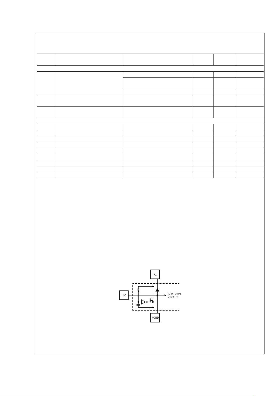
Note 7: The analog inputs are protected as shown below. Input voltage magnitudes up to V
A
+ 300 mV or to 300 mV below GND will not damage this device.
However, errors in the A/D conversion can occur if the input goes above DR V
D
or below GND by more than 100 mV. For example, if VAis 2.7VDCthe full-scale input
voltage must be ≤2.6V
DC
to ensure accurate conversions.
20006207
Note 8: To guarantee accuracy, it is required that VAand DR VDbe well bypassed. Each supply pin must be decoupled with separate bypass capacitors.
Note 9: Typical figures are at T
J
= 25˚C, and represent most likely parametric norms. Test limits are guaranteed to National’s AOQL (Average Outgoing Quality
Level).
ADC08060
www.national.com 6
Page 7

Typical Performance Characteristics V
A
=DRVD= 3V, f
CLK
= 60 MHz, fIN= 10 MHz, unless other-
wise stated
INL INL vs Temperature
20006208
20006214
INL vs Supply Voltage INL vs Sample Rate
20006215
20006210
DNL DNL vs Temperature
20006209
20006217
ADC08060
www.national.com7
Page 8

Typical Performance Characteristics V
A
=DRVD= 3V, f
CLK
= 60 MHz, fIN= 10 MHz, unless
otherwise stated (Continued)
DNL vs Supply Voltage DNL vs Sample Rate
20006218
20006211
SNR vs Temperature SNR vs Supply Voltage
20006220 20006221
SNR vs Sample Rate SNR vs Input Frequency
20006212 20006223
ADC08060
www.national.com 8
Page 9

Typical Performance Characteristics V
A
=DRVD= 3V, f
CLK
= 60 MHz, fIN= 10 MHz, unless
otherwise stated (Continued)
SNR vs Clock Duty Cycle Distortion vs Temperature
20006224 20006225
Distortion vs Supply Voltage Distortion vs Sample Rate
20006226 20006213
Distortion vs Input Frequency Distortion vs Clock Duty Cycle
20006228 20006229
ADC08060
www.national.com9
Page 10

Typical Performance Characteristics V
A
=DRVD= 3V, f
CLK
= 60 MHz, fIN= 10 MHz, unless
otherwise stated (Continued)
SINAD/ENOB vs Temperature SINAD/ENOB vs Supply Voltage
20006230
20006238
SINAD/ENOB vs Sample Rate SINAD/ENOB vs Input Frequency
20006216 20006239
SINAD/ENOB vs Clock Duty Cycle Power Consumption vs Sample Rate
20006240 20006219
ADC08060
www.national.com 10
Page 11

Typical Performance Characteristics V
A
=DRVD= 3V, f
CLK
= 60 MHz, fIN= 10 MHz, unless
otherwise stated (Continued)
Spectral Response
@
fIN= 10.1 MHz Spectral Response@fIN= 25 MHz
20006244 20006245
Intermodulation Distortion (IMD)
20006242
ADC08060
www.national.com11
Page 12

Specification Definitions
APERTURE (SAMPLING) DELAY is that time required after
the fall of the clock input for the sampling switch to open. The
Sample/Hold circuit effectively stops capturing the input signal and goes into the “hold” mode t
AD
after the clock goes
low.
APERTURE JITTER is the variation in aperture delay from
sample to sample. Aperture jitter shows up as noise at the
output.
CLOCK DUTY CYCLE is the ratio of the time that the clock
wavesform is at a logic high to the total time of one clock
period.
DIFFERENTIAL NON-LINEARITY (DNL) is the measure of
the maximum deviation from the ideal step size of 1 LSB.
Measured at 60 MSPS with a ramp input.
EFFECTIVE NUMBER OF BITS (ENOB, or EFFECTIVE
BITS) is another method of specifying Signal-to-Noise and
Distortion Ratio, or SINAD. ENOB is defined as (SINAD –
1.76) / 6.02 and says that the converter is equivalent to a
perfect ADC of this (ENOB) number of bits.
FULL-POWER BANDWIDTH is the frequency at which the
reconstructed output fundamental drops 3 dB below its low
frequency value for a full scale input.
FULL-SCALE ERROR is a measure of how far the last code
transition is from the ideal 1
1
⁄2LSB below VRTand is defined
as:
V
max
+ 1.5 LSB – V
RT
where V
max
is the voltage at which the transition to the
maximum (full scale) code occurs.
INTEGRAL NON-LINEARITY (INL) is a measure of the
deviation of each individual code from a line drawn from zero
scale (
1
⁄2LSB below the first code transition) through positive
full scale (
1
⁄2LSB above the last code transition). The deviation of any given code from this straight line is measured
from the center of that code value. The end point test method
is used. Measured at 60 MSPS with a ramp input.
INTERMODULATION DISTORTION (IMD) is the creation of
additional spectral components as a result of the interaction
between two sinusoidal frequencies that are applied to the
ADC input at the same time. IMD is the ratio of the power in
the second and third order intermodulation products to the
total power in the original frequencies.
MISSING CODES are those output codes that are skipped
and will never appear at the ADC outputs. These codes
cannot be reached with any input value.
POWER SUPPLY REJECTION RATIO (PSRR) is a measure of how well the ADC rejects a change in the power
supply voltage. For the ADC08060, PSRR1 is the ratio of the
change in dc power supply voltage to the resulting change in
Full-Scale Error, expressed in dB. PSRR2 is a measure of
how well an a.c. signal riding upon the power supply is
rejected and is here defined as:
where SNR0 is the SNR measured with no noise or signal on
the supply lines and SNR1 is the SNR measured with a 200
kHz, 200 mV
P-P
signal riding upon the supply lines.
OUTPUT DELAY is the time delay after the rising edge of
the input clock before the data changes at the output pins.
OUTPUT HOLD TIME is the length of time that the output
data is valid after the rise of the input clock.
PIPELINE DELAY (LATENCY) is the number of clock cycles
between initiation of conversion and when that data is presented to the output driver stage. New data is available at
every clock cycle, but the data lags the conversion by the
Pipeline Delay plus the Output Delay.
SIGNAL TO NOISE RATIO (SNR) is the ratio, expressed in
dB, of the rms value of the input signal frequency at the
output to the rms value of the sum of all other spectral
components below one-half the sampling frequency, not including harmonics or dc.
SIGNAL TO NOISE PLUS DISTORTION (S/(N+D) or
SINAD) is the ratio, expressed in dB, of the rms value of the
input signal frequency at the output to the rms value of all of
the other spectral components below half the clock frequency, including harmonics but excluding dc.
SPURIOUS FREE DYNAMIC RANGE (SFDR) is the difference, expressed in dB, between the rms values of the input
signal frequency at the output and the peak spurious signal,
where a spurious signal is any signal present in the output
spectrum that is not present at the input.
TOTAL HARMONIC DISTORTION (THD) is the ratio, expressed in dB, of the total of the first nine harmonic levels at
the output to the level of the fundatmental at the output. THD
is calculated as
where f1is the RMS power of the fundamental (input) frequency and f
2
through f10is the power in the first 9 harmon-
ics in the output spectrum.
ZERO SCALE OFFSET ERROR is the error in the input
voltage required to cause the first code transition. It is defined as
V
OFF=VZT−VRB
where VZTis the first code transition input voltage.
ADC08060
www.national.com 12
Page 13

Timing Diagram
Functional Description
The ADC08060 uses a new, unique architecture that
achieves over 7.4 effective bits at input frequencies up to
30 MHz.
The analog input signal that is within the voltage range set by
V
RT
and VRBis digitized to eight bits. Output format is
straight binary. Input voltages below V
RB
will cause the
output word to consist of all zeroes. Input voltages above
V
RB
will cause the output word to consist of all ones.
Incorporating a switched capacitor bandgap, the ADC08060
exhibits a power consumption that is proportional to frequency, limiting power consumption to what is needed at the
clock rate that is used. This and its excellent performance
over a wide range of clock frequencies makes it an ideal
choice as a single ADC for many 8-bit needs.
Data is acquired at the falling edge of the clock and the
digital equivalent of that data is available at the digital outputs 2.5 clock cycles plus t
OD
later. The ADC08060 will
convert as long as the clock signal is present. The device is
in the active state when the Power Down pin (PD) is low.
When the PD pin is high, the device is in the power down
mode, where the output pins hold the last conversion before
the PD pin went high and the device consumes just 1 mW.
Applications Information
1.0 REFERENCE INPUTS
The reference inputs V
RT
and VRBare the top and bottom of
the reference ladder, respectively. Input signals between
these two voltages will be digitized to 8 bits. External voltages applied to the reference input pins should be within the
range specified in the Operating Ratings table (1.0V to (V
A
+
0.1V) for V
RT
and 0V to (VRT− 1.0V) for VRB). Any device
used to drive the reference pins should be able to source
sufficient current into the V
RT
pin and sink sufficient current
from the V
RB
pin.
20006231
FIGURE 1. ADC08060 Timing Diagram
ADC08060
www.national.com13
Page 14

Applications Information (Continued)
The reference bias circuit of Figure 2 is very simple and the
performance is adequate for many applications. However,
circuit tolerances will lead to a wide reference voltage range.
Superior performance can generally be achieved by driving
the reference pins with a low impedance source.
The circuit of Figure 3 will allow a more accurate setting of
the reference voltages. The lower amplifier must have bipolar supplies as its output voltage must go negative to force
V
RB
to any voltage below the VBEof the PNP transistor. Of
course, the divider resistors at the amplifier input could be
changed to suit your reference voltage needs, or the divider
can be replaced with potentiometers for precise settings.
The bottom of the ladder (V
RB
) may simply be returned to
ground if the minimum input signal excursion is 0V. Be sure
that the driving sources can source sufficient current into the
V
RT
pin and sink enough current from the VRBpin to keep
these pins stable.
The LMC662 amplifier shown was chosen for its low offset
voltage and low cost.
20006232
FIGURE 2. Simple, low component count reference biasing. Because of the ladder and external resistor tolerances,
the reference voltage can vary too much for some applications.
ADC08060
www.national.com 14
Page 15

Applications Information (Continued)
V
RT
should always be at least 1.0V more positive than V
RB
to minimize noise.
V
RM
(pin 9) is the center of the reference ladder and should
be bypassed to a clean, quiet point in the analog ground
plane with a 0.1 µF capacitor. DO NOT allow this pin to float.
2.0 THE ANALOG INPUT
The analog input of the ADC08060 is a switch followed by an
integrator. The input capacitance changes with the clock
level, appearing as 3 pF when the clock is low, and 4 pF
when the clock is high. Since a dynamic capacitance is more
difficult to drive than is a fixed capacitance, choose an
amplifier that can drive this type of load. The LMH6702 has
been found to be a good amplifier to drive the ADC08060.
Figure 4 shows an example of an input circuit using the
LMH6702. Any input amplifier should incorporate some gain
as operational amplifiers exhibit better phase margin and
transient response with gains above 2 or 3 than with unity
gain. If an overall gain of less than 3 is required, attenuate
the input and operate the amplifier at a higher gain, as
shown in Figure 4.
20006233
FIGURE 3. Driving the reference to force desired values requires driving with a low impedance source.
ADC08060
www.national.com15
Page 16

Applications Information (Continued)
The RC at the amplifier output filters the clock rate energy
that comes out of the analog input due to the input sampling
circuit. The optimum time constant for this circuit depends
not only upon the amplifier and ADC, but also on the circuit
layout and board material. A resistor value should be chosen
between 18Ω and 47Ω and the capacitor value chose according to the formula
This will provide optimum SNR performance. Best THD performance is realized when the capacitor and resistor values
are both zero. To optimize SINAD, reduce the capacitor
value until SINAD performance is optimized. That is, until
SNR = −THD. This value will usually be in the range of 40%
to 65% of the value calculated with the above formula. An
accurate calculation is not possible because of the board
material and layout dependance.
The above is indended for oversampling or Nyquist applications. There should be no resistor or capacitor between the
ADC input and any amplifier for undersampling applications.
The circuit of Figure 4 has both gain and offset adjustments.
If you eliminate these adjustments normal circuit tolerances
may cause signal clipping unless care is exercised in the
worst case analysis of component tolerances and the input
signal excursion is appropriately limited to account for the
worst case conditions. Of course, this means that the designer will not be able to count on getting a full scale output
with maximum signal input.
3.0 POWER SUPPLY CONSIDERATIONS
A/D converters draw sufficient transient current to corrupt
their own power supplies if not adequately bypassed. A
10 µF tantalum or aluminum electrolytic capacitor should be
placed within an inch (2.5 cm) of the A/D power pins, with a
0.1 µF ceramic chip capacitor placed within one centimeter
of the converter’s power supply pins. Leadless chip capacitors are preferred because they have low lead inductance.
While a single voltage source is recommended for the V
A
and DR VDsupplies of the ADC08060, these supply pins
should be well isolated from each other to prevent any digital
noise from being coupled into the analog portions of the
ADC. A choke or 27Ω resistor is recommended between
these supply lines with adequate bypass capacitors close to
the supply pins.
As is the case with all high speed converters, the ADC08060
should be assumed to have little power supply rejection.
None of the supplies for the converter should be the supply
that is used for other digital circuitry in any system with a lot
of digital power being consumed. The ADC supplies should
be the same supply used for other analog circuitry.
No pin should ever have a voltage on it that is in excess of
the supply voltage or below ground by more than 300 mV,
not even on a transient basis. This can be a problem upon
application of power and power shut-down. Be sure that the
supplies to circuits driving any of the input pins, analog or
digital, do not come up any faster than does the voltage at
the ADC08060 power pins.
20006234
FIGURE 4. The input amplifier should incorporate some gain for best performance (see text).
ADC08060
www.national.com 16
Page 17

Applications Information (Continued)
4.0 THE DIGITAL INPUT PINS
The ADC08060 has two digital input pins: The PD pin and
the Clock pin.
4.1 The PD Pin
The Power Down (PD) pin, when high, puts the ADC08060
into a low power mode where power consumption is reduced
to 1 mW. Output data is valid and accurate about 1 millisecond after the PD pin is brought low.
The digital output pins retain the last conversion output code
when either the clock is stopped or the PD pin is high.
4.2 The ADC08060 Clock
Although the ADC08060 is tested and its performance is
guaranteed with a 60 MHz clock, it typically will function well
with clock frequencies from 20 MHz to 70 MHz.
Halting the clock will provide nearly as much power saving
as raising the PD pin high. Typical power consumption with a
stopped clock is 3 mW, compared to 1 mW when PD is high.
The digital outputs will remain in the same state as they were
before the clock was halted.
Once the clock is restored (or the PD pin is brought low),
there is a time of 2.5 clock cycles plus t
OD
before the output
data is valid. However, because of the linear relationship
between total power consumption and clock frequency, the
part requires several microseconds after the clock is restarted or substantially changed in frequency before the part
returns to its specified accuracy.
The low and high times of the clock signal can affect the
performance of any A/D Converter. Because achieving a
precise duty cycle is difficult, the ADC08060 is designed to
maintain performance over a range of duty cycles. While it is
specified and performance is guaranteed with a 50% clock
duty cycle and 60 Msps, ADC08060 performance is typically
maintained with clock high and low times of 6.7 ns, corresponding to a clock duty cycle range of 40% to 50% with a
60 MHz clock.
The CLOCK line should be series terminated at the clock
source in the characteristic impedance of that line. If the
clock line is longer than
where tris the clock rise time and tPDis the propagation rate
of the signal along the trace, the CLOCK pin should be a.c.
terminated with a series RC to ground such that the resistor
value is equal to the characteristic impedance of the clock
line and the capacitor value is
where tPDis the signal propagation rate down the clock line,
"L" is the line length and Z
o
is the characteristic impedance
of the clock line. This termination should be located as close
as possible to, but within one centimeter of, the ADC08060
clock pin. Typical t
PD
is about 150 ps/inch on FR-4 board
material. For FR-4 board material, the value of C becomes
where L is the length of the clock line in inches.
5.0 LAYOUT AND GROUNDING
Proper grounding and proper routing of all signals are essential to ensure accurate conversion. A combined analog
and digital ground plane should be used.
Since digital switching transients are composed largely of
high frequency components, total ground plane copper
weight will have little effect upon the logic-generated noise
because of the skin effect. Total surface area is more important than is total ground plane volume. Capacitive coupling
between the typically noisy digital circuitry and the sensitive
analog circuitry can lead to poor performance that may seem
impossible to isolate and remedy. The solution is to keep the
analog circuitry well separated from the digital circuitry.
High power digital components should not be located on or
near a straight line between the ADC (or any linear component) and the power supply area as the resulting common
return current path could cause fluctuation in the analog
“ground” return of the ADC.
Generally, analog and digital lines should cross each other at
90˚ to avoid getting digital noise into the analog path. In high
frequency systems, however, avoid crossing analog and
digital lines altogether. Clock lines should be isolated from
ALL other lines, analog AND digital. Even the generally
accepted 90˚ crossing should be avoided as even a little
coupling can cause problems at high frequencies. Best performance at high frequencies is obtained with a straight
signal path.
The analog input should be isolated from noisy signal traces
to avoid coupling of spurious signals into the input. Any
external component (e.g., a filter capacitor) connected between the converter’s input and ground should be connected
to a very clean point in the analog ground plane.
20006236
FIGURE 5. Layout Example
ADC08060
www.national.com17
Page 18

Applications Information (Continued)
Figure 5 gives an example of a suitable layout. All analog
circuitry (input amplifiers, filters, reference components, etc.)
should be placed together away from any digital components.
6.0 DYNAMIC PERFORMANCE
The ADC08060 is ac tested and its dynamic performance is
guaranteed. To meet the published specifications, the clock
source driving the CLK input must exhibit less than 10 ps
(rms) of jitter. For best ac performance, isolating the ADC
clock from any digital circuitry should be done with adequate
buffers, as with a clock tree. See Figure 6.
It is good practice to keep the ADC clock line as short as
possible and to keep it well away from any other signals.
Other signals can introduce jitter into the clock signal. The
clock signal can also introduce noise into the analog path.
7.0 COMMON APPLICATION PITFALLS
Driving the inputs (analog or digital) beyond the power
supply rails. For proper operation, all inputs should not go
more than 300 mV below the ground pins or 300 mV above
the supply pins. Exceeding these limits on even a transient
basis may cause faulty or erratic operation. It is not uncommon for high speed digital circuits (e.g., 74F and 74AC
devices) to exhibit undershoot that goes more than a volt
below ground. A 51Ω resistor in series with the offending
digital input will usually eliminate the problem.
Care should be taken not to overdrive the inputs of the
ADC08060. Such practice may lead to conversion inaccuracies and even to device damage.
Attempting to drive a high capacitance digital data bus.
The more capacitance the output drivers must charge for
each conversion, the more instantaneous digital current is
required from DR V
D
and DR GND. These large charging
current spikes can couple into the analog section, degrading
dynamic performance. Buffering the digital data outputs (with
a 74F541, for example) may be necessary if the data bus
capacitance exceeds 10 pF. Dynamic performance can also
be improved by adding 47Ω to 56Ω series resistors at each
digital output, reducing the energy coupled back into the
converter input pins.
Using an inadequate amplifier to drive the analog input.
As explained in Section 2.0, the capacitance seen at the
input alternates between 3 pF and 4 pF with the clock. This
dynamic capacitance is more difficult to drive than is a fixed
capacitance, and should be considered when choosing a
driving device. The LMH6702 has been found to be a good
device for driving the ADC08060.
Driving the V
RT
pin or the VRBpin with devices that can
not source or sink the current required by the ladder.
As mentioned in Section 1.0, care should be taken to see
that any driving devices can source sufficient current into the
V
RT
pin and sink sufficient current from the VRBpin. If these
pins are not driven with devices than can handle the required
current, these reference pins will not be stable, resulting in a
reduction of dynamic performance.
Using a clock source with excessive jitter, using an
excessively long clock signal trace, or having other
signals coupled to the clock signal trace. This will cause
the sampling interval to vary, causing excessive output noise
and a reduction in SNR performance. The use of simple
gates with RC timing is generally inadequate as a clock
source.
20006237
FIGURE 6. Isolating the ADC Clock from Digital
Circuitry
ADC08060
www.national.com 18
Page 19

Physical Dimensions inches (millimeters) unless otherwise noted
NOTES: UNLESS OTHERWISE SPECIFIED
REFERENCE JECED REGISTRATION mo-153, VARIATION AD, DATED 7/93.
24-Lead Package TC
Order Number ADC08060CIMT
NS Package Number MTC24
LIFE SUPPORT POLICY
NATIONAL’S PRODUCTS ARE NOT AUTHORIZED FOR USE AS CRITICAL COMPONENTS IN LIFE SUPPORT
DEVICES OR SYSTEMS WITHOUT THE EXPRESS WRITTEN APPROVAL OF THE PRESIDENT AND GENERAL
COUNSEL OF NATIONAL SEMICONDUCTOR CORPORATION. As used herein:
1. Life support devices or systems are devices or
systems which, (a) are intended for surgical implant
into the body, or (b) support or sustain life, and
whose failure to perform when properly used in
accordance with instructions for use provided in the
labeling, can be reasonably expected to result in a
significant injury to the user.
2. A critical component is any component of a life
support device or system whose failure to perform
can be reasonably expected to cause the failure of
the life support device or system, or to affect its
safety or effectiveness.
National Semiconductor
Americas Customer
Support Center
Email: new.feedback@nsc.com
Tel: 1-800-272-9959
National Semiconductor
Europe Customer Support Center
Fax: +49 (0) 180-530 85 86
Email: europe.support@nsc.com
Deutsch Tel: +49 (0) 69 9508 6208
English Tel: +44 (0) 870 24 0 2171
Français Tel: +33 (0) 1 41 91 8790
National Semiconductor
Asia Pacific Customer
Support Center
Fax: 65-6250 4466
Email: ap.support@nsc.com
Tel: 65-6254 4466
National Semiconductor
Japan Customer Support Center
Fax: 81-3-5639-7507
Email: nsj.crc@jksmtp.nsc.com
Tel: 81-3-5639-7560
www.national.com
ADC08060 8-Bit, 60 MSPS, 1.3 mW/MSPS A/D Converter
National does not assume any responsibility for use of any circuitry described, no circuit patent licenses are implied and National reserves the right at any time without notice to change said circuitry and specifications.
 Loading...