

Datasheet ADC08038CMJ, ADC08038BIWM, ADC08038BIN, ADC08034CIN, ADC08034BIWM Datasheet (NSC)
...Page 1
ADC08031/ADC08032/ADC08034/ADC08038
8-Bit High-Speed Serial I/O A/D Converters with
Multiplexer Options, Voltage Reference, and Track/Hold
Function
General Description
The ADC08031/ADC08032/ADC08034/ADC08038 are 8-bit
successive approximationA/D converters with serial I/O and
configurable input multiplexers with up to 8 channels. The
serial I/O is configured to comply with the NSC MICROWIRE
™
serial data exchangestandard for easy interface tothe
COPS
™
family of controllers, and can easily interface with
standard shift registers or microprocessors.
TheADC08034 and ADC08038 provide a 2.6V band-gap de-
rived reference. For devices offeringguaranteed voltage reference performance over temperature see ADC08131,
ADC08134 and ADC08138.
Atrack/hold function allowsthe analog voltage at thepositive
input to vary during the actual A/D conversion.
The analog inputs can be configured to operate in various
combinations of single-ended, differential, or
pseudo-differential modes. In addition, input voltage spans
as small as 1V can be accommodated.
Applications
n Digitizing automotive sensors
n Process control monitoring
n Remote sensing in noisy environments
n Instrumentation
n Test systems
n Embedded diagnostics
Features
n Serial digital data link requires few I/O pins
n Analog input track/hold function
n 2-, 4-, or 8-channel input multiplexer options with
address logic
n 0V to 5V analog input range with single 5V power
supply
n No zero or full scale adjustment required
n TTL/CMOS input/output compatible
n On chip 2.6V band-gap reference
n 0.3" standard width 8-, 14-, or 20-pin DIP package
n 14-, 20-pin small-outline packages
Key Specifications
n Resolution: 8 bits
n Conversion time (f
C
= 1 MHz): 8µs (max)
n Power dissipation: 20mW (max)
n Single supply: 5V
DC
(±5%)
n Total unadjusted error:
±
1
⁄2LSB and±1LSB
n No missing codes over temperature
Ordering Information
Industrial (−40˚C ≤ TA≤ +85˚C) Package
ADC08031CIN* N08E
ADC08038CIN* N20A
ADC08031CIWM,
ADC08032CIWM, M14B
ADC08034CIWM
ADC08038CIWM M20B
*
Not recomended for new designs.
COPS™microcontrollers and MICROWIRE™are trademarks of National Semiconductor Corporation.
June 2000
ADC08031/ADC08032/ADC08034/ADC08038 8-Bit High-Speed Serial I/O A/D Converters with
Multiplexer Options, Voltage Reference, and Track/Hold Function
© 2000 National Semiconductor Corporation DS010555 www.national.com
Page 2
Connection Diagrams
ADC08038
DS010555-2
ADC08034
DS010555-3
ADC08031
Dual-In-Line Package
DS010555-5
ADC08032
Small Outline Package
DS010555-30
ADC08031
Small Outline Package
DS010555-31
ADC08031/ADC08032/ADC08034/ADC08038
www.national.com 2
Page 3
Absolute Maximum Ratings (Notes 1, 3)
If Military/Aerospace specified devices are required,
please contact the National Semiconductor Sales Office/
Distributors for availability and specifications.
Supply Voltage (V
CC
) 6.5V
Voltage at Inputs and Outputs −0.3V to V
CC
+ 0.3V
Input Current at Any Pin (Note 4)
±
5mA
Package Input Current (Note 4)
±
20 mA
Power Dissipation at T
A
= 25˚C
(Note 5) 800 mW
ESD Susceptibility (Note 6) 1500V
Soldering Information
N Package (10 sec.)
SO Package:
Vapor Phase (60 sec.)
Infrared (15 sec.) (Note 7)
235˚C
215˚C
220˚C
Storage Temperature −65˚C to +150˚C
Operating Ratings (Notes 2, 3)
Temperature Range T
MIN
≤ TA≤ T
MAX
ADC08031BIN, ADC08031CIN, −40˚C ≤ TA≤ +85˚C
ADC08032BIN, ADC08032CIN,
ADC08034BIN, ADC08034CIN,
ADC08038BIN, ADC08038CIN,
ADC08031BIWM, ADC08032BIWM,
ADC08034BIWM, ADC08038BIWM
ADC08031CIWM, ADC08032CIWM,
ADC08034CIWM, ADC08038CIWM
Supply Voltage (V
CC
) 4.5 VDCto 6.3 V
DC
Electrical Characteristics
The following specifications apply for VCC=V
REF
=+5VDC, and f
CLK
= 1 MHz unless otherwise specified. Boldface limits
apply for TA=TJ=T
MIN
to T
MAX
; all other limits TA=TJ= 25˚C.
Symbol Parameter Conditions Typical Limits Units
(Note 8) (Note 9) (Limits)
CONVERTER AND MULTIPLEXER CHARACTERISTICS
Total Unadjusted Error (Note 10)
BIN, BIWM
±
1
⁄
2
LSB (max)
CIN, CIWM
±
1 LSB (max)
Differential 8 Bits (min)
Linearity
R
REF
Reference Input Resistance (Note 11) 3.5 kΩ
1.3 kΩ (min)
6.0 kΩ (max)
V
IN
Analog Input Voltage (Note 12) (VCC+ 0.05) V (max)
(GND − 0.05) V (min)
DC Common-Mode Error
±
1
⁄
4
LSB (max)
Power Supply Sensitivity V
CC
=5V±5%,
±
1
⁄
4
LSB (max)
V
REF
= 4.75V
On Channel Leakage On Channel = 5V, 0.2 µA (max)
Current (Note 13) Off Channel = 0V 1
On Channel = 0V, −0.2 µA (max)
Off Channel = 5V −1
Off Channel Leakage On Channel = 5V, −0.2 µA (max)
Current (Note 13) Off Channel = 0V −1
On Channel = 0V, 0.2 µA (max)
Off Channel = 5V 1
DIGITAL AND DC CHARACTERISTICS
V
IN(1)
Logical “1” Input Voltage VCC= 5.25V 2.0 V (min)
V
IN(0)
Logical “0” Input Voltage VCC= 4.75V 0.8 V (max)
I
IN(1)
Logical “1” Input Current VIN= 5.0V 1 µA (max)
I
IN(0)
Logical “0” Input Current VIN=0V −1 µA (max)
V
OUT(1)
Logical “1” Output Voltage VCC= 4.75V:
I
OUT
= −360 µA 2.4 V (min)
I
OUT
= −10 µA 4.5 V (min)
V
OUT(0)
Logical “0” Output Voltage VCC= 4.75V 0.4 V (max)
I
OUT
= 1.6 mA
ADC08031/ADC08032/ADC08034/ADC08038
www.national.com3
Page 4
Electrical Characteristics (Continued)
The following specifications apply for VCC=V
REF
=+5VDC, and f
CLK
= 1 MHz unless otherwise specified. Boldface limits
apply for TA=TJ=T
MIN
to T
MAX
; all other limits TA=TJ= 25˚C.
Symbol Parameter Conditions Typical Limits Units
(Note 8) (Note 9) (Limits)
DIGITAL AND DC CHARACTERISTICS
I
OUT
TRI-STATE®Output Current V
OUT
=0V −3.0 µA (max)
V
OUT
=5V 3.0 µA (max)
I
SOURCE
Output Source Current V
OUT
=0V −6.5 mA (min)
I
SINK
Output Sink Current V
OUT=VCC
8.0 mA (min)
I
CC
Supply Current
ADC08031, ADC08034, CS = HIGH
3.0 mA (max)
and ADC08038
ADC08032 (Note 16) 7.0 mA (max)
REFERENCE CHARACTERISTICS
V
REF
OUT Nominal Reference Output V
REF
OUT Option
Available Only on 2.6 V
ADC08034 and
ADC08038
Electrical Characteristics
The following specifications apply for VCC=V
REF
=+5VDC, and tr=tf= 20 ns unless otherwise specified. Boldface limits
apply for TA=TJ=T
MIN
to T
MAX
; all other limits TA=TJ= 25˚C.
Symbol Parameter Conditions Typical Limits Units
(Note 8) (Note 9) (Limits)
f
CLK
Clock Frequency 10 kHz (min)
1 MHz (max)
Clock Duty Cycle 40 % (min)
(Note 14) 60 % (max)
T
C
Conversion Time (Not Including f
CLK
= 1 MHz 8 1/f
CLK
(max)
MUX Addressing Time) 8 µs (max)
t
CA
Acquisition Time
1
⁄
2
1/f
CLK
(max)
t
SELECT
CLK High while CS is High 50 ns
t
SET-UP
CS Falling Edge or Data Input 25 ns (min)
Valid to CLK Rising Edge
t
HOLD
Data Input Valid after CLK 20 ns (min)
Rising Edge
t
pd1,tpd0
CLK Falling Edge to Output CL= 100 pF:
Data Valid (Note 15) Data MSB First 250 ns (max)
Data LSB First 200 ns (max)
t
1H,t0H
TRI-STATE Delay from Rising Edge CL= 10 pF, RL=10kΩ 50 ns
of CS to Data Output and SARS Hi-Z
(see TRI-STATE Test Circuits)
C
L
= 100 pF, RL=2kΩ 180 ns (max)
C
IN
Capacitance of Logic Inputs 5 pF
C
OUT
Capacitance of Logic Outputs 5 pF
Note 1: Absolute Maximum Ratings indicate limits beyond which damage to the device may occur.
Note 2: Operating Ratings indicate conditions for which the device is functional. These ratings do not guarantee specific performance limits. For guaranteed speci-
fications and test conditions, see the Electrical Characteristics. The guaranteed specifications apply only for the test conditions listed. Some performance characteristics may degrade when the device is not operated under the listed test conditions.
Note 3: All voltages are measured with respect to AGND = DGND = 0 V
DC
, unless otherwise specified.
Note 4: When the input voltage V
IN
at any pin exceeds the power supplies (V
IN
<
(AGND or DGND) or V
IN
>
VCC) the current at that pin should be limited to 5 mA.
The 20 mA maximum package input current rating limits the number of pins that can safely exceed the power supplies with an input current of 5 mA to four pins.
Note 5: The maximum power dissipation must be derated at elevated temperatures and is dictated by T
JMAX
, θJAand the ambient temperature, TA. The maximum
allowable power dissipation at any temperature is P
D
=(T
JMAX−TA
)/θJAor the number given in the Absolute Maximum Ratings, whichever is lower. For these de-
ADC08031/ADC08032/ADC08034/ADC08038
www.national.com 4
Page 5
Electrical Characteristics (Continued)
vices, T
JMAX
= 125˚C. The typical thermal resistances (θJA) of these parts when board mounted follow: ADC08031 and ADC08032 with BIN and CIN suffixes
120˚C/W,ADC08038withCINsuffix80˚C/W.ADC08031 withCIWMsuffix140˚C/W,ADC08032 140˚C/W, ADC08034 140˚C/W,ADC08038with CIWM suffix 91˚C/W.
Note 6: Human body model, 100 pF capacitor discharged through a 1.5 kΩ resistor.
Note 7: See AN450 “Surface MountingMethods and Their Effect on Product Reliability” or Linear DataBook section “Surface Mount” for other methods of soldering
surface mount devices.
Note 8: Typicals are at T
J
= 25˚C and represent the most likely parametric norm.
Note 9: Guaranteed to National’s AOQL (Average Outgoing Quality Level).
Note 10: Total unadjusted error includes offset, full-scale, linearity, multiplexer.
Note 11: Cannot be tested for the ADC08032.
Note 12: For V
IN(−)
≥ V
IN(+)
the digital code will be 0000 0000. Twoon-chip diodes are tied to each analog input (see Block Diagram) which will forward-conduct for
analog input voltages one diode drop below ground or one diode drop greater than V
CC
supply.During testing at low VCClevels (e.g., 4.5V), high level analog inputs
(e.g., 5V) can cause an input diode to conduct, especially at elevated temperatures, which willcause errors for analog inputs near full-scale. The spec allows 50 mV
forward bias of either diode; this means that as long as the analog V
IN
does not exceed the supply voltage by more than 50 mV, the output code will be correct. Ex-
ceeding this range on an unselected channelwillcorrupt the reading of a selected channel. Achievement of an absolute 0V
DC
to5VDCinput voltage range will there-
fore require a minimum supply voltage of 4.950 V
DC
over temperature variations, initial tolerance and loading.
Note 13: Channel leakage currentis measured after a single-ended channelis selected and the clock isturned off. For off channel leakage currentthe following two
cases are considered: one, with the selected channel tied high (5 V
DC
) and the remaining seven off channels tied low (0 VDC), total current flow through the off channels is measured; two, withthe selected channel tied low and the off channels tied high, totalcurrent flow through the off channelsis again measured. The two cases
considered for determining on channel leakage current are the same except total current flow through the selected channel is measured.
Note 14: A 40% to 60% dutycycle range insures proper operation at all clock frequencies. In the case that an available clock hasa duty cycle outside of theselimits
the minimum time the clock is high or low must be at least 450 ns. The maximum time the clock can be high or low is 100 µs.
Note 15: Since data, MSB first, istheoutput of the comparator used in the successive approximationloop,an additional delay is built in (see Block Diagram) toallow
for comparator response time.
Note 16: For the ADC08032 V
REF
IN is internally tied to VCC, therefore, for the ADC08032 reference current is included in the supply current.
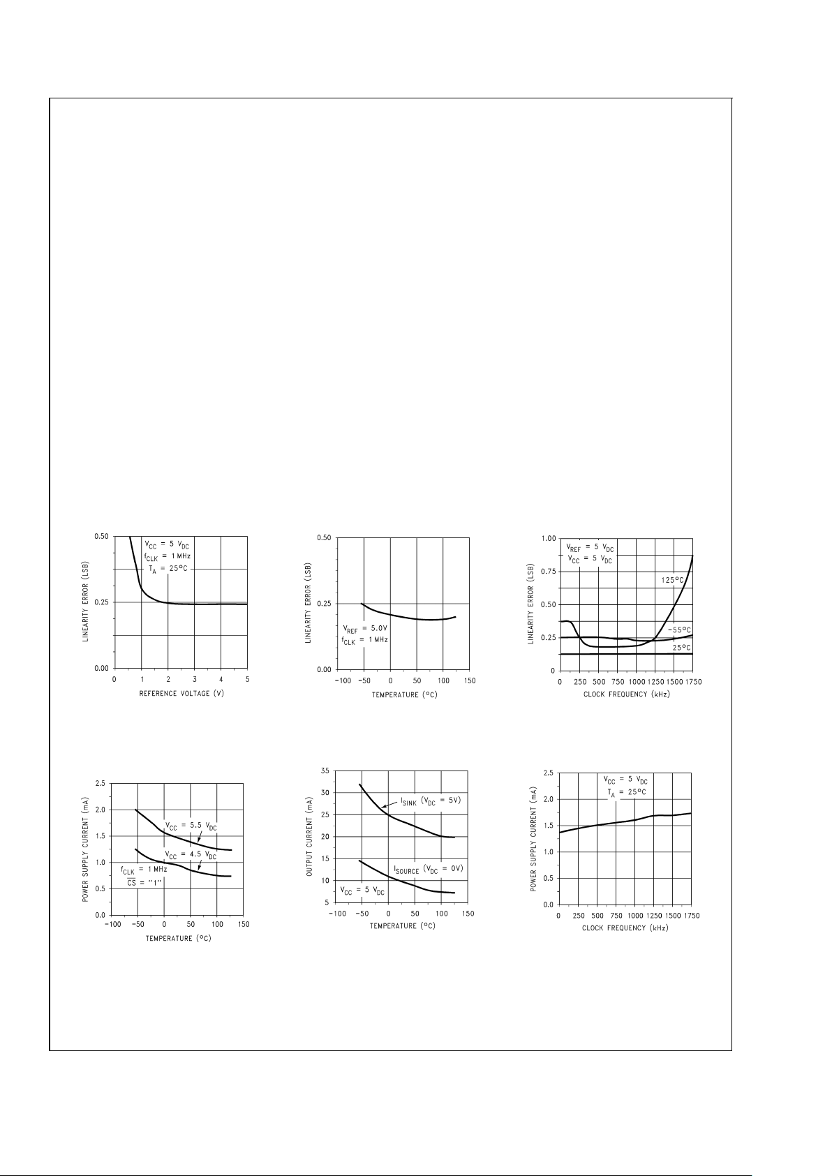
Typical Performance Characteristics
Linearity Error vs
Reference Voltage
DS010555-32
Linearity Error vs
Temperature
DS010555-33
Linearity Error vs
Clock Frequency
DS010555-34
Power Supply Current vs
Temperature (ADC08038,
ADC08034, ADC08031)
DS010555-35
Note: For ADC08032 add I
REF
Output Current vs
Temperature
DS010555-36
Power Supply Current
vs Clock Frequency
DS010555-37
ADC08031/ADC08032/ADC08034/ADC08038
www.national.com5
Page 6
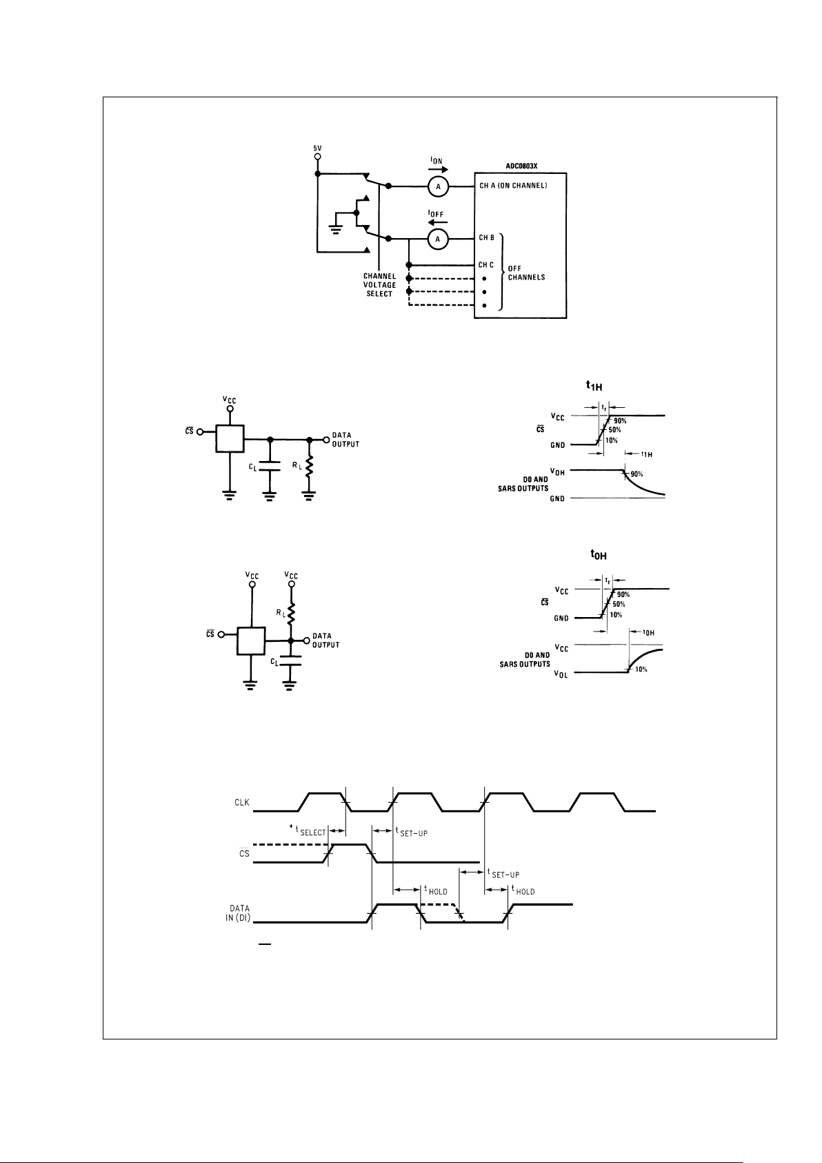
Leakage Current Test Circuit
TRI-STATE Test Circuits and Waveforms
Timing Diagrams
DS010555-7
t
1H
DS010555-38
DS010555-39
t
0H
DS010555-40
DS010555-41
Data Input Timing
DS010555-10
*To reset these devices, CLK and CS must be simultaneously high for a period of t
SELECT
or greater. Otherwise these devices are compatible with industry
standards ADC0831/2/4/8.
ADC08031/ADC08032/ADC08034/ADC08038
www.national.com 6
Page 7
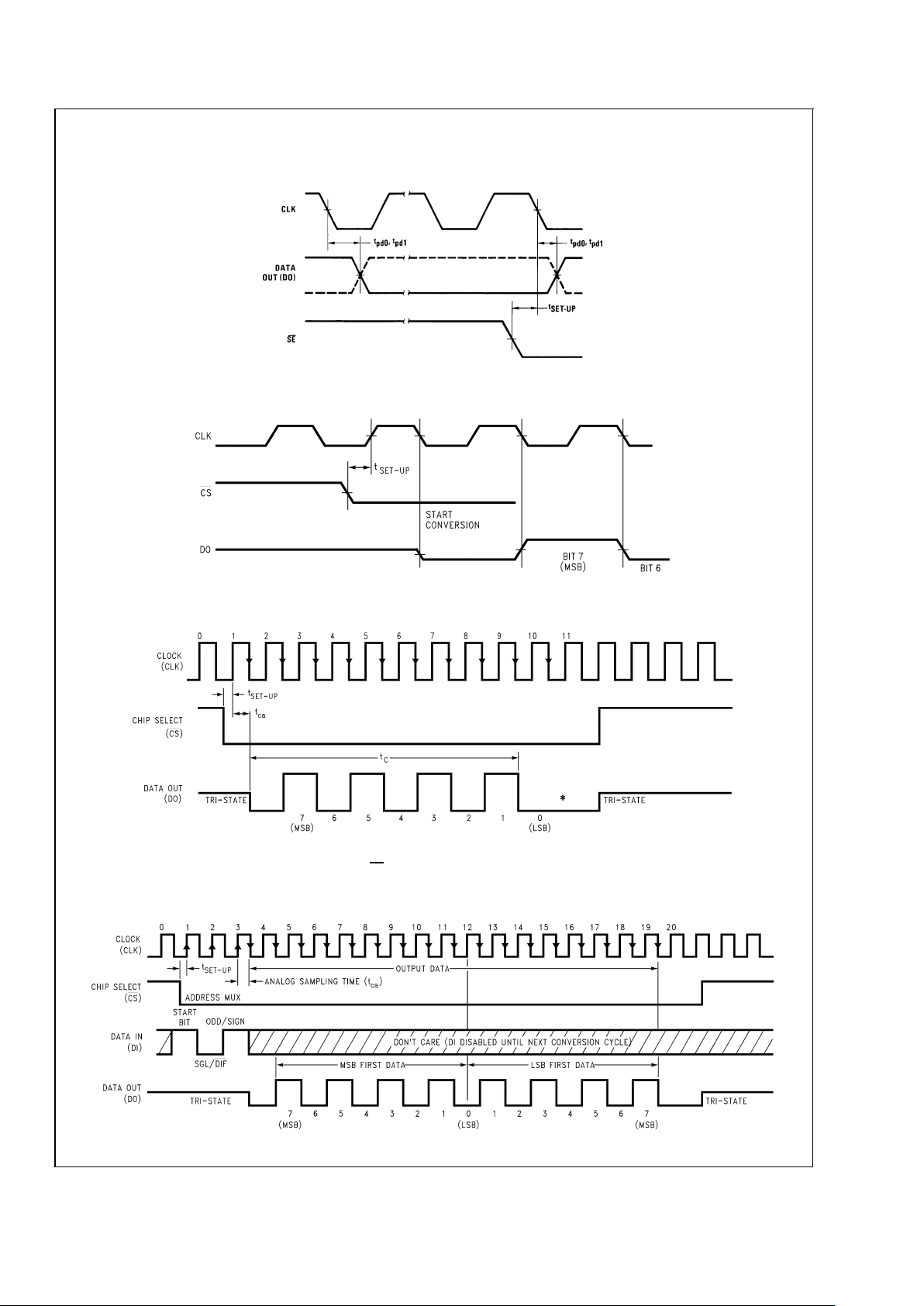
Timing Diagrams (Continued)
Data Output Timing
DS010555-11
ADC08031 Start Conversion Timing
DS010555-12
ADC08031 Timing
DS010555-13
*LSB first output not available on ADC08031.
LSB information is maintained for remainder of clock periods until CS goes high.
ADC08032 Timing
DS010555-14
ADC08031/ADC08032/ADC08034/ADC08038
www.national.com7
Page 8
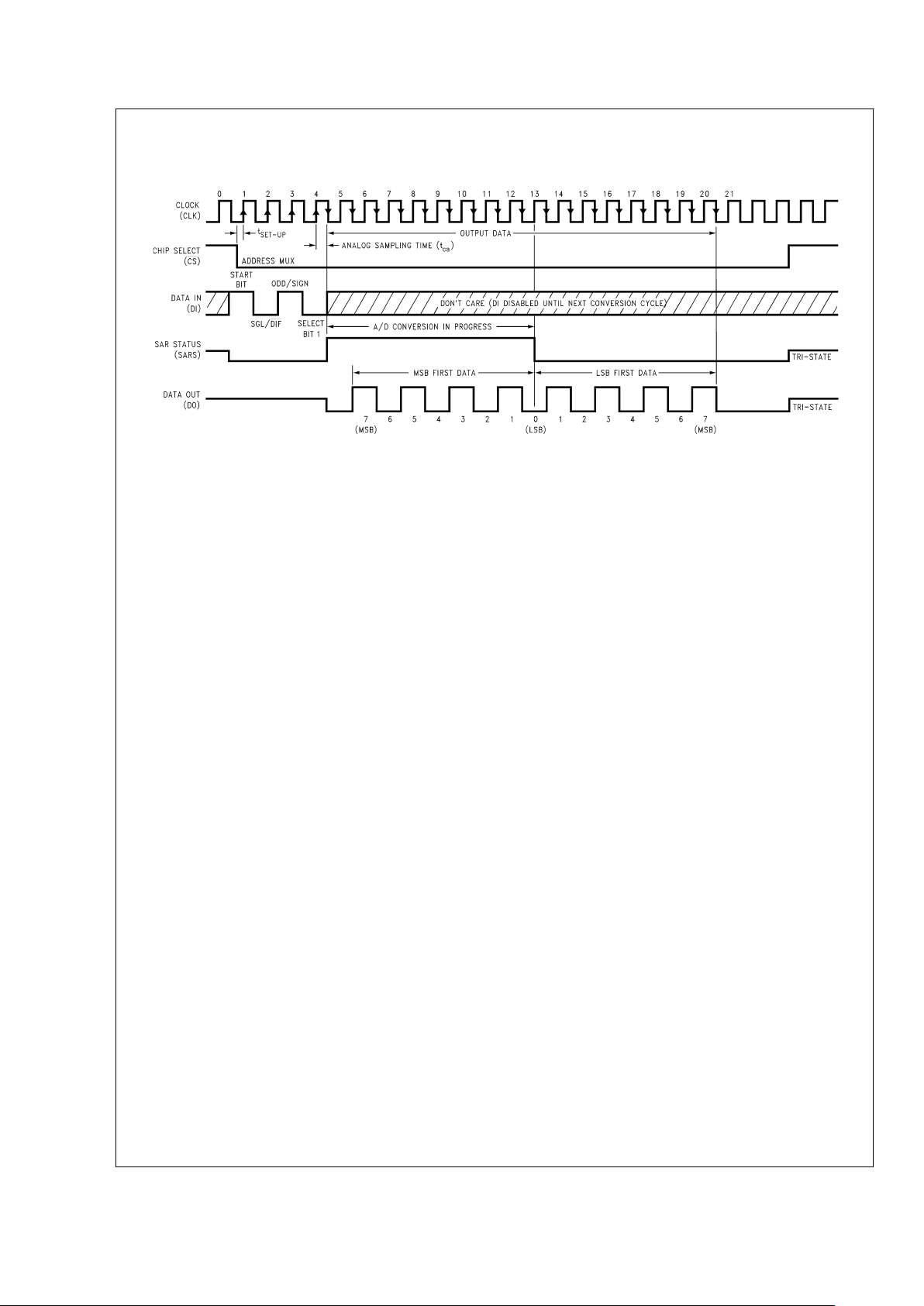
Timing Diagrams (Continued)
ADC08034 Timing
DS010555-15
ADC08031/ADC08032/ADC08034/ADC08038
www.national.com 8
Page 9

Timing Diagrams (Continued)
ADC08038 Timing
DS010555-16
*Make sure clock edge
#
18 clocks in the LSB before SE is taken low
ADC08031/ADC08032/ADC08034/ADC08038
www.national.com9
Page 10

ADC08038 Functional Block Diagram
Functional Description
1.0 MULTIPLEXER ADDRESSING
The design of these converters utilizes a comparator structure with built-in sample-and-hold which provides for a differential analog input to be converted by a successiveapproximation routine.
The actual voltage converted is always the difference between an assigned“+” input terminal and a “−” input terminal.
The polarity of each input terminal of the pair indicates which
line the converter expects to be the most positive. If the assigned “+” input voltage is less than the “−” input voltage the
converter responds with an all zeros output code.
A unique input multiplexing scheme has been utilized to provide multiple analog channels with software-configurable
single-ended, differential, or pseudo-differential (which will
convert the difference between the voltage at any analog input and a common terminal) operation. The analog signal
conditioning required in transducer-based data acquisition
systems is significantly simplified with this type of input flexibility. One converter package can now handle ground referenced inputs and true differential inputs as well as signals
with some arbitrary reference voltage.
A particular input configuration is assigned during the MUX
addressing sequence, prior to the start of a conversion. The
MUX address selects which of the analog inputs are to be
DS010555-17
*Some of these functions/pins are not available with other options.
For the ADC08034, the “SEL 1” Flip-Flop is bypassed, for the ADC08032, both “SEL 0” and “SEL 1” Flip-Flops are bypassed.
ADC08031/ADC08032/ADC08034/ADC08038
www.national.com 10
Page 11

Functional Description (Continued)
enabled and whetherthis input issingle-ended or differential.
Differential inputs are restricted to adjacent channel pairs.
For example, channel 0 and channel 1 may be selected as a
differential pair but channel 0 or 1 cannot act differentially
with any other channel. In addition to selecting differential
mode the polarity may also be selected. Channel 0 may be
selected as the positive input and channel 1 as the negative
input or viceversa. This programmabilityis best illustratedby
the MUX addressing codes shown in the following tables for
the various product options.
The MUX address is shifted into the converter via the DIline.
Because the ADC08031 contains only one differential input
channel with a fixed polarity assignment, it does not require
addressing.
The common input line (COM) on the ADC08038 can be
used as a pseudo-differential input. In this mode the voltage
on this pin is treated as the“−” input for any of the otherinput
channels. This voltage does not have to be analog ground; it
can be any reference potential which is common to all of the
inputs. This feature is most useful in single-supply applications where the analog circuity may be biased up to a potential other than ground and the output signals are all referred
to this potential.
TABLE 1. Multiplexer/Package Options
Part
Number
Number of Analog
Channels
Number of
Package
Pins
Single-Ended Differential
ADC08031 1 1 8
ADC08032 2 1 8
ADC08034 4 2 14
ADC08038 8 4 20
TABLE 2. MUX Addressing: ADC08038
Single-Ended MUX Mode
MUX Address Analog Single-Ended Channel
#
START SGL/ ODD/ SELECT 01234567COM
DIF
SIGN 1 0
11000+ −
11001 + −
11010 + −
11011 + −
11100 + −
11101 + −
11110 + −
11111 +−
TABLE 3. MUX Addressing: ADC08038
Differential MUX Mode
MUX Address Analog Differential Channel-Pair
#
START SGL/ ODD/ SELECT 0123
DIF
SIGN 1001234567
10000+−
10001 +−
10010 +−
10011 +−
10100−+
10101 −+
10110 −+
10111 −+
ADC08031/ADC08032/ADC08034/ADC08038
www.national.com11
Page 12

Functional Description (Continued)
TABLE 4. MUX Addressing: ADC08034
Single-Ended MUX Mode
MUX Address Channel
#
START SGL/ ODD/ SELECT 0123
DIF
SIGN 1
110 0+
110 1 +
111 0 +
111 1 +
COM is internally tied to AGND
MUX Addressing:
ADC08032
Single-Ended MUX Mode
MUX Address Channel
#
START SGL/ ODD/ 0 1
DIF
SIGN
110+
111 +
COM is internally tied to AGND
Differential MUX Mode
MUX Address Channel
#
START SGL/ ODD/ SELECT 0123
DIF
SIGN 1
100 0+−
100 1 +−
101 0−+
101 1 −+
Differential MUX Mode
MUX Address Channel
#
START SGL/ ODD/ 0 1
DIF
SIGN
100+−
101−+
Since the input configuration is under software control, it can
be modified as required before each conversion. A channel
can be treated as a single-ended, ground referenced input
for one conversion; then it can be reconfigured as part of a
differential channel for another conversion.
Figure 1
illus-
trates the input flexibility which can be achieved.
The analog input voltages for each channel can range from
50mV below ground to 50mV above V
CC
(typically 5V) with-
out degrading conversion accuracy.
2.0 THE DIGITAL INTERFACE
A most important characteristic of these converters is their
serial data link with the controlling processor. Using a serial
communication format offers two very significant system improvements; it allows many functions to be included in a
small package and it can eliminate the transmission of low
level analog signals by locating the converter right at the
analog sensor; transmitting highly noise immune digital data
back to the host processor.
To understand the operation of these converters it is best to
refer to the Timing Diagrams and Functional Block Diagram
and to follow a complete conversion sequence. For clarity a
separate timing diagram is shown for each device.
1. A conversion is initiated by pulling the CS (chip select)
line low. This line must be held low for the entire conversion. The converter is now waiting for a start bit and its
MUX assignment word.
2. Oneach risingedge of the clock the status of the datain
(DI) line is clocked into the MUX address shift register.
The start bit is the first logic “1” that appears on this line
(all leading zeros are ignored). Following the start bit the
converter expects the next 2 to 4 bits to be the MUX assignment word.
ADC08031/ADC08032/ADC08034/ADC08038
www.national.com 12
Page 13

Functional Description (Continued)
3. Whenthe start bit hasbeen shiftedinto the start location
of the MUX register, the input channel has been assigned and a conversion is about to begin. An interval of
1
⁄2clock period (wherenothing happens)is automatically
inserted to allow the selected MUX channel to settle.
The SARS linegoes high atthis time tosignal that a conversion is now in progress and the DI line is disabled (it
no longer accepts data).
4. The data out (DO) line now comes out of TRI-STATE
and provides a leading zero for this one clock period of
MUX settling time.
5. Duringthe conversion the output of the SAR comparator
indicates whether the analog input is greater than (high)
or less than (low) a series of successive voltages generated internally from a ratioed capacitor array (first 5 bits)
and a resistor ladder (last 3 bits).After each comparison
the comparator’s output is shipped to the DO line on the
falling edgeof CLK. This data is the result of the conversion being shifted out (with the MSB first) and can be
read by the processor immediately.
6. After 8 clock periods the conversion is completed. The
SARS line returnslow to indicatethis
1
⁄2clock cycle later.
7. Thestored data in the successive approximationregister
is loaded into an internal shift register.If the programmer
prefers the data can be provided in an LSB first format
[this makes use of the shift enable (SE) control line]. On
theADC08038 theSE lineis broughtout andif heldhigh
the value of the LSB remains valid on the DO line. When
SE is forced low the data is clocked out LSB first. On devices which do not include the SE control line, the data,
LSB first, is automatically shifted out the DO line after
the MSB first data stream. The DO line then goes low
and stays low until CS is returned high. The ADC08031
is an exception in that its data is only output in MSB first
format.
8. Allinternal registers are cleared when the CSline ishigh
and the t
SELECT
requirement is met. See Data Input Timing under Timing Diagrams. If another conversion is desired CS must make a high to low transition followed by
address information.
The DI and DO lines can be tied together and controlled
through a bidirectional processor I/O bit with one wire.
This is possible because the DI input is only “looked-at”
during the MUX addressing interval while the DO line is
still in a high impedance state.
8 Single-Ended
DS010555-48
8 Pseudo-Differential
DS010555-49
4 Differential
DS010555-50
Mixed Mode
DS010555-51
FIGURE 1. Analog Input Multiplexer Options for the ADC08038
ADC08031/ADC08032/ADC08034/ADC08038
www.national.com13
Page 14

Functional Description (Continued)
3.0 REFERENCE CONSIDERATIONS
The voltage applied to the reference input on these converters, V
REF
IN, defines the voltage span of the analog input
(the difference between V
IN(MAX)
and V
IN(MIN)
over which the
256 possible output codes apply. The devices can be used
either in ratiometric applications or in systems requiring absolute accuracy. The reference pin must be connected to a
voltage source capable of driving the reference input resistance which can be as low as 1.3kΩ. This pin is the top of a
resistor divider string and capacitor array used for the successive approximation conversion.
In a ratiometric system the analog input voltage is proportional to the voltage used for the A/D reference. This voltage
is typically the system power supply, so the V
REF
IN pin can
be tied to V
CC
(done internally on theADC08032). This technique relaxes the stability requirements of the system reference as the analog input and A/D reference move together
maintaining the sameoutput code for a giveninput condition.
For absolute accuracy, where the analog input varies between very specific voltage limits, the reference pin can be
biased with a time and temperature stable voltage source.
For the ADC08034 and the ADC08038 a band-gap derived
reference voltage of 2.6V (Note 8) is tied to V
REF
OUT. This
can be tied back to V
REF
IN. Bypassing V
REF
OUT with a
100µF capacitor is recommended. The LM385 and LM336
reference diodes are good low current devices to use with
these converters.
The maximum value of the reference is limited to the V
CC
supply voltage. The minimum value, however, can be quite
small (see Typical Performance Characteristics) to allow direct conversions of transducer outputs providing less than a
5V output span. Particular care must be taken with regard to
noise pickup, circuit layoutand system error voltage sources
when operating with a reduced span due to the increased
sensitivity of the converter (1 LSB equals V
REF/
256).
4.0 THE ANALOG INPUTS
The most important feature of these converters is that they
can be located right at the analog signal source and through
just a few wires can communicate with a controlling processor with a highly noise immuneserial bitstream. This in itself
greatly minimizes circuitry to maintain analog signal accuracy which otherwise is most susceptible to noise pickup.
However, a few words are in order with regard to the analog
inputs should the input be noisy to begin with or possibly
riding on a large common-mode voltage.
The differential input of these converters actually reduces
the effects of common-mode input noise, a signal common
to both selected “+” and “−” inputs for a conversion (60 Hz is
most typical). The time interval between sampling the “+” input and then the “−” input is
1
⁄2of a clock period.The change
in the common-mode voltage during this short time interval
can cause conversion errors. For a sinusoidal
common-mode signal this error is:
where fCMis the frequency of the common-mode signal,
V
PEAK
is its peak voltage value
and f
CLK
is the A/D clock frequency.
For a 60Hz common-mode signal to generate a
1
⁄4LSB error
(≈5mV) with the converter running at 250kHz, its peak value
would have to be 6.63V which would be larger than allowed
as it exceeds the maximum analog input limits.
Source resistance limitation is important with regard to the
DC leakage currents ofthe input multiplexer. Bypass capacitors should not be used if the source resistance is greater
than 1kΩ. Theworst-case leakage current of
±
1µAover temperature will create a 1mV input error with a 1kΩ source resistance. An op amp RC active low pass filter can provide
both impedance buffering and noise filtering should a high
impedance signal source be required.
5.0 OPTIONAL ADJUSTMENTS
5.1 Zero Error
The zero of the A/D does not require adjustment. If the minimum analog input voltage value, V
IN(MIN)
, is not ground a
zero offset can be done. The converter can be made to out-
DS010555-52
a) Ratiometric
DS010555-53
b) Absolute with a Reduced Span
FIGURE 2. Reference Examples
ADC08031/ADC08032/ADC08034/ADC08038
www.national.com 14
Page 15

Functional Description (Continued)
put 0000 0000 digital code for this minimum input voltage by
biasing any V
IN
(−) input at this V
IN(MIN)
value. This utilizes
the differential mode operation of the A/D.
The zero error of the A/D converter relates to the location of
the first riserof thetransfer function andcan be measured by
grounding the V
IN
(−) input and applying a small magnitude
positive voltage to the V
IN
(+) input. Zero error is the difference between the actual DC input voltage which is necessary to just cause an output digital code transition from 0000
0000 to 0000 0001 and the ideal
1
⁄2LSB value (1⁄2LSB =
9.8mV for V
REF
= 5.000VDC).
5.2 Full Scale
The full-scale adjustment can be made by applying a differential input voltage which is 1
1
⁄2LSB down from the desired
analog full-scale voltage range and then adjusting the magnitude of the V
REF
IN input (or VCCfor the ADC08032) for a
digital output code which is just changing from 1111 1110 to
1111 1111.
5.3 Adjusting for an Arbitrary Analog Input
Voltage Range
If the analog zero voltage of the A/D is shifted away from
ground (for example,to accommodate an analog inputsignal
which does not go to ground), this new zero reference
should be properly adjusted first. A V
IN
(+) voltage which
equals this desired zero reference plus
1
⁄2LSB (where the
LSB is calculated for thedesired analog span, using 1 LSB =
analog span/256) is applied to selected “+” input and the
zero reference voltage at the corresponding “−” input should
then be adjusted to just obtain the 00
HEX
to 01
HEX
code tran-
sition.
The full-scale adjustment should be made [with the proper
V
IN
(−) voltage applied] by forcing a voltage to the VIN(+) in-
put which is given by:
where:
V
MAX
= the high end of the analog input range
and
V
MIN
= the low end (the offset zero) of the analog range.
(Both are ground referenced.)
The V
REF
IN (or VCC) voltage is then adjusted to provide a
code change from FE
HEX
to FF
HEX
. This completes the ad-
justment procedure.
ADC08031/ADC08032/ADC08034/ADC08038
www.national.com15
Page 16

Applications
A “Stand-Alone” Hook-Up for ADC08038 Evaluation
DS010555-44
*Pinouts shown for ADC08038.
For all other products tie to pin functions as shown.
Low-Cost Remote Temperature Sensor
DS010555-45
ADC08031/ADC08032/ADC08034/ADC08038
www.national.com 16
Page 17

Applications (Continued)
Digitizing a Current Flow
DS010555-22
Operating with Ratiometric Transducers
DS010555-23
*VIN(−) = 0.15 V
CC
15% of VCC≤ V
XDR
≤ 85% of V
CC
ADC08031/ADC08032/ADC08034/ADC08038
www.national.com17
Page 18

Applications (Continued)
Span Adjust; 0V ≤ V
IN
≤ 3V
DS010555-46
Zero-Shift and Span Adjust: 2V ≤ VIN≤ 5V
DS010555-47
ADC08031/ADC08032/ADC08034/ADC08038
www.national.com 18
Page 19

Applications (Continued)
Protecting the Input
DS010555-25
Diodes are 1N914
High Accuracy Comparators
DS010555-26
DO = all 1s if +V
IN
>
−V
IN
DO = all 0s if +V
IN
<
−V
IN
Digital Load Cell
DS010555-27
•
Uses one more wire than load cell itself
•
Two mini-DIPs could be mounted inside load cell for digital output transducer
•
Electronic offset and gain trims relax mechanical specs for gauge factor and offset
•
Low level cell output is converted immediately for high noise immunity
ADC08031/ADC08032/ADC08034/ADC08038
www.national.com19
Page 20

Applications (Continued)
4 mA-20 mA Current Loop Converter
DS010555-28
•
All power supplied by loop
•
1500V isolation at output
ADC08031/ADC08032/ADC08034/ADC08038
www.national.com 20
Page 21

Applications (Continued)
Isolated Data Converter
DS010555-29
•
No power required remotely
•
1500V isolation
ADC08031/ADC08032/ADC08034/ADC08038
www.national.com21
Page 22

Physical Dimensions inches (millimeters) unless otherwise noted
Order Number ADC08031CIWM, ADC08032CIWM, or ADC08034CIWM
NS Package Number M14B
ADC08031/ADC08032/ADC08034/ADC08038
www.national.com 22
Page 23

Physical Dimensions inches (millimeters) unless otherwise noted (Continued)
Order Number ADC08038CIWM
NS Package Number M20B
Order Number ADC08031CIN
NS Package Number N08E
ADC08031/ADC08032/ADC08034/ADC08038
www.national.com23
Page 24

Physical Dimensions inches (millimeters) unless otherwise noted (Continued)
LIFE SUPPORT POLICY
NATIONAL’S PRODUCTS ARE NOT AUTHORIZED FOR USE AS CRITICAL COMPONENTS IN LIFE SUPPORT
DEVICES OR SYSTEMS WITHOUT THE EXPRESS WRITTEN APPROVAL OF THE PRESIDENT AND GENERAL
COUNSEL OF NATIONAL SEMICONDUCTOR CORPORATION. As used herein:
1. Life support devices or systems are devices or
systems which, (a) are intended for surgical implant
into the body, or (b) support or sustain life, and
whose failure to perform when properly used in
accordance with instructions for use provided in the
labeling, can be reasonably expected to result in a
significant injury to the user.
2. A critical component is any component of a life
support device or system whose failure to perform
can be reasonably expected to cause the failure of
the life support device or system, or to affect its
safety or effectiveness.
National Semiconductor
Corporation
Americas
Tel: 1-800-272-9959
Fax: 1-800-737-7018
Email: support@nsc.com
National Semiconductor
Europe
Fax: +49 (0) 180-530 85 86
Email: europe.support@nsc.com
Deutsch Tel: +49 (0) 69 9508 6208
English Tel: +44 (0) 870 24 0 2171
Français Tel: +33 (0) 1 41 91 8790
National Semiconductor
Asia Pacific Customer
Response Group
Tel: 65-2544466
Fax: 65-2504466
Email: ap.support@nsc.com
National Semiconductor
Japan Ltd.
Tel: 81-3-5639-7560
Fax: 81-3-5639-7507
www.national.com
Order Number ADC08038CIN
NS Package Number N20A
ADC08031/ADC08032/ADC08034/ADC08038 8-Bit High-Speed Serial I/O A/D Converters with
Multiplexer Options, Voltage Reference, and Track/Hold Function
National does not assume any responsibility for use of any circuitry described, no circuit patent licenses are implied and National reserves the right at any time without notice to change said circuitry and specifications.
 Loading...