

Page 1
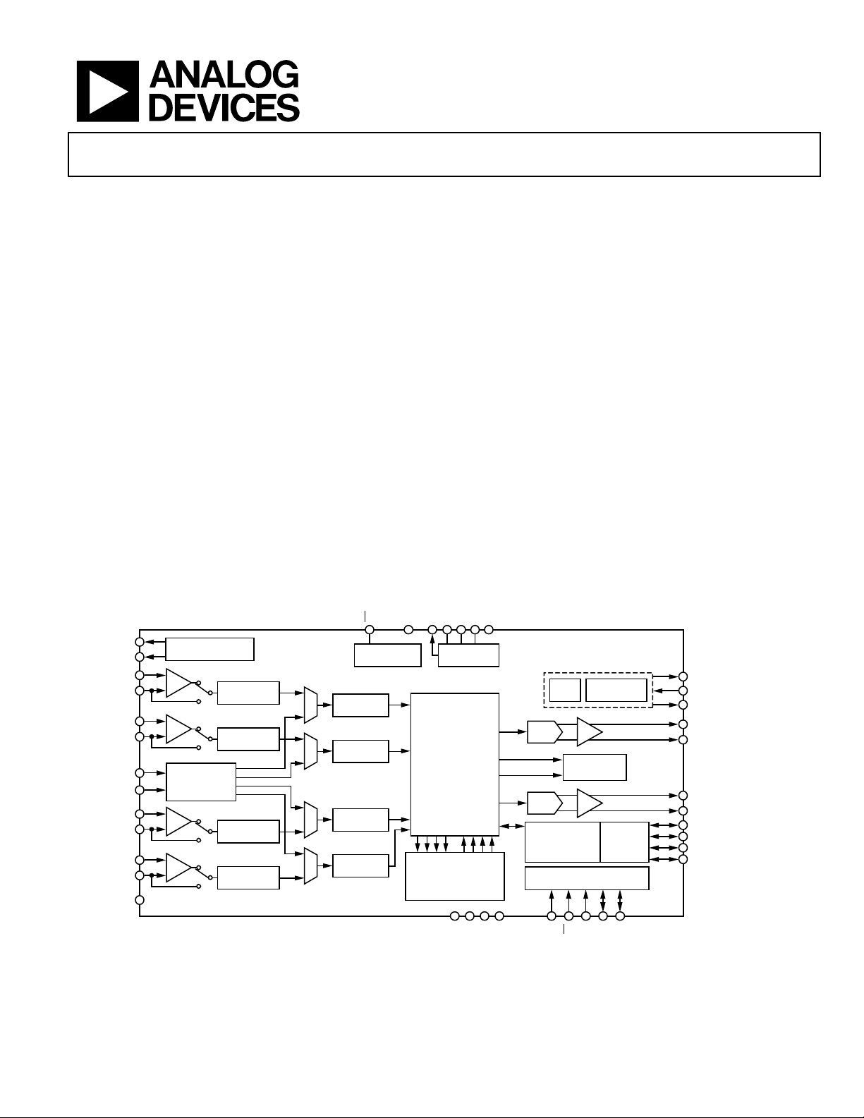
Four ADC, Two DAC Low Power Codec
with Audio Processor
ADAU1772
Rev. 0
third parties that may result from its use. Specifications subject to change without notice. No
Trademarks and registered trademarks are the prop erty of their respective owner s.
Fax: 781.461.3113 ©2012 Analog Devices, Inc. All rights reserved.
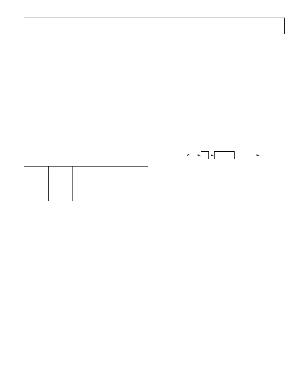
MICROPHONE
BIAS GENERATORS
MICBIAS0
MICBIAS1
CM
ADC
MODULATOR
ADC
DECIMATOR
AIN0REF
AIN0
PGA
ADC
MODULATOR
ADC
DECIMATOR
AIN1REF
AIN1
PGA
ADC
MODULATOR
AIN2REF
AIN2
PGA
ADC
MODULATOR
AIN3REF
AIN3
PGA
ADC
DECIMATOR
ADC
DECIMATOR
DMIC0_1/MP4
DMIC2_3/MP5
DIGITAL
MICROPHONE
INPUTS
INPUT/OUTPUT
SIGNAL
ROUTING
DSP CORE:
BIQUAD FILTERS,
LIMITERS,
VOLUME CONTROLS,
MIXING
I2C/SPI CONTROL
INTERFACE AND S E LF-BOOT
BIDIRECTIONAL
ASRCS
SERIAL
INPUT/
OUTPUT
PORT
LDO
REGULATOR
REG_OUT
AVDD
AVDD
AVDD
IOVDD
DVDD
POWER
MANAGEMENT
PD
PLL
CLOCK
OSCILLATOR
SELFBOOT
DGND
AGND
AGND
AGND
ADDR0/SS
ADDR1/MOSI
SCL/SCLK
SDA/MISO
DAC_SDATA/MP0
ADC_SDATA1/CLKOUT/MP6
XTALI/MCLKIN
XTALO
ADC_SDATA0/PDMOUT/MP1
BCLK/MP2
LRCLK/MP3
DAC
DAC
STEREO PDM
MODULATOR
ADAU1772
10804-001
HPOUTLP/LOUTLP
HPOUTLN/LOUTLN
HPOUTRP/LOUTRP
HPOUTRN/LOUTRN
Data Sheet
FEATURES
Programmable audio processing engine
192 kHz processing path
Biquad filters, limiters, volume controls, mixing
Low latency, 24-bit ADCs and DACs
102 dB SNR (signal through PGA and ADC
with A-weighted filter)
107 dB combined SNR (signal through DAC and headphone
with A-weighted filter)
Serial port sample rates from 8 kHz to 192 kHz
38 μs analog-to-analog latency
4 single-ended analog inputs—configurable as microphone
or line inputs
Dual stereo digital microphone inputs
Stereo analog audio output—single-ended or differential,
configurable as either line output or headphone driver
PLL supporting any input clock rate from 8 MHz to 27 MHz
Full-duplex, asynchronous sample rate converters (ASRCs)
Power supplies
Analog and digital I/O of 1.8 V to 3.3 V
Digital signal processing (DSP) core of 1.1 V to 1.8 V
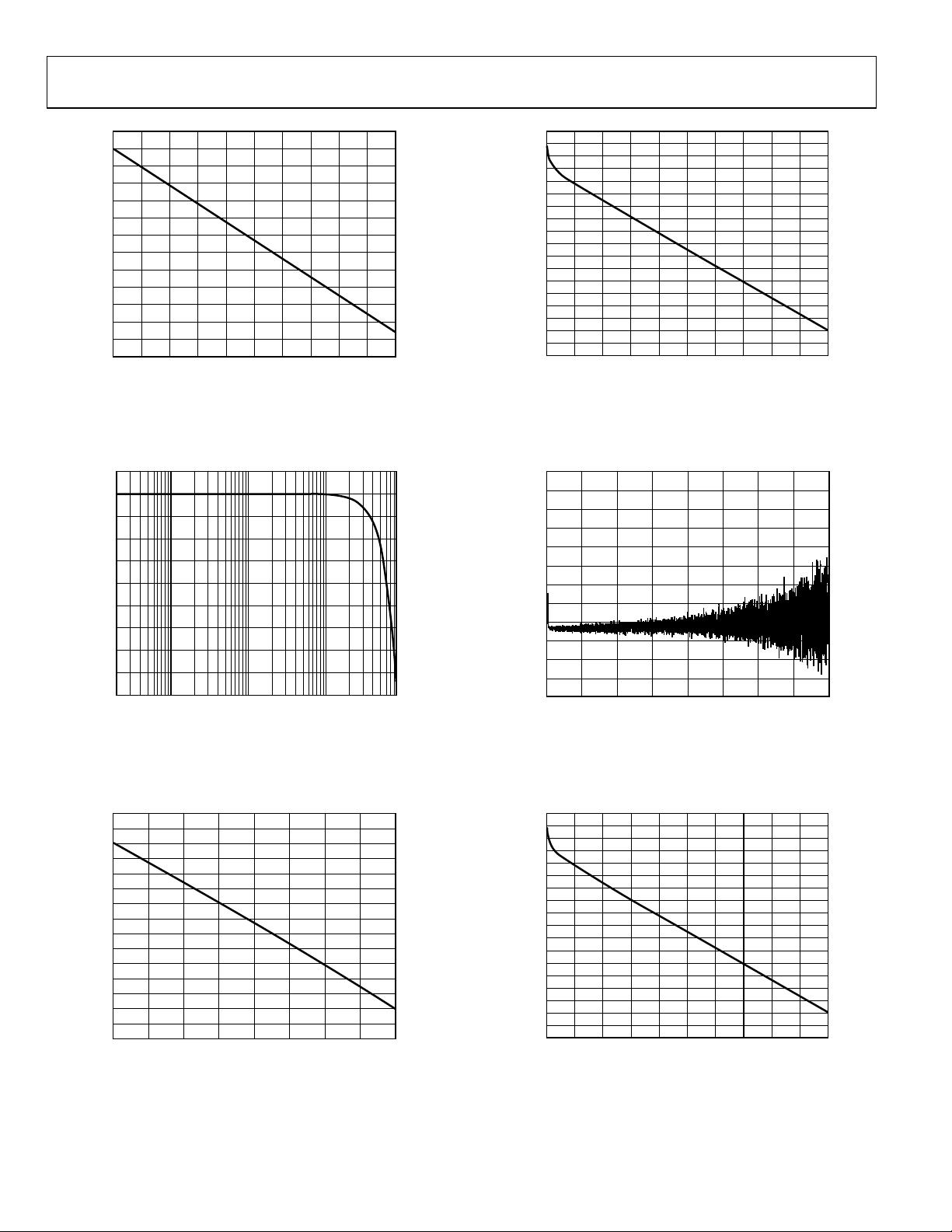
FUNCTIONAL BLOCK DIAGRAM
Low power (15 mW for typical noise cancelling solution)
2
I
C and SPI control interfaces, self-boot from I2C EEPROM
7 MP pins supporting dual stereo digital microphone inputs,
stereo PDM output, mute, DSP bypass, push-button
volume controls, and parameter bank switching
APPLICATIONS
Noise cancelling handsets, headsets, and headphones
Bluetooth ANC handsets, headsets, and headphones
Personal navigation devices
Digital still and video cameras
GENERAL DESCRIPTION
The ADAU1772 is a codec with four inputs and two outputs that
incorporates a digital processing engine to perform filtering,
level control, signal level monitoring, and mixing. The path
from the analog input to the DSP core to the analog output is
optimized for low latency and is ideal for noise cancelling headsets.
With the addition of just a few passive components, a crystal,
and an EEPROM for booting, the ADAU1772 provides a
complete headset solution.
Information furnished by Analog Devices is believed to be accurate and reliable. However, no
responsibility is assumed by Analog Devices for its use, nor for any infringements of patents or other
rights of
license is granted by implication or otherwise under any patent or patent rights of Analog Devices.
Figure 1.
One Technology Way, P.O. Box 9106, Norwood, MA 02062-9106, U.S.A.
Tel: 781.329.4700 www.analog.com
Page 2

ADAU1772 Data Sheet
TABLE OF CONTENTS
Features .............................................................................................. 1
Applications ....................................................................................... 1
General Description ......................................................................... 1
Functional Block Diagram .............................................................. 1
Revision History ............................................................................... 3
Specifications ..................................................................................... 4
Analog Performance Specifications ........................................... 4
Crystal Amplifier Specifications ................................................. 7
Digital Input/Output Specifications........................................... 8
Power Supply Specifications........................................................ 8
Typical Power Consumption ....................................................... 9
Digital Filters ................................................................................. 9
Digital Timing Specifications ................................................... 10
Absolute Maximum Ratings .......................................................... 14
Thermal Resistance .................................................................... 14
ESD Caution ................................................................................ 14
Pin Configuration and Function Descriptions ........................... 15
Typical Performance Characteristics ........................................... 17
System Block Diagrams ................................................................. 27
Theory of Operation ...................................................................... 28
System Clocking and Power-Up ................................................... 29
Clock Initialization ..................................................................... 29
PLL ............................................................................................... 29
Clock Output ............................................................................... 30
Power Sequencing ...................................................................... 30
Signal Routing ................................................................................. 31
Input Signal Paths ........................................................................... 32
Analog Inputs .............................................................................. 32
Digital Microphone Input ......................................................... 33
Analog-to-Digital Converters ................................................... 33
Output Signal Paths ........................................................................ 34
Analog Outputs........................................................................... 34
Digital-to-Analog Converters ................................................... 34
PDM Output ............................................................................... 34
Asynchronous Sample Rate Converters .................................. 35
Signal Levels ................................................................................ 35
Signal Processing ............................................................................ 36
Instructions ................................................................................. 36
Data Memory .............................................................................. 36
Parameters ................................................................................... 36
Control Port .................................................................................... 39
I2C Port ........................................................................................ 39
SPI Port ........................................................................................ 42
Self-Boot ...................................................................................... 43
Multipurpose Pins .......................................................................... 44
Push-Button Volume Controls ................................................. 44
Limiter Compression Enable .................................................... 44
Parameter Bank Switching ........................................................ 44
Mute ............................................................................................. 44
DSP Bypass Mode ...................................................................... 45
Serial Data Input/Output Ports .................................................... 46
Tristating Unused Channels...................................................... 46
Applications Information .............................................................. 49
Power Supply Bypass Capacitors .............................................. 49
Layout .......................................................................................... 49
Grounding ................................................................................... 49
Exposed Pad PCB Design ......................................................... 49
Register Summary .......................................................................... 50
Register Details ............................................................................... 52
Clock Control Register .............................................................. 52
PLL Denominator MSB Register .............................................. 53
PLL Denominator LSB Register ............................................... 53
PLL Numerator MSB Register .................................................. 53
PLL Numerator LSB Register .................................................... 54
PLL Integer Setting Register ..................................................... 54
PLL Lock Flag Register .............................................................. 55
CLKOUT Setting Selection Register ........................................ 55
Regulator Control Register ....................................................... 56
Core Control Register ................................................................ 57
Filter Engine and Limiter Control Register ............................ 58
DB Value Register 0 Read .......................................................... 59
DB Value Register 1 Read .......................................................... 59
DB Value Register 2 Read .......................................................... 60
Core Channel 0/Core Channel 1 Input Select Register ......... 61
Core Channel 2/Core Channel 3 Input Select Register ......... 62
DAC Input Select Register ........................................................ 63
PDM Modulator Input Select Register .................................... 64
Serial Data Output 0/Serial Data Output 1 Input Select
Register ........................................................................................ 65
Rev. 0 | Page 2 of 116
Page 3

Data Sheet ADAU1772
Serial Data Output 2/Serial Data Output 3 Input Select
Register ......................................................................................... 66
Serial Data Output 4/Serial Data Output 5 Input Select
Register ......................................................................................... 67
Serial Data Output 6/Serial Data Output 7 Input Select
Register ......................................................................................... 68
ADC_SDATA0/ADC_SDATA1 Channel Select Register ...... 69
Output ASRC0/Output ASRC1 Source Register ..................... 70
Output ASRC2/Output ASRC3 Source Register ..................... 71
Input ASRC Channel Select Register ........................................ 72
ADC0/ADC1 Control 0 Register .............................................. 73
ADC2/ADC3 Control 0 Register .............................................. 74
ADC0/ADC1 Control 1 Register .............................................. 75
ADC2/ADC3 Control 1 Register .............................................. 76
ADC0 Volume Control Register ............................................... 77
ADC1 Volume Control Register ............................................... 77
ADC2 Volume Control Register ............................................... 78
ADC3 Volume Control Register ............................................... 78
PGA Control 0 Register .............................................................. 79
PGA Control 1 Register .............................................................. 79
PGA Control 2 Register .............................................................. 80
PGA Control 3 Register .............................................................. 81
PGA Slew Control Register ........................................................ 82
PGA 10 dB Gain Boost Register ................................................ 83
Input and Output Capacitor Charging Register ..................... 84
DSP Bypass Path Register .......................................................... 85
DSP Bypass Gain for PGA0 Register ........................................ 85
DSP Bypass Gain for PGA1 Register ........................................ 85
MIC_BIAS0_1 Control Register ............................................... 86
DAC Control Register ................................................................ 86
DAC0 Volume Control Register ................................................ 87
DAC1 Volume Control Register ................................................ 87
Headphone Output Mutes Register .......................................... 88
Serial Port Control 0 Register .................................................... 89
Serial Port Control 1 Register .................................................... 90
TDM Output Channel Disable Register .................................. 91
PDM Enable Register ................................................................. 92
PDM Pattern Setting Register ................................................... 93
MP0 Function Setting Register ................................................. 93
MP1 Function Setting Register ................................................. 94
MP2 Function Setting Register ................................................. 95
MP3 Function Setting Register ................................................. 96
MP4 Function Setting Register ................................................. 97
MP5 Function Setting Register ................................................. 98
MP6 Function Setting Register ................................................. 99
Push-Button Volume Settings Register .................................. 100
Push-Button Volume Control Assignment Register ............ 101
Debounce Modes Register ....................................................... 102
Headphone Line Output Select Register ................................ 102
Decimator Power Control Register ........................................ 104
ASRC Interpolator and DAC Modulator Power Control
Register ....................................................................................... 105
Analog Bias Control 0 Register ............................................... 105
Analog Bias Control 1 Register ............................................... 106
Digital Pin Pull-Up Control 0 Register .................................. 107
Digital Pin Pull-Up Control 1 Register .................................. 108
Digital Pin Pull-Down Control 0 Register ............................ 109
Digital Pin Pull-Down Control 1 Register ............................ 110
Digital Pin Drive Strength Control 0 Register ...................... 111
Digital Pin Drive Strength Control 1 Register ...................... 112
Outline Dimensions ...................................................................... 113
Ordering Guide ......................................................................... 113
REVISION HISTORY
7/12—Revision 0: Initial Version
Rev. 0 | Page 3 of 116
Page 4

ADAU1772 Data Sheet
Parameter
Test Conditions/Comments
Min
Typ
Max
Unit
Single-Ended Line Input
0 dB gain
14.3 kΩ
AVDD = 1.8 V
−90 dB
AVDD = 1.8 V
0.49 V rms
SPECIFICATIONS
Master clock = core clock = 12.288 MHz, serial input sample rate = 48 kHz, measurement bandwidth = 20 Hz to 20 kHz, word width =
24 bits, ambient temperature = 25°C, outputs line loaded with 10 kΩ.
ANALOG PERFORMANCE SPECIFICATIONS
Supply voltages AVDD = IOVDD = 1.8 V, DVDD = 1.1 V, unless otherwise noted. PLL disabled, direct master clock.
Table 1.
ANALOG-TO-DIGITAL CONVERTERS
ADC Resolution All ADCs 24 Bits
Digital Attenuation Step 0.375 dB
Digital Attenuation Range 95 dB
INPUT RESISTANCE Gain settings do not include 10 dB gain from
PGA Inputs −12 dB gain 32.0 kΩ
0 dB gain 20 kΩ
+35.25 dB gain 0.68 kΩ
SINGLE-ENDED LINE INPUT PGA_ENx = 0, PGA_x_BOOST = 0, PGA_POP_DISx = 1
Full-Scale Input Voltage Scales linearly with AVDD AVDD/3.63 V rms
AVDD = 1.8 V 0.49 V rms
AVDD = 1.8 V, 0 dBFS 1.38 V p-p
AVDD = 3.3 V 0.90 V rms
AVDD = 3.3 V, 0 dBFS 2.54 V p-p
Dynamic Range
With A-Weighted Filter (RMS) AVDD = 1.8 V 97 dB
AVDD = 3.3 V 102 dB
With Flat 20 Hz to 20 kHz Filter AVDD = 1.8 V 94 dB
AVDD = 3.3 V 99 dB
Signal-to-Noise Ratio (SNR)
With A-Weighted Filter (RMS) AVDD = 1.8 V 98 dB
AVDD = 3.3 V 103 dB
With Flat 20 Hz to 20 kHz Filter AVDD = 1.8 V 96 dB
AVDD = 3.3 V 100 dB
Interchannel Gain Mismatch 40 mdB
Total Harmonic Distortion + Noise (THD + N) 20 Hz to 20 kHz, −1 dBFS
1
2
PGA_x_BOOST settings; this additional gain does
not affect input impedance; PGA_POP_DISx = 1
20 Hz to 20 kHz, −60 dB input
AVDD = 3.3 V −94 dB
Offset Error ±0.1 mV
Gain Error ±0.2 dB
Interchannel Isolation CM capacitor = 22 μF 100 dB
Power Supply Rejection Ratio CM capacitor = 22 μF
100 mV p-p at 1 kHz 55 dB
SINGLE-ENDED PGA INPUT PGA_ENx = 1, PGA_x_BOOST = 0
Full-Scale Input Voltage Scales linearly with AVDD AVDD/3.63 V rms
AVDD = 1.8 V, 0 dBFS 1.38 V p-p
AVDD = 3.3 V 0.90 V rms
AVDD = 3.3 V, 0 dBFS 2.54 V p-p
Dynamic Range
With A-Weighted Filter (RMS) AVDD = 1.8 V 96 dB
AVDD = 3.3 V 102 dB
With Flat 20 Hz to 20 kHz Filter AVDD = 1.8 V 94 dB
AVDD = 3.3 V 99 dB
1
20 Hz to 20 kHz, −60 dB input
Rev. 0 | Page 4 of 116
Page 5

Data Sheet ADAU1772
Interchannel Isolation
83 dB
Output Impedance
1 Ω
Parameter Test Conditions/Comments Min Typ Max Unit
Total Harmonic Distortion + Noise 20 Hz to 20 kHz, −1 dBFS
AVDD = 1.8 V −88 dB
AVDD = 3.3 V −90 dB
Signal-to-Noise Ratio
With A-Weighted Filter (RMS) AVDD = 1.8 V 96 dB
AVDD = 3.3 V 102 dB
With Flat 20 Hz to 20 kHz Filter AVDD = 1.8 V 94 dB
AVDD = 3.3 V 99 dB
PGA Gain Variation
With −12 dB Setting Standard deviation 0.05 dB
With +35.25 dB Setting Standard deviation 0.15 dB
PGA Boost PGA_x_BOOST 10 dB
PGA Mute Attenuation PGA_MUTEx −65 dB
Interchannel Gain Mismatch 0.005 dB
Offset Error 0 mV
Gain Error ±0.2 dB
Power Supply Rejection Ratio CM capacitor = 22 μF, 100 mV p-p at 1 kHz 63 dB
MICROPHONE BIAS MIC_ENx = 1
Bias Voltage
0.65 × AVDD AVDD = 1.8 V, MIC_GAINx = 1 1.16 V
AVDD = 3.3 V, MIC_GAINx = 1 2.12 V
0.90 × AVDD AVDD = 1.8 V, MIC_GAINx = 0 1.63 V
AVDD = 3.3 V, MIC_GAINx = 0 2.97 V
Bias Current Source 3 mA
2
MICBIASx Isolation MIC_GAINx = 0 95 dB
MIC_GAINx = 1 99 dB
Noise in the Signal Bandwidth3 AVDD = 1.8 V, 20 Hz to 20 kHz
MIC_GAINx = 0 27 nV/√Hz
MIC_GAINx = 1 16 nV/√Hz
AVDD = 3.3 V, 20 Hz to 20 kHz
MIC_GAINx = 0 35 nV/√Hz
MIC_GAINx = 1 19 nV/√Hz
DIGITAL-TO-ANALOG CONVERTERS
DAC Resolution All DACs 24 Bits
Digital Attenuation Step 0.375 dB
Digital Attenuation Range 95 dB
DAC SINGLE-ENDED OUTPUT Single-ended operation, HPOUTLP and
HPOUTRP pins
Full-Scale Output Voltage Scales linearly with AVDD AVDD/3.4 V rms
AVDD = 1.8 V 0.53 V rms
AVDD = 1.8 V, 0 dBFS 1.5 V p-p
AVDD = 3.3 V 0.97 V rms
AVDD = 3.3 V, 0 dBFS 2.74 V p-p
Mute Attenuation −72 dB
Dynamic Range
1
Line output mode, 20 Hz to 20 kHz, −60 dB input
With A-Weighted Filter (RMS) AVDD = 1.8 V 100 dB
AVDD = 3.3 V 104 dB
With Flat 20 Hz to 20 kHz Filter AVDD = 1.8 V 97 dB
AVDD = 3.3 V 101 dB
Signal-to-Noise Ratio
2
Line output mode, 20 Hz to 20 kHz
With A-Weighted Filter (RMS) AVDD = 1.8 V 100 dB
AVDD = 3.3 V 104 dB
With Flat 20 Hz to 20 kHz Filter AVDD = 1.8 V 98 dB
AVDD = 3.3 V 102 dB
Rev. 0 | Page 5 of 116
Page 6

ADAU1772 Data Sheet
AVDD = 3.3 V, <0.1% THD + N
28.1 mW
With A-Weighted Filter (RMS)
AVDD = 1.8 V
105 dB
Parameter Test Conditions/Comments Min Typ Max Unit
Interchannel Gain Mismatch Line output mode 20 mdB
Total Harmonic Distortion + Noise Line output mode, 20 Hz to 20 kHz, −1 dBFS dB
AVDD = 1.8 V −93 dB
AVDD = 3.3 V −94 dB
Gain Error Line output mode ±0.1 dB
Dynamic Range
With A-Weighted Filter (RMS) AVDD = 1.8 V 100 dB
AVDD = 3.3 V 104 dB
With Flat 20 Hz to 20 kHz Filter AVDD = 1.8 V 97 dB
AVDD = 3.3 V 101 dB
Signal-to-Noise Ratio
With A-Weighted Filter (RMS) AVDD = 1.8 V 100 dB
AVDD = 3.3 V 104 dB
With Flat 20 Hz to 20 kHz Filter AVDD = 1.8 V 98 dB
AVDD = 3.3 V 102 dB
Interchannel Gain Mismatch Headphone mode 50 mdB
Total Harmonic Distortion + Noise Headphone mode, 20 Hz to 20 kHz, −1 dBFS
32 Ω load AVDD = 1.8 V, PO = 6.7 mW −77 dB
AVDD = 3.3 V, PO = 22.4 mW −80 dB
24 Ω load AVDD = 1.8 V, PO = 8.9 mW −76 dB
AVDD = 3.3 V, PO = 30 mW −79 dB
16 Ω load AVDD = 1.8 V, PO = 13 mW −74 dB
AVDD = 3.3 V, PO = 44 mW −77 dB
Headphone Output Power
32 Ω Load AVDD = 1.8 V, <0.1% THD + N 8.4 mW
1
2
Headphone mode, 20 Hz to 20 kHz, −60 dB input
Headphone mode, 20 Hz to 20 kHz
24 Ω Load AVDD = 1.8 V, <0.1% THD + N 11.2 mW
AVDD = 3.3 V, <0.1% THD + N 37.4 mW
16 Ω Load AVDD = 1.8 V, <0.1% THD + N 16.25 mW
AVDD = 3.3 V, <0.1% THD + N 55.8 mW
Gain Error Headphone mode ±0.1 dB
Offset Error ±0.1 mV
Interchannel Isolation 1 kHz, 0 dBFS input signal 100 dB
Power Supply Rejection Ratio CM capacitor = 22 μF, 100 mV p-p at 1 kHz 70 dB
DAC DIFFERENTIAL OUTPUT Differential operation
Full-Scale Output Voltage Scales linearly with AVDD AVDD/1.8 V rms
AVDD = 1.8 V 1.0 V rms
AVDD = 1.8 V, 0 dBFS 2.58 V p-p
AVDD = 3.3 V 1.83 V rms
AVDD = 3.3 V, 0 dBFS 5.49 V p-p
Mute Attenuation −72 dB
Dynamic Range
1
Line output mode, 20 Hz to 20 kHz, −60 dB input
With A-Weighted Filter (RMS) AVDD = 1.8 V 104 dB
AVDD = 3.3 V 107 dB
With Flat 20 Hz to 20 kHz Filter AVDD = 1.8 V 101 dB
AVDD = 3.3 V 105 dB
Signal-to-Noise Ratio
2
Line output mode, 20 Hz to 20 kHz
AVDD = 3.3 V 108 dB
With Flat 20 Hz to 20 kHz Filter AVDD = 1.8 V 102 dB
AVDD = 3.3 V 105 dB
Interchannel Gain Mismatch Line output mode 20 mdB
Total Harmonic Distortion + Noise Line output mode, 20 Hz to 20 kHz, −1 dBFS dB
AVDD = 1.8 V −96 dB
AVDD = 3.3 V −96 dB
Gain Error Line output mode %
Rev. 0 | Page 6 of 116
Page 7

Data Sheet ADAU1772
16 Ω Load
−3 dBFS, AVDD = 1.8 V, PO = 33 mW
−75 dB
Parameter
Jitter
270
500
ps
Parameter Test Conditions/Comments Min Typ Max Unit
Dynamic Range
With A-Weighted Filter (RMS) AVDD = 1.8 V 104 dB
AVDD = 3.3 V 107 dB
With Flat 20 Hz to 20 kHz Filter AVDD = 1.8 V 102 dB
AVDD = 3.3 V 104 dB
Signal-to-Noise Ratio
With A-Weighted Filter (RMS) AVDD = 1.8 V 105 dB
AVDD = 3.3 V 108 dB
With Flat 20 Hz to 20 kHz Filter AVDD = 1.8 V 103 dB
AVDD = 3.3 V 106 dB
Interchannel Gain Mismatch Headphone mode 75 mdB
Total Harmonic Distortion + Noise Headphone mode
32 Ω Load −1 dBFS, AVDD = 1.8 V, PO = 27 mW −75 dB
−1 dBFS, AVDD = 3.3 V, PO = 90 mW −83 dB
24 Ω Load −2 dBFS, AVDD = 1.8 V, PO = 28 mW −75 dB
−1 dBFS, AVDD = 3.3 V, PO = 118 mW −77 dB
−1 dBFS, AVDD = 3.3 V, PO = 175 mW −83 dB
Headphone Output Power
32 Ω Load AVDD = 1.8 V, <0.1% THD + N 32.5 mW
AVDD = 3.3 V, <0.1% THD + N 111.8 mW
24 Ω Load AVDD = 1.8 V, <0.1% THD + N 37.6 mW
AVDD = 3.3 V, <0.1% THD + N 148.3 mW
16 Ω Load AVDD = 1.8 V, <0.1% THD + N 41.5 mW
AVDD = 3.3 V, <0.1% THD + N 189.2 mW
Gain Error Headphone mode ±0.25 %
Offset Error ±0.1 mV
Interchannel Isolation 1 kHz, 0 dBFS input signal 100 dB
Power Supply Rejection Ratio CM capacitor = 22 μF
100 mV p-p at 1 kHz 73 dB
CM REFERENCE CM pin
Common-Mode Reference Output AVDD/2 V
Common-Mode Source Impedance 5 kΩ
REGULATOR
Line Regulation 1 mV/V
Load Regulation 6 mV/mA
1
Dynamic range is the ratio of the sum of noise and harmonic power in the band of interest with a −60 dBFS signal present to the full-scale power level in decibels.
2
SNR is the ratio of the sum of all noise power in the band of interest with no signal present to the full-scale power level in decibels.
3
These specifications are with 4.7 µF decoupling and 5.0 kΩ load on pin.
CRYSTAL AMPLIFIER SPECIFICATIONS
Supply voltages AVDD = IOVDD = 1.8 V, DVDD = 1.1 V, unless otherwise noted.
1
2
Headphone mode, 20 Hz to 20 kHz, −60 dB input
Headphone mode, 20 Hz to 20 kHz
Table 2.
Frequency Range 8 27 MHz
Load Capacitance 20 pF
Test Conditions/Comments Min Typ Max Unit
Rev. 0 | Page 7 of 116
Page 8

ADAU1772 Data Sheet
IIL at VIL = 0.8 V
10
µA
Digital I/O Current with IOVDD = 1.8 V
Crystal oscillator enabled
fS = 8 kHz
0.35 mA
fS = 8 kHz
1.99 mA
DIGITAL INPUT/OUTPUT SPECIFICATIONS
−40°C < TA < +85°C, IOVDD = 3.3 V ± 10% and 1.8 V − 5%/+10%.
Table 3.
Parameter Test Conditions/Comments Min Typ Max Unit
Input Voltage High (VIH) IOVDD = 3.3 V 2.0 V
IOVDD = 1.8 V 1.1 V
Input Voltage Low (VIL) IOVDD = 3.3 V 0.8 V
IOVDD = 1.8 V 0.45 V
Input Leakage IOVDD = 3.3 V, IIH at VIH = 2.0 V 10 µA
IOVDD = 1.8 V, IIH at VIH = 1.1 V 10 µA
IIL at VIL = 0.45 V 10 µA
Output Voltage High (VOH) with Low Drive Strength IOH = 1 mA IOVDD − 0.6 V
Output Voltage High (VOH) with High Drive Strength IOH = 3 mA IOVDD − 0.6 V
Output Voltage Low (VOL) with Low Drive Strength IOL = 1 mA 0.4 V
Output Voltage Low (VOL) with High Drive Strength IOL = 3 mA 0.4 V
Input Capacitance 5 pF
POWER SUPPLY SPECIFICATIONS
Supply voltages AVDD = IOVDD = 1.8 V, DVDD = 1.1 V, unless otherwise noted. PLL disabled, direct master clock.
Table 4.
Parameter Test Conditions/Comments Min Typ Max Unit
SUPPLIES
AVDD Voltage 1.71 1.8 3.63 V
DVDD Voltage 1.045 1.1 1.98 V
IOVDD Voltage 1.71 1.8 3.63 V
Slave Mode fS = 48 kHz 0.35 mA
fS = 192 kHz 0.49 mA
fS = 8 kHz 0.32 mA
Master Mode fS = 48 kHz 0.53 mA
fS = 192 kHz 1.18 mA
Power-Down 0 µA
Digital I/O Current with IOVDD = 3.3 V Crystal oscillator enabled
Slave Mode fS = 48 kHz 2.05 mA
fS = 192 kHz 2.28 mA
Master Mode fS = 48 kHz 2.4 mA
fS = 192 kHz 3.62 mA
fS = 8 kHz 2.05 mA
Power-Down 7 µA
Analog Current (AVDD) See Table 5
Power-Down AVDD = 1.8 V 0.6 µA
AVDD = 3.3 V 13.6 µA
DISSIPATION
Operation fS = 192 kHz (see conditions in Table 5)
All Supplies 15.5 mW
Digital I/O Supply 0.7 mW
Analog Supply Includes regulated DVDD current 14.8 mW
Power-Down, All Supplies 1 µW
Rev. 0 | Page 8 of 116
Page 9
Data Sheet ADAU1772
Enhanced performance
12.65
−93
−90.5
Power saving
7.78
−84.5
−87.5
Dynamic Range
100 dB
PDM MODULATOR
TYPICAL POWER CONSUMPTION
Typical active noise cancelling (ANC) settings. Master clock = 12.288 MHz, fS = 192 kHz. On-board regulator enabled. Two analog-todigital converters (ADCs) with PGA enabled and two ADCs configured for line input; no input signal. Two digital-to-analog converters
(DACs) configured for differential headphone operation; DAC outputs unloaded. Both MICBIAS0 and MICBIAS1 enabled. ASRCs and
pulse density modulated (PDM) modulator disabled. Core running 26 out of 32 possible instructions. For total power consumption, add
IOVDD at 8 kHz slave current listed in Tabl e 4.
Table 5.
Typical AVDD Power Consumption
Operating Voltage Power Management Setting
AVDD = IOVDD = 3.3 V Normal (default) 11.5 −93 −87.5
Extreme power saving 9.4 −93 −86.5
Power saving 9.8 −93 −86.5
AVDD = IOVDD = 1.8 V Normal (default) 9.37 −86 −91
Extreme power saving 7.40 −84.5 −87
Enhanced performance 10.4 −86 −94.5
(mA)
DIGITAL FILTERS
Table 6.
Parameter Test Conditions/Comments Min Typ Max Unit
ADC INPUT TO DAC OUTPUT PATH
Pass-Band Ripple DC to 20 kHz, fS = 192 kHz ±0.02 dB
Group Delay fS = 192 kHz 38 µs
SAMPLE RATE CONVERTER
Pass Band LRCLK < 63 kHz 0 0.475 × fS kHz
63 kHz < LRCLK <130 kHz 0 0.4286 × fS
LRCLK > 130 kHz 0 0.4286 × fS
Pass-Band Ripple Upsampling, 96 kHz −0.27 0.05 dB
Upsampling, 192 kHz −0.06 0.05 dB
Downsampling, 96 kHz 0 0.07 dB
Downsampling, 192 kHz 0 0.07 dB
Input/Output Frequency Range 8 192 kHz
Typical ADC THD + N
(dB)
Typical HP Output
THD + N (dB)
Total Harmonic Distortion + Noise −90 dB
Startup Time 15 ms
Dynamic Range (A-Weighted) 112 dB
Total Harmonic Distortion + Noise −92 dB
Rev. 0 | Page 9 of 116
Page 10

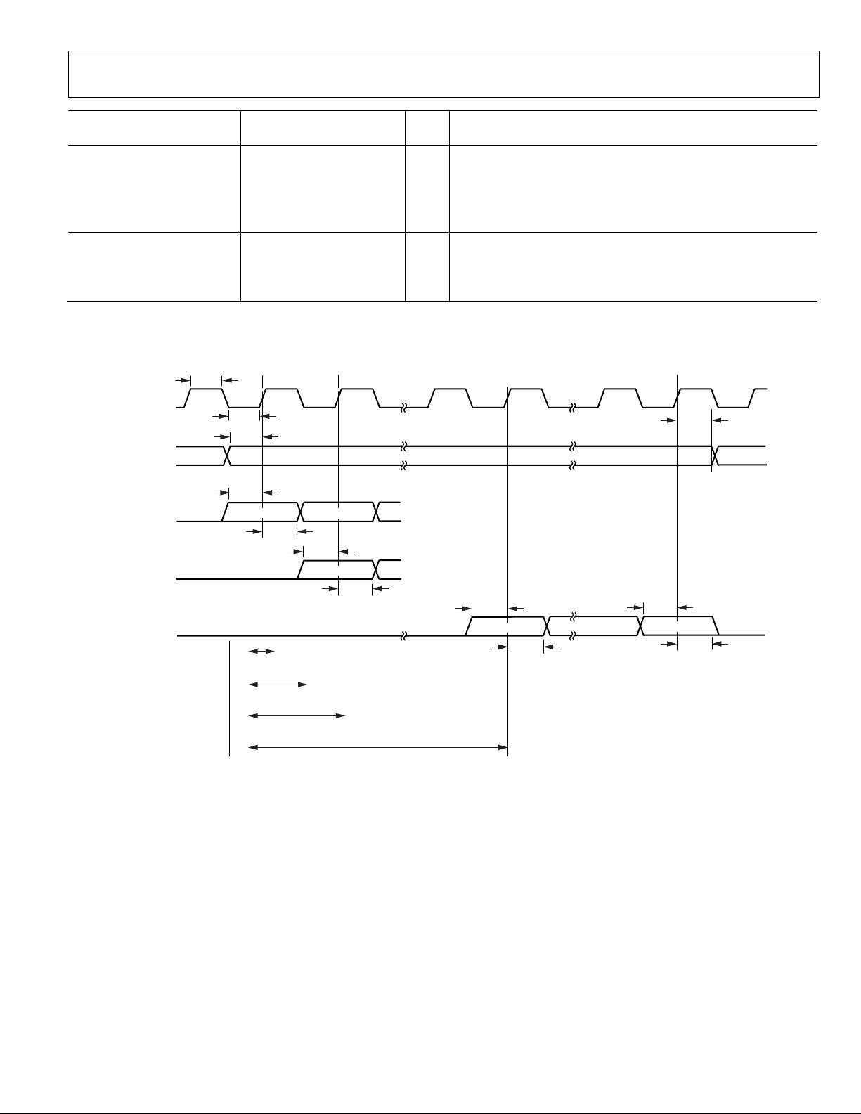
ADAU1772 Data Sheet
tLS
10 ns
LRCLK setup; time to BCLK rising (slave mode)
t
30
ns
BCLK falling to ADC_SDATAx driven in TDM tristate mode
t
80 ns
SS pulse width high
t
250
ns
SDA fall time; C
= 400 pF
t
6 × tMP – 70
ns
Delay from SCL falling to SDA changing
MULTIPURPOSE AND POWER-
DIGITAL TIMING SPECIFICATIONS
−40°C < TA < +85°C, IOVDD = 1.71 V to 3.63 V, DVDD = 1.045 V to 1.98 V.
Table 7. Digital Timing
Limit
Parameter T
MASTER CLOCK
tMP 37 125 ns MCLKIN period; 8 MHz to 27 MHz input clock using PLL
t
77 82 ns Internal MCLK period; direct MCLK and PLL output divided by 2
MCLK
SERIAL PORT
tBL 40 ns BCLK low pulse width (master and slave modes)
tBH 40 ns BCLK high pulse width (master and slave modes)
tLH 10 ns LRCLK hold; time from BCLK rising (slave mode)
tSS 5 ns DAC_SDATA setup; time to BCLK rising (master and slave modes)
tSH 5 ns DAC_SDATA hold; time from BCLK rising (master and slave modes)
tTS 10 ns BCLK falling to LRCLK timing skew (master mode)
t
0 34 ns ADC_SDATAx delay; time from BCLK falling (master and slave modes)
SOD
SOTD
t
30 ns BCLK falling to ADC_SDATAx tristated in TDM tristate mode
SOTX
SPI PORT
f
SCLK
t
80 ns SCLK pulse width low
CCPL
t
80 ns SCLK pulse width high
CCPH
t
5 ns SS setup; time to SCLK rising
CLS
t
100 ns SS hold; time from SCLK rising
CLH
CLPH
t
10 ns MOSI setup; time to SCLK rising
CDS
t
10 ns MOSI hold; time from SCLK rising
CDH
t
101 ns MISO delay; time from SCLK falling
COD
I2C PORT
f
SCL
t
0.6 µs SCL high
SCLH
t
1.3 µs SCL low
SCLL
t
0.6 µs
SCS
t
250 ns SCL and SDA rise time, C
SCR
t
0.6 µs SCL fall hold time (from SDA falling), relevant for start condition
SCH
tDS 100 ns SDA setup time (to SCL rising)
t
250 ns SCL fall time; C
SCF
SDF
t
0.6 µs SCL rise setup time (to SDA rising), relevant for stop condition
BFT
I2C EEPROM SELF-BOOT
t
26 × tMP – 70 ns
SCHE
t
38 × tMP – 70 ns
SCSE
t
70 × tMP – 70 ns SCL rise setup time (to SDA rising), relevant for stop condition
BFTE
DSE
t
32 × tMP ns
BHTE
T
MIN
Unit Description
MAX
6.25 MHz SCLK frequency
400 kHz SCL frequency
SCL rise setup time (to SDA falling), relevant for repeated start
condition
SCL fall hold time (from SDA falling), relevant for start condition; t
is the input clock on the MCLKIN pin
SCL rise setup time (to SDA falling), relevant for repeated start
condition
SDA rising in self-boot stop condition to SDA falling edge for
external master start condition
= 400 pF
LOAD
LOAD
= 400 pF
LOAD
MP
DOWN PINS
t
1.5 × 1/f
GIL
t
20 ns
RLPW
µs MPx input latency; time until high or low value is read by core
S
PD low pulse width
Rev. 0 | Page 10 of 116
Page 11
Data Sheet ADAU1772
DIGITAL MICROPHONE
t
0
30
ns
PDM delay time for valid data
BCLK
LRCLK
DAC_SDATA
LEFT-JUSTIFIED
MODE
LSB
DAC_SDATA
I
2
S MODE
DAC_SDATA
RIGHT-JUSTIFIED
MODE
t
BH
MSB
MSB – 1
MSB
MSB
8-BIT CLOCKS
(24-BIT DAT A)
12-BIT CLOCKS
(20-BIT DAT A)
14-BIT CLOCKS
(18-BIT DAT A)
16-BIT CLOCKS
(16-BIT DAT A)
t
LS
t
SS
t
SH
t
SH
t
SS
t
SS
t
SH
t
SS
t
SH
t
LH
t
BL
10804-002
Limit
Parameter T
tCF 20 ns Digital microphone clock fall time
tCR 20 ns Digital microphone clock rise time
tDS 40 Digital microphone valid data start time
tDE 0 ns Digital microphone valid data end time
PDM OUTPUT
t
20 ns PDM clock fall time
DCF
t
20 ns PDM clock rise time
DCR
DDV
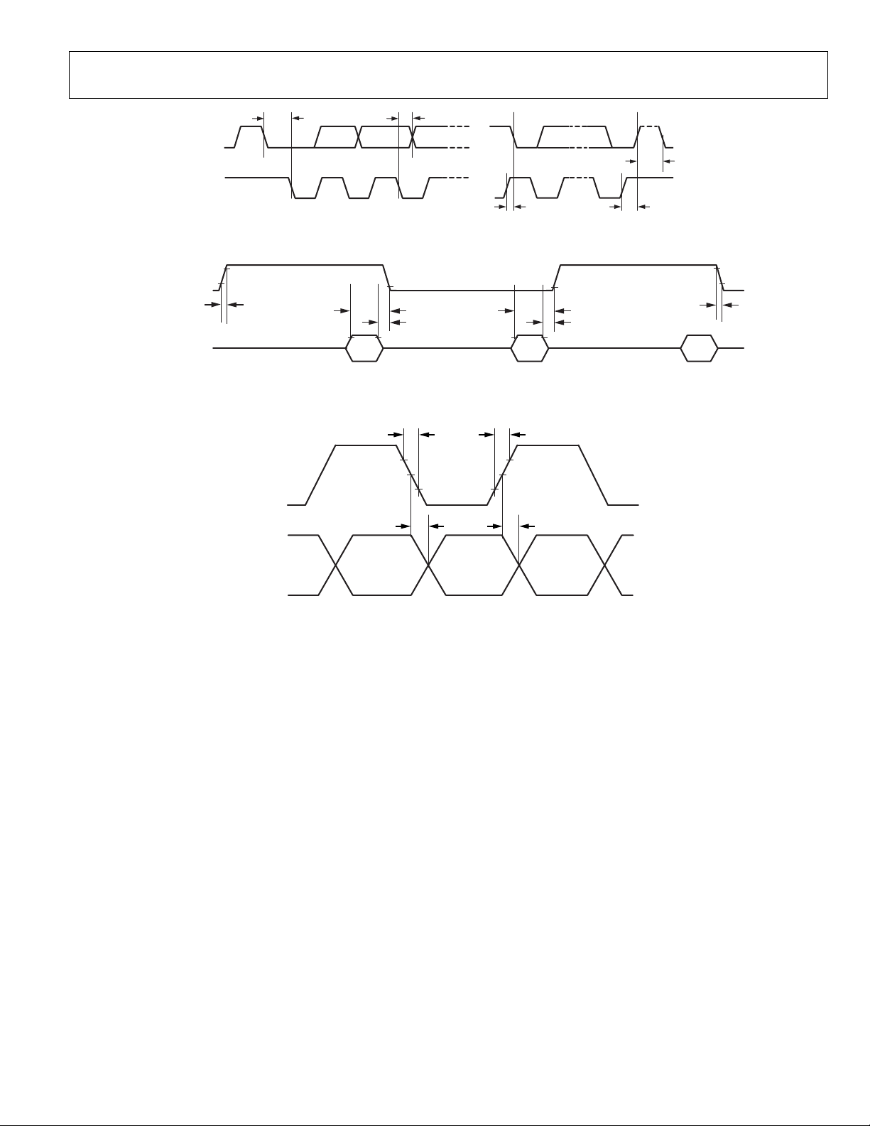
Digital Timing Diagrams
T
MIN
Unit Description
MAX
Figure 2. Serial Input Port Timing
Rev. 0 | Page 11 of 116
Page 12
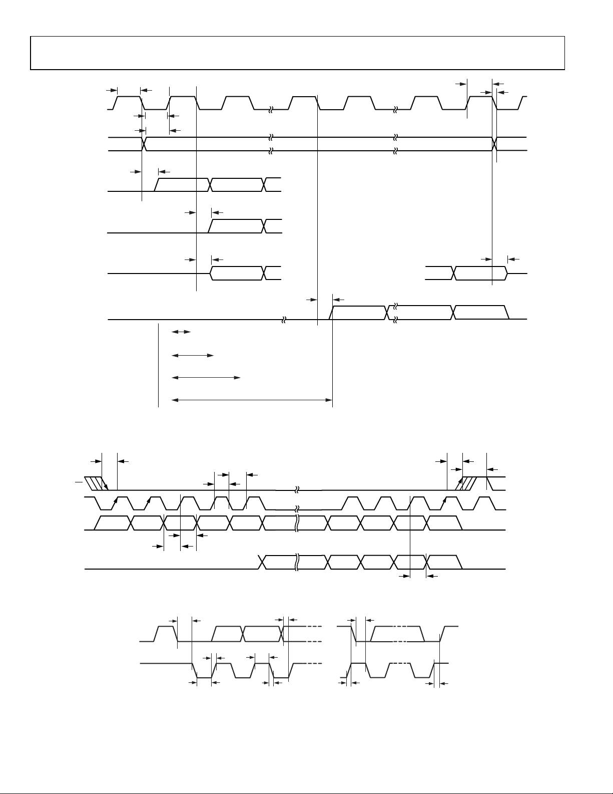
ADAU1772 Data Sheet
LRCLK
LSB
ADC_SDATAx
I
2
S MODE
ADC_SDATAx
RIGHT-JUSTIFIED
MODE
MSB
ADC_SDATAx
LEFT-JUSTIFIED
MODE
MSB
MSB – 1
ADC_SDATAx
W/TRISTATE MSB
LSB
MSB
8-BIT CLOCKS
(24-BIT DAT A)
12-BIT CLOCKS
(20-BIT DAT A)
14-BIT CLOCKS
(18-BIT DAT A)
16-BIT CLOCKS
(16-BIT DAT A)
t
LS
t
SOD
t
SOD
t
SOTD
t
SOD
t
SOTX
t
LH
t
TS
t
BL
BCLK
t
BH
HIGH-Z HIGH-Z
10804-003
SS
SCLK
MOSI
MISO
t
CLS
t
CDS
t
CDH
t
COD
t
CCPH
t
CCPL
t
CLH
t
CLPH
10804-004
t
SCH
t
SCLH
t
SCR
t
SCLL
t
SCF
t
DS
SDA
SCL
t
SCH
t
BFT
t
SCS
10804-005
Figure 3. Serial Output Port Timing
Figure 4. SPI Port Timing
Figure 5. I
2
C Port Timing
Rev. 0 | Page 12 of 116
Page 13
Data Sheet ADAU1772
t
SCHE
t
DSE
t
SCSE
t
BFTE
t
BHTE
SDA
SCL
10804-006
DMIC0_1/DMIC2_3
VALID LEFT SAMPLE VALID LEFT SAMPLEVALID RIGHT SAMPLE
CLKOUT
t
CR
t
CF
t
DS
t
DE
t
DS
t
DE
10804-007
t
DCF
PDMOUT
CLKOUT
RIGHT LEFT RIGHT LEFT
t
DCR
t
DDV
t
DDV
10804-008
Figure 6. I
2
C Self-Boot Timing
Figure 7. Digital Microphone Timing
Figure 8. PDM Output Timing
Rev. 0 | Page 13 of 116
Page 14
ADAU1772 Data Sheet
Digital Supply (DVDD)
−0.3 V to +1.98 V
40-Lead LFCSP
29
1.8
°C/W
ABSOLUTE MAXIMUM RATINGS
Table 8.
Parameter Rating
Power Supply (AVDD, IOVDD) −0.3 V to +3.63 V
Input Current (Except Supply Pins) ±20 mA
Analog Input Voltage (Signal Pins) –0.3 V to AVDD + 0.3 V
Digital Input Voltage (Signal Pins) −0.3 to IOVDD + 0.3 V
Operating Temperature Range (Case) −40°C to +85°C
Storage Temperature Range −65°C to +150°C
Stresses above those listed under Absolute Maximum Ratings
may cause permanent damage to the device. This is a stress
rating only; functional operation of the device at these or any
other conditions above those indicated in the operational
section of this specification is not implied. Exposure to absolute
maximum rating conditions for extended periods may affect
device reliability.
THERMAL RESISTANCE
θ
represents the junction-to-ambient thermal resistance; θ
JA
represents the junction-to-case thermal resistance. Thermal
numbers are simulated on a 4-layer JEDEC PCB with the
exposed pad soldered to the PCB. θ
was simulated at the
JC
exposed pad on the bottom of the package.
Table 9. Thermal Resistance
Package Type θ
JA
θ
JC
Unit
ESD CAUTION
JC
Rev. 0 | Page 14 of 116
Page 15

Data Sheet ADAU1772
1SDA/MISO
2SCL/SCLK
3ADDR1/MOSI
4ADDR0/SS
5SELFBOOT
6MICBIAS0
7MICBIAS1
8AIN0REF
9AIN0
10AVDD
23 AGND
24 AVDD
25 HPOUTRN/LOUTRN
26 HPOUTRP/LOUTRP
27 PD
28 REG_OUT
29 DVDD
30 DGND
22 HPOUTLP/LOUTLP
21 HPOUTLN/LOUTLN
11AGND
12CM
13AIN1REF
15AIN2REF
17AIN3REF
16AIN2
18
AIN3
19AVDD
20AGND
14AIN1
33
DAC_SDATA/MP0
34
ADC_SDATA0/PDMOUT/MP1
35
ADC_SDATA1/CLKOUT/MP6
36
DMIC2_3/MP5
37
DMIC0_1/MP4
38
XTALO
39
XTALI/MCLKIN
40
IOVDD
32
BCLK/MP2
31
LRCLK/MP3
TOP VIEW
(Not to S cale)
ADAU1772
NOTES
1. THE EXP OSED PAD IS CO NNE CTED INTERNALLY TO THE ADAU1772
GROUNDS. FOR INCREASED RE LIABILITY OF THE SOLDE R JOINTS AND
MAXIMUM T HE RM AL CAPABILITY, IT IS RECOMME NDE D THAT THE PAD
BE SOLDERED TO THE GROUND PLANE. SEE THE EXPOSED PAD PCB
DESIGN SECTION FOR MORE INFORMATION.
10804-059
PIN CONFIGURATION AND FUNCTION DESCRIPTIONS
Figure 9. Pin Configuration
Table 10. Pin Function Descriptions
Pin No. Mnemonic Type1 Description
1 SDA/MISO D_IO I2C Data (SDA). This pin is a bidirectional open-collector. The line connected to this pin should have
SPI Data Output (MISO). This SPI data output is used for reading back registers and memory locations.
2 SCL/SCLK D_IN I2C Clock (SCL). This pin is always an open-collector input when the device is in I2C control mode.
SPI Clock (SCLK). This pin can either run continuously or be gated off between SPI transactions.
3 ADDR1/MOSI D_IN I2C Address 1 (ADDR1).
SPI Data Input (MOSI).
4
ADDR0/
SS
D_IN I
5 SELFBOOT D_IN Self-Boot. Pull this pin up to IOVDD at power-up to enable the self-boot mode.
6 MICBIAS0 A_OUT Bias Voltage for Electret Microphone. Decouple with a 1 µF capacitor.
7 MICBIAS1 A_OUT Bias Voltage for Electret Microphone. Decouple with a 1 µF capacitor.
8 AIN0REF A_IN ADC0 Input Reference. This reference pin should be ac-coupled to ground with a 10 µF capacitor.
9 AIN0 A_IN ADC0 Input.
10 AVDD PWR 1.8 V to 3.3 V Analog Supply. This pin should be decoupled to AGND with a 0.1 μF capacitor.
11 AGND PWR Analog Ground. The AGND and DGND pins can be tied directly together in a common ground plane.
12 CM A_OUT AVDD/2 V Common-Mode Reference. A 10 μF to 47 μF decoupling capacitor should be connected
a 2.0 kΩ pull-up resistor.
It is tristated when an SPI read is not active.
2
When the device is in self-boot mode, this pin is an open-collector output (I
C master). The line
connected to this pin should have a 2.0 kΩ pull-up resistor.
2
C Address 0 (ADDR0).
SPI Latch Signal (
SS
). This pin must go low at the beginning of an SPI transaction and high at the
end of a transaction. Each SPI transaction can take a different number of SCLK cycles to complete,
depending on the address and read/write bit that are sent at the beginning of the SPI transaction.
AGND should be decoupled to AVDD with a 0.1 μF capacitor.
between this pin and ground to reduce crosstalk between the ADCs and DACs. The material of the
capacitors is not critical. This pin can be used to bias external analog circuits, as long as they are
not drawing current from CM (for example, the noninverting input of an op amp).
Rev. 0 | Page 15 of 116
Page 16
ADAU1772 Data Sheet
Pin No. Mnemonic Type1 Description
13 AIN1REF A_IN ADC1 Input Reference. This reference pin should be ac-coupled to ground with a 10 µF capacitor.
14 AIN1 A_IN ADC1 Input.
15 AIN2REF A_IN ADC2 Input Reference. This reference pin should be ac-coupled to ground with a 10 µF capacitor.
16 AIN2 A_IN ADC2 Input.
17 AIN3REF A_IN ADC3 Input Reference. This reference pin should be ac-coupled to ground with a 10 µF capacitor.
18 AIN3 A_IN ADC3 Input.
19 AVDD PWR 1.8 V to 3.3 V Analog Supply. This pin should be decoupled to AGND with a 0.1 μF capacitor.
20 AGND PWR Analog Ground.
21 HPOUTLN/LOUTLN A_OUT Left Headphone Inverted (HPOUTLN).
Line Output Inverted (LOUTLN).
22 HPOUTLP/LOUTLP A_OUT Left Headphone Noninverted (HPOUTLP).
Line Output Noninverted, Single-Ended Line Output (LOUTLP).
23 AGND PWR Headphone Amplifier Ground.
24 AVDD PWR Headphone Amplifier Power, 1.8 V to 3.3 V Analog Supply. This pin should be decoupled to AGND
25 HPOUTRN/LOUTRN A_OUT Right Headphone Inverted (HPOUTRN).
Line Output Inverted (LOUTRN).
26 HPOUTRP/LOUTRP A_OUT Right Headphone Noninverted (HPOUTRP).
Line Output Noninverted, Single-Ended Line Output (LOUTRP).
27 PD
28 REG_OUT A_OUT Regulator Output Voltage. This pin should be connected to DVDD if the internal voltage regulator
29 DVDD PWR Digital Core Supply. The digital supply can be generated from an on-board regulator or supplied
30 DGND PWR Digital Ground. The AGND and DGND pins can be tied directly together in a common ground plane.
31 LRCLK/MP3 D_IO Serial Data Port Frame Clock (LRCLK).
General-Purpose Input (MP3).
32 BCLK/MP2 D_IO Serial Data Port Bit Clock (BCLK).
General-Purpose Input (MP2).
33 DAC_SDATA/MP0 D_IO DAC Serial Input Data (DAC_SDATA).
General-Purpose Input (MP0).
34 ADC_SDATA0/PDMOUT/MP1 D_IO ADC Serial Data Output 0 (ADC_SDATA0).
Stereo PDM Output to Drive a High Efficiency Class-D Amplifier (PDMOUT).
General-Purpose Input (MP1).
35 ADC_SDATA1/CLKOUT/MP6 D_IO Serial Data Output 1 (ADC_SDATA1).
Master Clock Output/Clock for the Digital Microphone Input and PDM Output (CLKOUT).
General-Purpose Input (MP6).
36 DMIC2_3/MP5 D_IN Digital Microphone Stereo Input 2 and Digital Microphone Stereo Input 3 (DMIC2_3).
General-Purpose Input (MP5).
37 DMIC0_1/MP4 D_IN Digital Microphone Stereo Input 0 and Digital Microphone Stereo Input 1 (DMIC0_1).
General-Purpose Input (MP4).
38 XTALO A_OUT Crystal Clock Output. This pin is the output of the crystal amplifier and should not be used to
39 XTALI/MCLKIN D_IN Crystal Clock Input (XTALI).
Master Clock Input (MCLKIN)
40 IOVDD PWR Supply for Digital Input and Output Pins. The digital output pins are supplied from IOVDD, and this
EP Exposed Pad. The exposed pad is connected internally to the ADAU1772 grounds. For increased
1
D_IO = digital input/output, D_IN = digital input, A_OUT = analog output, A_IN = analog input, PWR = power, A_IN = analog input.
D_IN Active Low Power-Down. All digital and analog circuits are powered down. There is an internal
with a 0.1 μF capacitor. The PCB trace to this pin should be wider to supply the higher current necessary
for driving the headphone outputs.
pull-down resistor on this pin; therefore, the ADAU1772 is held in power-down mode if its input
signal is floating while power is applied to the supply pins.
is being used to generate DVDD voltage.
directly from an external supply. In each case, DVDD should be decoupled to DGND with a 0.1 μF
capacitor.
provide a clock to other ICs in the system. If a master clock output is needed, use CLKOUT (Pin 35).
sets the highest input voltage that should be seen on the digital input pins. The current draw of
this pin is variable because it is dependent on the loads of the digital outputs. IOVDD should be
decoupled to DGND with a 0.1 μF capacitor.
reliability of the solder joints and maximum thermal capability, it is recommended that the pad be
soldered to the ground plane. See the Exposed Pad PCB Design section for more information.
Rev. 0 | Page 16 of 116
Page 17
Data Sheet ADAU1772
0.04
–0.24
–0.22
–0.20
–0.18
–0.16
–0.14
–0.12
–0.10
–0.08
–0.06
–0.04
–0.02
0
0.02
100 1k 10k
RELATIVE LEVEL (dB)
FREQUENCY ( Hz )
10804-009
40
–240
–260
–280
–220
–200
–180
–160
–140
–120
–100
–80
–60
–40
–20
0
20
0 2 4 6 8 10 12 14 16 18 20
PHASE (Degrees)
FREQUENCY ( kHz )
10804-010
0.2
–1.3
–1.2
–1.1
–1.0
–0.9
–0.8
–0.7
–0.6
–0.5
–0.4
–0.3
–0.2
–0.1
0
0.1
100 1k 10k
RELATIVE LEVEL (dB)
FREQUENCY ( Hz )
10804-011
120
110
100
90
80
70
60
50
40
30
20
10
0
GROUP DEL AY ( µ s)
FREQUENCY ( kHz )
10804-012
0 2 4 6 8 10 12 14 16 18 20
6
–30
–28
–26
–24
–22
–20
–18
–16
–14
–12
–10
–8
–6
–4
–2
0
2
4
0 0.2 0.4 0.6 0.8 1.0 1.2 1.4 1.6 1.8 2.0
PHASE (Degrees)
FREQUENCY ( kHz )
10804-013
120
0
10
20
30
40
50
60
70
80
90
100
110
0 4 8 12 16 20 24 28 32 36 40
GROUP DEL AY ( µ s)
FREQUENCY ( kHz )
10804-014
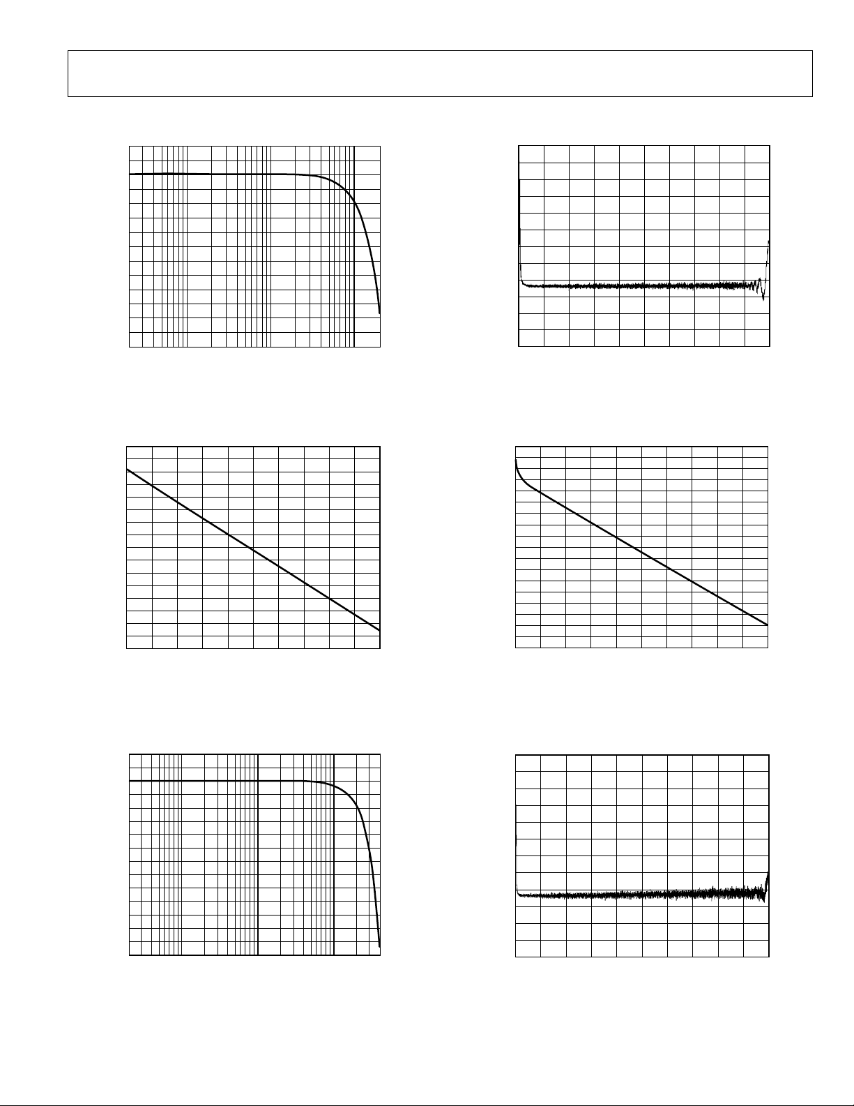
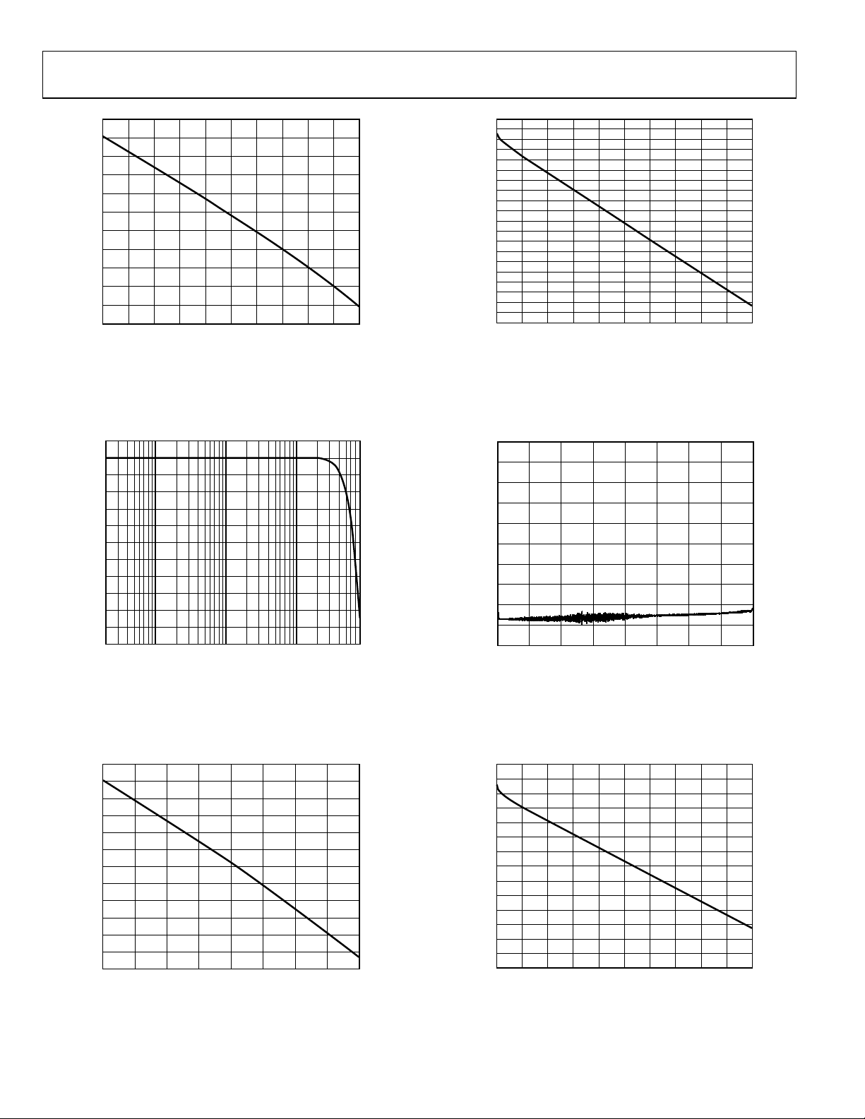
TYPICAL PERFORMANCE CHARACTERISTICS
= 48 kHz, Signal Path = AIN0 to DSP (Without Processing) to LOUTLx
f
S
Figure 11. Phase vs. Frequency, 20 kHz Bandwidth,
= 48 kHz, Signal Path = AIN0 to DSP (Without Processing) to LOUTLx
f
S
Figure 10. Relative Level vs. Frequency,
= 48 kHz, Signal Path = AIN0 to DSP (Without Processing) to LOUTLx
f
S
Figure 14. Phase vs. Frequency, 2 kHz Bandwidth,
= 48 kHz, Signal Path = AIN0 to DSP (Without Processing) to LOUTLx
f
S
Figure 13. Group Delay vs. Frequency,
= 96 kHz, Signal Path = AIN0 to DSP (Without Processing) to LOUTLx
f
S
Figure 12. Relative Level vs. Frequency,
= 96 kHz, Signal Path = AIN0 to DSP (Without Processing) to LOUTLx
f
S
Rev. 0 | Page 17 of 116
Figure 15. Group Delay vs. Frequency,
Page 18
ADAU1772 Data Sheet
50
–600
–550
–500
–450
–400
–350
–300
–250
–200
–150
–100
–50
0
0 4 8 12 16 20 24 28 32 36 40
PHASE (Degrees)
FREQUENCY ( kHz )
10804-015
1
–9
–8
–7
–6
–5
–4
–3
–2
–1
0
10k1k100
RELATIVE LEVEL (dB)
FREQUENCY ( Hz )
10804-016
200
–1300
–1200
–1100
–1000
–900
–800
–700
–600
–500
–400
–300
–200
–100
0
100
0 8070605040302010
PHASE (Degrees)
FREQUENCY ( kHz )
10804-017
6
–30
–28
–26
–24
–22
–20
–18
–16
–14
–12
–10
–8
–6
–4
–2
0
2
4
0 0.2 0.4 0.6 0.8 1.0 1.2 1.4 1.6 1.8 2.0
PHASE (Degrees)
FREQUENCY ( kHz )
10804-018
120
0
10
20
30
40
50
60
70
80
90
100
110
0 10 20 30 40 50 60 70 80
GROUP DEL AY ( µ s)
FREQUENCY ( kHz )
10804-019
6
–30
–28
–26
–24
–22
–20
–18
–16
–14
–12
–10
–8
–6
–4
–2
0
2
4
0 0.2 0.4 0.6 0.8 1.0 1.2 1.4 1.6 1.8 2.0
PHASE (Degrees)
FREQUENCY ( kHz )
10804-020
Figure 16. Phase vs. Frequency, 40 kHz Bandwidth,
= 96 kHz, Signal Path = AIN0 to DSP (Without Processing) to LOUTLx
f
S
Figure 17. Relative Level vs. Frequency,
= 192 kHz, Signal Path = AIN0 to DSP (Without Processing) to LOUTLx
f
S
Figure 19. Phase vs. Frequency, 2 kHz Bandwidth,
= 96 kHz, Signal Path = AIN0 to DSP (Without Processing) to LOUTLx
f
S
Figure 20. Group Delay vs. Frequency,
= 192 kHz, Signal Path = AIN0 to DSP (Without Processing) to LOUTLx
f
S
f
S
Figure 18. Phase vs. Frequency, 80 kHz Bandwidth,
= 192 kHz, Signal Path = AIN0 to DSP (Without Processing) to LOUTLx
= 192 kHz, Signal Path = AIN0 to DSP (Without Processing) to LOUTLx
f
S
Rev. 0 | Page 18 of 116
Figure 21. Phase vs. Frequency, 2 kHz Bandwidth,
Page 19
Data Sheet ADAU1772
0.04
–0.20
–0.18
–0.16
–0.14
–0.12
–0.10
–0.08
–0.06
–0.04
–0.02
0
0.02
100 1k 10k
RELATIVE LEVEL (dB)
FREQUENCY ( Hz )
10804-021
200
–1200
–1100
–1000
–900
–800
–700
–600
–500
–400
–300
–200
–100
0
100
0 2 4 6 8 10 12 14 16 18 20
PHASE (Degrees)
FREQUENCY ( kHz )
10804-022
0.4
–2.2
–2.0
–1.8
–1.6
–1.4
–1.2
–1.0
–0.8
–0.6
–0.4
–0.2
0
0.2
100 1k 10k
RELATIVE LEVEL (dB)
FREQUENCY ( Hz )
10804-023
300
280
260
240
220
200
180
160
140
120
100
80
60
40
20
0
0 2 4 6 8 10 12 14 16 18 20
GROUP DEL AY ( µ s)
FREQUENCY ( kHz )
10804-024
10
–100
–90
–80
–70
–60
–50
–40
–30
–20
–10
0
0 0.2 0.4 0.6 0.8 1.0 1.2 1.4 1.6 1.8 2.0
PHASE (Degrees)
FREQUENCY ( kHz )
10804-025
300
280
260
240
220
200
180
160
140
120
100
80
60
40
20
0
0 4 8 12 16 20 24 28 32 36 40
GROUP DEL AY ( µ s)
FREQUENCY ( kHz )
10804-026
Figure 22. Relative Level vs. Frequency,
= 48 kHz, Signal Path = AIN0 to ASRC to ADC_SDATA0
f
S
Figure 23. Phase vs. Frequency, 20 kHz Bandwidth,
= 48 kHz, Signal Path = AIN0 to ASRC to ADC_SDATA0
f
S
Figure 25. Group Delay vs. Frequency,
= 48 kHz, Signal Path = AIN0 to ASRC to ADC_SDATA0
f
S
Figure 26. Phase vs. Frequency, 2 kHz Bandwidth,
= 48 kHz, Signal Path = AIN0 to ASRC to ADC_SDATA0
f
S
Figure 24. Relative Level vs. Frequency,
= 96 kHz, Signal Path = AIN0 to ASRC to ADC_SDATA0
f
S
Figure 27. Group Delay vs. Frequency,
= 96 kHz, Signal Path = AIN0 to ASRC to ADC_SDATA0
f
S
Rev. 0 | Page 19 of 116
Page 20

ADAU1772 Data Sheet
200
–1500
–1400
–1300
–1200
–1100
–1000
–900
–800
–700
–600
–500
–400
–300
–200
–100
0
100
0 4 8 12 16 20 24 28 32 36 40
PHASE (Degrees)
FREQUENCY ( kHz )
10804-027
2
–22
–20
–18
–16
–14
–12
–10
–8
–6
–4
–2
0
10k100 1k
RELATIVE LEVEL (dB)
FREQUENCY ( Hz )
10804-028
200
–1800
–1600
–1400
–1200
–1000
–800
–600
–400
–200
0
800 10 20 30 40 50 60 70
PHASE (Degrees)
FREQUENCY ( kHz )
10804-029
10
–70
–65
–60
–55
–50
–45
–40
–35
–30
–25
–20
–15
–10
–5
0
5
0 0.2 0.4 0.6 0.8 1.0 1.2 1.4 1.6 1.8 2.0
PHASE (Degrees)
FREQUENCY ( kHz )
10804-030
300
0
20
40
60
80
100
120
140
160
180
220
260
280
200
240
0 10 20 30 40 50 60 70 80
GROUP DEL AY ( µ s)
FREQUENCY ( kHz )
10804-031
10
–40
–35
–30
–25
–20
–15
–10
–5
0
5
0 0.2 0.4 0.6 0.8 1.0 1.2 1.4 1.6 1.8 2.0
PHASE (Degrees)
FREQUENCY ( kHz )
10804-032
Figure 28. Phase vs. Frequency, 40 kHz Bandwidth,
= 96 kHz, Signal Path = AIN0 to ASRC to ADC_SDATA0
f
S
Figure 29. Relative Level vs. Frequency,
= 192 kHz, Signal Path = AIN0 to ASRC to ADC_SDATA0
f
S
Figure 31. Phase vs. Frequency, 2 kHz Bandwidth,
= 96 kHz, Signal Path = AIN0 to ASRC to ADC_SDATA0
f
S
Figure 32. Group Delay vs. Frequency,
= 192 kHz, Signal Path = AIN0 to ASRC to ADC_SDATA0
f
S
Figure 30. Phase vs. Frequency, 80 kHz Bandwidth,
= 192 kHz, Signal Path = AIN0 to ASRC to ADC_SDATA0
f
S
Figure 33. Phase vs. Frequency, 2 kHz Bandwidth,
= 192 kHz, Signal Path = AIN0 to ASRC to ADC_SDATA0
f
S
Rev. 0 | Page 20 of 116
Page 21

Data Sheet ADAU1772
0.02
–0.10
–0.09
–0.08
–0.07
–0.06
–0.05
–0.04
–0.03
–0.02
–0.01
0
0.01
100 1k 10k
RELATIVE LEVEL (dB)
FREQUENCY ( Hz )
10804-033
200
–1300
–1200
–1100
–1000
–900
–800
–700
–600
–500
–400
–300
–200
100
0
–100
PHASE (Degrees)
FREQUENCY ( kHz )
0 2 4 6 8 10 12 14 16 18 20
10804-034
0.2
–0.9
–0.8
–0.7
–0.6
–0.5
–0.4
–0.3
–0.2
–0.1
0
0.1
100 1k 10k
RELATIVE LEVEL (dB)
FREQUENCY ( Hz )
10804-035
300
0
20
40
60
80
100
120
140
160
180
200
220
240
260
280
GROUP DEL AY ( µ s)
FREQUENCY ( kHz )
0 2 4 6 8 10 12 14 16 18 20
10804-036
10
–120
–110
–100
–90
–80
–70
–60
–50
–40
–30
–20
0
–10
PHASE (Degrees)
FREQUENCY ( kHz )
0 0.2 0.4 0.6 0.8 1.0 1.2 1.4 1.6 1.8 2.0
10804-037
300
0
20
40
60
80
100
120
140
160
180
200
220
240
260
280
GROUP DEL AY ( µ s)
FREQUENCY ( kHz )
0 4 8 12 16 20 24 28 32 36 40
10804-038
Figure 34. Relative Level vs. Frequency,
= 48 kHz, Signal Path = DAC_SDATA to ASRC to LOUTLx
f
S
Figure 35. Phase vs. Frequency, 20 kHz Bandwidth,
= 48 kHz, Signal Path = DAC_SDATA to ASRC to LOUTLx
f
S
Figure 37. Group Delay vs. Frequency,
= 48 kHz, Signal Path = DAC_SDATA to ASRC to LOUTLx
f
S
Figure 38. Phase vs. Frequency, 2 kHz Bandwidth,
= 48 kHz, Signal Path = DAC_SDATA to ASRC to LOUTLx
f
S
Figure 36. Relative Level vs. Frequency,
= 96 kHz, Signal Path = DAC_SDATA to ASRC to LOUTLx
f
S
Figure 39. Group Delay vs. Frequency,
= 96 kHz, Signal Path = DAC_SDATA to ASRC to LOUTLx
f
S
Rev. 0 | Page 21 of 116
Page 22
ADAU1772 Data Sheet
200
–1700
–1600
–1500
–1400
–1300
–1200
–1100
–1000
–900
–800
–700
–600
–500
–400
–300
–200
–100
0
100
PHASE (Degrees)
FREQUENCY ( kHz )
0 4 8 12 16 20 24 28 32 36 40
10804-039
1.0
–8.0
–7.5
–7.0
–6.5
–6.0
–5.5
–5.0
–4.5
–4.0
–3.5
–3.0
–2.5
–2.0
–1.5
–1.0
–0.5
0
0.5
RELATIVE LEVEL (dB)
FREQUENCY ( Hz )
100 1k 10k
10804-040
200
–2800
–2600
–2400
–2200
–2000
–1800
–1600
–1400
–1200
–1000
–600
–200
0
–800
–400
0 10 20 30 40 50 60 70 80
PHASE (Degrees)
FREQUENCY ( kHz )
10804-041
10
–80
–75
–70
–65
–60
–55
–50
–45
–40
–35
–30
–25
–20
–15
–10
–5
0
5
PHASE (Degrees)
FREQUENCY ( kHz )
0 0.2 0.4 0.6 0.8 1.0 1.2 1.4 1.6 1.8 2.0
10804-042
300
0
20
40
60
80
100
120
140
160
180
200
220
240
260
280
800 10 20 30 40 50 60 70
GROUP DEL AY ( µ s)
FREQUENCY ( kHz )
10804-043
10
–60
–55
–50
–45
–40
–35
–30
–25
–20
–15
–10
–5
0
5
PHASE (Degrees)
FREQUENCY ( kHz )
0 0.2 0.4 0.6 0.8 1.0 1.2 1.4 1.6 1.8 2.0
10804-044
Figure 40. Phase vs. Frequency, 40 kHz Bandwidth,
= 96 kHz, Signal Path = DAC_SDATA to ASRC to LOUTLx
f
S
Figure 41. Relative Level vs. Frequency,
= 192 kHz, Signal Path = DAC_SDATA to ASRC to LOUTLx
f
S
Figure 43. Phase vs. Frequency, 2 kHz Bandwidth,
= 96 kHz, Signal Path = DAC_SDATA to ASRC to LOUTLx
f
S
Figure 44. Group Delay vs. Frequency,
= 192 kHz, Signal Path = DAC_SDATA to ASRC to LOUTLx
f
S
Figure 42. Phase vs. Frequency, 80 kHz Bandwidth,
= 192 kHz, Signal Path = DAC_SDATA to ASRC to LOUTLx
f
S
Figure 45. Phase vs. Frequency, 2 kHz Bandwidth,
= 192 kHz, Signal Path = DAC_SDATA to ASRC to LOUTLx
f
S
Rev. 0 | Page 22 of 116
Page 23
Data Sheet ADAU1772
0.020
–0.050
–0.045
–0.040
–0.035
–0.030
–0.025
–0.020
–0.015
–0.010
–0.005
0
0.005
0.010
0.015
100 1k 10k
RELATIVE LEVEL (dB)
FREQUENCY ( Hz )
10804-045
200
–1300
–1400
–1500
–1600
–1700
–1800
–1200
–1100
–1000
–900
–800
–700
–600
–500
–400
–300
–200
100
0
–100
PHASE (Degrees)
FREQUENCY ( kHz )
0 2 4 6 8 10 12 14 16 18 20
10804-046
0.4
–1.8
–1.6
–1.4
–1.2
–1.0
–0.8
–0.6
–0.4
–0.2
0
0.2
100 1k 10k
RELATIVE LEVEL (dB)
FREQUENCY ( Hz )
10804-047
500
0
50
100
150
200
250
300
350
400
450
GROUP DEL AY ( µ s)
FREQUENCY ( kHz )
0 2 4 6 8 10 12 14 16 18 20
10804-048
10
–160
–150
–140
–130
–120
–110
–100
–90
–80
–70
–60
–50
–40
–30
–20
–10
0
PHASE (Degrees)
FREQUENCY ( kHz )
0 0.2 0.4 0.6 0.8 1.0 1.2 1.4 1.6 1.8 2.0
10804-049
500
450
400
350
300
250
200
150
100
50
0
GROUP DEL AY ( µ s)
FREQUENCY ( kHz )
0 4 8 12 16 20 24 28 32 36 40
10804-050
= 48 kHz, Signal Path = DAC_SDATA to ASRC to DSP (Without Processing)
f
S
to ASRC to ADC_SDATA0
Figure 47. Phase vs. Frequency, 20 kHz Bandwidth,
Figure 46. Relative Level vs. Frequency,
= 48 kHz, Signal Path = DAC_SDATA to ASRC to DSP (Without Processing)
f
S
to ASRC to ADC_SDATA0
= 48 kHz, Signal Path = DAC_SDATA to ASRC to DSP (Without Processing)
f
S
to ASRC to ADC_SDATA0
Figure 50. Phase vs. Frequency, 2 kHz Bandwidth,
Figure 49. Group Delay vs. Frequency,
= 48 kHz, Signal Path = DAC_SDATA to ASRC to DSP (Without Processing)
f
S
to ASRC to ADC_SDATA0
= 96 kHz, Signal Path = DAC_SDATA to ASRC to DSP (Without Processing)
f
S
Figure 48. Relative Level vs. Frequency,
to ASRC to ADC_SDATA0
= 96 kHz, Signal Path = DAC_SDATA to ASRC to DSP (Without Processing)
f
S
to ASRC to ADC_SDATA0
Rev. 0 | Page 23 of 116
Figure 51. Group Delay vs. Frequency,
Page 24
ADAU1772 Data Sheet
200
–2000
–1800
–1600
–1400
–1200
–1000
–800
–600
–400
–200
0
PHASE (Degrees)
FREQUENCY ( kHz )
0 4 8 12 16 20 24 28 32 36 40
10804-051
2
–22
–20
–18
–16
–14
–12
–10
–8
–6
–4
–2
0
RELATIVE LEVEL (dB)
FREQUENCY ( Hz )
100 1k 10k
10804-052
200
–2200
–2000
–1800
–1600
–1400
–1200
–1000
–800
–600
–400
–200
0
800 10 20 30 40 50 60 70
PHASE (Degrees)
FREQUENCY ( kHz )
10804-053
10
–60
–65
–70
–75
–80
–85
–90
–55
–50
–45
–40
–35
–30
–25
–20
–15
–10
–5
0
5
PHASE (Degrees)
FREQUENCY ( kHz )
0 0.2 0.4 0.6 0.8 1.0 1.2 1.4 1.6 1.8 2.0
10804-054
500
0
50
100
150
200
250
300
350
400
450
800 10 20 30 40 50 60 70
GROUP DEL AY ( µ s)
FREQUENCY ( kHz )
10804-055
10
–60
–55
–50
–45
–40
–35
–30
–25
–20
–15
–10
–5
0
5
PHASE (Degrees)
FREQUENCY ( kHz )
0 0.2 0.4 0.6 0.8 1.0 1.2 1.4 1.6 1.8 2.0
10804-056
= 96 kHz, Signal Path = DAC_SDATA to ASRC to DSP (Without Processing)
f
S
to ASRC to ADC_SDATA0
Figure 53. Relative Level vs. Frequency,
Figure 52. Phase vs. Frequency, 40 kHz Bandwidth,
= 192 kHz, Signal Path = DAC_SDATA to ASRC to DSP (Without Processing)
f
S
to ASRC to ADC_SDATA0
= 96 kHz, Signal Path = DAC_SDATA to ASRC to DSP (Without Processing)
f
S
to ASRC to ADC_SDATA0
Figure 56. Group Delay vs. Frequency,
Figure 55. Phase vs. Frequency, 2 kHz Bandwidth,
= 192 kHz, Signal Path = DAC_SDATA to ASRC to DSP (Without Processing)
f
S
to ASRC to ADC_SDATA0
= 192 kHz, Signal Path = DAC_SDATA to ASRC to DSP (Without Processing)
f
S
Figure 54. Phase vs. Frequency, 80 kHz Bandwidth,
to ASRC to ADC_SDATA0
= 192 kHz, Signal Path = DAC_SDATA to ASRC to DSP (Without Processing)
f
S
to ASRC to ADC_SDATA0
Rev. 0 | Page 24 of 116
Figure 57. Phase vs. Frequency, 2 kHz Bandwidth,
Page 25
Data Sheet ADAU1772
35
30
25
20
15
10
5
0
INPUT IMPEDANCE (kΩ)
PGA GAIN SETTING (dB)
–12 –6 0 6 12 18 24 30 36
10804-057
2
–10
–8
–6
–4
–2
0
0 2015105
10804-100
MAGNITUDE ( dBFS)
FREQUENCY ( kHz )
–120
–100
–80
–60
–40
–20
0
0 100908070605040302010
10804-101
MAGNITUDE ( dBFS)
FREQUENCY ( kHz )
2
–10
–8
–6
–4
–2
0
0 2015105
10804-102
MAGNITUDE ( dBFS)
FREQUENCY ( kHz )
–120
–100
–80
–60
–40
–20
0
0 100908070605040302010
10804-103
MAGNITUDE ( dBFS)
FREQUENCY ( kHz )
2
–4
–3
–2
–1
0
1
0 2015105
10804-104
MAGNITUDE ( dBFS)
FREQUENCY ( kHz )
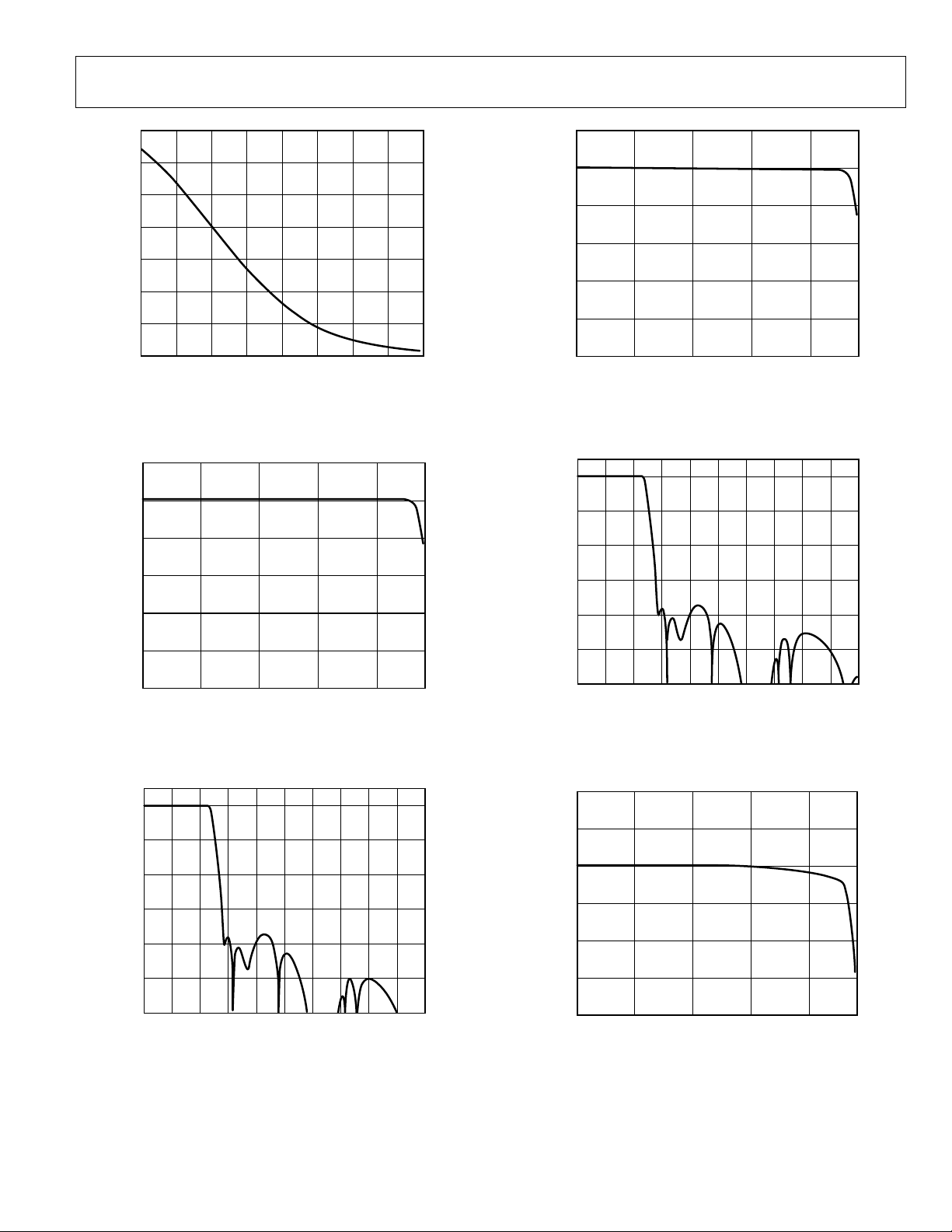
Figure 58. Input Impedance vs. PGA Gain
(see the Input Impedance section)
Figure 59. Decimation Pass-Band Response, fS = 96 kHz
Figure 61. Decimation Pass-Band Response, fS = 192 kHz
Figure 62. Total Decimation Response, f
= 192 kHz
S
Figure 60. Total Decimation Response, fS = 96 kHz
Figure 63. Interpolation Pass-Band Response, fS = 96 kHz
Rev. 0 | Page 25 of 116
Page 26
ADAU1772 Data Sheet
–120
–100
–80
–60
–40
–20
0
0 100908070605040302010
10804-105
MAGNITUDE ( dBFS)
FREQUENCY ( kHz )
2
–4
–3
–2
–1
0
1
MAGNITUDE ( dBFS)
FREQUENCY ( kHz )
0 2015105
10804-106
–120
–100
–80
–60
–40
–20
0
0 10987654321
10804-107
MAGNITUDE ( dBFS)
FREQUENCY ( kHz )
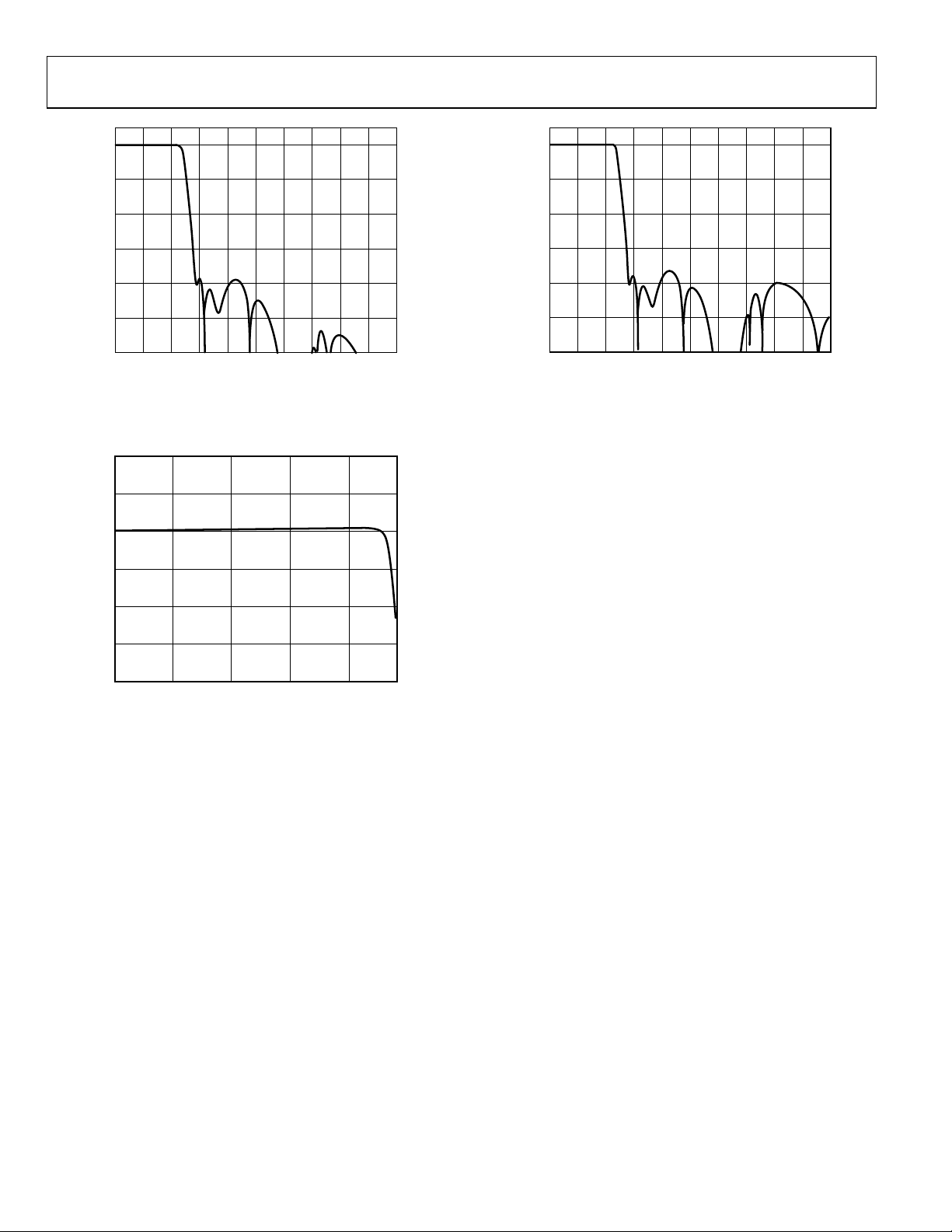
Figure 64. Total Interpolation Response, fS = 96 kHz
Figure 65. Interpolation Pass-Band Response, fS = 192 kHz
Figure 66. Total Interpolation Response, fS = 192 kHz
Rev. 0 | Page 26 of 116
Page 27
ADAU1772 Data Sheet
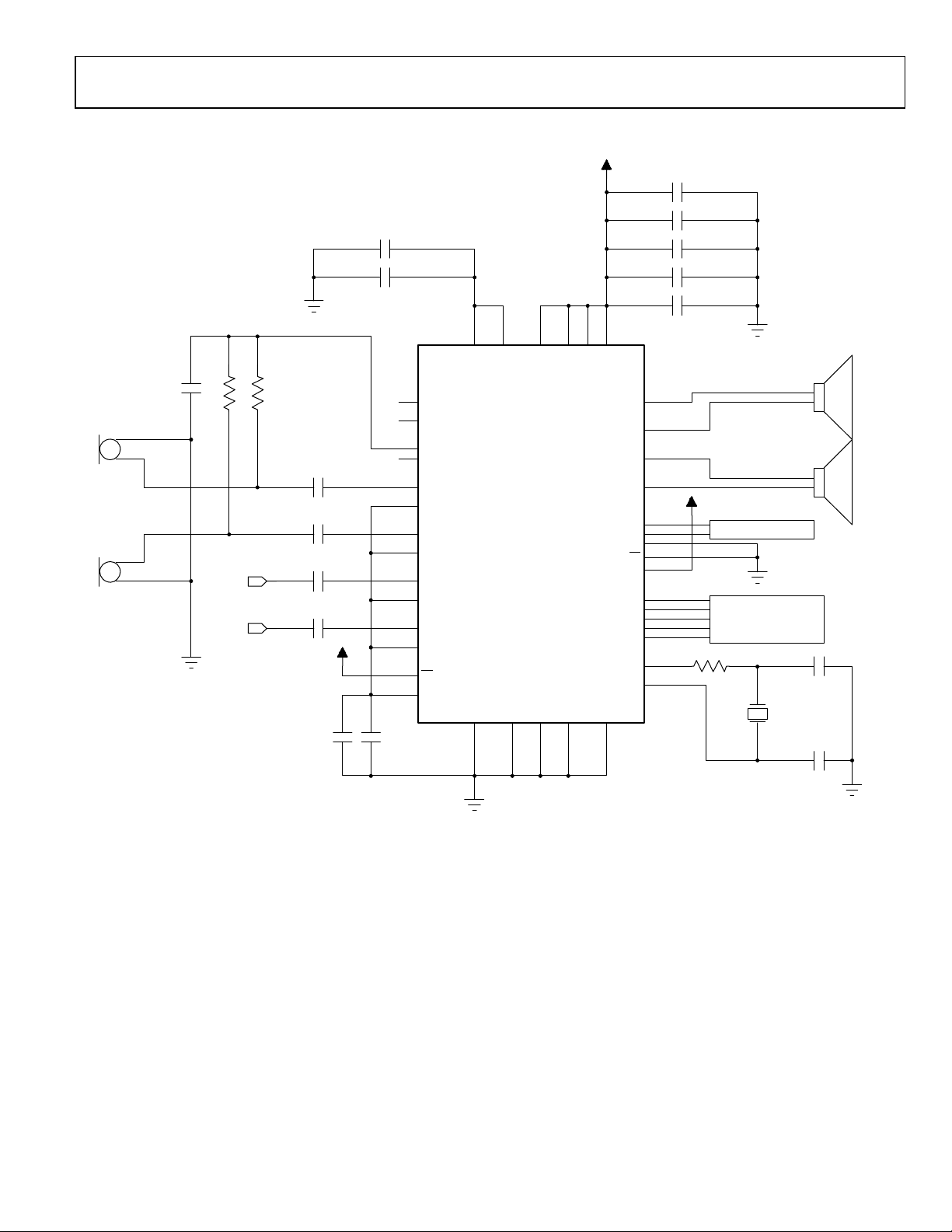
EEPROM
CONTROL INTERFACE:
SWITCHE S AND
POTENTIOMETERS
DC VOLTAGE SOURCE:
1.8 V TO 3.3 V
LEFT
MICROPHONE
RIGHT
MICROPHONE
LEFT HE ADP HONE
RIGHT HEADP HONE
1
SDA/MISO
2
SCL/SCLK
3
ADDR1/MOSI
4
ADDR0/SS
5
SELFBOOT
6
MICBIAS0
7
MICBIAS1
8
AIN0REF
9
AIN0
10
AVDD
11
13
AIN1REF
14
AIN1
15
AIN2REF
16
AIN2
12
CM
17
AIN3REF
18
AIN3
19
AVDD
20
23
AGND
AGND
AGND
DGND
24
AVDD
21
HPOUTLN/LOUTLN
22
HPOUTLP/LOUTLP
25
HPOUTRN/LOUTRN
26
HPOUTRP/LOUTRP
27
PD
40
IOVDD
28
REG_OUT
30
31
LRCLK/MP3
32
BCLK/MP2
33
DAC_SDATA/MP0
34
ADC_SDATA0/PDMOUT/MP1
38
XTALO
39
XTALI/MCLKIN
35
ADC_SDATA1/CLKOUT/MP6
36
DMIC2_3/MP5
37
DMIC0_1/MP4
29
DVDD
41
EP
ADAU1772
10µF
10µF
+
10µF
0.10µF
100Ω
22pF
22pF
+
10µF
0.10µF
+
10µF
0.10µF
0.10µF
0.10µF
0.10µF
47µF
47µF
2kΩ 2kΩ
1.0µF
LEFT_AUDIO
RIGHT_AUDIO
10804-060
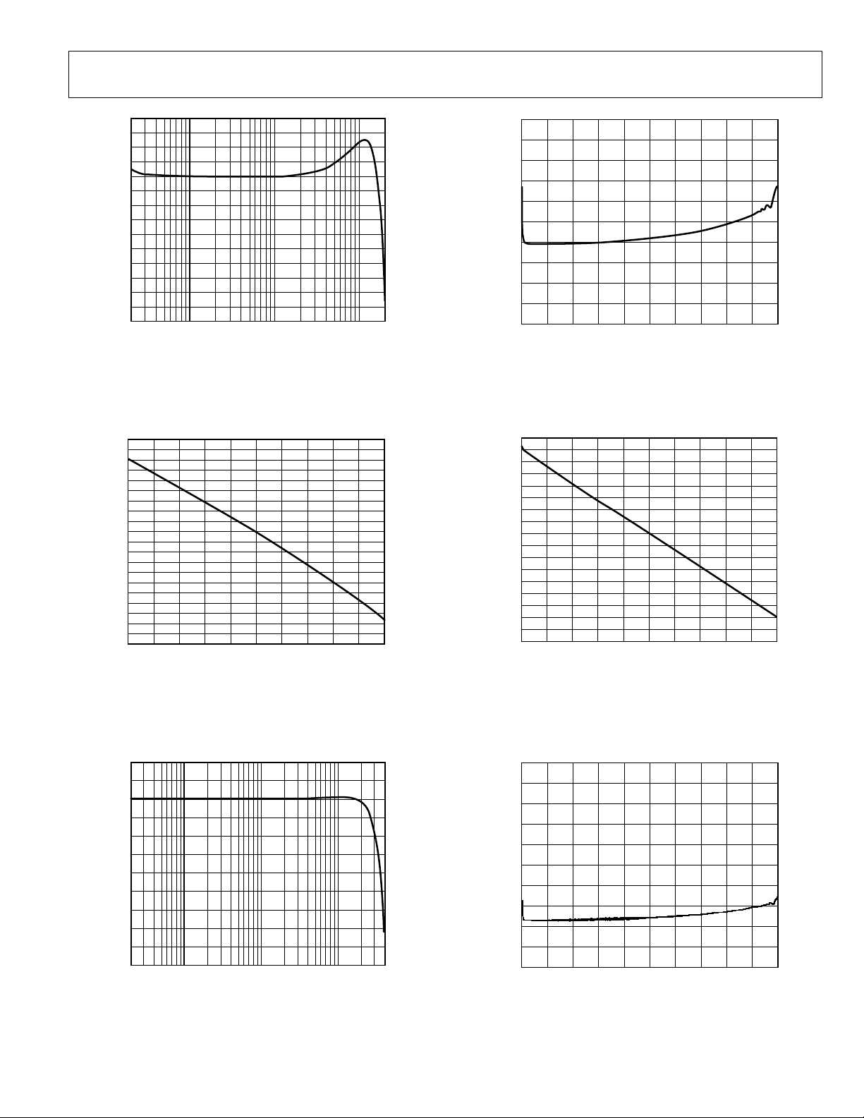
SYSTEM BLOCK DIAGRAMS
Figure 67. ADAU1772 System Block Diagram with Analog Microphones, Self-Boot Mode
Rev. 0 | Page 27 of 116
Page 28

ADAU1772 Data Sheet
THEORY OF OPERATION
The ADAU1772 is a low power audio codec with an optimized
audio processing core, making it ideal for noise cancelling
applications that require high quality audio, low power, small
size, and low latency. The four ADC and two DAC channels
each have an SNR of at least +96 dB and a THD + N of at least
−88 dB. The serial data port is compatible with I
right justified, and TDM modes, with tristating for interfacing
to digital audio data. The operating voltage range is 1.8 V to
3.63 V, w i t h a n o n-board regulator generating the internal
digital supply voltage. If desired, the regulator can be powered
down and the voltage can be supplied externally.
The input signal path includes flexible configurations that can
accept single-ended analog microphone inputs as well as up to
four digital microphone inputs. Two microphone bias pins provide
seamless interfacing to electret microphones. Each input signal
has its own programmable gain amplifier (PGA) for volume
adjustment.
The ADCs and DACs are high quality, 24-bit Σ-Δ converters
that operate at a selectable 192 kHz or 96 kHz sampling rate.
The ADCs have an optional high-pass filter with a cutoff
frequency of 1 Hz, 4 Hz, or 8 Hz. The ADCs and DACs also
include very fine-step digital volume controls.
The stereo DAC output is capable of differentially driving a
headphone earpiece speaker with 16 Ω impedance or higher.
One side of the differential output can be powered down if
single-ended operation is required. There is also the option to
change to line output mode when the output is lightly loaded.
The core has a reduced instruction set that optimizes this codec
for noise cancellation. The program and parameter RAMs can
be loaded with custom audio processing signal flow built using
the SigmaStudio™ graphical programming software from
Analog Devices, Inc. The values stored in the parameter RAM
2
S, left justified,
control individual signal processing blocks. The ADAU1772 also
has a self-boot function that can be used to load the program
and parameter RAM along with the register settings on powerup using an external EEPROM.
The SigmaStudio software is used to program and control the core
through the control port. Along with designing and tuning a signal
flow, the tools can be used to configure all of the ADAU1772
registers. The SigmaStudio graphical interface allows anyone with
digital or analog audio processing knowledge to easily design the
DSP signal flow and port it to a target application. The interface
also provides enough flexibility and programmability for an
experienced DSP programmer to have in-depth control of the
design. In SigmaStudio, the user can connect graphical blocks
(such as biquad filters, volume controls, and arithmetic operations),
compile the design, and load the program and parameter files into
the ADAU1772 memory through the control port. SigmaStudio
also allows the user to download the design to an external EEPROM
for self-boot operation. Signal processing blocks available in the
provided libraries include the following:
• Single-precision biquad filters
• Second order filters
• Absolute value and two-input adder
• Volume controls
• Limiter
The ADAU1772 can generate its internal clocks from a wide range
of input clocks by using the on-board fractional PLL. The PLL
accepts inputs from 8 MHz to 27 MHz. For standalone operation,
the clock can be generated using the on-board crystal oscillator.
The ADAU1772 is provided in a small, 40-lead, 6 mm × 6 mm
LFCSP with an exposed bottom pad.
Rev. 0 | Page 28 of 116
Page 29
Data Sheet ADAU1772
MCLK ÷X
× (R + N/M)
TO PLL
CLOCK DIVIDER
10804-061
SYSTEM CLOCKING AND POWER-UP
CLOCK INITIALIZATION
The ADAU1772 can generate its clocks either from an externally
provided clock or from a crystal oscillator. In both cases, the onboard PLL can be used or the clock can be fed directly to the
core. When a crystal oscillator is used, it is desirable to use a
12.288 MHz crystal, and the crystal oscillator function must be
enabled in the COREN bit (Address 0x0000). If the PLL is used,
it should always be set to output 24.576 MHz. The PLL can be
bypassed if a clock of 12.288 MHz or 24.576 MHz is available in
the system. Bypassing the PLL saves system power.
The CC_MDIV and CC_CDIV bits should not be changed after
setup, but the CLKSRC bit can be switched while the core is
running.
The CC_MDIV and CC_CDIV bits should be set so that the core
and internal master clock are always 12.288 MHz; for example,
when using a 24.576 MHz external source clock or if using the
PLL, it is necessary to use the internal divide by 2 (see Ta ble 11).
Table 11. Clock Configuration Settings
CC_MDIV CC_CDIV Description
1 1 Divide PLL/external clock by 1. Use these
settings for a 12.288 MHz direct input clock
source.
0 0 Divide PLL/external clock by 2. Use these
settings for a 24.576 MHz direct input clock
source or if using the PLL.
PLL Bypass Setup
On power up, the ADAU1772 comes out of an internal reset
after 12 ms. The rate of the internal master clock must be set
properly using the CC_MDIV bit in the clock control register
(Address 0x0000). When bypassing the PLL, the clock associated
with MCLKIN must be either 12.288 MHz or 24.576 MHz. The
internal master clock of the ADAU1772 is disabled until the
COREN bit is asserted.
PLL Enabled Setup
The core clock of the ADAU1772 is disabled by the default
setting of Bit COREN and should remain disabled during the
PLL lock acquisition period. The user can poll the LOCK bit to
determine when the PLL has locked. After lock is acquired, the
ADAU1772 can be started by asserting the COREN bit. This bit
enables the core clock for all the internal blocks of the ADAU1772.
To program the PLL during initialization or reconfiguration of
the codec, the following procedure must be followed:
1. Ensure that PLL_EN (Bit 7, Address 0x0000) is set low.
2. Set/reset the PLL control registers (Address 0x0001 to
Address 0x0005).
3. Enable the PLL using the PLL_EN bit.
4. Poll the PLL lock bit in Register 0x0006.
5. Set the COREN bit in Register 0x0000 after PLL lock is
acquired.
Control Port Access During Initialization
During the lock acquisition period, only Register 0x0000 to
Register 0x0006 are accessible through the control port. A read
or write to any other register is prohibited until the core clock
enable bit and the lock bit are both asserted.
After the CORE_RUN bit (Address 0x0009) is set high, the
DAC_SOURCE0 and DAC_SOURCE1 register bits should not
be changed. If these bits must be changed after the ADAU1772
is running, the CORE_RUN bit first must be disabled.
PLL
The PLL uses the MCLKIN signal as a reference to generate
the core clock. The PLL settings are set in Register 0x0000 to
Register 0x0005. Depending on the MCLK frequency, the PLL
must be set for either integer or fractional mode. The PLL can
accept input frequencies in the range of 8 MHz to 27 MHz.
Figure 68. PLL Block Diagram
Input Clock Divider
Before reaching the PLL, the input clock signal goes through an
integer clock divider to ensure that the clock frequency is within
a suitable range for the PLL. The X bits in the PLL_CTRL4 register
(Bits[2:1], Address 0x0005) sets the PLL input clock divide ratio.
Integer Mode
Integer mode is used when the clock input is an integer multiple
of the PLL output.
For example, if MCLKIN = 12.288 MHz and (X + 1) = 1, and
f
= 48 kHz, then
S
PLL Required Output = 24.576 MHz
R/2 = 24.576 MHz/12.288 MHz = 2
where R/2 = 2 or R = 4.
In integer mode, the values set for N and M are ignored.
Tabl e 12 lists common integer PLL parameter settings for
48 kHz sampling rates.
Fractional Mode
Fractional mode is used when the clock input is a fractional
multiple of the PLL output.
For example, if MCLKIN = 13 MHz, (X + 1) = 1, and
f
= 48 kHz, then
S
PLL Required Output = 24.576 MHz
(1/2) × (R + (N/M)) = 24.576 MHz/13 MHz = (1/2) × (3 +
(1269/1625))
where:
R = 3.
N = 1269.
M = 1625.
Rev. 0 | Page 29 of 116
Page 30
ADAU1772 Data Sheet
26 2 3
1625
1269
0x1B
0xF5
0x04
0x59
0x06
Tabl e 13 lists common fractional PLL parameter settings for
48 kHz sampling rates. When the PLL is used in fractional
mode, it is very important that the N/M fraction be kept in
the range of 0.1 to 0.9 to ensure correct operation of the PLL.
The PLL can output a clock in the range of 20.5 MHz to 27 MHz,
which should be taken into account when calculating PLL values
and MCLK frequencies.
CLOCK OUTPUT
The CLKOUT pin can be used as a master clock output to clock
other ICs in the system or as the clock for the digital microphone
inputs and PDM output. This clock can be generated from the
12.288 MHz master clock of the ADAU1772 by factors of 2, 1,
½, ¼, and ⅛. If PDM mode is enabled, only ½, ¼, and ⅛ settings
produce a clock signal on CLKOUT. The factor of 2 multiplier
works properly only if the input clock was previously divided by
2 using the CC_MDIV bit.
POWER SEQUENCING
AVDD and IOVDD can each be set to any voltage between 1.8 V
and 3.3 V, and DVDD can be set between 1.1 V and 1.8 V or
between 1.1 V and 1.2 V if using the on-board regulator.
On power-up, AVDD must be powered up before or at the same
time as IOVDD. IOVDD should not be powered up when power is
not applied to AVDD.
Enabling the
Before enabling
pin powers down all analog and digital circuits.
PD
(that is, setting it low), be sure to mute the
PD
outputs to avoid any pops when the IC is powered down.
can be tied directly to IOVDD for normal operation.
PD
Power-Down Considerations
When powering down the ADAU1772, be sure to mute the outputs
before AVDD power is removed; otherwise, pops or clicks may
be heard. The easiest way to achieve this is to use a regulator that
has a power good (PGOOD) signal to power the ADAU1772 or
generate a power good signal using additional circuitry external
to the regulator itself. Typically, on such regulators the power good
signal changes state when the regulated voltage drops below ~90%
of its target value. This power good signal can be connected to one
of the ADAU1772 multipurpose pins and used to mute the DAC
outputs by setting the multipurpose pin functionality to mute
both DACs in Register 0x0038 to Register 0x003E. This ensures
that the outputs are muted before power is completely removed.
Table 12. Integer PLL Parameter Settings for PLL Output = 24.576 MHz
Input Divider
MCLK Input (MHz)
12.288 1 4 Don’t care Don’t care 0x20
24.576 1 2 Don’t care Don’t care 0x10
(X + 1) Integer (R) Denominator (M) Numerator (N)
PLL_CTRL4 Settings
(Address 0x0005)
Table 13. Fractional PLL Parameter Settings for PLL Output = 24.576 MHz
PLL_CTRL[4:0] Settings
MCLK
Input
(MHz)
8 1 6 125 18 0x31 0x12 0x00 0x7D 0x00
13 1 3 1625 1269 0x19 0xF5 0x04 0x59 0x06
14.4 2 6 75 62 0x33 0x3E 0x00 0x4B 0x00
19.2 2 5 25 3 0x2B 0x03 0x00 0x19 0x00
27 2 3 1125 721 0x1B 0xD1 0x02 0x65 0x04
Input
Divider
(X + 1)
Integer
(R)
Denominator
(M)
Numerator
(N)
PLL_CTRL4
(0x0005)
(Address 0x0005 to Address 0x0001)
PLL_CTRL3
(0x0004)
PLL_CTRL2
(0x0003)
PLL_CTRL1
(0x0002)
PLL_CTRL0
(0x0001)
Rev. 0 | Page 30 of 116
Page 31

Data Sheet ADAU1772
ADC
MODULATOR
ADC
DECIMATOR
AIN0REF
AIN0
PGA
ADC
MODULATOR
ADC
DECIMATOR
AIN1REF
AIN1
PGA
ADC
MODULATOR
AIN2REF
AIN2
PGA
ADC
MODULATOR
AIN3REF
AIN3
DAC_SDATA
PGA
ADC
DECIMATOR
ADC
DECIMATOR
STEREO INPUT
ASRC
DMIC0_1/MP4
DMIC2_3/MP5
DIGITAL
MICROPHONE
INPUTS
HPOUTLN/LOUTLN
HPOUTLP/LOUTLP
DAC
HPOUTRN/LOUTRN
PDMOUT
1
ADC_SDATA0
1
ADC_SDATA1
HPOUTRP/LOUTRP
DAC
STEREO PDM
MODULATOR
CORE
INPUT
SELECTION
AUDIO
PROCESSING
CORE
DAC
AND
PDM
OUTPUT
SELECTION
SERIAL
INPUT PORT
SERIAL
OUTPUT PORT
1
THE ADC_SDATA0 AND PDMOUT FUNCTI ONS SHARE A PHYSICAL PIN, SO ONLY ONE O F THESE FUNCTIONS CAN BE USE D AT A TIME.
DUAL STEREO
OUTPUT ASRCs
10804-062
SIGNAL ROUTING
Figure 69. Input and Output Signal Routing
Rev. 0 | Page 31 of 116
Page 32

ADAU1772 Data Sheet
kΩ
110
40
)20/(
+
=
Gain
IN
R
MICROPHONE
PGA
–12dB TO
+35.25dB
ADAU1772
AINx
AINxREF
MICBIASx
CM
2kΩ
10804-063
ADAU1772
LINE INPUT 0 AIN0
LINE INPUT 1 AIN1
LINE INPUT 2 AIN2
LINE INPUT 3 AIN3
10804-064
INPUT SIGNAL PATHS
There are four input paths, from either an ADC or a digital
microphone, that can be routed to the core. The input sources
(ADC or digital microphone) must be configured in pairs (for
example, 0 and 1, 2 and 3), but each channel can be routed
individually. The core inputs can also be sourced from a stereo
input ASRC.
ANALOG INPUTS
The ADAU1772 can accept both line level and microphone inputs.
Each of the four analog input channels can be configured in a
single-ended mode or a single-ended with PGA mode. There
are also inputs for up to four digital microphones. The analog
inputs are biased at AVDD/2. Unused input pins should be
connected to the CM pin or ac-coupled to ground.
Signal Polarity
Signals routed through the PGAs are inverted. As a result, signals
input through the PGA are output from the ADCs with a polarity
that is opposite that of the input. Single-ended inputs are not
inverted. The ADCs are noninverting.
Input Impedance
The input impedance of the analog inputs varies with the gain of
the PGA. This impedance ranges from 0.68 kΩ at the 35.25 dB
gain setting to 32.0 kΩ at the −12 dB setting. The input impedance
on each pin can be calculated as follows:
where Gain is set by PGA_GAINx.
The optional 10 dB PGA boost set in PGA_x_BOOST does not
affect the input impedance. This is an alternative way of increasing
gain without decreasing input impedance; however, it causes some
degradation in performance.
Analog Microphone Inputs
For microphone signals, the ADAU1772 analog inputs can be
configured in single-ended with PGA mode.
The PGA settings are controlled in Register 0x0023 to Register
0x0026. The PGA is enabled by setting the PGA_ENx bits.
Connect the AINxREF pins to the CM pin and connect the
microphone signal to the inverting input of the PGAs (AINx),
as shown in Figure 70.
Analog Line Inputs
Line level signals can be input on the AINx pins of the analog
inputs. Figure 71 shows a single-ended line input using the
AINx pins. The AINxREF pins should be tied to CM. When using
single-ended line input, the PGA should be disabled using the
PGA_ENx bits, and the corresponding PGA pop suppression
bit should be disabled using the POP_SUPPRESS register
(Address 0x0029).
Figure 71. Single-Ended Line Inputs
Precharging Input Capacitors
Precharge amplifiers are enabled by default to quickly charge
large series capacitors on the inputs and outputs. Precharging
these capacitors helps to prevent pops in the audio signal. The
precharge circuits are powered up by default on startup and can be
disabled in the POP_SUPPRESS register. The precharge amplifiers
are automatically disabled when the PGA or headphone amplifiers
are enabled. For unused PGAs and headphone outputs, these
precharge amplifiers should be disabled using the POP_SUPPRESS
register. The precharging time is dependent on the input/output
series capacitors. The impedance looking into the pin is 500 Ω
in this mode. However, at startup, the impedance looking into
the pin is dominated by the time constant of the CM pin because
the precharge amplifiers reference the CM voltage.
Microphone Bias
The ADAU1772 includes two microphone bias outputs: MICBIAS0
and MICBIAS1. These pins provide a voltage reference for electret
analog microphones. The MICBIASx pins can also be used to
cleanly supply voltage to digital or analog MEMS microphones
with separate power supply pins. The MICBIASx voltage is set
in the microphone bias control register (Address 0x002D). Using
this register, either the MICBIAS0 or MICBIAS1 output can be
enabled and disabled. The gain options provide two possible
voltages: 0.65 × AVDD or 0.90 × AVDD.
Many applications require enabling only one of the two bias
outputs. The two bias outputs should both be enabled when many
microphones are used in the system or when the positioning of
the microphones on the PCB does not allow one pin to bias all
microphones.
Figure 70. Single-Ended Microphone Configuration
Rev. 0 | Page 32 of 116
Page 33

Data Sheet ADAU1772
ADAU1772
CLKOUT
DMIC0_1
ADMP421
CLK
V
DD
DATA
L/R SELECT GND
0.1µF
ADMP421
CLK
V
DD
DATA
L/R SELECT GND
0.1µF
1.8V TO 3.3V
10804-065
DIGITAL MICROPHONE INPUT
When using a digital microphone connected to the DMIC0_1/MP4
and DMIC2_3/MP5 pins, the DCM_0_1 and DCM_2_3 bits in
Register 0x001D and Register 0x001E must be set to enable the
digital microphone signal paths. The pin functions should also
be set to digital microphone input in the corresponding pin
mode registers (Address 0x003C and Address 0x003D). The
DMIC0/DMIC2 and DMIC1/DMIC3 channels can be swapped
(left/right swap) by writing to the DMIC_SW0 and DMIC_SW1
bits in the ADC_CONTROL2 and ADC_CONTROL3 registers
(Address 0x001D and Address 0x001E). In addition, the microphone polarity can be reversed by setting the DMIC_POLx bit,
which reverses the phase of the incoming audio by 180°.
The digital microphone inputs are clocked from the CLKOUT pin.
The digital microphone data stream must be clocked by this pin
and not by a clock from another source, such as another audio
IC, even if the other clock is of the same frequency as CLKOUT.
The digital microphone signal bypasses the analog input path
and the ADCs and is routed directly into the decimation filters.
The digital microphone and the ADCs share digital filters and,
therefore, both cannot be used simultaneously. The digital microphone inputs are enabled in pairs. The ADAU1772 inputs can be
set for either four analog inputs, four digital microphone inputs, or
two analog inputs and two digital microphone inputs. Figure 72
depicts the digital microphone interface and signal routing.
Figure 72 shows two ADMP421 digital microphones connected
to Pin DMIC0_1 of the ADAU1772. These microphones could
also be connected to DMIC2_3 if that signal path is to be used for
digital microphones. If more than two digital microphones are to
be used in a system, then up to two microphones would be connected to both DMIC0_ 1 and DMIC2_3 and the CLKOUT signal
would be fanned out to the clock input of all of the microphones.
ANALOG-TO-DIGITAL CONVERTERS
The ADAU1772 includes four 24-bit Σ-Δ analog-to-digital con-
verters (ADCs) with a selectable sample rate of 192 kHz or 96 kHz.
ADC Full-Scale Level
The full-scale input to the ADCs (0 dBFS) scales linearly with
AVDD. At AVDD = 3.3 V, the full-scale input level is 1 V rms.
Signal levels above the full-scale value cause the ADCs to clip.
Digital ADC Volume Control
The volume setting of each ADC can be digitally attenuated in the
ADCx_VOLUME registers (Address 0x001F to Address 0x0022).
The volume can be set between 0 dB and −95.625 dB in 0.375 dB
steps. The ADC volume can also be digitally muted in the
ADC_CONTROLx registers (Address 0x001B to Address 0x001E).
High-Pass Filter
A high-pass filter is available on the ADC path to remove dc offsets;
this filter can be enabled or disabled using the HP_x_x_EN bits.
At f
= 192 kHz, the corner frequency of this high-pass filter can
S
be set to 1 Hz, 4 Hz, or 8 Hz.
Figure 72. Digital Microphone Interface Block Diagram
Rev. 0 | Page 33 of 116
Page 34

ADAU1772 Data Sheet
HP_EN_X
1 = HEADPHONE
HP_MUTE_R AND HP_MUTE_L
00 = UNMUTE
INTERNAL
PRECHARGE
6ms
USER
DEFINED
10804-066
OUTPUT SIGNAL PATHS
Data from the serial input port can be routed to the core either
directly or through a sample rate converter. Data can be routed
to the serial output port, the stereo DAC, and the stereo PDM
modulator.
The analog outputs of the ADAU1772 can be configured as
differential or single-ended outputs. The analog output pins are
capable of driving headphone or earpiece speakers. The line
outputs can drive a load of at least 10 kΩ or can be put into
headphone mode to drive headphones or earpiece speakers. The
analog output pins are biased at AVDD/2.
ANALOG OUTPUTS
Headphone Output
The output pins can be driven by either a line output driver or a
headphone driver by setting the HP_EN_L and HP_EN_R bits
in the headphone line output select register (Address 0x0043).
The headphone outputs can drive a load of at least 16 Ω.
Headphone Output Power-Up Sequencing
To prevent pops when turning on the headphone outputs, the
user must wait at least 6 ms to unmute these outputs after enabling
the headphone output using the HP_EN_x bits. Waiting 6 ms
allows an internal capacitor to charge before these outputs are
used. Figure 73 illustrates the headphone output power-up
sequencing.
Pop-and-Click Suppression
On power-up, the precharge circuitry is enabled on all four
analog output pins to suppress pops and clicks. After powerup, the precharge circuitry can be put into a low power mode
using the HP_POP_DISx bits in the POP_SUPRRESS register
(Address 0x0029).
The precharge time depends on the value of the capacitor
connected to the CM pin and the RC time constant of the load
on the output pin. For a typical line output load, the precharge
time is between 2 ms and 3 ms. After this precharge time, the
HP_POP_DISx bit can be set to low power mode.
To avoid clicks and pops, all analog outputs that are in use should
be muted while changing any register settings that may affect the
signal path. These outputs can then be unmuted after the changes
have been made.
Line Outputs
The analog output pins (HPOUTLP/LOUTLP, HPOUTLN/
LOUTLN, HPOUTRP/LOUTRP, and HPOUTRN/LOUTRN)
can be used to drive both differential and single-ended loads. In
their default settings, these pins can drive typical line loads of
10 kΩ or greater.
When the line output pins are used in single-ended mode, the
HPOUTLP/LOUTLP and HPOUTRP/LOUTRP pins should be
used to output the signals, and the HPOUTLN/LOUTLN and
HPOUTRN/LOUTRN pins should be powered down.
Figure 73. Headphone Output Power-Up Timing
Ground-Centered Headphone Configuration
The headphone outputs can also be configured as groundcentered outputs by connecting coupling capacitors in series
with the output pins. Ground-centered headphones should use
the AGND pin as the ground reference.
When the headphone outputs are configured in this manner,
the capacitors create a high-pass filter on the outputs. The
corner frequency of this filter, which has an attenuation of 3 dB
at this point, is calculated by the following formula:
f
= 1/(2π × R × C)
3dB
where :
R is the impedance of the headphones.
C is the capacitor value.
For a typical headphone impedance of 32 Ω and a 220 μF
capacitor, the corner frequency is 23 Hz.
DIGITAL-TO-ANALOG CONVERTERS
The ADAU1772 includes two 24-bit Σ-Δ digital-to-analog
converters (DACs).
DAC Full-Scale Level
The full-scale output from the DACs (0 dBFS) scales linearly
with AVDD. At AVDD = 3.3 V, the full-scale output level is
1.94 V rms for a differential output or 0.97 V rms for a singleended output.
Digital DAC Volume Control
The volume of each DAC can be digitally attenuated using the
DACx_VOLUME registers (Address 0x002F and Address 0x0030).
The volume can be set to be between 0 dB and −95.625 dB in
0.375 dB steps.
PDM OUTPUT
The ADAU1772 includes a 2-channel pulse density modulated
(PDM) modulator. The PDMOUT pin can be used to drive a
PDM input amplifier, such as the SSM2517 mono 2.4 W
amplifier. Two SSM2517 devices can be connected to the
PDMOUT data stream to enable a stereo output. The PDM
output signal is clocked by the CLKOUT pin output. The PDM
output stream must be clocked by this pin and not by a clock
from another source, such as another audio IC, even if the other
clock is of the same frequency as CLKOUT. The PDM output
Rev. 0 | Page 34 of 116
Page 35

Data Sheet ADAU1772
0xD1
f
set to opposite value determined by GAIN_FS pin.
ADC
INPUT
ASRCS
–2.5dB
DAC
+2.5dB
–2.5dB
OUTPUT
ASRCS
+2.5dB
CORE
10804-067
data is clipped at the −6 dB level to prevent overdriving a
connected amplifier like the SSM2517.
The ADAU1772 has the ability to output PDM control patterns to
configure devices such as the SSM2517. Each pattern is a byte long
and is written with a user defined pattern in the PDM_PATTERN
register (Address 0x0037). The control pattern is enabled and
the output channel selection is configured in the PDM_OUT
register (Address 0x0036). The PDM pattern should not be
changed while the ADAU1772 is outputting the control pattern
to the external device. After the external device is configured,
the control pattern can be disabled. For the SSM2517, the
control pattern must be repeated a minimum of 128 times to
configure the part. Tab l e 14 describes typical control patterns
for the SSM2517.
Table 14. SSM2517 PDM Control Pattern Descriptions
Pattern Control Description
0xAC
0xD8
0xD4
0xD2
0xE1
0xE2
0xE4
Power-down. All blocks off except for the PDM
interface. Normal start-up time.
Gain optimized for PVDD = 5 V operation. Overrides
GAIN_FS pin setting.
Gain optimized for PVDD = 3.6 V operation. Overrides
GAIN_FS pin setting.
Gain optimized for PVDD = 2.5 V operation. Overrides
GAIN_FS pin setting.
S
Ultralow EMI mode.
Half clock cycle pulse mode for power savings.
Special 32 kHz/128 × fS operation mode.
ASYNCHRONOUS SAMPLE RATE CONVERTERS
The ADAU1772 includes asynchronous sample rate converters
(ASRCs) to enable synchronous full-duplex operation of the
serial ports. Two stereo ASRCs are available for the digital outputs,
and one stereo ASRC is available for the digital input signals.
The ASRCs can convert serial output data from the core rate of
up to 192 kHz back down to less than 8 kHz. All intermediate
frequencies and ratios are also supported.
SIGNAL LEVELS
The ADCs, DACs, and ASRCs have fixed gain settings that should
be considered when configuring the system. These settings were
chosen to maximize performance of the converters and to ensure
that there is 0 dB gain for any signal path from the input of the
ADAU1772 to its output. Therefore, the full-scale level of a signal
in the processing core will be slightly different from a full-scale
level external to the IC.
Input paths, such as through the ADCs and input ASRCs, are
scaled by 0.75, or about −2.5 dB. Output paths, such as through
the DACs or output ASRCs, are scaled by 1.33, or about 2.5 dB.
This is shown in Figure 74.
Figure 74. Signal Level Diagram
Because of this input and output scaling, output signals from
the core should be limited to −2.5 dB full scale to prevent the
DACs and ASRCs from clipping.
Rev. 0 | Page 35 of 116
Page 36

ADAU1772 Data Sheet
Filter Coefficient (B0, B1, B2)
5.27
3
0x0083
14
0x008E
20
0x0094
25
0x0099
31
0x009F
SIGNAL PROCESSING
The ADAU1772 processing core is optimized for active noise
cancelling (ANC) processing. The processing capabilities of the
core include biquad filters, limiters, volume controls, and mixing.
The core has four inputs and four outputs. The core is controlled
with a 10-bit program word, with a maximum of 32 instructions
per frame.
INSTRUCTIONS
A complete list of instructions/processing blocks along with
documentation can be found in the SigmaStudio software for
the ADAU1772. The processing blocks available are
• Single-precision biquad/second order filters
• Absolute value
• Two -input addition
• T connection in SigmaStudio
• Limiter with/without external detector loop
• Linear gain
• Volume slider
• Mute
• DBREG level detection
DATA MEMORY
The ADAU1772 data path is 26 bits (5.21 format). The data
memory is 32 words of 2 × 26 bits. The double length memory
enables the core to double precision arithmetic with double
length data and single length coefficients.
PARAMETERS
Parameters, such as filter coefficients, limiter settings, and volume
control settings, are saved in parameter registers. Each parameter is
a 32-bit number. The format of this number depends on whether it
is controlling a filter or a limiter. The number formats of different
parameters are shown in Ta ble 15. When the parameter formats
use less than the full 32-bit memory space, as with the limiter
parameters, the data is LSB-aligned.
Table 15. Parameter Number Formats
Parameter Type Format
Filter Coefficient (A1) 2.27 (sign extended)
Filter Coefficient (A2) 1.27 (sign extended)
Maximum Gain 2.23
Minimum Gain 2.23
Attack Time 24.0
Decay Time 24.0
Threshold 2.23
There are two parameter banks available. Each bank can hold a
full set of 160 parameters (32 filters × 5 coefficients). Users can
switch between Bank A and Bank B, allowing for two sets of
parameters to be saved in memory and switched on the fly
while the codec is running. Bank switching can be achieved by
writing to the CORE_CONTROL register (Address 0x0009) or
by using the multipurpose push-button switches, but not using
a combination of the two. Parameters in the active bank should
not be updated while the core is running; this will likely result
in noises on the outputs.
Parameters are assigned to instructions in the order in which
the instructions are instantiated in the code. The instruction
types that use parameters are the biquad filters and limiters.
Tabl e 17 shows the addresses of each parameter in Bank A that
are associated with each of the 32 instructions, and Ta b le 18 shows
the addresses of each parameter in Bank B. Ta b l e 16 shows the
addresses of the LSB aligned, 10-bit program words.
Table 16. Program Addresses
Instruction Instruction Address
0 0x0080
1 0x0081
2 0x0082
4 0x0084
5 0x0085
6 0x0086
7 0x0087
8 0x0088
9 0x0089
10 0x008A
11 0x008B
12 0x008C
13 0x008D
15 0x008F
16 0x0090
17 0x0091
18 0x0092
19 0x0093
21 0x0095
22 0x0096
23 0x0097
24 0x0098
26 0x009A
27 0x009B
28 0x009C
29 0x009D
30 0x009E
Rev. 0 | Page 36 of 116
Page 37

Data Sheet ADAU1772
1
0x00E1
0x0101
0x0121
0x0141
0x0161
6
0x00E6
0x0106
0x0126
0x0146
0x0166
12
0x00EC
0x010C
0x012C
0x014C
0x016C
18
0x00F2
0x0112
0x0132
0x0152
0x0172
23
0x00F7
0x0117
0x0137
0x0157
0x0177
29
0x00FD
0x011D
0x013D
0x015D
0x017D
2
0x0182
0x01A2
0x01C2
0x01E2
0x0202
13
0x018D
0x01AD
0x01CD
0x01ED
0x020D
Table 17. Parameter Addresses, Bank A
Assignment Order B0/Max Gain B1/Min Gain B2/Attack A1/Decay A2/Threshold
0 0x00E0 0x0100 0x0120 0x0140 0x0160
2 0x00E2 0x0102 0x0122 0x0142 0x0162
3 0x00E3 0x0103 0x0123 0x0143 0x0163
4 0x00E4 0x0104 0x0124 0x0144 0x0164
5 0x00E5 0x0105 0x0125 0x0145 0x0165
7 0x00E7 0x0107 0x0127 0x0147 0x0167
8 0x00E8 0x0108 0x0128 0x0148 0x0168
9 0x00E9 0x0109 0x0129 0x0149 0x0169
10 0x00EA 0x010A 0x012A 0x014A 0x016A
11 0x00EB 0x010B 0x012B 0x014B 0x016B
13 0x00ED 0x010D 0x012D 0x014D 0x016D
14 0x00EE 0x010E 0x012E 0x014E 0x016E
15 0x00EF 0x010F 0x012F 0x014F 0x016F
16 0x00F0 0x0110 0x0130 0x0150 0x0170
17 0x00F1 0x0111 0x0131 0x0151 0x0171
19 0x00F3 0x0113 0x0133 0x0153 0x0173
20 0x00F4 0x0114 0x0134 0x0154 0x0174
21 0x00F5 0x0115 0x0135 0x0155 0x0175
22 0x00F6 0x0116 0x0136 0x0156 0x0176
24 0x00F8 0x0118 0x0138 0x0158 0x0178
25 0x00F9 0x0119 0x0139 0x0159 0x0179
26 0x00FA 0x011A 0x013A 0x015A 0x017A
27 0x00FB 0x011B 0x013B 0x015B 0x017B
28 0x00FC 0x011C 0x013C 0x015C 0x017C
30 0x00FE 0x011E 0x013E 0x015E 0x017E
31 0x00FF 0x011F 0x013F 0x015F 0x017F
Table 18. Parameter Addresses, Bank B
Assignment Order B0/Max Gain B1/Min Gain B2/Attack A1/Decay A2/Threshold
0 0x0180 0x01A0 0x01C0 0x01E0 0x0200
1 0x0181 0x01A1 0x01C1 0x01E1 0x0201
3 0x0183 0x01A3 0x01C3 0x01E3 0x0203
4 0x0184 0x01A4 0x01C4 0x01E4 0x0204
5 0x0185 0x01A5 0x01C5 0x01E5 0x0205
6 0x0186 0x01A6 0x01C6 0x01E6 0x0206
7 0x0187 0x01A7 0x01C7 0x01E7 0x0207
8 0x0188 0x01A8 0x01C8 0x01E8 0x0208
9 0x0189 0x01A9 0x01C9 0x01E9 0x0209
10 0x018A 0x01AA 0x01CA 0x01EA 0x020A
11 0x018B 0x01AB 0x01CB 0x01EB 0x020B
12 0x018C 0x01AC 0x01CC 0x01EC 0x020C
14 0x018E 0x01AE 0x01CE 0x01EE 0x020E
15 0x018F 0x01AF 0x01CF 0x01EF 0x020F
16 0x0190 0x01B0 0x01D0 0x01F0 0x0210
Rev. 0 | Page 37 of 116
Page 38

ADAU1772 Data Sheet
21
0x0195
0x01B5
0x01D5
0x01F5
0x0215
27
0x019B
0x01BB
0x01DB
0x01FB
0x021B
Assignment Order B0/Max Gain B1/Min Gain B2/Attack A1/Decay A2/Threshold
17 0x0191 0x01B1 0x01D1 0x01F1 0x0211
18 0x0192 0x01B2 0x01D2 0x01F2 0x0212
19 0x0193 0x01B3 0x01D3 0x01F3 0x0213
20 0x0194 0x01B4 0x01D4 0x01F4 0x0214
22 0x0196 0x01B6 0x01D6 0x01F6 0x0216
23 0x0197 0x01B7 0x01D7 0x01F7 0x0217
24 0x0198 0x01B8 0x01D8 0x01F8 0x0218
25 0x0199 0x01B9 0x01D9 0x01F9 0x0219
26 0x019A 0x01BA 0x01DA 0x01FA 0x021A
28 0x019C 0x01BC 0x01DC 0x01FC 0x021C
29 0x019D 0x01BD 0x01DD 0x01FD 0x021D
30 0x019E 0x01BE 0x01DE 0x01FE 0x021E
31 0x019F 0x01BF 0x01DF 0x01FF 0x021F
Rev. 0 | Page 38 of 116
Page 39

Data Sheet ADAU1772
ADDR1/MOSI
I2C Address Bit 1—input
MOSI—input
0 0 0x3C
CONTROL PORT
The ADAU1772 has both a 4-wire SPI control port and a 2-wire
2
C bus control port. Each can be used to set the memories and
I
registers. The IC defaults to I
control mode by pulling the
2
C mode but can be put into SPI
SS
pin low three times.
The control port is capable of full read/write operation for all
addressable memories and registers. Most signal processing
parameters are controlled by writing new values to the parameter memories using the control port. Other functions, such as
mute and input/output mode control, are programmed through
the registers.
All addresses can be accessed in either single-address mode or
burst mode. The first byte (Byte 0) of a control port write contains
the 7-bit IC address plus the R/
bit. The next two bytes (Byte 1
W
and Byte 2) are the 16-bit subaddress of the memory or register
location within the ADAU1772. All subsequent bytes (starting
with Byte 3) contain the data, such as register data, program
data, or parameter data. The number of bytes per word depends
on the type of data that is being written. Ta ble 19 shows the word
length of the ADAU1772’s different data types. The exact formats
for specific types of writes are shown in Figure 77 and Figure 78.
Table 19. Data Word Sizes
Data Type Word Size (bytes)
Registers 1
Program 2
Parameters 4
If large blocks of data need to be downloaded to the ADAU1772,
the output of the core can be halted (using the CORE_RUN bit
in the core control register (Address 0x0009)), new data can be
loaded, and then the core can be restarted. This is typically done
during the booting sequence at start-up or when loading a new
program into memory.
Registers and bits shown as reserved in the register map read back
0s. When writing to these registers and bits, such as during a burst
write across a reserved register, or when writing to reserved bits
in a register with other used bits, write 0s.
The control port pins are multifunctional, depending on the
mode in which the part is operating. Ta bl e 20 details these
multiple functions.
Table 20. Control Port Pin Functions
Pin I2C Mode SPI Mode
SCL/SCLK SCL—input SCLK—input
SDA/MISO SDA—open-collector output MISO—output
2
I
ADDR0/SS
C Address Bit 0—input
SS—input
Burst Mode Communication
Burst mode addressing, in which the subaddresses are automatically incremented at word boundaries, can be used for writing
Rev. 0 | Page 39 of 116
large amounts of data to contiguous memory locations. This
increment happens automatically after a single-word write unless
the control port communication is stopped (that is, a stop
condition is issued for I
2
C, or SS is brought high for SPI). The
registers and RAMs in the ADAU1772 range in width from one
to four bytes, so the auto-increment feature knows the mapping
between subaddresses and the word length of the destination
register (or memory location).
I2C PORT
The ADAU1772 supports a 2-wire serial (I2C-compatible)
microprocessor bus driving multiple peripherals. I
pins—serial data (SDA) and serial clock (SCL)—to carry data
between the ADAU1772 and the system I
2
In I
C mode, the ADAU1772 is always a slave on the bus, except
2
C master controller.
when the IC is self-booting. See the Self-Boot section for details
about using the ADAU1772 in self-boot mode.
Each slave device is recognized by a unique 7-bit address. The
ADAU1772 I
this first byte sent from the I
2
C address format is shown in Tabl e 21. The LSB of
2
C master sets either a read or write
operation. Logic Level 1 corresponds to a read operation, and
Logic Level 0 corresponds to a write operation.
Pin ADDR0 and Pin ADDR1 set the LSBs of the I
(Tabl e 22); therefore, each ADAU1772 can be set to one of four
unique addresses. This allows multiple ICs to exist on the same
2
I
C bus without address contention. The 7-bit I2C addresses are
shown in Tabl e 22.
2
An I
C data transfer is always terminated by a stop condition.
Both SDA and SCL should have 2.0 kΩ pull-up resistors on the
lines connected to them. The voltage on these signal lines should
not be higher than IOVDD.
2
Table 21. I
Bit 6 Bit 5 Bit 4 Bit 3 Bit 2 Bit 1 Bit 0
0 1 1 1 1 ADDR1 ADDR0
C Address Format
Table 22. I2C Addresses
ADDR1 ADDR0 Slave Address
0 1 0x3D
1 0 0x3E
1 1 0x3F
Addressing
Initially, each device on the I2C bus is in an idle state and
monitoring the SDA and SCL lines for a start condition and
the proper address. The I
2
C master initiates a data transfer by
establishing a start condition, defined by a high-to-low transition
on SDA while SCL remains high. This indicates that an address/
data stream follows. All devices on the bus respond to the start
condition and shift the next eight bits (the 7-bit address plus the
2
C uses two
2
C address
Page 40

ADAU1772 Data Sheet
R/W
0
SCL
SDA
SDA
(CONTINUED)
SCL
(CONTINUED)
1 1 1
ADDR0ADDR1
1
START BY
MASTER
FRAME 1
CHIP ADDRESS BYTE
FRAME 2
SUBADDRESS BYTE 1
FRAME 3
SUBADDRESS BYTE 2
FRAME 4
DATA BYTE 1
ACKNOWLEDGE
BY ADAU1772
ACKNOWLEDGE
BY ADAU1772
ACKNOWLEDGE
BY ADAU1772
ACKNOWLEDGE
BY ADAU1772
STOP BY
MASTER
10804-068
R/W
SCL
SDA
SDA
(CONTINUED)
SCL
(CONTINUED)
SDA
(CONTINUED)
SCL
(CONTINUED)
START BY
MASTER
FRAME 2
SUBADDRESS BYTE 1
FRAME 3
SUBADDRESS BYTE 2
FRAME 4
CHIP ADDRESS BYTE
FRAME 1
CHIP ADDRESS BYTE
FRAME 5
READ DATA BYTE 1
FRAME 6
READ DATA BYTE 2
ACKNOWLEDGE
BY ADAU1772
ACKNOWLEDGE
BY ADAU1772
ACKNOWLEDGE
BY ADAU1772
ACKNOWLEDGE
BY ADAU1772
ACKNOWLEDGE
BY ADAU1772
STOP BY
MASTER
ACKNOWLEDGE
BY ADAU1772
REPEATED
START BY MASTER
R/W
ADDR0
ADDR0ADDR1
ADDR1
0 1 1 1
1
0 1 1 1
1
10804-069
R/W bit) MSB first. The device that recognizes the transmitted
address responds by pulling the data line low during the ninth
clock pulse. This ninth bit is known as an acknowledge bit. All
other devices withdraw from the bus at this point and return to
the idle condition. The R/
bit determines the direction of the
W
data. A Logic 0 on the LSB of the first byte indicates that the master
will write information to the peripheral, whereas a Logic 1 indicates
that the master will read information from the peripheral after
writing the subaddress and repeating the start address. A data
transfer takes place until a stop condition is encountered. A stop
condition occurs when SDA transitions from low to high while
SCL is held high.
and Figure 76 shows an I
Figure 75 shows the timing of an I2C write,
2
C read.
Stop and start conditions can be detected at any stage during the
data transfer. If these conditions are asserted out of sequence with
normal read and write operations, the ADAU1772 immediately
jumps to the idle condition. During a given SCL high period,
the user should only issue one start condition, one stop condition,
or a single stop condition followed by a single start condition. If
an invalid subaddress is issued by the user, the ADAU1772 does
not issue an acknowledge and returns to the idle condition. If
the user exceeds the highest subaddress while in auto-increment
mode, one of two actions is taken. In read mode, the ADAU1772
outputs the highest subaddress register contents until the master
device issues a no acknowledge, indicating the end of a read. A
no-acknowledge condition is where the SDA line is not pulled
low on the ninth clock pulse on SCL. If the highest subaddress
location is reached while in write mode, the data for the invalid
byte is not loaded into any subaddress register, a no acknowledge
is issued by the ADAU1772, and the part returns to the idle
condition.
Figure 75. I
Figure 76. I
2
C Write to ADAU1772 Clocking
2
C Read from ADAU1772 Clocking
Rev. 0 | Page 40 of 116
Page 41

Data Sheet ADAU1772
S
I
2
C ADDRESS,
R/W = 0
AS SUBADDRESS HIGH AS SUBADDRESS LOW AS DATA BYTE 1 AS DATA BYTE 2 AS... DATA BYTE N P
10804-070
...S
I
2
C ADDRESS,
R/W = 0
AS
SUBADDRESS
HIGH
AS
SUBADDRESS
LOW
AS
DATAWORD 1,
BYTE 1
DATAWORD 1,
BYTE 2
AS AS
DATAWORD 2,
BYTE 1
DATAWORD 2,
BYTE 2
P
ASAS
10804-071
DATA BYTE 1 AM DATA BYTE 2 AM... DATA BYTE N P
S
I
2
C ADDRESS,
R/W = 0
AS
SUBADDRESS
HIGH
AS
SUBADDRESS
LOW
AS
I2C ADDRESS,
R/W = 1
ASS
10804-072
...
DATAWORD 1,
BYTE 1
DATAWORD 1,
BYTE 2
AM AM P
S
I
2
C ADDRESS,
R/W = 0
AS
SUBADDRESS
HIGH
AS
SUBADDRESS
LOW
AS
I2C ADDRESS,
R/W = 1
ASS
10804-073
I2C Read and Write Operations
Figure 77 shows the timing of a single-word write operation.
Every ninth clock pulse, the ADAU1772 issues an acknowledge
by pulling SDA low.
Figure 78 shows the timing of a burst mode write sequence. This
figure shows an example where the target destination words are
two bytes, such as the program memory. The ADAU1772 knows
to increment its subaddress register every two bytes because the
requested subaddress corresponds to a register or memory area
with a 2-byte word length.
The timing of a single-word read operation is shown in Figure 79.
Note that the first R/
bit is 0, indicating a write operation. This
W
is because the subaddress still needs to be written to set up the
internal address. After the ADAU1772 acknowledges the receipt
of the subaddress, the master must issue a repeated start command
followed by the chip address byte with the R/
set to 1 (read).
W
This causes the ADAU1772 SDA to reverse and begin driving
data back to the master. The master then responds every ninth
pulse with an acknowledge pulse to the ADAU1772.
Figure 80 shows the timing of a burst mode read sequence. This
figure shows an example where the target read words are two
bytes. The ADAU1772 increments its subaddress every two bytes
because the requested subaddress corresponds to a register or
memory area with word lengths of two bytes. Other address
ranges may have a variety of word lengths, ranging from one to
four bytes. The ADAU1772 always decodes the subaddress and
sets the auto-increment circuit so that the address increments
after the appropriate number of bytes.
Figure 77 to Figure 80 use the following abbreviations:
S = start bit
P = stop bit
AM = acknowledge by master
AS = acknowledge by slave
Figure 77. Single-Word I
2
C Write Format
Figure 78. Burst Mode I
2
C Write Format
Figure 79. Single-Word I
2
C Read Format
Figure 80. Burst Mode I
2
C Read Format
Rev. 0 | Page 41 of 116
Page 42

ADAU1772 Data Sheet
SS
SCLK
MOSI
BYTE 0 BYTE 1 BYTE 2 BYTE 3
10804-074
SS
SCLK
MOSI
MISO
BYTE 0 BYTE 1
DATA DATA DATA
HIGH-ZHIGH-Z
10804-075
SPI PORT
By default, the ADAU1772 is in I2C mode, but it can be put into
SS
SPI control mode by pulling
accomplished by issuing three SPI writes, which are in turn ignored
by the ADAU1772. The next (fourth) SPI write is then latched
into the SPI port.
The SPI port uses a 4-wire interface—consisting of
MOSI, and MISO signals—and is always a slave port. The
signal should go low at the beginning of a transaction and high
at the end of a transaction. The SCLK signal latches MOSI on a
low-to-high transition. MISO data is shifted out of the
on the falling edge of SCLK and should be clocked into a receiving
device, such as a microcontroller, on the SCLK rising edge. The
MOSI signal carries the serial input data, and the MISO signal
is the serial output data. The MISO signal remains tristated until a
read operation is requested. This allows other SPI-compatible
peripherals to share the same readback line.
All SPI transactions have the same basic format shown in Ta ble 23.
A timing diagram is shown in Figure 81 and Figure 82. All data
should be written MSB first. The ADAU1772 can only be taken
out of SPI mode by pulling the
down the IC.
low three times. This can be easily
SS
, SCLK,
SS
ADAU1772
pin low or by powering
PD
Read/
The first byte of an SPI transaction indicates whether the communication is a read or a write with the R/
first byte determines whether the SPI transaction is a read (Logic
Level 1) or a write (Logic Level 0).
Subaddress
The 16-bit subaddress word is decoded into a location in one of
the memories or registers. This subaddress is the location of the
appropriate memory location or register.
Data Bytes
The number of data bytes varies according to the register or
memory being accessed. During a burst mode write, an initial
subaddress is written followed by a continuous sequence of data
for consecutive memory/register locations.
A sample timing diagram for a single-write SPI operation to the
parameter RAM is shown in Figure 81. A sample timing diagram
of a single-read SPI operation is shown in Figure 82. The MISO
pin goes from tristate to being driven at the beginning of Byte 3.
In this example, Byte 0 to Byte 2 contain the addresses and the
W
R/
bit and subsequent bytes carry the data.
Write
bit. The LSB of this
W
Table 23. Generic SPI Word Format
Byte 0 Byte 1 Byte 2 Byte 3 Byte 41
0000000, R/W
1
Continues to end of data.
Register/memory address [15:8] Register/memory address [7:0] data data
Figure 81. SPI Write to ADAU1772 Clocking (Single-Write Mode)
Figure 82. SPI Read from ADAU1772 Clocking (Single-Read Mode)
Rev. 0 | Page 42 of 116
Page 43

Data Sheet ADAU1772
128+++ xxx
10804-090
0x1A 0x2B 0x3C 0x04 0x03 0x00
DATA
(0)
DATA
(1)
DATA
(LENGT H – 3)
PLL LOCK NO OP END
PROGRAM RAM DATA
0x02 0x00 0x04 0x01 0x00 0x05 0x00 0x80
DELAY DELAY
(HIGH BYT E )
DELAY
(LOW BYTE)
WRITE LENGTH
(HIGH BYT E )
LENGTH
(LOW BYTE)
ADDRESS
(HIGH BYT E )
ADDRESS
(LOW BYTE)
DELAY LENGTH LENGTH PROGRAM RAM ADDRESS
SELF-BOOT
The ADAU1772 boots up from an EEPROM over the I2C bus
when the SELFBOOT pin is set high at power-up and the
pin is set high. The state of the SELFBOOT pin is checked only
when the ADAU1772 comes out of a reset via the
PD
the EEPROM is not used after a self-boot is complete. During
booting, ensure that there is a stable DVDD in the system.
The
pin should remain high during the self-boot operation.
PD
The master SCL clock output from the
ADAU17722 is derived
from the input clock on XTALI/MCLKIN. A divide-by-64
circuit ensures that the SCL output frequency during the selfboot operation is never greater than 400 kHz for most input
clock frequencies. With the external master clock to the
ADAU1772 being between 12 MHz and 27 MHz, the SCL
frequency ranges from 176 kHz to 422 kHz. If the self-boot
EEPROM is not rated for operation above 400 kHz, be sure to
use a master clock that is no faster than 25.6 MHz.
Tabl e 25 shows the list of instructions that are possible during
an ADAU1772 self-boot. The 0x01 and 0x05 instruction bytes
are used to load the register, program, and parameter settings.
EEPROM Size
The self-boot circuit is compatible with an EEPROM that has a
2-byte address. For most EEPROM families, a 2-byte address is
used on devices that are 32 kB or larger. The EEPROM must be
set to Address 0x50. Examples of two compatible EEPROMs
include Atmel AT24C32D and STMicroelectronics M24C32-F.
Table 24 lists the maximum necessary EEPROM size, assuming
that there is 100% utilization of the program and parameters
(both banks). There is inherently some overhead for instructions
to control the self-boot procedure.
Table 24. Maximum EEPROM Size
Word Size
ADAU1772
Memory Blocks
Program 2 32 64
Bank 0 Parameters 4 160 (32 × 5) 640
Bank 1 Parameters 4 160 640
Registers 1 65 65
Total Bytes 1409
(Bytes per
Word)
Words
Total EEPROM Space
Requirement (Bytes)
PD
pin, and
CRC
An 8-bit CRC validates the content of the EEPROM. This CRC is
strong enough to detect single error bursts of up to eight bits in size.
The terminate self-boot instruction (0x00 instruction byte) must
be followed by a CRC byte. The CRC is generated using all of the
EEPROM bytes from Address 0x0000 to the last 0x00 instruction
byte. The polynomial for the CRC is
If the CRC is incorrect or if an unrecognized instruction byte is
read during self-boot, the boot process is immediately stopped
and restarted after a 250 ms delay (for a 12.288 MHz input clock).
When SigmaStudio is used, the CRC byte is generated automatically when a configuration is downloaded to the EEPROM.
Delay
The delay instruction (0x02 instruction byte) delays by the
16-bit setting × 2048 clock cycles.
Boot Time
The time to self-boot the ADAU1772 from an EEPROM can be
calculated using the following equation:
Boot Time = 64/MCLK Frequency × Total Bytes + Wait Time
The self-boot operation starts after 16,568 clock cycles are seen on
the XTALI/MCLKIN pin after
is set high. With a 12.288 MHz
PD
clock, this corresponds to approximately a 1.35 ms wait time
from power-up. This delay ensures that the crystal used for
generating the master clock has ramped up to a stable oscillation.
Table 25. EEPROM Self-Boot Instructions
Instruction Byte
Instruction Byte ID
0x00 End self-boot CRC
0x01 Write multibyte length
0x02 Delays by the 16-bit setting
0x03 No operation None
0x04 Wait for PLL lock None
0x05 Write single byte to target
Description
minus two bytes, starting
at target address
× 2048 clock cycles
address
Following Bytes
Length (high byte),
length (low byte),
address (high byte),
address (low byte),
data (0), data (1), ...
data (length – 3)
Delay (high byte),
delay (low byte)
Address (high byte),
address (low byte),
data
Figure 83. A List of Example Self-Boot EEPROM Instructions
Rev. 0 | Page 43 of 116
Page 44

ADAU1772 Data Sheet
32
BCLK
Multipurpose control inputs
MULTIPURPOSE PINS
The ADAU1772 has seven multipurpose (MP) pins that can be
used for serial data I/O, clock outputs, and control in a system
without a microcontroller. Each pin can be individually set to
either its default or MP setting. The functions include pushbutton volume controls, enabling the compressors, parameter
bank switching, DSP bypass mode, and muting the outputs.
The function of each of these pins is set in Register 0x0038 to
Register 0x003E. By default, each pin is configured as an input.
Table 26. Multipurpose Pin Functions
Pin No. Default Pin Function Secondary Pin Functions
31 LRCLK Multipurpose control inputs
33 DAC_SDATA Multipurpose control inputs
34
35
36 DMIC2_3 Multipurpose control inputs
37 DMIC0_1 Multipurpose control inputs
MP1 acting as pushbutton volume up
MP6 acting as pushbutton volume down
ADC_SDATA0, PDM output,
multipurpose control inputs
ADC_SDATA1, CLKOUT,
multipurpose control inputs
PUSH-BUTTON VOLUME CONTROLS
The ADC and DAC volume controls can be set up to be controlled
with two push-buttons—one for volume up and one for volume
down. The volume setting can either be changed with a click of the
button or be ramped by holding the button. The volume settings
change when the signal on the pin from the button goes from
low to high.
When in push-button mode, the initial volume level is set with
Bits PB_VOL_INIT_VAL. By default, MP1 acts as the pushbutton volume up and MP6 acts as the push-button volume
down; however, any of the MPx pins can be set to act as the
push-button up and push-button down volume controls.
When the ADC and/or DAC volumes are controlled with the
push-buttons, the corresponding volume control registers no
longer allow control of the volume from the control port.
Therefore, writing to these volume control registers has no
effect on the codec volume level.
LIMITER COMPRESSION ENABLE
This function allows a user to enable limiter compression
regardless of the signal level. Setting an MPx pin low when this
function is enabled causes the limiter to compress the incoming
signal by the minimum gain setting. When the MPx pin is released,
the limiter resumes normal behavior.
PARAMETER BANK SWITCHING
An MPx pin can be used to switch the active parameter bank
between Bank A and Bank B. When this setting is selected,
Bank A is active when the pin is high and Bank B is active when
the pin is low. Care should be taken to set the BANK_SL bits in
the CORE_CONTROL register (Address 0x0009) to the default
value of 0x00 before enabling MPx pin control over bank
switching. Simultaneous control of bank switching by both
register setting and MPx pin selection is not possible.
Bit ZERO_STATE selects whether the data memory of the
codec is set to 0 during a bank switch. If the data is not set to 0
when a new set of filter coefficients is enabled via a bank switch,
there may be a pop in the audio as the old data is circulated in
the new filters.
MUTE
The MPx pins can be put into a mode to mute the ADCs or DACs.
When in this mode, mute is enabled when an MPx pin is set low.
The full combination of possible mutes for ADCs and DACs
using MPx pins are set in Register 0x0038 to Register 0x003E.
Rev. 0 | Page 44 of 116
Page 45

Data Sheet ADAU1772
ADAU1772
PGA AND ADC
DAC AND HP
AMPLIFIER
NORMAL
SETTING
HPOUTxP
HPOUTxN
CORE
PROCESSING
10kΩ
MPx
AINxREF
AINx
10804-076
ADAU1772
PGA AND ADC
DAC AND HP
AMPLIFIER
TALK-THRU
SETTING
HPOUTxP
HPOUTxN
CORE
PROCESSING
10kΩ
MPx
AINxREF
AINx
10804-077
DSP BYPASS MODE
When DSP bypass mode is enabled, a direct path from the ADC
outputs to the DACs is set up to enable bypassing the core processing to listen to environmental sounds. This is useful for
listening to someone speaking without having to remove the
noise cancelling headphones. The DSP bypass path is enabled
by setting an MPx pin low. Figure 84 shows the DSP bypass path
disabled, and Figure 85 shows the DSP bypass path enabled by
pressing the push-button switch. The DSP bypass feature works
for both analog and digital microphone inputs.
DSP bypass is enabled when a switch connected to an MPx pin
that is set to DSP bypass mode is closed and the MPx pin signal
is pulled low. Pressing and holding the switch closed enables the
DSP bypass signal path as defined in the TALKTHRU register
(Address 0x002A). The DAC volume control setting is switched
from the default gain setting to the new TALKTHRU_GAINx
register setting (Address 0x002B and Address 0x002C). DSP bypass
is enabled only on ADC0 and ADC1. The DSP bypass signal path
is from the output of ADCx to the input of the DAC(s).
When DSP bypass is enabled, the current DAC volume setting
is ramped down to −95.625 dB and the DSP bypass volume
setting is ramped up to avoid pops when switching paths.
Figure 84. DSP Bypass Path Disabled
Figure 85. DSP Bypass Path Enabled
Rev. 0 | Page 45 of 116
Page 46

ADAU1772 Data Sheet
PCM/DSP Long Frame Sync (Figure 93)
1 0 X
01
MSB LSB
LEFT CHANNEL
MSB LSB
RIGHT CHANNEL
LRCLK
BCLK (64 × f
S
)
I
2
S (24-BIT)
1 2 3 4 24 25 26 32 33 34 35 36 56 57 58 64
10804-078
SERIAL DATA INPUT/OUTPUT PORTS
The serial data input and output ports of the ADAU1772 can be set
to accept or transmit data in a 2-channel format or in a 4-channel
or 8-channel TDM stream to interface to external ADCs, DACs,
DSPs, and SOCs. Data is processed in twos complement, MSB
first format. The left-channel data field always precedes the
right-channel data field in the 2-channel streams. In 8-channel
TDM mode, the data channels are output sequentially, starting
with the channel set by the ADC_SDATA0_ST and
ADC_SDATA1_ST bits. The serial modes and the position of
the data in the frame are set in the serial data port (SAI_0,
SAI_1) and serial output control registers
(SOUT_SOURCE_x_x, Address 0x0013 to Address 0x0016).
The serial data clocks do not need to be synchronous with the
ADAU1772 master clock input, but the LRCLK and BCLK must
be synchronous to each other. The LRCLK and BCLK pins are
used to clock both the serial input and output ports. The
ADAU1772 can be set to be either the master or the slave in a
system. Because there is only one set of serial data clocks, the
input and output ports must always both be either master or
slave.
The serial data control registers allow control of the clock polarity
and the data input modes. The valid data formats are I
2
S, left
justified, right justified (24- or 16-bit), PCM, and TDM. In all
modes except for the right justified modes, the serial port inputs
an arbitrary number of bits up to a limit of 24. Extra bits do not
cause an error, but they are truncated internally. The serial port
can operate with an arbitrary number of BCLK transitions in
each LRCLK frame. The LRCLK in TDM mode can be input to
the ADAU1772 either as a 50% duty cycle clock or as a bit-wide
pulse. Tabl e 27 lists the modes in which the serial input/output
port can function. When using low IOVDD (1.8 V) with a high
BCLK rate (12.288 MHz), a sample rate of 192 kHz, or a TDM8
mode operating at a sample rate of 48 kHz, it is recommended
to use the high drive settings on the serial port pins. The high
drive strength effectively speeds up the transition times of the
waveforms, thereby improving the signal integrity of the clock
and data lines. These can be set in the PAD_CONTROL4 register
(Address 0x004C).
Table 27. Serial In/Out Port Master/Slave Mode Capabilities
2-Channel Modes
f
SSD
2
(I
S, Left Justified,
Right Justified)
4-Channel
TDM
8-Channel
TDM
48 kHz Yes Yes Yes
96 kHz Yes Yes No
192 kHz Yes No No
Tabl e 28 describes the proper serial port settings for standard
audio data formats. More information about the settings in this
table can be found in the Serial Port Control 0 and Serial Port
Control 1 registers (Address 0x0032 and Address 0x0033)
descriptions.
TRISTATING UNUSED CHANNELS
Unused outputs can be tristated so that multiple ICs can drive a
single TDM line. This function is available only when the serial
ports of the ADAU1772 are operating in TDM mode. Channels
that are inactive can be set in the SOUT_CONTROL0 register
(Address 0x0034). The tristating of inactive channels is set in
the SAI_1 register (Address 0x0033), which offers the option of
tristating or driving the inactive channel.
In a 32-bit TDM frame with 24-bit data, the eight unused bits
are tristated. Inactive channels are also tristated for the full frame.
Table 28. Serial Port Data Format Settings
Format
I2S (Figure 86) 0 0 0 00
Left Justified (Figure 87) 1 0 0 01
Right Justified (Figure 88 and Figure 89) 1 0 0 10 or 11
TDM (Figure 90 and Figure 91) 1 0 or 1 0 00
PCM/DSP Short Frame Sync (Figure 92) 1 1 X 00
1
X = don’t care.
LRCLK Polarity
(LR_POL)
Figure 86. I
LRCLK Type
(LR_MODE)
2
S Mode—16 Bits to 24 Bits per Channel
Rev. 0 | Page 46 of 116
BCLK Polarity
(BCLKEDGE)1
MSB Position
(SDATA_FMT)
Page 47

Data Sheet ADAU1772
MSB LSB
LEFT CHANNEL
MSB LSB
RIGHT CHANNEL
LRCLK
BCLK (64 × f
S
)
LJ (24-BIT)
1 2 3 23 24 25 32 33 34 35 55 56 57 64
10804-079
LRCLK
BCLK (64 × f
S
)
RJ (24-BIT)
LEFT CHANNEL
MSB LSB
RIGHT CHANNEL
MSB LSB
1 2 9 10 11 12 31 32 33 34 41 42 43 44 63 64
10804-080
BCLK (64 × f
S
)
RJ (24-BIT)
LEFT CHANNEL
MSB LSB
RIGHT CHANNEL
MSB LSB
LRCLK
1 2 17 18 19 20 31 32 33 34 49 50 51 52 63 64
10804-081
256 BCLKs
256 BCLKs
LRCLK
BCLK
DATA
LRCLK
BCLK
DATAMSB – 2MSB – 1MSB
SLOT 1 SLOT 2 SLOT 3 SLOT 4 SLOT 5 SLOT 6 SLOT 7 SLOT 8
10804-082
LRCLK
BCLK
DATA
CH
0
8TH
CH
MSB TDM MSB TDM
32
BCLKs
SLOT 0 SLOT 1 SLOT 2 SLOT 3 SLOT 4 SLOT 5 SLOT 6 SLOT 7
10804-083
Figure 87. Left Justified Mode—16 Bits to 24 Bits per Channel
Figure 88. Right Justified Mode—24 Bits per Channel
Figure 89. Right Justified Mode—16 Bits per Channel
Figure 90. 8-Channel TDM Mode
Figure 91. 8-Channel TDM Mode, Pulse LRCLK
Rev. 0 | Page 47 of 116
Page 48

ADAU1772 Data Sheet
LEFT CHANNEL
MSB MSBLSB LSB
RIGHT CHANNEL
LRCLK
BCLK (64 × f
S
)
PCM (24-BIT)
1 2 3 4 16 17 18 19 20 32 33 34
10804-084
LRCLK
BCLK (64 × f
S
)
PCM (24-BIT)
LEFT CHANNEL
MSB MSBLSB LSB
RIGHT CHANNEL
1 2 3 4 16 17 18 19 20 32 33 34
10804-085
Figure 92. PCM/DSP Mode, 16 Bits per Channel, Short Frame Sync
Figure 93. PCM/DSP Mode, 16 Bits per Channel, Long Frame Sync
Rev. 0 | Page 48 of 116
Page 49

Data Sheet ADAU1772
VDD GND
TO GND
TO VDD
CAPACITOR
10804-086
TOP
POWER
GROUND
BOTTOM
COPPER SQ UARE SVIAS
10804-087
10804-088
APPLICATIONS INFORMATION
POWER SUPPLY BYPASS CAPACITORS
Each analog and digital power supply pin should be bypassed to
its nearest appropriate ground pin with a single 0.1 μF capacitor.
The connections to each side of the capacitor should be as short
as possible, and the trace should be routed on a single layer with no
vias. For maximum effectiveness, locate the capacitor equidistant
from the power and ground pins or slightly closer to the power pin
if equidistant placement is not possible. Thermal connections to
the ground planes should be made on the far side of the capacitor.
Each supply signal on the board should also be bypassed with a
single bulk capacitor (10 μF to 47 μF).
EXPOSED PAD PCB DESIGN
The ADAU1772 has an exposed pad on the underside of the
LFCSP. This pad is used to couple the package to the PCB for
heat dissipation. When designing a board for the ADAU1772,
special consideration should be given to the following:
• A copper layer equal in size to the exposed pad should be
on all layers of the board, from top to bottom, and should
connect somewhere to a dedicated copper board layer (see
Figure 95).
• Vias should be placed to connect all layers of copper,
allowing for efficient heat and energy conductivity. For an
example, see Figure 96, which has nine vias arranged in a
3 × 3 grid in the pad area.
Figure 95. Exposed Pad Layout Example, Side View (Not to Scale)
Figure 94. Recommended Power Supply Bypass Capacitor Layout
LAYOUT
Pin 24 is the AVDD supply for the headphone amplifiers. If the
headphone amplifiers are enabled, the PCB trace to this pin should
be wider than traces to other pins to increase the current carrying
capacity. A wider trace should also be used for the headphone
output lines.
GROUNDING
A single ground plane should be used in the application layout.
Components in an analog signal path should be placed away
from digital signals.
Figure 96. Exposed Pad Layout Example, Top View (Not to Scale)
Rev. 0 | Page 49 of 116
Page 50

ADAU1772 Data Sheet
0x0006
PLL_CTRL5
[7:0]
RESERVED
LOCK
0x00
R
0x001F
ADC0_VOLUME
[7:0]
ADC_0_VOL
0x00
RW
0x002B
TALKTHRU_GAIN0
[7:0]
TALKTHRU_GAIN0_VAL
0x00
RW
0x0038
MODE_MP0
[7:0]
RESERVED
MODE_MP0_VAL
0x00
RW
REGISTER SUMMARY
Table 29. Low Latency Codec Register Summary
Reg Name
0x0000 CLK_CONTROL [7:0] PLL_EN
0x0001 PLL_CTRL0
0x0002 PLL_CTRL1
0x0003 PLL_CTRL2
0x0004 PLL_CTRL3
0x0005 PLL_CTRL4
Bits Bit 7
[7:0]
[7:0]
[7:0]
[7:0]
[7:0] RESERVED
Bit 6
RESERVED SPK_FLT_DIS XTAL_DIS CLKSRC
Bit 5
R
Bit 4
Bit 3
M_MSB
M_LSB
N_MSB
N_LSB
Bit 2
CC_CDIV
Bit 1
CC_MDIV COREN
X
Bit 0
PLL_TYPE 0x00 RW
Reset RW
0x00 RW
0x00 RW
0x00 RW
0x00 RW
0x00 RW
0x0007 CLKOUT_SEL
0x0008 REGULATOR
0x0009 CORE_CONTROL [7:0] ZERO_STATE
0x000B CORE_ENABLE [7:0]
0x000C DBREG0
0x000D DBREG1
0x000E DBREG2
0x000F CORE_IN_MUX_0_1 [7:0]
0x0010 CORE_IN_MUX_2_3 [7:0]
0x0011 DAC_SOURCE_0_1 [7:0]
0x0012 PDM_SOURCE_0_1 [7:0]
0x0013 SOUT_SOURCE_0_1 [7:0]
0x0014 SOUT_SOURCE_2_3 [7:0]
0x0015 SOUT_SOURCE_4_5 [7:0]
0x0016 SOUT_SOURCE_6_7 [7:0]
0x0017 ADC_SDATA_CH [7:0]
0x0018 ASRCO_SOURCE_0_1 [7:0]
0x0019 ASRCO_SOURCE_2_3 [7:0]
0x001A ASRC_MODE
0x001B ADC_CONTROL0 [7:0]
0x001C ADC_CONTROL1 [7:0]
0x001D ADC_CONTROL2 [7:0] RESERVED
0x001E ADC_CONTROL3 [7:0] RESERVED
0x0020 ADC1_VOLUME [7:0]
0x0021 ADC2_VOLUME [7:0]
0x0022 ADC3_VOLUME [7:0]
0x0023 PGA_CONTROL_0 [7:0] PGA_EN0 PGA_MUTE0
0x0024 PGA_CONTROL_1 [7:0] PGA_EN1 PGA_MUTE1
0x0025 PGA_CONTROL_2 [7:0] PGA_EN2 PGA_MUTE2
0x0026 PGA_CONTROL_3 [7:0] PGA_EN3 PGA_MUTE3
0x0027 PGA_STEP_CONTROL [7:0]
0x0028 PGA_10DB_BOOST [7:0]
0x0029 POP_SUPPRESS [7:0]
0x002A TALKTHRU
[7:0]
[7:0]
[7:0]
[7:0]
[7:0]
CORE_IN_MUX_SEL_1
CORE_IN_MUX_SEL_3
DAC_SOURCE1
PDM_SOURCE1
SOUT_SOURCE1
SOUT_SOURCE3
SOUT_SOURCE5
SOUT_SOURCE7
ASRC_OUT_SOURCE1
ASRC_OUT_SOURCE3
[7:0]
RESERVED
RESERVED
RESERVED
RESERVED
[7:0]
RESERVED
RESERVED
BANK_SL
RESERVED
RESERVED
RESERVED
RESERVED ADC1_MUTE ADC0_MUTE RESERVED
RESERVED ADC3_MUTE ADC2_MUTE RESERVED
HP_0_1_EN
HP_2_3_EN
RESERVED
HP_POP_DIS1 HP_POP_DIS0 PGA_POP_DIS3 PGA_POP_DIS2 PGA_POP_DIS1 PGA_POP_DIS0 0x3F RW
DMIC_POL0 DMIC_SW0 DCM_0_1 ADC_1_EN ADC_0_EN 0x00 RW
DMIC_POL1 DMIC_SW1 DCM_2_3 ADC_3_EN ADC_2_EN 0x00 RW
SLEW_RATE
RESERVED
RESERVED
DBVAL0
DBVAL1
DBVAL2
ADC_1_VOL
ADC_2_VOL
ADC_3_VOL
SLEW_PD3 SLEW_PD2 SLEW_PD1 SLEW_PD0 0x00 RW
PGA_3_BOOST PGA_2_BOOST PGA_1_BOOST PGA_0_BOOST 0x00 RW
REG_PD
CORE_IN_MUX_SEL_0
CORE_IN_MUX_SEL_2
ADC_SDATA1_ST
ASRC_OUT_SOURCE0
ASRC_OUT_SOURCE2
ASRC_IN_CH
PGA_GAIN0
PGA_GAIN1
PGA_GAIN2
PGA_GAIN3
CLKOUT_FREQ
REGV
CORE_FS
LIM_EN
DAC_SOURCE0
PDM_SOURCE0
SOUT_SOURCE0
SOUT_SOURCE2
SOUT_SOURCE4
SOUT_SOURCE6
ASRC_OUT_EN ASRC_IN_EN 0x00 RW
CORE_RUN 0x04 RW
DSP_CLK_EN 0x03 RW
ADC_SDATA0_ST
ADC_0_1_FS
ADC_2_3_FS
TALKTHRU_PATH
0x00 RW
0x00 RW
0x00 R
0x00 R
0x00 R
0x10 RW
0x32 RW
0x10 RW
0x32 RW
0x54 RW
0x76 RW
0x54 RW
0x76 RW
0x04 RW
0x10 RW
0x32 RW
0x19 RW
0x19 RW
0x00 RW
0x00 RW
0x00 RW
0x40 RW
0x40 RW
0x40 RW
0x40 RW
0x00 RW
0x002C TALKTHRU_GAIN1 [7:0]
0x002D MIC_BIAS
0x002E DAC_CONTROL1 [7:0]
0x002F DAC0_VOLUME [7:0]
0x0030 DAC1_VOLUME [7:0]
0x0031 OP_STAGE_MUTES [7:0]
0x0032 SAI_0
0x0033 SAI_1
0x0034 SOUT_CONTROL0 [7:0] TDM7_DIS TDM6_DIS TDM5_DIS TDM4_DIS TDM3_DIS TDM2_DIS TDM1_DIS TDM0_DIS 0x00 RW
0x0036 PDM_OUT
0x0037 PDM_PATTERN [7:0]
0x0039 MODE_MP1
0x003A MODE_MP2
0x003B MODE_MP3
0x003C MODE_MP4
[7:0]
[7:0]
[7:0] TDM_TS
[7:0]
[7:0]
[7:0]
[7:0]
[7:0]
RESERVED
RESERVED
SDATA_FMT
BCLK_TDMC LR_MODE LR_POL
RESERVED
RESERVED
RESERVED
RESERVED
RESERVED
MIC_EN1
DAC_POL DAC1_MUTE DAC0_MUTE RESERVED DAC1_EN DAC0_EN 0x18 RW
RESERVED
TALKTHRU_GAIN1_VAL
MIC_EN0
DAC_0_VOL
DAC_1_VOL
SAI
PDM_CTRL
PATTERN
Rev. 0 | Page 50 of 116
0x00 RW
RESERVED RESERVED MIC_GAIN1 MIC_GAIN0 0x00 RW
0x00 RW
0x00 RW
SAI_MSB
HP_MUTE_R
SER_PORT_FS
BCLKRATE BCLKEDGE SAI_MS
PDM_CH
MODE_MP1_VAL
MODE_MP2_VAL
MODE_MP3_VAL
MODE_MP4_VAL
HP_MUTE_L
PDM_EN
0x0F RW
0x00 RW
0x00 RW
0x00 RW
0x00 RW
0x10 RW
0x00 RW
0x00 RW
0x00 RW
Page 51

Data Sheet ADAU1772
Reg Name
0x003D MODE_MP5
0x003E MODE_MP6
0x003F PB_VOL_SET
0x0040 PB_VOL_CONV [7:0]
0x0041 DEBOUNCE_MODE [7:0]
0x0043 OP_STAGE_CTRL [7:0]
0x0044 DECIM_PWR_MODES [7:0] DEC_3_EN DEC_2_EN DEC_1_EN DEC_0_EN SINC_3_EN SINC_2_EN SINC_1_EN SINC_0_EN 0x00 RW
0x0045 INTERP_PWR_MODES [7:0]
0x0046 BIAS_CONTROL0 [7:0]
0x0047 BIAS_CONTROL1 [7:0] RESERVED CBIAS_DIS
0x0048 PAD_CONTROL0 [7:0] RESERVED DMIC2_3_PU DMIC0_1_PU LRCLK_PU BCLK_PU
0x0049 PAD_CONTROL1 [7:0]
0x004A PAD_CONTROL2 [7:0] RESERVED DMIC2_3_PD DMIC0_1_PD LRCLK_PD BCLK_PD
0x004B PAD_CONTROL3 [7:0]
0x004C PAD_CONTROL4 [7:0] RESERVED RESERVED RESERVED LRCLK_DRV BCLK_DRV ADC_SDATA1_
0x004D PAD_CONTROL5 [7:0]
Bits Bit 7
[7:0]
[7:0]
[7:0]
Bit 6
GAINSTEP
RESERVED
HP_IBIAS
RESERVED
RESERVED
RESERVED
RESERVED
RESERVED
Bit 5
PB_VOL_INIT_VAL
RESERVED
HP_EN_R
RESERVED
Bit 4
RAMPSPEED
HP_EN_L
AFE_IBIAS01
AFE_IBIAS23
SELFBOOT_PU SCL_PU
SELFBOOT_PD SCL_PD
RESERVED SCL_DRV
Bit 3
MOD_1_EN MOD_0_EN INT_1_EN INT_0_EN 0x00 RW
Bit 2
MODE_MP5_VAL
MODE_MP6_VAL
HP_PDN_R
ADC_IBIAS23
MIC_IBIAS
ADC_SDATA1_
PU
SDA_PU
ADC_SDATA1_
PD
SDA_PD
DRV
SDA_DRV
Bit 1
HOLD
PB_VOL_CONV_VAL
DEBOUNCE
ADC_SDATA0_
PU
ADDR1_PU ADDR0_PU 0x1F RW
ADC_SDATA0_
PD
ADDR1_PD ADDR0_PD 0x00 RW
ADC_SDATA0_
DRV
RESERVED RESERVED 0x00 RW
Bit 0
HP_PDN_L
ADC_IBIAS01
DAC_IBIAS
DAC_SDATA_
PU
DAC_SDATA_
PD
RESERVED 0x00 RW
Reset RW
0x00 RW
0x11 RW
0x00 RW
0x87 RW
0x05 RW
0x0F RW
0x00 RW
0x00 RW
0x7F RW
0x00 RW
Rev. 0 | Page 51 of 116
Page 52

ADAU1772 Data Sheet
Bits Bit Name
Settings
Description
Reset
Access
0 External pin drives main clock.
2
CC_CDIV
0x0
RW
REGISTER DETAILS
CLOCK CONTROL REGISTER
Address: 0x0000, Reset: 0x00, Name: CLK_CONTROL
This register is used to enable the internal clocks.
Table 30. Bit Descriptions for CLK_CONTROL
7 PLL_EN
0 PLL disabled
1 PLL enabled
5 SPK_FLT_DIS
0 I2C spike filter enabled
1 I2C spike filter disabled
4 XTAL_DIS Disable crystal oscillator. 0x0 RW
0 Crystal oscillator enabled
1 Crystal oscillator disabled
3 CLKSRC Main clock source. 0x0 RW
1
0 Div 2: divide PLL/external clock by 2
1 Div 1: divide PLL/external clock by 1
1 CC_MDIV
0 Div 2: divide PLL/external clock by 2
1 Div 1: divide PLL/external clock by 1
Enable PLL. When this bit is set to 0, the PLL is powered down and the PLL
output clock is disabled. The PLL should not be enabled until after all the
PLL control settings (Register PLL_CTRL0 to Register PLL_CTRL5) have been
set. The PLL clock output is active when both PLL_EN = 1 and COREN = 1.
Disable I
spike suppression filter. When the control interface is in SPI mode, this
filter is disabled regardless of this setting.
PLL drives main clock. This bit should only be set after LOCK in
Register PLL_CTRL5 has gone high.
SCLK divider control. The core clock (SCLK) is used only by the core. It
must run at 12.288 MHz.
MCLK divider control. The internal master clock (MCLK) of the IC is used by
all digital logic except the core. It must run at 12.288 MHz.
2
C spike filter. By default, the SDA and SCL inputs have a 50 ns
0x0 RW
0x0 RW
0x0 RW
Rev. 0 | Page 52 of 116
Page 53

Data Sheet ADAU1772
1 Main clock enabled
Bits Bit Name Settings Description Reset Access
0 COREN
0 Main clock disabled
Main clock enable. When COREN = 0, it is only possible to write to this
register and the PLL control registers (PLL_CTRL0 to PLL_CTRL5). This
control also enables the PLL clock. If using the PLL, do not set COREN = 1
until LOCK in Register PLL_CTRL5 is 1. Note that after COREN is enabled,
writing to the parameters is disabled until setting DSP_CLK_EN in the
CORE_ENABLE register.
PLL DENOMINATOR MSB REGISTER
Address: 0x0001, Reset: 0x00, Name: PLL_CTRL0
This register should only be written when PLL_EN = 0 in Register CLK_CONTROL.
Table 31. Bit Descriptions for PLL_CTRL0
Bits Bit Name Settings Description Reset Access
[7:0] M_MSB PLL denominator MSB. 0x00 RW
0x0 RW
PLL DENOMINATOR LSB REGISTER
Address: 0x0002, Reset: 0x00, Name: PLL_CTRL1
This register should only be written when PLL_EN = 0 in Register CLK_CONTROL.
Table 32. Bit Descriptions for PLL_CTRL1
Bits Bit Name Settings Description Reset Access
[7:0] M_LSB PLL denominator LSB. 0x00 RW
PLL NUMERATOR MSB REGISTER
Address: 0x0003, Reset: 0x00, Name: PLL_CTRL2
This register should only be written when PLL_EN = 0 in Register CLK_CONTROL.
Rev. 0 | Page 53 of 116
Page 54

ADAU1772 Data Sheet
0011
3
Table 33. Bit Descriptions for PLL_CTRL2
Bits Bit Name Settings Description Reset Access
[7:0] N_MSB PLL numerator MSB. 0x00 RW
PLL NUMERATOR LSB REGISTER
Address: 0x0004, Reset: 0x00, Name: PLL_CTRL3
This register should only be written when PLL_EN = 0 in Register CLK_CONTROL.
Table 34. Bit Descriptions for PLL_CTRL3
Bits Bit Name Settings Description Reset Access
[7:0] N_LSB PLL numerator LSB. 0x00 RW
PLL INTEGER SETTING REGISTER
Address: 0x0005, Reset: 0x00, Name: PLL_CTRL4
This register should only be written when PLL_EN = 0 in Register CLK_CONTROL.
Table 35. Bit Descriptions for PLL_CTRL4
Bits Bit Name Settings Description Reset Access
[6:3] R PLL integer setting. 0x0 RW
0000 Reserved
0001 Reserved
0010 2
0100 4
0101 5
0110 6
0111 7
1000 8
Rev. 0 | Page 54 of 116
Page 55

Data Sheet ADAU1772
01
Pin clock input/2
Bits Bit Name Settings Description Reset Access
[2:1] X PLL input clock divide ratio. 0x0 RW
00 Pin clock input/1
10 Pin clock input/3
11 Pin clock input/4
0 PLL_TYPE PLL type. 0x0 RW
0 Integer
1 Fractional
PLL LOCK FLAG REGISTER
Address: 0x0006, Reset: 0x00, Name: PLL_CTRL5
Table 36. Bit Descriptions for PLL_CTRL5
Bits Bit Name Settings Description Reset Access
0 LOCK Flag to indicate if the PLL is locked. This bit is read only. 0x0 R
0 PLL unlocked
1 PLL locked
CLKOUT SETTING SELECTION REGISTER
Address: 0x0007, Reset: 0x00, Name: CLKOUT_SEL
When Pin ADC_SDATA1/CLKOUT/MP6 is set to clock output mode, the frequency of the output clock is set here. CLKOUT can be used
to provide a master clock to another IC, the clock for digital microphones, or as the clock for the PDM output stream. The 12 MHz/24
MHz setting is used when clocking another IC, 3 MHz/6 MHz for PDMOUT, and 1.5 MHz/3 MHz when clocking digital microphones.
The CLKOUT frequency is derived from the master clock frequency, which is assumed to (and always should) be 12.288 MHz. The
12.288 MHz and 24.576 MHz output modes are not functional if PDM is enabled (Register PDM_OUT, Bits[1:0]).
Rev. 0 | Page 55 of 116
Page 56

ADAU1772 Data Sheet
10
Reserved
Table 37. Bit Descriptions for CLKOUT_SEL
Bits Bit Name Settings Description Reset Access
[2:0] CLKOUT_FREQ CLKOUT pin frequency. 0x0 RW
000 Master clock × 2 (24.576 MHz)
001 Master clock (12.288 MHz)
010 Master clock/2 (6.144 MHz)
011 Master clock/4 (3.072 MHz)
100 Master clock/8 (1.536 MHz)
111 Clock output off = 0
REGULATOR CONTROL REGISTER
Address: 0x0008, Reset: 0x00, Name: REGULATOR
Table 38. Bit Descriptions for REGULATOR
Bits Bit Name Settings Description Reset Access
2 REG_PD Powers down LDO regulator. 0x0 RW
0 Regulator active
1 Regulator powered down
[1:0] REGV Set regulator output voltage. 0x0 RW
00 1.2 V
01 1.1 V
11 Reserved
Rev. 0 | Page 56 of 116
Page 57

Data Sheet ADAU1772
0 Core off
CORE CONTROL REGISTER
Address: 0x0009, Reset: 0x04, Name: CORE_CONTROL
Table 39. Bit Descriptions for CORE_CONTROL
Bits Bit Name Settings Description Reset Access
7 ZERO_STATE
0 Do not zero state during bank switch
1 Zero state during back switch
[6:5] BANK_SL Selects active filter bank. 0x0 RW
00 Bank A active
01 Bank B active
10 Reserved
11 Reserved
[2:1] CORE_FS
00 Reserved
01 96 kHz
10 192 kHz
11 Reserved
0 CORE_RUN
Zeroes the state of the data memory during bank switching. When
switching active parameter banks between two settings, zeroing the state
of the bank prevents the new filter settings from being active on old data
that is recirculating in filters. Zeroing the state may prevent filter
instability or unwanted noises upon bank switching.
This bit sets the core sample rate. This setting should not be changed
while the core is running. CORE_RUN must be set to 0 for this setting to be
updated.
Run bit for the core. This bit should only be enabled when the program
and parameters are loaded and the sample rate settings have been set.
CORE_RUN starts and stops the core at the beginning of the program.
0x0 RW
0x0 RW
1 Core on
Rev. 0 | Page 57 of 116
Page 58

ADAU1772 Data Sheet
1 Core clock enabled
FILTER ENGINE AND LIMITER CONTROL REGISTER
Address: 0x000B, Reset: 0x03, Name: CORE_ENABLE
Disabling the limiter only disables the attack operation. The decay operation is always active, so a limiter can be safely disabled while it
performs gain adjustments.
Table 40. Bit Descriptions for CORE_ENABLE
Bits Bit Name Settings Description Reset Access
1 LIM_EN
0 Disabled
1 Enabled
0 DSP_CLK_EN
0 Core clock disabled
Limiter enable. When the limiter function is disabled, a fixed max gain
setting is applied to instructions using the limiters.
Enable the clock to the core. Directly controls the clock to the core. It should
be set to 0 when the chip is used in a codec-only configuration, in which the
core is not used. Writing to any of the biquad coefficient registers (Parameter
Memory Address 0x0E0 to Address 0x2BF) is blocked until this bit is 1. This
bit should not be used to start or stop the core while it is running, because
it would immediately start or stop the core clock and not allow the program
to finish. Instead, use CORE_RUN in Register CORE_CONTROL to start or
stop the core.
0x1 RW
0x1 RW
Rev. 0 | Page 58 of 116
Page 59

Data Sheet ADAU1772
00100000
−84 dB
DB VALUE REGISTER 0 READ
Address: 0x000C, Reset: 0x00, Name: DBREG0
The core can write data to this register, and the data is automatically converted to a level in dB. The most common usage is to determine
the rms value of a signal by taking the absolute value, and then performing low-pass filtering and moving the result to the DBREG0
register.
Table 41. Bit Descriptions for DBREG0
Bits Bit Name Settings Description Reset Access
[7:0] DBVAL0 DB Value Register 0 read. 0x00 R
00000000 −96 dB
00010000 −90 dB
00110000 −78 dB
11100000 −12 dB
11110000 −6 dB
11111111 −0.375 dB
DB VALUE REGISTER 1 READ
Address: 0x000D, Reset: 0x00, Name: DBREG1
The core can write data to this register, and the data is automatically converted to a level in dB. The most common usage is to determine
the rms value of a signal by taking the absolute value, and then performing low-pass filtering and moving the result to the DBREG1
register.
Rev. 0 | Page 59 of 116
Page 60

ADAU1772 Data Sheet
00100000
−84 dB
Table 42. Bit Descriptions for DBREG1
Bits Bit Name Settings Description Reset Access
[7:0] DBVAL1 DB Value Register 1 read. 0x00 R
00000000 −96 dB
00010000 −90 dB
00100000 −84 dB
00110000 −78 dB
11100000 −12 dB
11110000 −6 dB
11111111 −0.375 dB
DB VALUE REGISTER 2 READ
Address: 0x000E, Reset: 0x00, Name: DBREG2
The core can write data to this register, and the data is automatically converted to a level in dB. The most common usage is to determine
the rms value of a signal by taking the absolute value, and then performing low-pass filtering and moving the result to the DBREG2
register.
Table 43. Bit Descriptions for DBREG2
Bits Bit Name Settings Description Reset Access
[7:0] DBVAL2 DB Value Register 2 read. 0x00 R
00000000 −96 dB
00010000 −90 dB
00110000 −78 dB
11100000 −12 dB
11110000 −6 dB
11111111 −0.375 dB
Rev. 0 | Page 60 of 116
Page 61

Data Sheet ADAU1772
1000
Reserved
0111
Reserved
1101
Input ASRC Channel 1
CORE CHANNEL 0/CORE CHANNEL 1 INPUT SELECT REGISTER
Address: 0x000F, Reset: 0x10, Name: CORE_IN_MUX_0_1
Table 44. Bit Descriptions for CORE_IN_MUX_0_1
Bits Bit Name Settings Description Reset Access
[7:4] CORE_IN_MUX_SEL_1 Core Input Channel 1 source. 0x1 RW
0000 AIN0/DMIC0
0001 AIN1/DMIC1
0010 AIN2/DMIC2
0011 AIN3/DMIC3
0100 Reserved
0101 Reserved
0110 Reserved
0111 Reserved
1001 Reserved
1010 Reserved
1011 Reserved
1100 Input ASRC Channel 0
1101 Input ASRC Channel 1
[3:0] CORE_IN_MUX_SEL_0 Core Input Channel 0 source. 0x0 RW
0000 AIN0/DMIC0
0001 AIN1/DMIC1
0010 AIN2/DMIC2
0011 AIN3/DMIC3
0100 Reserved
0101 Reserved
0110 Reserved
1000 Reserved
1001 Reserved
1010 Reserved
1011 Reserved
1100 Input ASRC Channel 0
Rev. 0 | Page 61 of 116
Page 62

ADAU1772 Data Sheet
0000
AIN0/DMIC0
1011
Reserved
[3:0]
CORE_IN_MUX_SEL_2
Core Input Channel 2 source.
0x2
RW
1010
Reserved
CORE CHANNEL 2/CORE CHANNEL 3 INPUT SELECT REGISTER
Address: 0x0010, Reset: 0x32, Name: CORE_IN_MUX_2_3
Table 45. Bit Descriptions for CORE_IN_MUX_2_3
Bits Bit Name Settings Description Reset Access
[7:4] CORE_IN_MUX_SEL_3 Core Input Channel 3 source. 0x3 RW
0001 AIN1/DMIC1
0010 AIN2/DMIC2
0011 AIN3/DMIC3
0100 Reserved
0101 Reserved
0110 Reserved
0111 Reserved
1000 Reserved
1001 Reserved
1010 Reserved
1100 Input ASRC Channel 0
1101 Input ASRC Channel 1
0000 AIN0/DMIC0
0001 AIN1/DMIC1
0010 AIN2/DMIC2
0011 AIN3/DMIC3
0100 Reserved
0101 Reserved
0110 Reserved
0111 Reserved
1000 Reserved
1001 Reserved
1011 Reserved
1100 Input ASRC Channel 0
1101 Input ASRC Channel 1
Rev. 0 | Page 62 of 116
Page 63

Data Sheet ADAU1772
0111
Reserved
1101
Input ASRC Channel 1
0000
Core Output 0
0101
Reserved
1011
Reserved
DAC INPUT SELECT REGISTER
Address: 0x0011, Reset: 0x10, Name: DAC_SOURCE_0_1
Table 46. Bit Descriptions for DAC_SOURCE_0_1
Bits Bit Name Settings Description Reset Access
[7:4] DAC_SOURCE1
0000 Core Output 0
0001 Core Output 1
0010 Core Output 2
0011 Core Output 3
0100 Reserved
0101 Reserved
0110 Reserved
DAC1 input source. This setting should not be changed while the core is
running. CORE_RUN must be set to 0 for this setting to be updated.
0x1 RW
1000 Reserved
1001 Reserved
1010 Reserved
1011 Reserved
1100 Input ASRC Channel 0
[3:0] DAC_SOURCE0
0001 Core Output 1
0010 Core Output 2
0011 Core Output 3
0100 Reserved
0110 Reserved
0111 Reserved
1000 Reserved
1001 Reserved
1010 Reserved
1100 Input ASRC Channel 0
1101 Input ASRC Channel 1
DAC0 input source. This setting should not be changed while the core is
running. CORE_RUN must be set to 0 for this setting to be updated.
Rev. 0 | Page 63 of 116
0x0 RW
Page 64

ADAU1772 Data Sheet
0000
Core Output 0
1011
Reserved
[3:0]
PDM_SOURCE0
PDM Modulator Channel 0 input source.
0x2
RW
1010
Reserved
PDM MODULATOR INPUT SELECT REGISTER
Address: 0x0012, Reset: 0x32, Name: PDM_SOURCE_0_1
Table 47. Bit Descriptions for PDM_SOURCE_0_1
Bits Bit Name Settings Description Reset Access
[7:4] PDM_SOURCE1 PDM Modulator Channel 1 input source. 0x3 RW
0001 Core Output 1
0010 Core Output 2
0011 Core Output 3
0100 Reserved
0101 Reserved
0110 Reserved
0111 Reserved
1000 Reserved
1001 Reserved
1010 Reserved
1100 Input ASRC Channel 0
1101 Input ASRC Channel 1
0000 Core Output 0
0001 Core Output 1
0010 Core Output 2
0011 Core Output 3
0100 Reserved
0101 Reserved
0110 Reserved
0111 Reserved
1000 Reserved
1001 Reserved
1011 Reserved
1100 Input ASRC Channel 0
1101 Input ASRC Channel 1
Rev. 0 | Page 64 of 116
Page 65

Data Sheet ADAU1772
Bits Bit Name
Settings
Description
Reset
Access
0000
Reserved
0110
Output ASRC Channel 2
0011
Reserved
SERIAL DATA OUTPUT 0/SERIAL DATA OUTPUT 1 INPUT SELECT REGISTER
Address: 0x0013, Reset: 0x54, Name: SOUT_SOURCE_0_1
Table 48. Bit Descriptions for SOUT_SOURCE_0_1
[7:4] SOUT_SOURCE1 Serial Data Output Channel 1 source select. 0x5 RW
0001 Reserved
0010 Reserved
0011 Reserved
0100 Output ASRC Channel 0
0101 Output ASRC Channel 1
0111 Output ASRC Channel 3
1000 Serial Input 0
1001 Serial Input 1
1010 Serial Input 2
1011 Serial Input 3
1100 Serial Input 4
1101 Serial Input 5
1110 Serial Input 6
1111 Serial Input 7
[3:0] SOUT_SOURCE0 Serial Data Output Channel 0 source select. 0x4 RW
0000 Reserved
0001 Reserved
0010 Reserved
0100 Output ASRC Channel 0
0101 Output ASRC Channel 1
0110 Output ASRC Channel 2
0111 Output ASRC Channel 3
1000 Serial Input 0
1001 Serial Input 1
1010 Serial Input 2
Rev. 0 | Page 65 of 116
Page 66

ADAU1772 Data Sheet
1111
Serial Input 7
0100
Output ASRC Channel 0
1111
Serial Input 7
0001
Reserved
Bits Bit Name Settings Description Reset Access
1011 Serial Input 3
1100 Serial Input 4
1101 Serial Input 5
1110 Serial Input 6
SERIAL DATA OUTPUT 2/SERIAL DATA OUTPUT 3 INPUT SELECT REGISTER
Address: 0x0014, Reset: 0x76, Name: SOUT_SOURCE_2_3
Table 49. Bit Descriptions for SOUT_SOURCE_2_3
Bits Bit Name Settings Description Reset Access
[7:4] SOUT_SOURCE3 Serial Data Output Channel 3 source select. 0x7 RW
0000 Reserved
0001 Reserved
0010 Reserved
0011 Reserved
0101 Output ASRC Channel 1
0110 Output ASRC Channel 2
0111 Output ASRC Channel 3
1000 Serial Input 0
1001 Serial Input 1
1010 Serial Input 2
1011 Serial Input 3
1100 Serial Input 4
1101 Serial Input 5
1110 Serial Input 6
[3:0] SOUT_SOURCE2 Serial Data Output Channel 2 source select. 0x6 RW
0000 Reserved
0010 Reserved
Rev. 0 | Page 66 of 116
Page 67

Data Sheet ADAU1772
0101
Output ASRC Channel 1
1010
Serial Input 2
0100
Output ASRC Channel 0
Bits Bit Name Settings Description Reset Access
0011 Reserved
0100 Output ASRC Channel 0
0110 Output ASRC Channel 2
0111 Output ASRC Channel 3
1000 Serial Input 0
1001 Serial Input 1
1011 Serial Input 3
1100 Serial Input 4
1101 Serial Input 5
1110 Serial Input 6
1111 Serial Input 7
SERIAL DATA OUTPUT 4/SERIAL DATA OUTPUT 5 INPUT SELECT REGISTER
Address: 0x0015, Reset: 0x54, Name: SOUT_SOURCE_4_5
Table 50. Bit Descriptions for SOUT_SOURCE_4_5
Bits Bit Name Settings Description Reset Access
[7:4] SOUT_SOURCE5 Serial Data Output Channel 5 source select. 0x5 RW
0000 Reserved
0001 Reserved
0010 Reserved
0011 Reserved
0101 Output ASRC Channel 1
0110 Output ASRC Channel 2
0111 Output ASRC Channel 3
1000 Serial Input 0
1001 Serial Input 1
1010 Serial Input 2
1011 Serial Input 3
Rev. 0 | Page 67 of 116
Page 68

ADAU1772 Data Sheet
0010
Reserved
1000
Serial Input 0
1101
Serial Input 5
0010
Reserved
Bits Bit Name Settings Description Reset Access
1100 Serial Input 4
1101 Serial Input 5
1110 Serial Input 6
1111 Serial Input 7
[3:0] SOUT_SOURCE4 Serial Data Output Channel 4 source select. 0x4 RW
0000 Reserved
0001 Reserved
0011 Reserved
0100 Output ASRC Channel 0
0101 Output ASRC Channel 1
0110 Output ASRC Channel 2
0111 Output ASRC Channel 3
1001 Serial Input 1
1010 Serial Input 2
1011 Serial Input 3
1100 Serial Input 4
1110 Serial Input 6
1111 Serial Input 7
SERIAL DATA OUTPUT 6/SERIAL DATA OUTPUT 7 INPUT SELECT REGISTER
Address: 0x0016, Reset: 0x76, Name: SOUT_SOURCE_6_7
Table 51. Bit Descriptions for SOUT_SOURCE_6_7
Bits Bit Name Settings Description Reset Access
[7:4] SOUT_SOURCE7 Serial Data Output Channel 7 source select. 0x7 RW
0000 Reserved
0001 Reserved
0011 Reserved
Rev. 0 | Page 68 of 116
Page 69

Data Sheet ADAU1772
0110
Output ASRC Channel 2
1011
Serial Input 3
1000
Serial Input 0
1110
Serial Input 6
Bits Bit Name Settings Description Reset Access
0100 Output ASRC Channel 0
0101 Output ASRC Channel 1
0111 Output ASRC Channel 3
1000 Serial Input 0
1001 Serial Input 1
1010 Serial Input 2
1100 Serial Input 4
1101 Serial Input 5
1110 Serial Input 6
1111 Serial Input 7
[3:0] SOUT_SOURCE6 Serial Data Output Channel 6 source select. 0x6 RW
0000 Reserved
0001 Reserved
0010 Reserved
0011 Reserved
0100 Output ASRC Channel 0
0101 Output ASRC Channel 1
0110 Output ASRC Channel 2
0111 Output ASRC Channel 3
1001 Serial Input 1
1010 Serial Input 2
1011 Serial Input 3
1100 Serial Input 4
1101 Serial Input 5
1111 Serial Input 7
ADC_SDATA0/ADC_SDATA1 CHANNEL SELECT REGISTER
Address: 0x0017, Reset: 0x04, Name: ADC_SDATA_CH
Rev. 0 | Page 69 of 116
Page 70

ADAU1772 Data Sheet
10
Channel 4
1001
Serial Input 1
Table 52. Bit Descriptions for ADC_SDATA_CH
Bits Bit Name Settings Description Reset Access
[3:2] ADC_SDATA1_ST
00 Channel 0
01 Channel 2
10 Channel 4
11 Channel 6
[1:0] ADC_SDATA0_ST
00 Channel 0
01 Channel 2
11 Channel 6
SDATA1 output channel output select. Selects the output channel at which
ADC_SDATA1 starts to output data. The output port sequentially outputs
data following this start channel according to the setting of Bit SAI.
SDATA0 output channel output select. Selects the output channel at which
ADC_SDATA0 starts to output data. The output port sequentially outputs
data following this start channel according to the setting of Bit SAI.
OUTPUT ASRC0/OUTPUT ASRC1 SOURCE REGISTER
Address: 0x0018, Reset: 0x10, Name: ASRCO_SOURCE_0_1
0x1 RW
0x0 RW
Table 53. Bit Descriptions for ASRCO_SOURCE_0_1
Bits Bit Name Settings Description Reset Access
[7:4] ASRC_OUT_SOURCE1 Output ASRC Channel 1 source select. 0x1 RW
0000 Core Output 0
0001 Core Output 1
0010 Core Output 2
0011 Core Output 3
0100 ADC0
0101 ADC1
0110 ADC2
0111 ADC3
1000 Serial Input 0
1010 Serial Input 2
Rev. 0 | Page 70 of 116
Page 71

Data Sheet ADAU1772
1101
Serial Input 5
0100
ADC0
1111
Serial Input 7
[7:4]
ASRC_OUT_SOURCE3
Output ASRC Channel 3 source select.
0x3
RW
Bits Bit Name Settings Description Reset Access
1011 Serial Input 3
1100 Serial Input 4
1110 Serial Input 6
1111 Serial Input 7
[3:0] ASRC_OUT_SOURCE0 Output ASRC Channel 0 source select. 0x0 RW
0000 Core Output 0
0001 Core Output 1
0010 Core Output 2
0011 Core Output 3
0101 ADC1
0110 ADC2
0111 ADC3
1000 Serial Input 0
1001 Serial Input 1
1010 Serial Input 2
1011 Serial Input 3
1100 Serial Input 4
1101 Serial Input 5
1110 Serial Input 6
OUTPUT ASRC2/OUTPUT ASRC3 SOURCE REGISTER
Address: 0x0019, Reset: 0x32, Name: ASRCO_SOURCE_2_3
Table 54. Bit Descriptions for ASRCO_SOURCE_2_3
Bits Bit Name Settings Description Reset Access
0000 Core Output 0
0001 Core Output 1
0010 Core Output 2
0011 Core Output 3
Rev. 0 | Page 71 of 116
Page 72

ADAU1772 Data Sheet
1000
Serial Input 0
1110
Serial Input 6
0000
Core Output 0
0101
ADC1
1011
Serial Input 3
Bits Bit Name Settings Description Reset Access
0100 ADC0
0101 ADC1
0110 ADC2
0111 ADC3
1001 Serial Input 1
1010 Serial Input 2
1011 Serial Input 3
1100 Serial Input 4
1101 Serial Input 5
1111 Serial Input 7
[3:0] ASRC_OUT_SOURCE2 Output ASRC Channel 2 source select. 0x2 RW
0001 Core Output 1
0010 Core Output 2
0011 Core Output 3
0100 ADC0
0110 ADC2
0111 ADC3
1000 Serial Input 0
1001 Serial Input 1
1010 Serial Input 2
1100 Serial Input 4
1101 Serial Input 5
1110 Serial Input 6
1111 Serial Input 7
INPUT ASRC CHANNEL SELECT REGISTER
Address: 0x001A, Reset: 0x00, Name: ASRC_MODE
Table 55. Bit Descriptions for ASRC_MODE
Bits Bit Name Settings Description Reset Access
[3:2] ASRC_IN_CH Input ASRC channel select. 0x0 RW
00 Serial Input Port Channel 0/Serial Input Port Channel 1
01 Serial Input Port Channel 2/Serial Input Port Channel 3
Rev. 0 | Page 72 of 116
Page 73

Data Sheet ADAU1772
1 Enabled
1 Enabled
4
ADC1_MUTE
0x1
RW
10
Reserved
Bits Bit Name Settings Description Reset Access
10 Serial Input Port Channel 4/Serial Input Port Channel 5
11 Serial Input Port Channel 6/Serial Input Port Channel 7
1 ASRC_OUT_EN Output ASRC enable. 0x0 RW
0 Disabled
0 ASRC_IN_EN Input ASRC enable. 0x0 RW
0 Disabled
ADC0/ADC1 CONTROL 0 REGISTER
Address: 0x001B, Reset: 0x19, Name: ADC_CONTROL0
Table 56. Bit Descriptions for ADC_CONTROL0
Bits Bit Name Settings Description Reset Access
Mute ADC1. Muting is accomplished by setting the volume control to
maximum attenuation. This bit has no effect if volume control is bypassed.
0 Unmuted
1 Muted
3 ADC0_MUTE
0 Unmuted
1 Muted
[1:0] ADC_0_1_FS Sets ADC sample rate. 0x1 RW
00 96 kHz
01 192 kHz
11 Reserved
Mute ADC0. Muting is accomplished by setting the volume control to
maximum attenuation. This bit has no effect if volume control is bypassed.
0x1 RW
Rev. 0 | Page 73 of 116
Page 74

ADAU1772 Data Sheet
ADC2/ADC3 CONTROL 0 REGISTER
Address: 0x001C, Reset: 0x19, Name: ADC_CONTROL1
Table 57. Bit Descriptions for ADC_CONTROL1
Bits Bit Name Settings Description Reset Access
4 ADC3_MUTE Mute ADC3. 0x1 RW
0 Unmuted
1 Muted
3 ADC2_MUTE
0 Unmuted
1 Muted
[1:0] ADC_2_3_FS Sets ADC sample rate. 0x1 RW
00 96 kHz
01 192 kHz
10 Reserved
11 Reserved
Mute ADC2. Muting is accomplished by setting the volume control to
maximum attenuation. This bit has no effect if volume control is bypassed.
0x1 RW
Rev. 0 | Page 74 of 116
Page 75

Data Sheet ADAU1772
01
1 Hz
4
DMIC_POL0
Selects microphone polarity.
0x0
RW
3
DMIC_SW0
Digital microphone swap.
0x0
RW
ADC0/ADC1 CONTROL 1 REGISTER
Address: 0x001D, Reset: 0x00, Name: ADC_CONTROL2
Table 58. Bit Descriptions for ADC_CONTROL2
Bits Bit Name Settings Description Reset Access
[6:5] HP_0_1_EN High-pass filter settings. 0x0 RW
00 Off
10 4 Hz
11 8 Hz
0 0 positive, 1 negative
1 1 positive, 0 negative
0 Channel swap off (left channel on rising edge, right channel on falling edge)
1 Swap left and right
2 DCM_0_1 Sets the input source to ADCs or digital microphones. 0x0 RW
0 Decimator source set to ADC
1 Decimator source set to digital microphones
1 ADC_1_EN
0 Disable
1 Enable
0 ADC_0_EN
0 Disable
1 Enable
Enable ADC1. This bit must be set in conjunction with the SINC_1_EN bit
in the DECIM_PWR_MODES register to fully enable or disable the ADC.
Enable ADC0. This bit must be set in conjunction with the SINC_0_EN bit
in the DECIM_PWR_MODES register to fully enable or disable the ADC.
0x0 RW
0x0 RW
Rev. 0 | Page 75 of 116
Page 76

ADAU1772 Data Sheet
0 Disable
ADC2/ADC3 CONTROL 1 REGISTER
Address: 0x001E, Reset: 0x00, Name: ADC_CONTROL3
Table 59. Bit Descriptions for ADC_CONTROL3
Bits Bit Name Settings Description Reset Access
[6:5] HP_2_3_EN High-pass filter settings. 0x0 RW
00 Off
01 1 Hz
10 4 Hz
11 8 Hz
4 DMIC_POL1 Microphone polarity. 0x0 RW
0 0 positive, 1 negative
1 1 positive, 0 negative
3 DMIC_SW1 Digital microphone swap. 0x0 RW
0 Channel swap off (left channel on rising edge, right channel on falling edge)
1 Swap left and right
2 DCM_2_3 Sets the input source to ADCs or digital microphones. 0x0 RW
0 Decimator source set to ADC
1 Decimator source set to digital microphone
1 ADC_3_EN
1 Enable
0 ADC_2_EN
0 Disable
1 Enable
Enable ADC3. This bit must be set in conjunction with the SINC_3_EN bit
in the DECIM_PWR_MODES register to fully enable or disable the ADC.
Enable ADC2. This bit must be set in conjunction with the SINC_2_EN bit
in the DECIM_PWR_MODES register to fully enable or disable the ADC.
0x0 RW
0x0 RW
Rev. 0 | Page 76 of 116
Page 77

Data Sheet ADAU1772
11111111
−95.625 dB
ADC0 VOLUME CONTROL REGISTER
Address: 0x001F, Reset: 0x00, Name: ADC0_VOLUME
When SINC_0_EN is set, the volume starts to ramp from −95.625 dB to the value in this register. The volume ramp time is (number of
steps) × 16/f
to 0 dB in 21 ms.
Table 60. Bit Descriptions for ADC0_VOLUME
Bits Bit Name Settings Description Reset Access
[7:0] ADC_0_VOL ADC0 volume setting. 0x00 RW
00000000 0 dB
00000001 −0.375 dB
, where there are 256 steps between 0 dB and −95.625 dB. For example, with fS = 192 kHz, the volume ramps from −95.625 dB
S
ADC1 VOLUME CONTROL REGISTER
Address: 0x0020, Reset: 0x00, Name: ADC1_VOLUME
When SINC_1_EN is set, the volume starts to ramp from −95.625 dB to the value in this register. The volume ramp time is (number of
steps) × 16/f
to 0 dB in 21 ms.
Table 61. Bit Descriptions for ADC1_VOLUME
Bits Bit Name Settings Description Reset Access
[7:0] ADC_1_VOL ADC1 volume setting. 0x00 RW
00000000 0 dB
00000001 −0.375 dB
11111111 −95.625 dB
, where there are 256 steps between 0 dB and −95.625 dB. For example, with fS = 192 kHz, the volume ramps from −95.625 dB
S
Rev. 0 | Page 77 of 116
Page 78

ADAU1772 Data Sheet
[7:0]
ADC_2_VOL
ADC2 volume setting.
0x00
RW
11111111
−95.625 dB
ADC2 VOLUME CONTROL REGISTER
Address: 0x0021, Reset: 0x00, Name: ADC2_VOLUME
When SINC_2_EN is set, the volume starts to ramp from −95.625 dB to the value in this register. The volume ramp time is (number of
steps) × 16/f
to 0 dB in 21 ms.
Table 62. Bit Descriptions for ADC2_VOLUME
Bits Bit Name Settings Description Reset Access
00000000 0 dB
00000001 −0.375 dB
11111111 −95.625 dB
, where there are 256 steps between 0 dB and −95.625 dB. For example, with fS = 192 kHz, the volume ramps from −95.625 dB
S
ADC3 VOLUME CONTROL REGISTER
Address: 0x0022, Reset: 0x00, Name: ADC3_VOLUME
When SINC_3_EN is set, the volume starts to ramp from −95.625 dB to the value in this register. The volume ramp time is (number of
steps) × 16/f
to 0 dB in 21 ms.
Table 63. Bit Descriptions for ADC3_VOLUME
Bits Bit Name Settings Description Reset Access
[7:0] ADC_3_VOL ADC3 volume setting. 0x00 RW
00000000 0 dB
00000001 −0.375 dB
, where there are 256 steps between 0 dB and −95.625 dB. For example, with fS = 192 kHz, the volume ramps from −95.625 dB
S
Rev. 0 | Page 78 of 116
Page 79

Data Sheet ADAU1772
111111
+35.25 dB
PGA CONTROL 0 REGISTER
Address: 0x0023, Reset: 0x40, Name: PGA_CONTROL_0
This register controls the PGA connected to AIN0.
Table 64. Bit Descriptions for PGA_CONTROL_0
Bits Bit Name Settings Description Reset Access
7 PGA_EN0
0 AIN0 used as a single-ended line input. PGA powered down.
1
6 PGA_MUTE0 Enable PGA mute. When PGA is muted, PGA_GAIN0 is ignored. 0x1 RW
0 Unmuted
1 Muted
[5:0] PGA_GAIN0 Set the gain of PGA0. 0x0 RW
000000 −12 dB
000001 −11.25 dB
010000 0 dB
111110 +34.5 dB
Select line or microphone input. Note that the PGA inverts the signal
going through it.
AIN0 used as a single-ended microphone input. PGA powered up with
slewing.
0x0 RW
PGA CONTROL 1 REGISTER
Address: 0x0024, Reset: 0x40, Name: PGA_CONTROL_1
This register controls the PGA connected to AIN1.
Rev. 0 | Page 79 of 116
Page 80

ADAU1772 Data Sheet
000000
−12 dB
Bits Bit Name
Settings
Description
Reset
Access
111110
+34.5 dB
Table 65. Bit Descriptions for PGA_CONTROL_1
Bits Bit Name Settings Description Reset Access
7 PGA_EN1
0 AIN1 used as a single-ended line input. PGA powered down.
1
6 PGA_MUTE1 Enable PGA1 mute. When PGA is muted, PGA_GAIN1 is ignored. 0x1 RW
0 Unmuted
1 Muted
[5:0] PGA_GAIN1 Set the gain of PGA1. 0x0 RW
000001 −11.25 dB
010000 0 dB
111110 +34.5 dB
111111 +35.25 dB
Select line or microphone input. Note that the PGA inverts the signal
going through it.
AIN1 used as a single-ended microphone input. PGA powered up with
slewing.
PGA CONTROL 2 REGISTER
Address: 0x0025, Reset: 0x40, Name: PGA_CONTROL_2
This register controls the PGA connected to AIN2.
0x0 RW
Table 66. Bit Descriptions for PGA_CONTROL_2
7 PGA_EN2
0 AIN2 used as a single-ended line input. PGA powered down.
1
6 PGA_MUTE2 Enable PGA2 mute. When PGA is muted, PGA_GAIN2 is ignored. 0x1 RW
0 Unmuted
1 Muted
[5:0] PGA_GAIN2 Set the gain of PGA2. 0x0 RW
000000 −12 dB
000001 −11.25 dB
010000 0 dB
111111 +35.25 dB
Select line or microphone input. Note that the PGA inverts the signal
going through it.
AIN2 used as a single-ended microphone input. PGA powered up with
slewing.
Rev. 0 | Page 80 of 116
0x0 RW
Page 81

Data Sheet ADAU1772
111111
+35.25 dB
PGA CONTROL 3 REGISTER
Address: 0x0026, Reset: 0x40, Name: PGA_CONTROL_3
This register controls the PGA connected to AIN3.
Table 67. Bit Descriptions for PGA_CONTROL_3
Bits Bit Name Settings Description Reset Access
7 PGA_EN3
0 AIN3 used as a single-ended line input. PGA powered down.
1
6 PGA_MUTE3 Enable PGA3 mute. When PGA is muted, PGA_GAIN3 is ignored. 0x1 RW
0 Unmuted
1 Muted
[5:0] PGA_GAIN3 Set the gain of PGA3. 0x0 RW
000000 −12 dB
000001 −11.25 dB
010000 0 dB
111110 +34.5 dB
Select line or microphone input. Note that the PGA inverts the signal
going through it.
AIN3 used as a single-ended microphone input. PGA powered up with
slewing.
0x0 RW
Rev. 0 | Page 81 of 116
Page 82

ADAU1772 Data Sheet
PGA SLEW CONTROL REGISTER
Address: 0x0027, Reset: 0x00, Name: PGA_STEP_CONTROL
If PGA slew is disabled with the SLEW_PDx controls, the SLEW_RATE parameter is ignored for that PGA block.
Table 68. Bit Descriptions for PGA_STEP_CONTROL
Bits Bit Name Settings Description Reset Access
[5:4] SLEW_RATE Controls how fast the PGA is slewed when changing gain. 0x0 RW
00 21.5 ms
01 42.5 ms
10 85 ms
3 SLEW_PD3 PGA3 slew disable. 0x0 RW
0 PGA slew enabled
1 PGA slew disabled
2 SLEW_PD2 PGA2 slew disable. 0x0 RW
0 PGA slew enabled
1 PGA slew disabled
1 SLEW_PD1 PGA1 slew disable. 0x0 RW
0 PGA slew enabled
1 PGA slew disabled
0 SLEW_PD0 PGA0 slew disable. 0x0 RW
0 PGA slew enabled
1 PGA slew disabled
Rev. 0 | Page 82 of 116
Page 83

Data Sheet ADAU1772
0 Default PGA gain set in Register PGA_CONTROL_2
0 Default PGA gain set in Register PGA_CONTROL_1
0 Default PGA gain set in Register PGA_CONTROL_0
PGA 10 dB GAIN BOOST REGISTER
Address: 0x0028, Reset: 0x00, Name: PGA_10DB_BOOST
Each PGA can have an additional +10 dB gain added, making the PGA gain range −2 dB to +46 dB.
Table 69. Bit Descriptions for PGA_10DB_BOOST
Bits Bit Name Settings Description Reset Access
3 PGA_3_BOOST Boost control for PGA3. 0x0 RW
0 Default PGA gain set in Register PGA_CONTROL_3
1 Additional 10 dB gain above setting in Register PGA_CONTROL_3
2 PGA_2_BOOST Boost control for PGA2. 0x0 RW
1 Additional 10 dB gain above setting in Register PGA_CONTROL_2
1 PGA_1_BOOST Boost control for PGA1. 0x0 RW
1 Additional 10 dB gain above setting in Register PGA_CONTROL_1
0 PGA_0_BOOST Boost control for PGA0. 0x0 RW
1 Additional 10 dB gain above setting in Register PGA_CONTROL_0
Rev. 0 | Page 83 of 116
Page 84

ADAU1772 Data Sheet
1 Disabled
1 Disabled
0 Enabled
INPUT AND OUTPUT CAPACITOR CHARGING REGISTER
Address: 0x0029, Reset: 0x3F, Name: POP_SUPPRESS
Table 70. Bit Descriptions for POP_SUPPRESS
Bits Bit Name Settings Description Reset Access
5 HP_POP_DIS1 Disable pop suppression on Headphone Output 1. 0x1 RW
0 Enabled
1 Disabled
4 HP_POP_DIS0 Disable pop suppression on Headphone Output 0. 0x1 RW
0 Enabled
3 PGA_POP_DIS3 Disable pop suppression on PGA3 input. 0x1 RW
0 Enabled
2 PGA_POP_DIS2 Disable pop suppression on PGA2 input. 0x1 RW
0 Enabled
1 Disabled
1 PGA_POP_DIS1 Disable pop suppression on PGA1 input. 0x1 RW
0 Enabled
1 Disabled
0 PGA_POP_DIS0 Disable pop suppression on PGA0 input. 0x1 RW
1 Disabled
Rev. 0 | Page 84 of 116
Page 85

Data Sheet ADAU1772
10
ADC1 to DAC1
DSP BYPASS PATH REGISTER
Address: 0x002A, Reset: 0x00, Name: TALKTHRU
Table 71. Bit Descriptions for TALKTHRU
Bits Bit Name Settings Description Reset Access
[1:0] TALKTHRU_PATH Signal path when DSP bypass is enabled. 0x0 RW
00 No DSP bypass
01 ADC0 to DAC0
11 ADC0 and ADC1 to DAC0 and DAC1
DSP BYPASS GAIN FOR PGA0 REGISTER
Address: 0x002B, Reset: 0x00, Name: TALKTHRU_GAIN0
Table 72. Bit Descriptions for TALKTHRU_GAIN0
Bits Bit Name Settings Description Reset Access
[7:0] TALKTHRU_GAIN0_VAL Sets the DAC0 volume when DSP bypass mode is enabled. 0x00 RW
DSP BYPASS GAIN FOR PGA1 REGISTER
Address: 0x002C, Reset: 0x00, Name: TALKTHRU_GAIN1
Table 73. Bit Descriptions for TALKTHRU_GAIN1
Bits Bit Name Settings Description Reset Access
[7:0] TALKTHRU_GAIN1_VAL Sets the DAC1 volume when DSP bypass mode is enabled. 0x00 RW
Rev. 0 | Page 85 of 116
Page 86

ADAU1772 Data Sheet
5
MIC_EN1
MICBIAS1 output enable.
0x0
RW
4
MIC_EN0
MICBIAS0 output enable.
0x0
RW
1
MIC_GAIN1
Level of the MICBIAS1 output.
0x0
RW
MIC_BIAS0_1 CONTROL REGISTER
Address: 0x002D, Reset: 0x00, Name: MIC_BIAS
Table 74. Bit Descriptions for MIC_BIAS
Bits Bit Name Settings Description Reset Access
0 Disabled
1 Enabled
0 Disabled
1 Enabled
0 0.9 × AVDD
1 0.65 × AVDD
0 MIC_GAIN0 Level of the MICBIAS0 output. 0x0 RW
0 0.9 × AVDD
1 0.65 × AVDD
DAC CONTROL REGISTER
Address: 0x002E, Reset: 0x18, Name: DAC_CONTROL1
Rev. 0 | Page 86 of 116
Page 87

Data Sheet ADAU1772
0 Normal
1
DAC1_EN
Enable DAC1.
0x0
RW
0
DAC0_EN
Enable DAC0.
0x0
RW
00000000
0 dB
Table 75. Bit Descriptions for DAC_CONTROL1
Bits Bit Name Settings Description Reset Access
5 DAC_POL Invert input polarity. 0x0 RW
1 Inverted
4 DAC1_MUTE Mute DAC1. 0x1 RW
0 Unmuted
1 Muted
3 DAC0_MUTE Mute DAC0. 0x1 RW
0 Unmuted
1 Muted
0 Disable DAC1
1 Enable DAC1
0 Disable DAC0
1 Enable DAC0
DAC0 VOLUME CONTROL REGISTER
Address: 0x002F, Reset: 0x00, Name: DAC0_VOLUME
Table 76. Bit Descriptions for DAC0_VOLUME
Bits Bit Name Settings Description Reset Access
[7:0] DAC_0_VOL DAC0 volume setting. 0x00 RW
00000001 −0.375 dB
11111111 −95.625 dB
DAC1 VOLUME CONTROL REGISTER
Address: 0x0030, Reset: 0x00, Name: DAC1_VOLUME
Rev. 0 | Page 87 of 116
Page 88

ADAU1772 Data Sheet
00
Outputs unmuted
10
HPOUTLP/LOUTLP unmuted, HPOUTLN/LOUTLN muted
Table 77. Bit Descriptions for DAC1_VOLUME
Bits Bit Name Settings Description Reset Access
[7:0] DAC_1_VOL DAC1 volume setting. 0x00 RW
00000000 0 dB
00000001 −0.375 dB
11111111 −95.625 dB
HEADPHONE OUTPUT MUTES REGISTER
Address: 0x0031, Reset: 0x0F, Name: OP_STAGE_MUTES
Table 78. Bit Descriptions for OP_STAGE_MUTES
Bits Bit Name Settings Description Reset Access
[3:2] HP_MUTE_R
01 HPOUTRP/LOUTRP muted, HPOUTRN/LOUTRN unmuted
10 HPOUTRP/LOUTRP unmuted, HPOUTRN/LOUTRN muted
11 Both output pins muted
[1:0] HP_MUTE_L
00 Outputs unmuted
01 HPOUTLP/LOUTLP muted, HPOUTLN/LOUTLN unmuted
11 Both output pins muted
Mute the right output pins. When a pin is muted, it can be used as a
common-mode output.
Mute the left output pins. When a pin is muted, it can be used as a
common-mode output.
0x3 RW
0x3 RW
Rev. 0 | Page 88 of 116
Page 89

Data Sheet ADAU1772
0010
12 kHz
SERIAL PORT CONTROL 0 REGISTER
Address: 0x0032, Reset: 0x00, Name: SAI_0
Using 16-bit serial I/O limits device performance.
Table 79. Bit Descriptions for SAI_0
Bits Bit Name Settings Description Reset Access
[7:6] SDATA_FMT Serial data format. 0x0 RW
00 TDM, I2S—data delayed from edge of LRCLK by 1 BCLK cycle
01 TDM, left justified—data synchronized to edge of LRCLK
10 Right justified, 24-bit data
11 Right justified, 16-bit data
[5:4] SAI Serial port mode. 0x0 RW
00 Stereo (I2S, left justified, right justified)
01 TDM2
10 TDM4
11 TDM8
[3:0] SER_PORT_FS Sampling rate on the serial ports. 0x0 RW
0000 48 kHz
0001 8 kHz
0011 16 kHz
0100 24 kHz
0101 32 kHz
0110 96 kHz
0111 192 kHz
Rev. 0 | Page 89 of 116
Page 90

ADAU1772 Data Sheet
6
BCLK_TDMC
Bit width in TDM mode.
0x0
RW
5
LR_MODE
Sets LRCLK mode.
0x0
RW
4
LR_POL
Sets LRCLK polarity.
0x0
RW
SERIAL PORT CONTROL 1 REGISTER
Address: 0x0033, Reset: 0x00, Name: SAI_1
Using 16-bit serial I/O limits device performance.
Table 80. Bit Descriptions for SAI_1
Bits Bit Name Settings Description Reset Access
7 TDM_TS
0 Unused outputs driven
1 Unused outputs tristated
0 24-bit data in each TDM channel
1 16-bit data in each TDM channel
0 50% duty cycle clock
1 Pulse—LRCLK is a single BCLK cycle wide pulse
0 50%: when LRCLK goes low and then high, pulse mode is short positive pulse
1 50%: when LRCLK goes high and then low, pulse mode is short negative pulse
3 SAI_MSB Sets data to be input/output either MSB or LSB first. 0x0 RW
0 MSB first data
1 LSB first data
2 BCLKRATE Sets the number of bit clock cycles per data channel. 0x0 RW
0 32 BCLK cycles/channel
1 16 BCLK cycles/channel
1 BCLKEDGE Sets the bit clock edge on which data changes. 0x0 RW
0 Data changes on falling edge
1 Data changes on rising edge
0 SAI_MS Sets the serial port into master or slave mode. 0x0 RW
0 LRCLK/BCLK slave
1 LRCLK/BCLK master
Select whether to tristate unused TDM channels or to actively drive these
data slots.
Rev. 0 | Page 90 of 116
0x0 RW
Page 91

Data Sheet ADAU1772
TDM OUTPUT CHANNEL DISABLE REGISTER
Address: 0x0034, Reset: 0x00, Name: SOUT_CONTROL0
This register is for use only in TDM mode.
Table 81. Bit Descriptions for SOUT_CONTROL0
Bits Bit Name Settings Description Reset Access
7 TDM7_DIS Disable data in TDM Output Slot 7. 0x0 RW
0 Output channel enabled
1 Output channel disabled
6 TDM6_DIS Disable data in TDM Output Slot 6. 0x0 RW
0 Output channel enabled
1 Output channel disabled
5 TDM5_DIS Disable data in TDM Output Slot 5. 0x0 RW
0 Output channel enabled
1 Output channel disabled
4 TDM4_DIS Disable data in TDM Output Slot 4. 0x0 RW
0 Output channel enabled
1 Output channel disabled
3 TDM3_DIS Disable data in TDM Output Slot 3. 0x0 RW
0 Output channel enabled
1 Output channel disabled
2 TDM2_DIS Disable data in TDM Output Slot 2. 0x0 RW
0 Output channel enabled
1 Output channel disabled
1 TDM1_DIS Disable data in TDM Output Slot 1. 0x0 RW
0 Output channel enabled
1 Output channel disabled
0 TDM0_DIS Disable data in TDM Output Slot 0. 0x0 RW
0 Output channel enabled
1 Output channel disabled
Rev. 0 | Page 91 of 116
Page 92

ADAU1772 Data Sheet
10
Right channel
PDM ENABLE REGISTER
Address: 0x0036, Reset: 0x00, Name: PDM_OUT
Table 82. Bit Descriptions for PDM_OUT
Bits Bit Name Settings Description Reset Access
4 PDM_CTRL Enable the control pattern in the PDM data stream. 0x0 RW
0 Disabled
1 Enabled
[3:2] PDM_CH
00 Both channels
01 Left channel
Selects the channel on which the control patterns are written. These
control bits should not be changed while the PDM channel is operating
and transmitting audio.
0x0 RW
11 Reserved
[1:0] PDM_EN Enable PDM output on Pin PDMOUT. 0x0 RW
00 PDM disabled
01 PDM left signal in both PDM channels
10 PDM right signal in both PDM channels
11 PDM stereo
Rev. 0 | Page 92 of 116
Page 93

Data Sheet ADAU1772
00011
Mute ADC2
PDM PATTERN SETTING REGISTER
Address: 0x0037, Reset: 0x00, Name: PDM_PATTERN
Table 83. Bit Descriptions for PDM_PATTERN
Bits Bit Name Settings Description Reset Access
[7:0] PAT TERN
PDM pattern byte. The PDM pattern byte should not be changed while
the PDM channel is operating and transmitting the pattern.
MP0 FUNCTION SETTING REGISTER
Address: 0x0038, Reset: 0x00, Name: MODE_MP0
0x00 RW
Table 84. Bit Descriptions for MODE_MP0
Bits Bit Name Settings Description Reset Access
[4:0] MODE_MP0_VAL Sets the function of Pin DAC_SDATA/MP0. 0x00 RW
00000 Serial Input 0
00001 Mute ADC0
00010 Mute ADC1
00100 Mute ADC3
00101 Mute ADC0 and ADC1
00110 Mute ADC2 and ADC3
00111 Mute all ADCs
01000 Mute DAC0
01001 Mute DAC1
01010 Mute both DACs
Rev. 0 | Page 93 of 116
Page 94

ADAU1772 Data Sheet
01111
DSP bypass enable
00101
Mute ADC0 and ADC1
Bits Bit Name Settings Description Reset Access
01011 A/B bank switch
01100 Reserved
01101 Reserved
01110 Enable compression
10000 Push-button volume up
10001 Push-button volume down
MP1 FUNCTION SETTING REGISTER
Address: 0x0039, Reset: 0x10, Name: MODE_MP1
Table 85. Bit Descriptions for MODE_MP1
Bits Bit Name Settings Description Reset Access
[4:0] MODE_MP1_VAL Sets the function of Pin ADC_SDATA0/PDMOUT/MP1. 0x10 RW
00000 Serial Output 0
00001 Mute ADC0
00010 Mute ADC1
00011 Mute ADC2
00100 Mute ADC3
00110 Mute ADC2 and ADC3
00111 Mute all ADCs
01000 Mute DAC0
01001 Mute DAC1
01010 Mute both DACs
01011 A/B bank switch
01100 Reserved
01101 Reserved
01110 Enable compression
01111 DSP bypass enable
Rev. 0 | Page 94 of 116
Page 95

Data Sheet ADAU1772
10010
PDM modulator output
00001
Mute ADC0
00111
Mute all ADCs
Bits Bit Name Settings Description Reset Access
10000 Push-button volume up
10001 Push-button volume down
MP2 FUNCTION SETTING REGISTER
Address: 0x003A, Reset: 0x00, Name: MODE_MP2
Table 86. Bit Descriptions for MODE_MP2
Bits Bit Name Settings Description Reset Access
[4:0] MODE_MP2_VAL Sets the function of Pin BCLK/MP2. 0x00 RW
00000 Bit clock
00010 Mute ADC1
00011 Mute ADC2
00100 Mute ADC3
00101 Mute ADC0 and ADC1
00110 Mute ADC2 and ADC3
01000 Mute DAC0
01001 Mute DAC1
01010 Mute both DACs
01011 A/B bank switch
01100 Reserved
01101 Reserved
01110 Enable compression
01111 DSP bypass enable
10000 Push-button volume up
10001 Push-button volume down
Rev. 0 | Page 95 of 116
Page 96

ADAU1772 Data Sheet
00001
Mute ADC0
00111
Mute all ADCs
MP3 FUNCTION SETTING REGISTER
Address: 0x003B, Reset: 0x00, Name: MODE_MP3
Table 87. Bit Descriptions for MODE_MP3
Bits Bit Name Settings Description Reset Access
[4:0] MODE_MP3_VAL Sets the function of Pin LRCLK/MP3. 0x00 RW
00000 Left/right clock
00010 Mute ADC1
00011 Mute ADC2
00100 Mute ADC3
00101 Mute ADC0 and ADC1
00110 Mute ADC2 and ADC3
01000 Mute DAC0
01001 Mute DAC1
01010 Mute both DACs
01011 A/B bank switch
01100 Reserved
01101 Reserved
01110 Enable compression
01111 DSP bypass enable
10000 Push-button volume up
10001 Push-button volume down
Rev. 0 | Page 96 of 116
Page 97

Data Sheet ADAU1772
00001
Mute ADC0
00111
Mute all ADCs
01100
Reserved
MP4 FUNCTION SETTING REGISTER
Address: 0x003C, Reset: 0x00, Name: MODE_MP4
Table 88. Bit Descriptions for MODE_MP4
Bits Bit Name Settings Description Reset Access
[4:0] MODE_MP4_VAL Sets the function of Pin DMIC0_1/MP4. 0x00 RW
00000 Digital Microphone Input Channel 0/Digital Microphone Input Channel 1
00010 Mute ADC1
00011 Mute ADC2
00100 Mute ADC3
00101 Mute ADC0 and ADC1
00110 Mute ADC2 and ADC3
01000 Mute DAC0
01001 Mute DAC1
01010 Mute both DACs
01011 A/B bank switch
01101 Reserved
01110 Enable compression
01111 DSP bypass enable
10000 Push-button volume up
10001 Push-button volume down
Rev. 0 | Page 97 of 116
Page 98

ADAU1772 Data Sheet
00100
Mute ADC3
01111
DSP bypass enable
MP5 FUNCTION SETTING REGISTER
Address: 0x003D, Reset: 0x00, Name: MODE_MP5
Table 89. Bit Descriptions for MODE_MP5
Bits Bit Name Settings Description Reset Access
[4:0] MODE_MP5_VAL Sets the function of Pin DMIC2_3/MP5. 0x00 RW
00000 Digital Microphone Input Channel 2/Digital Microphone Input Channel 3
00001 Mute ADC0
00010 Mute ADC1
00011 Mute ADC2
00101 Mute ADC0 and ADC1
00110 Mute ADC2 and ADC3
00111 Mute all ADCs
01000 Mute DAC0
01001 Mute DAC1
01010 Mute both DACs
01011 A/B bank switch
01100 Reserved
01101 Reserved
01110 Enable compression
10000 Push-button volume up
10001 Push-button volume down
Rev. 0 | Page 98 of 116
Page 99

Data Sheet ADAU1772
00011
Mute ADC2
01001
Mute DAC1
MP6 FUNCTION SETTING REGISTER
Address: 0x003E, Reset: 0x11, Name: MODE_MP6
Table 90. Bit Descriptions for MODE_MP6
Bits Bit Name Settings Description Reset Access
[4:0] MODE_MP6_VAL Sets the function of Pin ADC_SDATA1/CLKOUT/MP6. 0x11 RW
00000 Serial Output 1
00001 Mute ADC0
00010 Mute ADC1
00100 Mute ADC3
00101 Mute ADC0 and ADC1
00110 Mute ADC2 and ADC3
00111 Mute all ADCs
01000 Mute DAC0
01010 Mute both DACs
01011 A/B bank switch
01100 Reserved
01101 Reserved
01110 Enable compression
01111 DSP bypass enable
10000 Push-button volume up
10001 Push-button volume down
10010 Clock output
Rev. 0 | Page 99 of 116
Page 100

ADAU1772 Data Sheet
101
1200 ms
PUSH-BUTTON VOLUME SETTINGS REGISTER
Address: 0x003F, Reset: 0x00, Name: PB_VOL_SET
This register must be written before Bits PB_VOL_CONV_VAL are set to something other than the default value. Otherwise, the pushbutton volume control is initialized to −96 dB.
Table 91. Bit Descriptions for PB_VOL_SET
Bits Bit Name Settings Description Reset Access
[7:3] PB_VOL_INIT_VAL
00000 0.0 dB
00001 −1.5 dB
11111 −46.5 dB
[2:0] HOLD
000 150 ms
001 300 ms
010 450 ms
011 600 ms
100 900 ms
Sets the initial volume of the push-button volume control. Each increment of
this register attenuates the level by 1.5 dB, from 0 dB to −46.5 dB.
Sets the length of time that the button is held before the volume ramp
begins.
0x00 RW
0x0 RW
Rev. 0 | Page 100 of 116
 Loading...