

Page 1
查询ADAU1701供应商
SigmaDSP® 28/56-Bit Audio
FEATURES
28/56-bit, 50 MHz digital audio processor
Stereo ADC: 102 dB dynamic range and -90 dB THD+N
4-channel DAC: 103 dB dynamic range and -90 dB THD+N
Complete stand-alone operation
Self-boot from serial EEPROM
Auxiliary ADC with four-input mux for analog control
GPIOs for digital controls and outputs
Fully programable with SigmaStudio’ gr aphical tool
Sampling rates up to 192 kHz supported
28-bit × 28-bit multiplier with 56-bit accumulator
Double precision mode for full 56-bit processing
Clock Oscillator for generating master clock from crystal
PLL for generating master clock from 64 × f
, or 512 × fS clocks
384 × f
S
Flexible serial data I/O ports with I
2
S compatible, left-
, 256 × fS,
S
justified, right-justified, and TDM modes
On-chip voltage regulator for compatibility with 3.3 V
systems
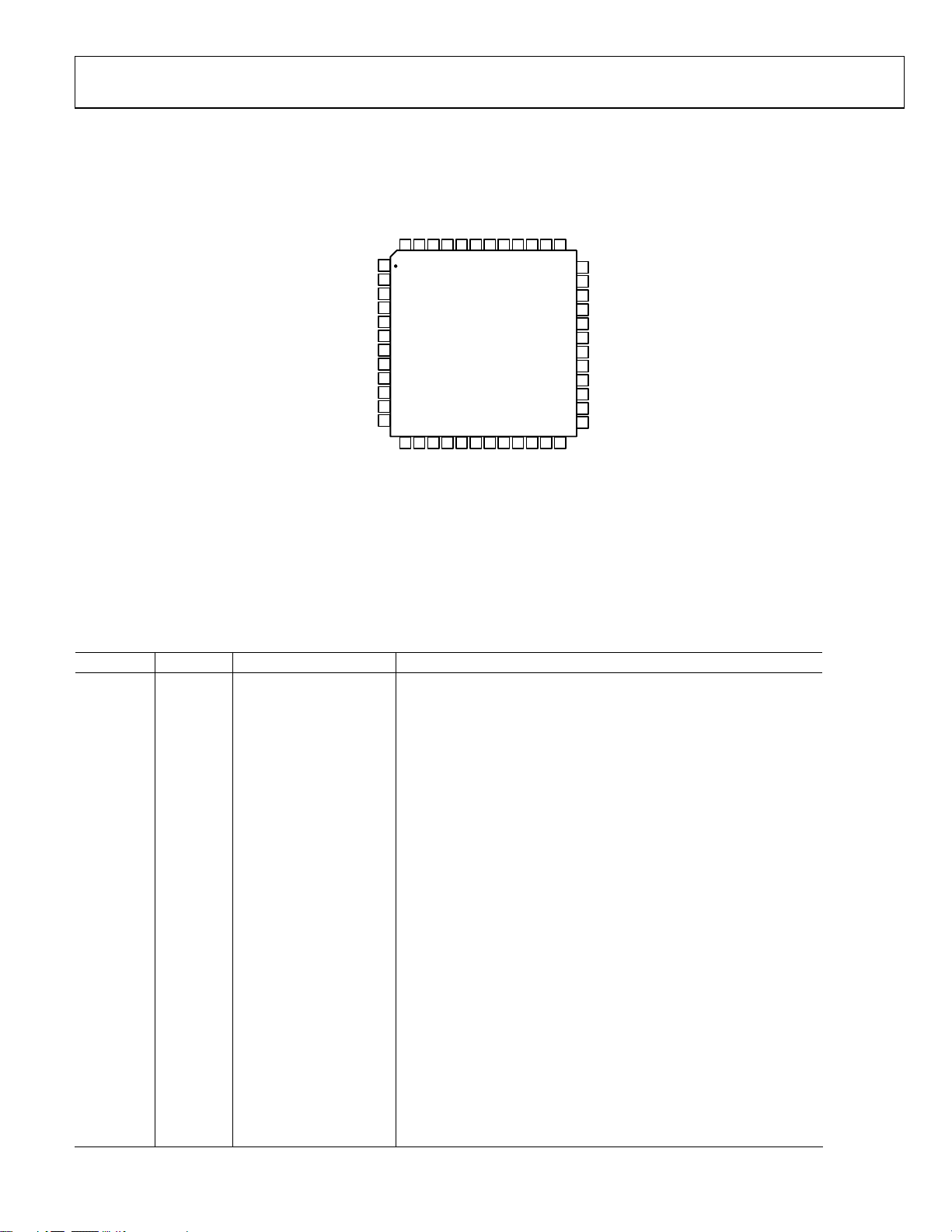
48-lead LQFP plastic package
GENERAL DESCRIPTION
The ADAU1701 is a stand-alone 28/56-bit audio DSP that
handles all system processing and control tasks. Processing
includes equalization, crossover, bass enhancement, multiband
dynamics processing, delay compensation, speaker
compensation, and stereo image widening. These algorithms
can be used to compensate for the real-world limitations of
speakers, amplifiers, and listening environments, resulting in a
dramatic improvement of perceived audio quality.
The signal processing used in the ADAU1701 is comparable to
that found in high end studio equipment. Most of the
processing is done in full 56-bit double-precision mode,
resulting in very good low level signal performance. The
ADAU1701 is a fully-programmable DSP. The easy-to-use
SigmaStudio software allows the user to graphically configure a
custom signal processing flow using blocks such as biquad
Processor with 2ADC/4DAC
ADAU1701
APPLICATIONS
Multimedia speaker systems
MP3 player speaker docks
Automotive head units
Mini-component stereos
Digital televisions
Studio monitors
Speaker crossovers
Musical instrument effects processors
In-seat sound systems (aircraft/motor coaches)
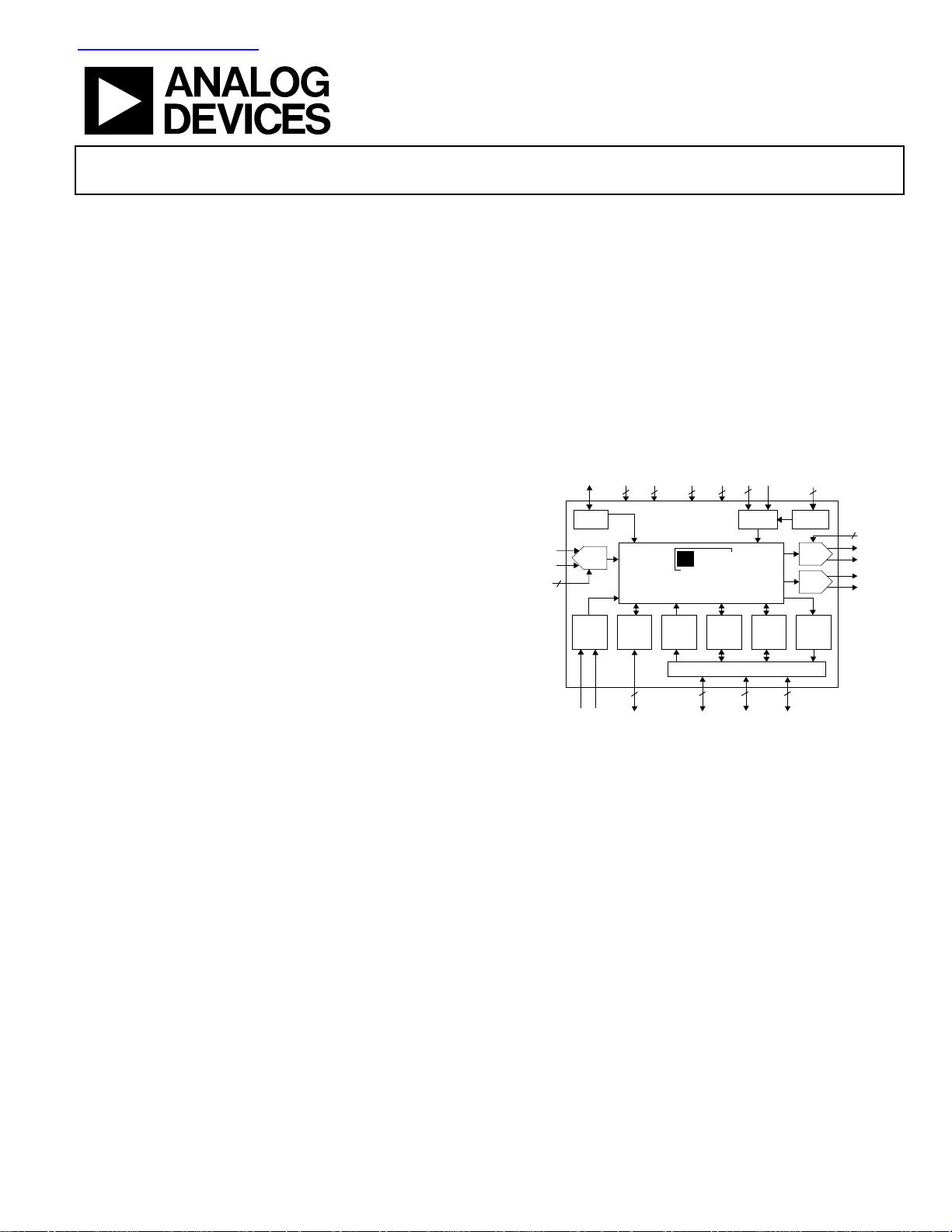
FUNCTIONAL BLOCK DIAGRAM
ANALOG
DIGITAL
2-CHANNEL
ANALOG
INPUT
FILTA/ IDAC
2
REGULATOR
RESET/
MODE
SELEC T
RESET
3.3 V
1.8 V
STEREO
ADC
SELF
BOOT
DIGITAL
VDD
CONTROL
INTER FACE
AND
SELFBO OT
I2C/SPI &
WRITEBACK
GROUND
3
3 3 3
5
ANALOG
VDD
GROUND
∑
∑
∑
DSP
PERFORMANCE AUDIO
AUDIO PRO CESSOR CORE
50 M Hz
40 ms DEL AY MEM OR Y
8-CH
DIGITAL
INPUT
8-BIT
AUX
ADC
INPUT/O UTPUT MATRIX
4 4 4
DIGITALIN
OR
GPIO
Figure 1.
filters, dynamics processors, level controls, and GPIO interface
controls.
ADAU1701 programs can be loaded on power-up either from a
serial EEPROM though its own self-boot mechanism or from
an external microcontroller. On power-down, the current state
of the parameters can be written back to the EEPROM from the
ADAU1701 to be recalled the next time the program is run.
The ADAU1701 s two ADCs and four DACs provide an analogin to analog-out dynamic range greater than 98 dB and THD+N
better than -92 dB. Digital input and output ports allow a
glueless connection to additional ADCs and DACs. The
ADAU1701 communicates through either an I
4-wire SPI port.
PLL
MODE
AUX ADC
OR
GPIO
2
PLL
GPIO
PLL
LOOP
FILTER
DIGITALOUT
GPIO
OR
CRYSTAL
2
CLOCK
OSCILLATOR
DAC
DAC
8-CH
DIGITAL
OUTPUT
2
C bus or a
FILTD/ CM
2
4-CHANNEL
ANALOG
OUTPUT
Rev. PrC
Information furnished by Analog Devices is believed to be accurate and reliable. However, no
responsibility is assumed by Anal og Devices for its use, nor for any infringements of patents or ot her
rights of third parties that may result from its use. Specifications subject to change without notice. No
license is granted by implication or otherwise under any patent or patent rights of Analog Devices.
Trademarks and registered trademarks are the property of their respective owners.
One Technology Way, P.O. Box 9106, Norwood, MA 02062-9106, U.S.A.
Tel: 781.329.4700 www.analog.com
Fax: 781.461.3113 ©2005 Analog Devices, Inc. All rights reserved.
Page 2

ADAU1701
TABLE OF CONTENTS
Features.............................................................................................. 1
Control Port Addressing ........................................................... 22
Applications....................................................................................... 1
Functional Block Diagram .............................................................. 1
General Description ......................................................................... 1
Introduction ...................................................................................... 3
Specifications..................................................................................... 4
Analog Performance .................................................................... 4
Digital I/O ..................................................................................... 5
Power.............................................................................................. 5
Temperature Range ...................................................................... 5
Digital Timing............................................................................... 5
PLL ................................................................................................. 6
Regulator........................................................................................ 6
Absolute Maximum Ratings............................................................ 7
ESD Caution.................................................................................. 7
Digital Timing Diagrams................................................................. 8
Parameter RAM.......................................................................... 22
Recommended Program/Parameter Loading Procedure..... 23
Safeload Registers....................................................................... 23
Data Capture Registers.............................................................. 23
DSP Core Control Register....................................................... 24
Interface Registers...................................................................... 24
Control Port Read/Write Data Formats .................................. 24
Multipurpose Pins.......................................................................... 27
GPIO pin Setting Register......................................................... 27
Multi-Purpose pin Configuration Registers........................... 27
Auxiliary ADC............................................................................ 27
General Purpose Input/Outputs .............................................. 28
Serial Data Input/Output Ports ................................................ 28
Serial Output Control Registers ............................................... 30
Serial Input Control Register .................................................... 31
Pin Configuration and Function Descriptions........................... 11
Pin Functions .................................................................................. 13
Signal Processing ............................................................................ 15
Overview...................................................................................... 15
Numeric Formats........................................................................ 15
Programming.............................................................................. 15
Control Port.....................................................................................16
Overview...................................................................................... 16
SPI Port........................................................................................ 16
I2C Port ........................................................................................ 16
Self boot ....................................................................................... 19
RAMs and Registers ....................................................................... 22
REVISION HISTORY
9/05—Preliminary Version PrC1
Two-Channel Audio ADC ............................................................ 33
Four-Channel DAC ........................................................................ 34
Initialization.................................................................................... 35
Power-Up Sequence ................................................................... 35
Setting Master Clock/PLL Mode.............................................. 35
Voltage Regulator ....................................................................... 35
Layout Recommendations............................................................. 36
Parts Placement .......................................................................... 36
Grounding................................................................................... 36
Outline Dimensions....................................................................... 37
Ordering Guide .......................................................................... 37
Rev. PrC | Page 2 of 39
Page 3

INTRODUCTION
The core of the ADAU1701 is a 28-bit DSP (56-bit with double
precision) optimized for audio processing. The program and
parameter RAMs can be loaded with a custom audio processing
signal flow built with ADI’s SigmaStudio graphical
programming software. The values stored in the parameter
RAM control individual signal processing blocks, such as IIR
equalization filters, dynamics processors, audio delays, and
mixer levels. A safeload feature allows parameters to be
transparently updated without causing clicks on the output
signals.
The program RAM, parameter RAM, and register contents can
be saved in an external EEPROM, from which the ADAU1701
can self-boot on start-up. In this stand-alone mode, parameters
can be controlled through the on-board multipurpose pins.
The ADAU1701 can accept controls from switches,
potentiometers, rotary encoders, and IR receivers. Parameters
such as volume and tone settings can be saved to the EEPROM
on power-down and recalled when it is powered up again.
The ADAU1701 can operate with either digital I/Os, analog
I/Os, or a mix of both. The stereo ADC and four-channel DAC
have an analog-to-analog SNR of 97 dB. … The flexible serial
data input/output ports allow for glueless interconnection to a
variety of ADCs, DACs, general-purpose DSPs, S/PDIF
receivers & transmitters, and sample rate converters. The
ADAU1701 can be configured in I
justified, or TDM serial port compatible modes.
Twelve multi-purpose (MP) pins allow for the ADAU1701 to
input external control signals and output flags or controls to
other devices in the system. These MP pins can be configured
as digital I/Os, inputs to the 4-channel auxiliary ADC, or set up
as the serial data I/O ports. As inputs, they can be connected to
buttons, switches, rotary encoders, potentiometers, IR receivers,
or other external control circuitry to control the internal signal
processing program. When configured as outputs, these pins
can be used to drive LEDs (with a buffer), control other ICs, or
connect to other external circuitry in an application.
The ADAU1701 has a sophisticated control port that supports
complete read/write capability of all memory locations. Control
registers are provided to offer complete control of the chip’s
configuration and serial modes. Handshaking is included for
ease of memory uploads and downloads. The ADAU1701 can
be configured for either SPI or I
An on-board oscillator can be connected to an external crystal
to generate the master clock. Also, a master clock phase-locked
loop (PLL) allows the ADAU1701 to be clocked from a variety
of different clock speeds. The PLL can accept inputs of 64 × f
2
S, left-justified, right-
2
C control.
,
S
ADAU1701
256 × f
, 384 × fS, or 512 × fS to generate the core’s internal
S
master clock.
The SigmaStudio software is used to program and control the
SigmaDSP through the control port. Along with designing and
tuning a signal flow, the tools can configure the all registers and
burn a new program into the external EEPROM. SigmaStudio’s
graphical interface allows anyone with digital or analog audio
processing knowledge to easily design a DSP signal flow and
port it to a target application. It also provides enough flexibility
and programmability for an experienced DSP programmer to
have in-depth control of the design. In SigmaStudio, the user
can simply connect graphical blocks such as biquad filters,
dynamics processors, mixers, and delays, compile the design,
and load the program and parameter files into the ADAU1701’s
memory through the control port. Signal processing blocks
available in the provided libraries include
• Single- and double-precision biquad filters
• Mono and multichannel dynamics processors with peak or
RMS detection
• Mixers and splitters
• Tone and noise generators
• Fixed and variable gain
• Loudness
• Delay
• Stereo enhancement
• Dynamic bass boost
• Noise and tone sources
• Level detectors
• GPIO control & conditioning
More processing blocks are always in development. Analog
Devices also provides proprietary and third-party algorithms
for applications such as matrix decoding, bass enhancement,
and surround virtualizers. Please contact ADI for information
about licensing these algorithms.
The ADAU1701 operates from a 1.8 V digital power supply and
a 3.3 V analog supply. An on-board voltage regulator can be
used to operate the digital circuitry from a 3.3 V supply. It is
fabricated on a single monolithic integrated circuit and is
housed in a 48-lead LQFP package for operation over the –0°C
to +70°C temperature range.
Rev. PrC | Page 3 of 39
Page 4
ADAU1701
SPECIFICATIONS
Test conditions, unless otherwise noted.
Table 1.
Parameter Conditions
Analog Supply Voltage (AVDD)
Digital Supply Voltage (DVDD)
PLL Voltage (PVDD)
Output Voltage (IOVDD)
Ambient Temperature
Master Clock Input
Load Capacitance
Load Current
Input Voltage, HI
Input Voltage, LO
ANALOG PERFORMANCE
Table 2. Analog Performance
Parameter Min Typical Max Units Test Conditions/Comments
REFERENCE SECTION
Absolute Voltage V
V
Temperature Coefficient TBD ppm/°C
REF
AUX ANALOG INPUTS
Full Scale Analog Input 3.3 V
Step size 13 mV
ADC INPUTS
Number of channels 2 Stereo ADC
Resolution 24 Bits
Full Scale Analog Input
Signal-to-Noise Ratio
A-Weighted 100 dB
Dynamic Range -60dB with respect to full scale Analog input
A-Weighted TBD dB
Total Harmonic Distortion + Noise -95 dB -xxdB with respect to full scale Analog input
Interchannel Gain Mismatch TBD dB Left and Right channel Gain Mismatch
Crosstalk TBD dB Analog Channel Crosstalk
DC Bias TBD V
Gain Error TBD dB
Power Supply Rejection TBD dB 1kHz, 300mV
DAC OUTPUTS
Number of channels 4 2 stereo output channels
Resolution 24 Bits
Full Scale Analog Output 1 Vrms
Signal-to-Noise Ratio
A-Weighted 105 dB
Dynamic Range -60dB with respect to full scale Analog input
A-Weighted TBD dB
Total Harmonic Distortion + Noise -95 dB -xxdB with respect to full scale Analog input
Crosstalk TBD dB Analog Channel Crosstalk
Interchannel Gain Mismatch TBD dB Left and Right channel Gain Mismatch
DC Bias 1.5 V
Power Supply Rejection TBD dB 1kHz, 300mV
1.5 V
REF
100
μArms
2Vrms input with 20kΩ series resistor
Signal at AVDD
P-P
Signal at AVDD
P-P
Rev. PrC | Page 4 of 39
Page 5
ADAU1701
DIGITAL I/O
Table 3. Digital I/O
Parameter Min Max Unit
Input Voltage, HI (VIH) V
Input Voltage, LO (VIL) V
Input Leakage (IIH) μA
Input Leakage (IIL) μA
Low Level Output Voltage (VOL) IOVDD = x.x V, IOL = xx mA V
Low Level Output Voltage (VOL) IOVDD = x.x V, IOL = xx mA V
Input Capacitance pF
POWER
Table 4.
Parameter Comments Min Typ Max1 Unit
Supplies
Analog Voltage 3.3 V
Digital Voltage 1.8 V
PLL Voltage 3.3 V
Analog Current TBD mA
Digital Current TBD mA
PLL Current TBD mA
Analog Current, Reset TBD mA
Digital Current, Reset TBD mA
PLL Current, Reset TBD mA
Dissipation
Operation, all supplies TBD mW
Reset, all supplies TBD mW
1
Maximum specifications are measured across −xx°C to xx°C (case) and across VDD = xxx V to xxx V.
TEMPERATURE RANGE
Table 5.
Parameter Min Typ Max Unit
Functionality Guaranteed xx°C xx°C °C Ambient
xx°C xx°C °C Case
DIGITAL TIMING
Table 6 Digital Timing1
Parameter Comments Min Max Unit
tMP MCLK Period 512 fS mode ns
tMP MCLK Period 384 fS mode ns
tMP MCLK Period 256 fS mode ns
tMP MCLK Period 64 fS mode ns
tMP MCLK Period Bypass mode ns
t
MCLK Duty Cycle Bypass mode %
MDC
t
BCLK_IN LO Pulse Width ns
BIL
t
BCLK_IN HI Pulse Width ns
BIH
t
LRCLK_IN Setup To BCLK_IN rising ns
LIS
t
LRCLK_IN Hold From BCLK_IN rising ns
LIH
t
SDATA_INx Setup To BCLK_IN rising ns
SIS
t
SDATA_INx Hold From BCLK_IN rising ns
SIH
t
LRCLK_OUTx Setup Slave mode ns
LOS
t
LRCLK_OUTx Hold Slave mode ns
LOH
tTS
BCLK_OUTx Falling to
ns
Rev. PrC | Page 5 of 39
Page 6
ADAU1701
LRCLK_OUTx Timing Skew
t
SDATA_OUTx Delay Slave mode, from BCLK_OUTx falling ns
SODS
t
SDATA_OUTx Delay Master mode, from BCLK_OUTx falling ns
SODM
t
CCLK Pulse Width LO
CCPL
t
CCLK Pulse Width HI
CCPH
t
CLATCH Setup To CCLK rising ns
CLS
t
CLATCH Hold From CCLK rising
CLH
t
CLATCH Pulse Width HI
CLPH
t
CDATA Setup To CCLK rising ns
CDS
t
CDATA Hold From CCLK rising
CDH
t
COUT Delay From CCLK rising
COD
t
RESETB LO Pulse Width ns
RLPW
f
SCL Clock Frequency TBD kHz
SCL
t
SCL High TBD μS
SCLH
t
SCL Low TBD μS
SCLL
t
Setup Time Relevant for Repeated Start Condition TBD μS
SCS
t
Hold Time
SCH
After this period the 1st clock is
ns
ns
ns
ns
ns
ns
TBD μS
generated
tDS Data Setup Time TBD ns
t
SCL Rise Time TBD ns
SCR
t
SCL Fall Time TBD ns
SCF
t
SDA Rise Time TBD ns
SDR
t
SDA Fall Time TBD ns
SDF
1
All timing specifications are given for the default (I2S) states of the serial input control port and the serial output control ports. See
Table 40.
PLL
Table 7.
Parameter Min Typ Max Unit
Lock Time TBD ms
REGULATOR
Table 8.
Parameter Min Typ Max Unit
DVDD Voltage 1.8 V
Rev. PrC | Page 6 of 39
Page 7
ADAU1701
ABSOLUTE MAXIMUM RATINGS
Table 9.
Parameter Min Max Unit
DVDD to GND V
AVDD to GND V
IOVDD to GND V
Digital Inputs V
Maximum Junction Temperature 135 °C
Storage Temperature Range –65 +150 °C
Soldering (10 sec) 300 °C
Stresses above those listed under Absolute Maximum Ratings may cause permanent damage to the device. This is a stress rating only;
functional operation of the device at these or any other conditions above those indicated in the operational section of this specification is
not implied. Exposure to absolute maximum rating conditions for extended periods may affect device reliability.
Table 10. Package Characteristics
Parameter Min Typ Max Unit
θJA Thermal Resistance (Junction-to-Ambient) 72 °C/W
θJC Thermal Resistance (Junction-to-Case) 19.5 °C/W
ESD CAUTION
ESD (electrostatic discharge) sensitive device. Electrostatic charges as high as 4000 V readily accumulate on
the human body and test equipment and can discharge without detection. Although this product features
proprietary ESD protection circuitry, permanent damage may occur on devices subjected to high energy
electrostatic discharges. Therefore, proper ESD precautions are recommended to avoid performance
degradation or loss of functionality.
Rev. PrC | Page 7 of 39
Page 8
ADAU1701
TYPICAL PERFORMANCE CHARACTERISTICS
Figure 2
Figure 3
Figure 5
Figure 6
Figure 4
Rev. PrC | Page 8 of 39
Page 9
DIGITAL TIMING DIAGRAMS
t
BIH
BCLK_IN
t
BIL
t
LIS
LRCLK_IN
t
SDATA_INX
LEFT-JUSTIFIED
MODE
SDATA_INX
2
I
S-JUSTIFIED
MODE
SDATA_INX
RIGHT-JUSTIFIED
MODE
SIS
MSB
t
SIH
8-BIT CLOCKS
(24-BIT DATA)
12-BIT CLOCKS
(20-BIT DATA)
14-BIT CLOCKS
(18-BIT DATA)
16-BIT CLOCKS
(16-BIT DATA)
t
SIS
MSB-1
MSB
t
SIH
Figure 7. Serial Input Port Timing
ADAU1701
t
SIS
MSB
t
SIH
t
LIH
t
SIS
LSB
t
SIH
04607-0-013
BCLK_OUTX
LRCLK_OUTX
SDATA_OUTX
LEFT-JUSTIFIED
RIGHT-JUSTIFIED
MODE
SDATA_OUTX
2
I
S-JUSTIFIED
MODE
SDATA_OUTX
MODE
t
t
BIH
t
BIL
t
LOS
t
SDDS
t
SDDM
MSB
8-BIT CLOCKS
(24-BIT DATA)
12-BIT CLOCKS
(20-BIT DATA)
14-BIT CLOCKS
(18-BIT DATA)
16-BIT CLOCKS
(16-BIT DATA)
t
SDDS
t
SDDM
MSB-1
MSB
t
SDDS
t
SDDM
MSB
Figure 8. Serial Output Port Timing
LCH
LSB
t
TS
04607-0-014
Rev. PrC | Page 9 of 39
Page 10
ADAU1701
CLATCH
CCLK
CDATA
COUT
t
CLS
t
CCPL
t
CDS
t
CCPH
t
CDH
Figure 9. SPI Port Timing
t
CLH
t
COD
t
CLPH
04607-0-015
t
DS
t
SCLH
t
ST
Figure 10. I
2
C Port Timing
t
TSCH
t
SCS
t
SSH
04607-026
SDA
SCLK
t
TSCH
t
SR
t
SCLL
t
MP
MCLK
RESETB
t
RLPW
Figure 11. Master Clock and Reset Timing
04607-0-016
Rev. PrC | Page 10 of 39
Page 11
PIN CONFIGURATION AND FUNCTION DESCRIPTIONS
0
1
E
E
D
D
O
O
M
M
D
D
_
_
T
N
G
A
1
1
P
M
L
L
L
M
L
L
I
P
F
P
C
T
K
P
G
I
L
U
R
/W
C
O
T
H
C
/C
_
/
C
L
B
A
T
C
D
W
A
S
/
S
L
A
C
T
A
D
C
/
1
R
D
D
A
AGND
ADC1
ADC_RES
ADC0
RESETB
SELFBOOT
ADDR0
MP4
MP5
MP1
MP0
DGND
A
T
D
V
IL
A
F
48 47 46 45 44 39 38 3743 42 4 1 40
1
2
3
4
5
6
7
8
9
10
11
12
13 14 15 16 17 18 19 20 21 22 23 24
7
D
P
D
M
V
D
U
U
U
O
O
O
V
V
V
ADAU1701
TOP VIEW
(Not to Scale)
6
0
1
P
P
M
M
U
O
V
E
D
D
IV
V
R
D
IO
V
3
2
1
0
T
T
T
T
D
Figure 12. 48-Lead LQFP Pin Configuration
ADAU1701
D
N
G
A
36
AVDD
35
PLL_LF
34
PVDD
33
PGND
32
MCLKI
31
OSCO
30
RSVD
MP2
29
MP3
28
27
MP8
26
MP9
25
DGND
D
D
V
D
Table 11. Pin Function Descriptions
Pin No. I/O Mnemonic Description
1 AGND Analog Ground
2 IN ADC1 Analog input 1
3 ADC_RES Reference current – connect resistor
4 IN ADC0 Analog Input 0
5 IN RESETB Reset, Active Low
6 IN SELFBOOT Select Host or Self-boot mode
7 IN ADDR0 I2C and SPI Address 0
8 IN/OUT MP4 Multi-Purpose – GPIO or Serial input port LRCLK
9 IN/OUT MP5 Multi-Purpose – GPIO or Serial input port BCLK
10 IN/OUT MP1 Multi-Purpose – GPIO or Serial Input port data 1
11 IN/OUT MP0 Multi-Purpose – GPIO or Serial Input port data 0
12 DGND Digital Ground
13 DVDD 1.8 V Digital Supply
14 IN/OUT MP7 Multi-Purpose – GPIO or Serial output port data 1
15 IN/OUT MP6 Multi-Purpose – GPIO, Serial output port data 0, or TDM data output
16 IN/OUT MP10 Multi-Purpose – GPIO or Serial output port LRCLK
17 OUT VDRIVE Drive for external PNP Transistor for 1.8 V regulator
18 IOVDD Input and Output Pin Supply
19 IN/OUT MP11 Multi-Purpose – GPIO or Serial output port BCLK
20 IN ADDR1/CDATA/WB_TRIG I2C Address 1 / SPI Data Input / Self-boot Write-back trigger
21 IN/OUT CLATCH / WP SPI Latch / Self-boot EEPROM write protect
22 IN/OUT SDA/COUT I2C Data / SPI Data Out
23 IN/OUT SCL/CCLK I2C Clock / SPI Clock
24 DVDD 1.8 V Digital Supply
25 DGND Digital Ground
Rev. PrC | Page 11 of 39
Page 12

ADAU1701
26 IN/OUT MP9 Multi-Purpose – GPIO or Aux ADC input 0
27 IN/OUT MP8 Multi-Purpose – GPIO or Aux ADC input 3
28 IN/OUT MP3 Multi-Purpose – GPIO or Aux ADC input 2
29 IN/OUT MP2 Multi-Purpose – GPIO or Aux ADC input 1
30 RSVD Reserved, tie to ground
31 OUT OSCO Oscillator Output
32 IN MCLKI Master Clock or Crystal Input
33 PGND PLL Ground
34 PVDD 3.3 V PLL Power
35 PLL_LF PLL Loop Filter connection
36 AVDD 3.3 V Analog Supply
37 AGND Analog Ground
38 IN PLL_MODE0 PLL Mode select 0
39 IN PLL_MODE1 PLL Mode select 1
40 CM Common Mode Decoupling Capacitor
41 FILTD Decoupling Capacitor
42 AGND Analog Ground
43 OUT VOUT3 Channel 3 DAC output
44 OUT VOUT2 Channel 2 DAC output
45 OUT VOUT1 Channel 1 DAC output
46 OUT VOUT0 Channel 0 DAC output
47 FILTA Decoupling capacitor
48 AVDD 3.3 V Analog Supply
Rev. PrC | Page 12 of 39
Page 13

PIN FUNCTIONS
Table 11 shows the ADAU1701’s pin numbers, names, and
functions. Input pins have a logic threshold compatible with
TTL input levels and may be used in systems with 3.3 V logic.
ADAU1701
SDA
I2C Serial Data. The data line is bidirectional. The line
connected to this pin should have a 2 kΩ pull-up resistor on it.
ADC0
ADC1
Stereo ADC inputs.
IDAC
Bias current pin for ADC. A resistor with the same value as
those on the ADC0 & ADC1 should be connected between this
pin and ground.
FILTA
ADC decoupling pin. A 10 μF capacitor should be placed
between this pin and ground.
VOUT0
VOUT1
VOUT2
VOUT3
Four-channel DAC outputs
CM
Reference. A 47 μF capacitor should be placed between this pin
and ground to reduce crosstalk.
FILTD
DAC decoupling pin. A 10 μF capacitor should be placed
between this pin and ground.
PLL_MODE0
PLL_MODE1
PLL Mode Control Pins. The functionality of these pins is
described in the Setting Master Clock/PLL Mode section.
MCLKI
Master clock or crystal oscillator input.
OSCO
Crystal oscillator output.
PLL_LF
PLL loop filter connection.
SCL
I2C Clock. This pin is always an input when in I2C control
mode. In self-boot mode this pin will be an output (I
master). The line connected to this pin should have a 2 kΩ
pull-up resistor on it.
2
C
CDATA
Serial Data Input for the SPI Control Port.
COUT
Serial Data Output for the SPI Port. This is used for reading
back registers and memory locations. It is three-stated when an
SPI read is not active.
CCLK
SPI Bit Clock. This clock may either run continuously or be
gated off in between SPI transactions.
CLATCH
SPI Latch Signal. This must go low at the beginning of an SPI
transaction and high at the end of a transaction. Each SPI
transaction may take a different number of CCLKs to complete,
depending on the address and read/write bit that are sent at the
beginning of the SPI transaction.
ADDR0
ADDR1
Address Select. These pins select the address for the
ADAU1701’s communication with the control port. This allows
two ADAU1701s to be used on the same control port.
WP
EEPROM write protect.
WB_TRIG
EEPROM Writeback trigger.
RESETB
Active-Low Reset Signal. After RESETB goes high, the
ADAU1701 goes through an initialization sequence where the
program and parameter RAMs are initialized with the contents
of the on-board boot ROMs. All registers are set to 0, and the
data RAMs are also set to 0. The initialization is complete after
xxxx internal MCLK cycles (referenced to the rising edge of
RESETB), which corresponds to xxxx external MCLK cycles if
the part is in 256 × f
to the control port until the initialization is complete.
mode. New values should not be written
S
SELFBOOT
Selfboot or external program load select.
Rev. PrC | Page 13 of 39
Page 14

ADAU1701
MP0
MP1
MP2
MP3
MP4
MP5
MP6
MP7
MP8
MP9
MP10
MP11
Multi-purpose input/output pins. These pins can be configured
as serial data inputs/outputs, auxiliary ADC inputs, or general
purpose switch and button inputs/outputs.
DVDD
Digital VDD for Core. 1.8 V nominal.
DGND
Digital Ground.
IOVDD
Input and Output pins supply.
PVDD
PLL and aux ADC supply.
PGND
PLL and aux ADC ground.
VDRIVE
Drive for External Transistor. The base of the voltage regulator’s
external PNP transistor is driven from this pin.
AVDD
Analog VDD for Core. 3.3 V nominal.
AGND
Analog Ground.
RSVD
This pin should be tied to ground.
Rev. PrC | Page 14 of 39
Page 15

SIGNAL PROCESSING
OVERVIEW
The ADAU1701 is designed to provide all signal processing
functions commonly used in stereo or multichannel playback
systems. The signal processing flow is designed using the ADIsupplied SigmaStudio software, which allows graphical entry
and real-time control of all signal processing functions.
Many of the signal processing functions are coded using full,
56-bit double-precision arithmetic. The input and output word
lengths are 24 bits. Four extra headroom bits are used in the
processor to allow internal gains up to 24 dB without clipping.
Additional gains can be achieved by initially scaling down the
input signal in the signal flow.
The signal processing blocks can be arranged in a custom program that can be loaded to the ADAU1701’s RAM. The
available signal processing blocks are explained in the following
sections.
NUMERIC FORMATS
It is common in DSP systems to use a standardized method of
specifying numeric formats. Fractional number systems are
specified by an A.B format, where A is the number of bits to the
left of the decimal point and B is the number of bits to the right
of the decimal point.
The ADAU1701 uses the same numeric format for both the
coefficient values (stored in the parameter RAM) and the signal
data values. The format is as follows:
Numerical Format: 5.23
Range: –16.0 to (+16.0 − 1 LSB)
Examples:
1000 0000 0000 0000 0000 0000 0000 = –16.0
1110 0000 0000 0000 0000 0000 0000 = –4.0
1111 1000 0000 0000 0000 0000 0000 = –1.0
ADAU1701
1111 1110 0000 0000 0000 0000 0000 = –0.25
1111 1111 1111 1111 1111 1111 1111 = (1 LSB below 0.0)
0000 0000 0000 0000 0000 0000 0000 = 0.0
0000 0010 0000 0000 0000 0000 0000 = 0.25
0000 1000 0000 0000 0000 0000 0000 = 1.0
0010 0000 0000 0000 0000 0000 0000 = 4.0
0111 1111 1111 1111 1111 1111 1111 = (16.0 – 1 LSB).
The serial port accepts up to 24 bits on the input and is signextended to the full 28 bits of the core. This allows internal
gains of up to 24 dB without encountering internal clipping.
A digital clipper circuit is used between the output of the DSP
core and the outputs (see Figure 13). This clips the top four bits
of the signal to produce a 24-bit output with a range of 1.0
(minus 1 LSB) to –1.0.
4-BIT SIGN EXTENSION
DATA IN SERIAL PORT
1.23 5.23
Figure 13. Numeric Precision and Clipping Structure
SIGNAL PROCESSING
(5.23 FORMAT)
PROGRAMMING
On power-up, the ADAU1701’s default program passes the
unprocessed input signals to the outputs (Figure 27), but the
outputs are muted by default (see Power-Up Sequence section).
There are 1,024 instruction cycles per audio sample, resulting in
an internal clock rate of 49.152 MHz (for f
runs in a stream-oriented manner, meaning all 1,024
instructions are executed each sample period. The ADAU1701
may also be set up to accept double or quad-speed inputs by
reducing the number of instructions/sample, which can be set
in the core control register.
The part can be programmed easily using SigmaStudio, a
graphical tool provided by Analog Devices. No knowledge of
writing line-level DSP code is required.
s
DIGITAL
CLIPPER
5.23 1.23
= 48 kHz). This DSP
04607-0-005
Rev. PrC | Page 15 of 39
Page 16

ADAU1701
CONTROL PORT
OVERVIEW
The ADAU1701 has many different control options that can be
set through an SPI or I
4-wire SPI control port, and a 2-wire I
power-up, the part defaults to I
SPI control mode by pulling pin CLATCH/WP low three times.
The control port is capable of full read/write operation for all of
the memories and registers. Most signal processing parameters
are controlled by writing new values to the parameter RAM
using the control port. Other functions, such as mute and
input/output mode control, are programmed by writing to the
control registers.
All addresses may be accessed in both a single-address mode or
a burst mode. A control word consists of the chip address, the
register/RAM subaddress, and the data to be written. The
number of bytes per word depends on the type of data that is
written.
The first byte of a control word (Byte 0) contains the 7-bit chip
address plus the R/W bit. The next two bytes (Bytes 1 and 2)
together form the subaddress of the memory or register
location within the ADAU1701. This subaddress needs to be
two bytes because the memories within the ADAU1701 are
directly addressable, and their sizes exceed the range of singlebyte addressing. All subsequent bytes (Bytes 3, 4, etc.) contain
the data, such as control port data or program or parameter
data. The exact formats for specific types of writes are shown in
Table 22 to Table 30.
The ADAU1701 has several mechanisms for updating signal
processing parameters in real time without causing pops or
clicks. In cases where large blocks of data need to be downloaded, the output of the DSP core can be halted (using Bit x of
the core control register), new data loaded, and then restarted.
This is typically done during the booting sequence at start-up or
when loading a new program into RAM. In cases where only a
few parameters need to be changed, they can be loaded without
halting the program. To avoid unwanted side effects while
loading parameters on the fly, the SigmaDSP provides the
safeload registers. The safeload registers can be used to buffer a
full set of parameters (e.g. the five coefficients of a biquad) and
then transfer these parameters into the active program within
one audio frame. The safeload mode uses internal logic to
prevent contention between the DSP core and the control port.
SPI PORT
The SPI port uses a 4-wire interface, consisting of CLATCH,
CCLK, CDATA, and COUT signals. The CLATCH signal goes
low at the beginning of a transaction and high at the end of a
transaction. The CCLK signal latches CDATA on a low-to-high
transition. COUT data is shifted out of the ADAU1701 on the
2
C interface. The ADAU1701 has both a
2
C bus control port. At
2
C mode, but can be put into
falling edge of CCLK and should be clocked into the receiving
device, such as a microcontroller, on CCLK’s rising edge. The
CDATA signal carries the serial input data, and the COUT
signal is the serial output data. The COUT signal remains threestated until a read operation is requested. This allows other SPIcompatible peripherals to share the same readback line. All SPI
transactions follow the same basic format, shown in Table 12. A
timing diagram is shown in Figure 9. All data written should be
MSB-first.
Table 12. Generic Control Word Format
Byte 4,
Byte 0 Byte 1 Byte 2 Byte 3
chip_adr [6:0],
R/W
0000,
subadr
[11:8]
subadr[7:0] data data
etc.
Chip Address R/W
The first byte of an SPI transaction includes the 7-bit chip
address and a R/
bit. The chip address is set by the ADR_SEL
W
pin. This allows two ADAU1701s to share a CLATCH signal,
yet still operate independently. When ADR_SEL is low, the chip
address is 0000000; when it is high, the address is 0000001. The
LSB of this first byte determines whether the SPI transaction is
a read (Logic Level 1) or a write (Logic Level 0).
Subaddress
The 12-bit Subaddress word is decoded into a location in one of
the memories or registers. This subaddress is the location of the
appropriate RAM location or register.
Data Bytes
The number of data bytes varies according to the register or
memory being accessed. In burst write mode, an initial
subaddress is given followed by a continuous sequence of data
for consecutive memory/register locations. The detailed data
format diagram for continuous-mode operation is given in the
Control Port Read/Write Data Formats section.
A sample timing diagram for a single SPI write operation to the
parameter RAM is shown in Figure 14. A sample timing
diagram of a single SPI read operation is shown in Figure 15.
The COUT pin goes from three-state to driven at the beginning
of Byte 3. In this example, Bytes 0 to 2 contain the addresses and
R/W bit, and subsequent bytes carry the data.
I2C PORT
The ADAU1701 supports a 2-wire serial (I2C compatible)
micro-processor bus driving multiple peripherals. Two pins,
serial data (SDA) and serial clock (SCL), carry information
between the ADAU1701 and the system I
The ADAU1701 is always a slave on the I
that it will never initiate a data transfer. Each slave device is
2
C master controller.
2
C bus, which means
Rev. PrC | Page 16 of 39
Page 17

recognized by a unique address. The address byte format is
shown in Table 13. The ADAU1701 has four possible slave
addresses: two for writing operations and two for reading.
These are unique addresses for the device and are illustrated in
Table 14. The LSB of the byte sets either a read or write
operation; Logic Level 1 corresponds to a read operation, and
Logic Level 0 corresponds to a write operation. The sixth and
seventh bits of the address are set by tying the ADDRx pins of
the ADAU1701 to logic level 0 or logic level 1.
Table 13. ADAU1701 Address Byte Format
Bit 0 Bit 1 Bit 2 Bit 3 Bit 4 Bit 5 Bit 6 Bit 7
0 1 1 0 1 ADDR1 ADDR0
R/W
Table 14. ADAU1701 I2C Addresses
ADDR1 ADDR0
0 0 0 0x68
0 0 1 0x69
0 1 0 0x6A
0 1 1 0x6B
1 0 0 0x6C
1 0 1 0x6D
1 1 0 0x6E
1 1 1 0x6F
Read/
Write
Slave Address
Addressing
Initially, all devices on the I2C bus are in an idle state, which is
where the devices monitor the SDA and SCL lines for a start
condition and the proper address. The I
2
C master initiates a
data transfer by establishing a Start condition, defined by a
high-to-low transition on SDA while SCL remains high. This
indicates that an address/data stream will follow. All devices on
the bus respond to the start condition and shift the next eight
bits (7-bit address + R/
bit) MSB first. The device that
W
recognizes the transmitted address responds by pulling the data
line low during the ninth clock pulse. This ninth bit is known as
an acknowledge bit. All other devices withdraw from the bus at
this point and return to the idle condition. The R/
W
bit
determines the direction of the data. A logic 0 on the LSB of the
first byte means the master will write information to the
peripheral. A logic 1 on the LSB of the first byte means the
master will read information from the peripheral. A data
transfer takes place until a stop condition is encountered. A stop
condition occurs when SDA transitions from low to high while
2
SCL is held high. Figure 16 shows the timing of an I
C write.
Burst mode addressing, where the subaddresses are automatically incremented at word boundaries, can be used for writing
large amounts of data to contiguous memory locations. This
increment happens automatically if a stop condition is not
encountered after a single-word write. The registers and
memories in the ADAU1701 range in width from one to five
bytes, so the autoincrement feature knows the mapping between
ADAU1701
sub-addresses and the word length of the destination register
(or memory location). A data transfer is always terminated by a
stop condition.
Stop and start conditions can be detected at any stage during
the data transfer. If these conditions are asserted out of
sequence with normal read and write operations, these cause an
immediate jump to the idle condition. During a given SCL high
period, the user should only issue one start condition, one stop
condition, or a single stop condition followed by a single start
condition. If an invalid subaddress is issued by the user, the
ADAU1701 does not issue an acknowledge and returns to the
idle condition. If the user exceeds the highest subaddress while
in autoincrement mode, one of two actions will be taken. In
read mode, the ADAU1701 outputs the highest subaddress
register contents until the master device issues a noacknowledge, indicating the end of a read. A no-acknowledge
condition is where the SDA line is not pulled low on the ninth
clock pulse on SCL. If the highest subaddress location is
reached while in write mode, the data for the invalid byte is not
loaded into any subaddress register, a no-acknowledge is issued
by the ADAU1701, and the part returns to the idle condition.
I2C Read & Write Operations
Figure 18 shows the timing of a single-word write operation.
Every ninth clock, the ADAU1701 issues an acknowledge by
pulling SDA low.
Figure 19 shows the timing of a burst mode write sequence.
This figure shows an example where the target destination
registers are two bytes. The ADAU1701 knows to increment its
subaddress register every two bytes because the requested
subaddress corresponds to a register or memory area with a
2-byte word length.
The timing of a single word read operation is shown in
Figure 20. Note that the first R/
bit is still a 0, indicating a
W
write operation. This is because the subaddress still needs to be
written in order to set up the internal address. After the
ADAU1701 acknowledges the receipt of the subaddress, the
master must issue a repeated start command followed by the
chip address byte with the R/
set to 1 (read). This causes the
W
ADAU1701’s SDA to turn around and begin driving data back
to the master. The master then responds every ninth pulse with
an acknowledge pulse to the ADAU1701.
Figure 21 shows the timing of a burst-mode read sequence. This
figure shows an example where the target read registers are two
bytes. The ADAU1701 knows to increment its subaddress
register every two bytes because the requested subaddress
corresponds to a register or memory area with word lengths of
two bytes. Other address ranges may have a variety of word
lengths ranging from one to five bytes; the ADAU1701 always
decodes the subaddress and sets the autoincrement circuit so
Rev. PrC | Page 17 of 39
Page 18

ADAU1701
that the address increments after the appropriate number of
bytes.
CLATCH
CCLK
CDATA
BYTE 0 BYTE 1 BYTE 2 BYTE 3
04607-0-006
Figure 14. SPI Write format (Single-Write Mode)
CLATCH
CCLK
CDATA
COUT
BYTE 0
HI-Z
BYTE 1
DATA
DATA DATA
HI-Z
04607-0-007
Figure 15. SPI Read Format (Single-Read Mode)
SCK
SDA
START BY
MASTER
0
00 0
00
FRAME 1
CHIP ADDRESS BYTE
ADR
SEL
R/W
ADAU1421
ACK. BY
FRAME 2
SUBADDRESS BYTE 1
ACK. BY
ADAU1421
SCK
(CONTINUED)
SDA
(CONTINUED)
FRAME 2
SUBADDRESS BYTE 2
ACK. BY
ADAU1421
FRAME 3
DATA BYTE 1
ACK. BY
ADAU1421
STOP BY
MASTER
Figure 16. ADAU1701 I2C Write Format
Rev. PrC | Page 18 of 39
Page 19

ADAU1701
SCK
S
SDA
START BY
MASTER
SCK
(CONTINUED)
SDA
(CONTINUED)
SCK
(CONTINUED)
SDA
(CONTINUED)
Chip
Address,
= 0
R/W
AS
CHIP ADDRESS BYTE
SUBADDRESS BYTE 2
READ DATA BYTE 1
Subaddress
High
FRAME 1
FRAME 3
FRAME 5
AS
ADR
R/W
SEL
Figure 17. ADAU1701 I2C Read Format
Subaddress
Low
ACK. BY
ADAU1421
ACK. BY
ACK. BY
MASTER
REPEATED
START BY
MASTER
AS
Data Byte
ADAU1421
1
Figure 18. Single-Word I2C Write
FRAME 2
SUBADDRESS BYTE 1
FRAME 4
CHIP ADDRESS BYTE
FRAME 6
READ DATA BYTE 2
AS
Data Byte
2
ACK. BY
ADAU1421
ADR
SEL
ACK. BY
MASTER
… AS
R/W
ACK. BY
ADAU1421
STOP BY
MASTER
Data Byte
N
P
Chip
Address,
W
= 0
R/
Subaddress
High
Subaddress
Low
Figure 19. Burst Mode I2C Write
S
Chip
Address,
= 0
R/W
AS
Subaddress
High
AS
Subaddress
Low
AS S
Figure 20. Single Word I2C Read
S
Chip
Address,
= 0
R/W
S - Start Bit
P - Stop Bit
AM - Acknowledge by Master
AS - Acknowledge by Slave
AS
Subaddress
High
AS
Subaddress
Low
Figure 21. Burst Mode I2C Read
SELF BOOT
The ADAU1701 can load a set of program and parameters that
has been saved in an external EEPROM on power-up.
Data
Word
1,
Byte 1
Chip
Address,
R/W
AS S
Data
Word 1,
Byte 2
AS
Data
Byte 1
AM
Data
Word 2,
Byte 1
Data
Byte 2
Data
Word 2,
Byte 2
… AM
Data
Byte N
= 1
Chip
Address,
R/W = 1
AS
Data
Word 1,
Byte 1
AM
Data
Word 1,
Byte 2
AM … P
Combined with the auxiliary ADC and the GPIO pins, this
eliminates the need for a microcontroller in the system. The
self-booting is accomplished by the ADAU1701 acting as a
P
Rev. PrC | Page 19 of 39
Page 20

ADAU1701
master on the I2C bus on start-up, which occurs when the
Selfboot pin is set high. The ADAU1701 cannot self-boot in
SPI mode.
The maximum necessary EEPROM size is about 9 kB. This
much memory will only be needed if the program RAM (1024
× 5 bytes), parameter RAM (1024 × 4 bytes), and interface
registers (8 × 4 bytes) are each completely full. In most
applications, an 8 kB EEPROM will be sufficient.
2
Pin I
C Mode SPI Mode Selfboot
Mode
EEPROM format
The EEPROM contains a sequence of messages. Each message
may be one of:
Write bytes
Delay
Set write back multiple times
Set write back falling edge sensitive
End of messages
SCL/CCLK SCL - input CCLK -
SCL - output
input
SDA/COUT SDA – open
collector
output
ADDR1/CDAT
ADDR1 - input CDATA -
A/WB_TRIG
CLATCH/WP unused input –
tie to ground
or VDD
COUT –
output
input
CLATCH
- input
SDA – open
collector
output
trigger
writeback
EEPROM
Write Protect
- open
collector
output
Also used as
input. Attach
resistor to
3.3V VDD
ADDR0 ADDR0 - input ADDR0 -
input
unused input
– tie to
ground or
VDD
A selfboot operation is triggered on the rising edge of RESETB
when the SELFBOOT and WP pins are set high. The
ADAU1701 reads a program, parameters, and register settings
from the EEPROM. Once the ADAU1701 has finished
selfbooting, further messages may be sent to the ADAU1701 on
2
C bus, although this typically won’t be necessary in a
the I
selfbooting application. The I
write and 0x69 for a read in this mode. The ADDRx pins have
different functions if the chip is used in this mode, so the
settings on them are ignored.
The ADAU1701 will selfbooot only if WP is set low. This
allows the EEPROM to be programmed in-circuit. The WP
signal must be pulled low (it would normally have a resistor
pull-up) to enable writes to the EEPROM and this disables
selfboot until WP is taken high.
2
C device address is 0x68 for a
End of messages and wait for a writeback
No-op message
Each message consists of a sequence of one or more bytes. The
first byte determines the message type and must be one of the
following shown in Table 15. Bytes are written MSB-first.
Table 15. EEPROM Message Types
Message Byte Message Type Following Bytes
0x00 End none
0x01 Write 2 bytes for length
followed by data bytes
0x02 Delay 2 bytes for delay
0x03 No-Op none
0x04 Set multiple write
none
back
0x05 Set to falling edge
none
sensitive
0x06 End and wait for
none
writeback
Most messages will be block write (0x01) types.
The body of the message following the message type should
start with a 0x00 byte – this is the chip address. After this there
is always a 2-byte register/memory address field, as there is with
2
all other I
C or SPI transactions.
WriteBack
A writeback occurs when data is written to the EEPROM from
the ADAU1701. This function is typically used to save volume
and other parameter settings to the EEPROM just before power
is removed from the system. A writeback is triggered by a
rising edge on the WB_TRIG pin when the ADAU1701 is in
selfboot mode, unless a Set Falling To Edge Sensitive (0x05)
message was contained in the selfboot message sequence. Only
one write back will take place unless a Set Multiple Write Back
Rev. PrC | Page 20 of 39
Page 21

(0x04) message was contained in the selfboot message
sequence). The ADAU1701 is only capable of writing back the
contents of the interface registers to the EEPROM. These
registers can be controlled by the DSP program.
Writeback operated by writing a single page of the 8kB or 16kB
EEPROM. It is the second page that is written to – from
EEPROM location 32 to 63. The EEPROM should contain the
Message Byte (0x01), 2 length bytes, the chip address (0x00),
the 2-byte subaddress for the interface registers (0x08, 0x00)
immediately before EEPROM location 32 (i.e. starting at
EEPROM location 26). There must be a message to the DSP
core control register to enable port writing to the interface
registers prior to the interface register data in the EEPROM.
This should be stored in EEPROM address 0. No-op messages
(0x03) may be used in-between messages to ensure these
conditions are met.
Example – EEPROM starting at EEPROM location 0
Message Byte
No-Op Message Byte
Length Bytes
Device Address Byte (0x00)
ADAU1701
Write Back Data
0x01, 0x00, 0x05, 0x00, 0x08, 0x1c, 0x00, 0x40,
0x03, 0x03, 0x03, 0x03, 0x03, 0x03, 0x03, 0x03,
0x03, 0x03, 0x03, 0x03, 0x03, 0x03, 0x03, 0x03,
0x03, 0x03, 0x01, 0x00, 0x23, 0x00, 0x08, 0x00,
0x00, 0x00, 0x00, 0x00, 0x00, 0x00, 0x00, 0x00,
0x00, 0x00, 0x00, 0x00, 0x00, 0x00, 0x00, 0x00,
0x00, 0x00, 0x00, 0x00, 0x00, 0x00, 0x00, 0x00,
0x00, 0x00, 0x00, 0x00, 0x00, 0x00, 0x00, 0x00,
0x01, 0x01, 0x61, 0x00, 0x04, 0x00, 0x00, 0x00,
0x00, 0x00, 0x01, 0x00, 0x00, 0x00, 0xe8, 0x01,
0x00, 0x00, 0x00, 0x00, 0x01, 0x00, 0x08, 0x00,
Rev. PrC | Page 21 of 39
Page 22

ADAU1701
RAMS AND REGISTERS
Table 16. Control Port Addresses
SPI/ I2C Subaddress Register/RAM Name Read/Write Word Length
0–1023 (0x0000–0x03FF) Parameter RAM Write: 4 Bytes, Read: 4 Bytes
1024–2047 (0x0400-0x07FF) Program RAM Write: 5 Bytes, Read: 5 Bytes
2048-2055 (0x0800-0x0807) Interface Registers 0 - 7
2056 (0x0808) GPIO Pin Setting Register Read: 2 bytes, Write: 2 bytes
2057-2060 (0x0809-0x080C) Aux ADC Data Registers
2064–2068 (0x080D-0x0814) Safeload Data Registers 0 – 4 Write: 5 Bytes, Read: N/A
2069–2073 (0x0815-0x0819) Safeload Address Registers 0 - 4 Write: 2 Bytes, Read: N/A
2074-2075 (0x081A-0x081B) Data Capture Registers 0–1 Write: 2 Bytes, Read: 3 Bytes
2076 (0x081C) DSP Core Control Register Write: 2 Bytes, Read: 2 Bytes
2077 (0x081D) Reserved – do not write Write: 1 Byte, Read: 1 Byte
2078 (0x081E) Serial Output Control Register Write: 2 Bytes, Read: 2 Bytes
2079 (0x081F) Serial Input Control Register Write: 1 Byte, Read: 1 Byte
2080-2081 (0x0820-0x0821) Multi-Purpose Pin Configuration Registers 0 – 1 Write: 3 Bytes, Read: 3 Bytes
2082 (0x0822) Auxiliary ADC Control Register Write: 2 Bytes, Read: 2 Bytes
2083 (0x0823) Reserved – do not write Write: 2 Bytes, Read: 2 Bytes
2084 (0x0824) Auxiliary ADC Enable Register Write: 2 Bytes, Read: 2 Bytes
Table 17. RAM Read/Write Modes
Memory Size Address Range Read Write Write Modes
Parameter RAM 1024 × 28 0–1023 Yes Yes Direct Write1, Safeload Write
Program RAM 1024 × 40 1024–2047 Yes Yes Direct Write1
1
Internal registers should be cleared first to avoid clicks/pops.
CONTROL PORT ADDRESSING
Table 16 shows the addressing of the ADAU1701’s RAM and
register spaces. The address space encompasses a set of registers
and two RAMs: one each for holding signal processing
parameters and holding the program instructions. The
program and parameter RAMs are initialized on power-up from
on-board boot ROMs (see Power-Up Sequence section).
Table 17 shows the sizes and available writing modes of the
parameter and program RAMs.
All RAMs and registers have a default value of all zeros.
Direct Read/Write
This method allows direct access to the program and parameter
RAMs. This mode of operation is normally used during a
complete new load of the RAMs, using burst-mode addressing.
The clear registers bit in the core control register should be set
to 0 using this mode to avoid any clicks or pops in the outputs.
Note that it is also possible to use this mode during live
program execution, but since there is no handshaking between
the core and the control port, the parameter RAM will be
unavailable to the DSP core during control writes, resulting in
clicks and pops in the audio stream.
Read: 4 bytes, Write: 4 bytes
(set bit 6 in ccr first)
(set bit 7 in ccr first)
Read: 2 bytes (12-bits due to
filtering)
Write: 1 byte (no filtering, set
bit 8 in ccr first)
PARAMETER RAM
The parameter RAM is 28 bits wide and occupies Addresses 0 to
1023. The parameter RAM is initialized to all zeros on powerup. The data format of the parameter RAM is twos complement
5.23. This means that the coefficients may range from +16.0
(minus 1 LSB) to –16.0, with 1.0 represented by the binary word
0000 1000 0000 0000 0000 0000 0000.
The parameter RAM can be written and read using one of the
two following methods.
Rev. PrC | Page 22 of 39
Safeload Write
Up to five safeload registers can be loaded with parameter RAM
address/data. The data is then transferred to the requested
address when the RAM is not busy. This method can be used
for dynamic updates while live program material is playing
through the ADAU1701. For example, a complete update of one
biquad section can occur in one audio frame, while the RAM is
not busy. This method is not available for writing to the
program RAM or control registers.
Page 23

The following sections discuss these two options in more detail.
RECOMMENDED PROGRAM/PARAMETER
LOADING PROCEDURE
When writing large amounts of data to the program or
parameter RAM in direct write mode, the processor core should
be disabled to prevent unpleasant noises from appearing at the
audio output.
ADAU1701
Once the address and data registers are loaded, the initiate
safeload transfer bit in the core control register should be set to
initiate the loading into RAM. Program lengths should be
limited to 1,019 cycles (1,024 − 5) to ensure that the SigmaDSP
core has “free cycles” to perform the safeloads. It is guaranteed
that the safeload will have occurred within one LRCLK period
(21 μs at f
set.
= 48 kHz) of the initiate safeload transfer bit being
s
1. Assert bits 3 and 4 (active low) of the core control register
to mute the ADCs and DACs. This begins a volume rampdown.
2. Assert bit 2 (active low) of the core control register. This
zeroes the SigmaDSP’s accumulators, the data output
registers, and the data input registers.
3. Fill the program RAM using burst-mode writes.
4. Fill the parameter RAM using burst-mode writes.
5. Deassert bits 2-4 of the core control register.
SAFELOAD REGISTERS
Many applications require real-time microcontroller control of
signal processing parameters, such as filter coefficients, mixer
gains, multi-channel virtualizing parameters, or dynamics
processing curves. To prevent instability from occurring, all of
the parameters of a biquad filter must be updated at the same
time. Otherwise, the filter could execute for one or two audio
frames with a mix of old and new coefficients. This mix could
cause temporary instability, leading to transients that could take
a long time to decay. To eliminate this problem, the ADAU1701
can simultaneously load a set of five 28-bit values to the desired
parameter RAM address. Five registers are used because a
biquad filter uses five coefficients, and it is desirable to be able
to do a complete biquad update in one transaction.
The first step in performing a safeload is writing the parameter
address to one of the Safeload Address Registers (2069 – 2073).
The 10-bit data word that should be written is the address to
which the safeload is being performed. After the Safeload
Address Register is set, then the 28-bit data word can be written
to the corresponding Safeload Data Register (2064 – 2068). The
data formats for these writes are detailed in Table 30 and Table
31. Table 18 shows how each of the five Address Registers map
to their corresponding Data Registers.
Table 18. Safeload Address & Data Register Mapping
Safeload Register Safeload Address
Register
0 2069 2064
1 2070 2065
2 2071 2066
3 2072 2067
4 2073 2068
Safeload Data
Register
The safeload logic automatically sends only those safeload
registers that have been written to since the last safeload
operation. For example, if only two parameters are to be sent,
only two of the five safeload registers must be written. When
the initiate safeload transfer bit is asserted, only those two
registers are sent; the other three registers are not sent to the
RAM and can still hold old or invalid data.
DATA CAPTURE REGISTERS
The ADAU1701’s data capture feature allows the data at any
node in the signal processing flow to be sent to one of two
control port-readable registers. This can be used to monitor and
display information about internal signal levels or
compressor/limiter activity.
For each of the data capture registers, a capture count and a
register select must be set. The capture count is a number
between 0 and 1023 that corresponds to the program step
number where the capture will occur. The register select field
programs one of four registers in the DSP core that will be
transferred to the data capture register when the program
counter equals the capture count. The register select field
selections are shown in Table 19.
Table 19. Data Capture Control Registers (2074-2075)
Register Bits Function
12:2 11-Bit Program Counter Address
1:0 Register Select
Table 20. Data Capture Output Register Select
Setting Register
00 Multiplier X Input (Mult_X_input)
01 Multiplier Y Input (Mult_Y_input)
10 Multiplier-Accumulator Output (MAC_out)
11 Accumulator Feedback (Accum_fback)
The capture count and register select bits are set by writing to
one of the eight data capture registers at register addresses
2074: Control Port Data Capture Setup Register 0
2075: Control Port Data Capture Setup Register 1
The captured data is in 5.19 twos complement data format. The
four LSBs are truncated from the internal 5.23 data word.
The data that must be written to set up the data capture is a
concatenation of the 11-bit program count index with the 2-bit
Rev. PrC | Page 23 of 39
Page 24

ADAU1701
register select field. The capture count and register select values
that correspond to the desired point to be monitored in the
signal processing flow can be found in a file output from the
program compiler. The capture registers can be accessed by
reading from locations 2074 and 2075. The format for reading
and writing to the data capture registers can be seen in Table 28
and Table 29.
DSP CORE CONTROL REGISTER
The controls in this register set the operation of the
ADAU1701’s DSP core.
Table 21. DSP Core Control Register (2076)
Register Bits Function
15:14 Reserved
13:12 GPIO Debounce control
00 = 20ms
01 = 40ms
10 = 10ms
11 = 5ms
11:9 Reserved
8 Aux ADC Data registers control port write mode
7
6 Interface registers control port write mode
5 Initiate Safeload Transfer
4 Mute ADCs, active low
3 Mute DACs, active low
2 Clear Internal Registers to All Zeros, active low
1:0 Program Length
00 = 1024 (48 kHz)
01 = 512 (96 kHz)
10 = 256 (192 kHz)
00 = reserved
GPIO Debounce control (Bits 13:12)
Set debounce time of multipurpose pins set as GPIO inputs.
Aux ADC Data registers control port write mode (Bit 8)
When this bit is set, the Aux ADC Data registers (2057-2060)
can be written to directly from the control port. The Aux ADC
Data registers will no longer respond to settings on the multipurpose pins.
GPIO Pin Setting register control port write mode (Bit 7)
When this bit is set, the GPIO Pin Setting register (2056) can be
written to directly from the control port. The GPIO Pin Setting
register will no longer respond to input settings on the multipurpose pins.
Interface registers control port write mode (Bit 6)
When this bit is set, the Interface registers (2048-2055) can be
written to directly from the control port. The Interface registers
will not be set from the SigmaDSP program.
GPIO Pin Setting register control port write
mode
Initiate Safe Transfer to Parameter RAM (Bit 5)
Setting this bit to 1 initiates a safeload transfer to the parameter
RAM. This bit is automatically cleared when the operation is
completed. There are five safeload register pairs (address/data);
only those registers that have been written since the last
safeload event are transferred to the parameter RAM.
Mute ADCs (Bit 4)
This bit will mute the output of the ADCs. The bit defaults to 0
and is active-low, so it must be set to 1 in order to pass audio
from the ADCs.
Mute DACs (Bit 3)
This bit will mute the output of the DACs. The bit defaults to 0
and is active-low, so it must be set to 1 in order to pass audio
from the DACs.
Clear Internal Registers to All Zeros (Bit 2)
This bit defaults to 0 and is active low.
Program Length (Bits 1:0)
96 kHz and 192 kHz modes
These bits set the length of the internal program. The default
program length is 1,024 instructions for f
= 48 kHz, but the
s
program length can be shortened by factors of 2 to accommodate sample rates higher than 48 kHz. For f
= 96 kHz the
s
program length should be set to 512 (01), and the length should
be set at 256 steps (10) for f
= 192 kHz.
s
Low Power Mode
This setting can also be used to reduce the power consumption
of the ADAU1701. If the program length is set to 512 steps and
f
= 48 kHz, instead of 96 kHz, then the digital power
s
consumption of the part will be cut in approximately half.
Correspondingly, when the program length is set to 256 steps
with f
= 48 kHz the digital power consumption will be about ¼
s
of what it is in normal operation with 1,024 program steps and
f
= 48 kHz.
s
INTERFACE REGISTERS
See more information in the Self boot section.
CONTROL PORT READ/WRITE DATA FORMATS
The read/write formats of the control port are designed to be
byte-oriented. This allows for easy programming of common
microcontroller chips. In order to fit into a byte-oriented
format, 0s are appended to the data fields before the MSB in
order to extend the data word to the next multiple of eight bits.
For example, 28-bit words written to the parameter RAM are
appended with four leading 0s in order to reach 32 bits
(4 bytes); 40-bit words written to the program RAM are not
appended with any 0s because it is already a full 5 bytes. These
zero-extended data fields are appended to a 3-byte field
consisting of a 7-bit chip address, a read/write bit, and an 11-bit
Rev. PrC | Page 24 of 39
Page 25

ADAU1701
RAM/register address. The control port knows how many data
bytes to expect based on the address that is received in the first
three bytes.
The total number of bytes for a single-location write command
can vary from four bytes (for a control register write), to eight
bytes (for a program RAM write). Burst mode may be used to
fill contiguous register or RAM locations. A burst mode write is
transaction (by issuing a stop command in I
bringing the CLATCH signal high in SPI mode, after the data
word), as would be done in a single-address write, the next data
word can be written immediately without first writing its
specific address. The ADAU1701 control port auto-increments
the address of each write, even across the boundaries of the
different RAMs and registers. Table 23 and Table 25 show
examples of burst mode writes.
2
C mode or by
done by writing the address and data of the first RAM/register
location to be written. Rather than ending the control port
Table 22. Parameter RAM Read/Write Format (Single Address)
Byte 0 Byte 1 Byte 2 Byte 3 Bytes 4–6
chip_adr [6:0], W/R
00000, param_adr[10:8] param_adr[7:0] 0000, param[27:24] param [23:0]
Table 23. Parameter RAM Block Read/Write Format (Burst Mode)
Byte 0 Byte 1 Byte 2 Byte 3 Bytes 4–6 Byte 7 Byte 11
chip_adr [6:0], W/R 00000,
param_adr[7:0] 0000, param[27:24] param[23:0]
Byte 8 Byte 12
param_adr[10:8]
Byte 9 Byte 13
Byte 10 Byte 14
<—param_adr—> param_adr + 1 param_adr + 2
Table 24. Program RAM Read/Write Format (Single Address)
Byte 0 Byte 1 Byte 2 Bytes 3–7
chip_adr [6:0], W/R
0000, prog_adr[11:8] prog_adr[7:0] prog[39:0]
Table 25. Program RAM Block Read/Write Format (Burst Mode)
Byte 0 Byte 1 Byte 2 Byte 3-7 Byte 8 Byte 13
chip_adr [6:0], W/R
0000, prog_adr[11:8] prog_adr[7:0] prog[39:0]
Byte 9 Byte 14
Byte 10 Byte 15
Byte 11 Byte 16
Byte 12 Byte 17
<—prog_adr—> prog_adr +1 prog_adr +2
Table 26. Control Register Read/Write Format (Core, Serial Out 0, Serial Out 1)
Byte 0 Byte1 Byte 2 Byte 3 Byte 4
chip_adr [6:0], W/R
0000, reg_adr[11:8] reg_adr[7:0] data[15:8] data[7:0]
Table 27. Control Register Read/Write Format (RAM Configuration, Serial Input)
Byte 0 Byte1 Byte 2 Byte 3
chip_adr [6:0], W/R
0000, reg_adr[11:8] reg_adr[7:0] data[7:0]
Table 28. Data Capture Register Write Format
Byte 0 Byte 1 Byte 2 Byte 3 Byte 4
chip_adr [6:0], W/R
1
ProgCount[10:0] = value of program counter where trap occurs (the table of values is generated by the program compiler).
2
RegSel[1:0] selects one of four registers (see Data Capture Registers section).
0000, data_capture_adr[11:8] data_capture_adr[7:0] 000, progCount[10:6]
1
progCount[5:0]1, regSel[1:0]2
Table 29. Data Capture (Control Port Readback) Register Read Format
Byte 0 Byte 1 Byte 2 Bytes 3–5
chip_adr [6:0], W/R
0000, data_capture_adr[11:8] data_capture_adr[7:0] data[23:0]
Rev. PrC | Page 25 of 39
Page 26

ADAU1701
Table 30. Safeload Address Register Write Format
Byte 0 Byte 1 Byte 2 Byte 3 Byte 4
chip_adr [6:0], W/R
Table 31. Safeload Data Register Write Format
Byte 0 Byte 1 Byte 2 Byte 3 Byte 4 Bytes 5–7
chip_adr [6:0], W/R
0000, safeload_adr[11:8] safeload_adr[7:0] 000000, param_adr[9:8] param_adr[7:0]
0000, safeload_adr[11:8] safeload_adr[7:0] 00000000 0000, data[27:24] data[23:0]
Rev. PrC | Page 26 of 39
Page 27

ADAU1701
MULTIPURPOSE PINS
Table 32. Multi-Purpose Pin Configuration Registers
Register Bits[23:20] Bits[19:16] Bits[15:12] Bits[11:8] Bits[7:4] Bits[3:0]
MP_CFG0
(2080)
MP_CFG1
(2081)
MP5[3:0] MP4[3:0] MP3[3:0] MP2[3:0] MP1[3:0] MP0[3:0]
MP11[3:0] MP10[3:0] MP9[3:0] MP8[3:0] MP7[3:0] MP6[3:0]
The ADAU1701 has 12 multipurpose pins that can be
individually programmed to be used as serial data inputs, serial
data outputs, digital control inputs and outputs to and from the
SigmaDSP core, or as inputs to the four-channel auxiliary ADC.
GPIO PIN SETTING REGISTER
The GPIO pin settings can be directly written to or read from
this register after setting bit 7 of the Core Control Register.
Table 33. GPIO Pin Setting Register (2056)
Register Bits Function
15:12 Unused
11 MP11 setting
10 MP10 setting
9 MP9 setting
8 MP8 setting
7 MP7 setting
6 MP6 setting
5 MP5 setting
4 MP4 setting
3 MP3 setting
2 MP2 setting
1 MP1 setting
0 MP0 setting
MULTI-PURPOSE PIN CONFIGURATION
REGISTERS
Each multi-purpose pin can be set to its different functions
from this register. The MSB of each MP pin’s 4-bit
configuration inverts the input to or output from the pin.
Table 34. Multi-Purpose Pin Configuration Register Bit
Functions
MPx[3:0] Pin Function
1111 Aux ADC input (see Table 35)
1110 Reserved
1101 Reserved
1100
1011 Open Collector Output - inverted
1010 GPIO Output – inverted
1001 GPIO Input, no debounce – inverted
1000 GPIO Input, debounced – inverted
0111 N/A
Serial Data Port – inverted (see Table
38)
0110 Reserved
0101 Reserved
0100 Serial Data Port (see Table 38)
0011 Open Collector Output
0010 GPIO Output
0001 GPIO Input, no debounce
0000 GPIO Input, debounced
AUXILIARY ADC
The ADAU1701 has a four-channel auxiliary 8-bit ADC that
can be used to connect a potentiometer to control volume, tone,
or other parameter settings in the DSP program. Each of the
four channels is sampled at the sampling frequency (f
defaults to 48 kHz with a 12.288 MHz crystal connected to the
ADAU1701 oscillator. Full-scale input on this ADC is 3.3V, so
the step size is approximately 13mV (3.3V/256 steps).
The auxiliary ADC is turned on by writing a 1 to bit 15 of the
Aux ADC enable register (Table 37).
Noise on the ADC input could cause the digital output to be
constantly changing by a few LSBs. In cases where the aux
ADC is used as a volume control, this would cause small gain
fluctuations. To avoid this, a low-pass filter or hysteresis can be
added to the aux ADC signal path. These functions can be
enabled through the Auxiliary ADC Control Register (2082),
shown in Table 36. The filter is enabled by default when the aux
ADC is enabled.
Table 35. Multi-Purpose Pin Aux ADC Mapping
Multipurpose Pin Function
MP0 N/A
MP1 N/A
MP2 ADC1
MP3 ADC2
MP4 N/A
MP5 N/A
MP6 N/A
MP7 N/A
MP8 ADC3
MP9 ADC0
MP10 N/A
MP11 N/A
), which
S
Rev. PrC | Page 27 of 39
Page 28

ADAU1701
Table 36. Auxiliary ADC Control Register (2082)
Register Bits Function
15:10 Reserved
9:8 Aux ADC Filtering
00 = 4-bit hysteresis (12 bit level)
01 = 5-bit hysteresis (12 bit level)
01 = Hysteresis bypassed
11 = Low-pass filter bypassed
7:0 Reserved
Table 37. Aux ADC Enable Register (2084)
Register Bits Function
15 Enable Auxiliary ADC
14:0 Reserved
GENERAL PURPOSE INPUT/OUTPUTS
The general purpose input/output (GPIO) pins can be used as
either inputs or outputs. These pins are readable and settable
either through the control interface or directly by the SigmaDSP
core. When set as inputs, they can be used with push-button
switches or rotary encoders to control DSP program settings.
Digital outputs may be used to drive LEDs (with an external
buffer) to indicate the status of internal signals. Examples of
this use include indicating signal overload, signal present, and
button press confirmation.
SERIAL DATA INPUT/OUTPUT PORTS
The ADAU1701’s flexible serial data input and output ports can
be set to accept or transmit data in 2-channel formats or in an
8-channel TDM stream. Data is processed in twos complement,
MSB-first format. The left channel data field always precedes
the right channel data field in the 2-channel streams. In the
TDM modes, slots 0 to 3 fall in the first half of the audio frame,
and slots 4 to 7 are in the second half of the frame. TDM mode
allows fewer multipurpose pins to be used, freeing more pins
for other functions. The serial modes are set in the serial
output and serial input control registers.
The input control register allows control of clock polarity and
data input modes. The valid data formats are I
right-justified (24-, 20-, 18-, or 16-bit), and 8-channel TDM. In
all modes except for the right-justified modes, the serial port
will accept an arbitrary number of bits up to a limit of 24. Extra
bits will not cause an error, but they will be truncated internally.
Proper operation of the right-justified modes requires that there
Table 40. Data Format Configurations
Format LRCLK Polarity LRCLK Type BCLK Polarity MSB Position
I2S (Figure 22)
Left-Justified
(Figure 23)
Right-Justified
(Figure 24)
Frame begins on
falling edge
Frame begins on
rising edge
Frame begins on
rising edge
2
S , left-justified,
Clock Data changes on falling edge Delayed from LRCLK edge by one BCLK
Clock Data changes on falling edge Aligned with LRCLK edge
Clock Data changes on falling edge Delayed from LRCLK edge by 8, 12, or 16 BCLKs
be exactly 64 BCLKs per audio frame. The TDM data is input
on SDATA_IN0. The LRCLK in TDM mode can be input to the
ADAU1701 either as a 50/50 duty cycle clock or as a bit-wide
pulse.
In TDM mode, the ADAU1701 can be a master for 48 kHz and
96 kHz data, but not for 192 kHz data. Table 39 displays the
modes in which the serial output port will function.
The output control registers give the user control of clock
polarities, clock frequencies, clock types, and data format. In
all modes except for the right-justified modes (MSB delayed
by 8, 12, or 16), the serial port accepts an arbitrary number of
bits up to a limit of 24. Extra bits will not cause an error, but
will be truncated internally. Proper operation of the rightjustified modes requires the LSB to align with the edge of the
LRCLK. The default settings of all serial port control
registers correspond to 2-channel I
settings apply to both master and slave modes unless
otherwise noted.
Table 40 shows the proper configurations for standard audio
data formats.
Table 38. Multi-Purpose Pin Serial Data Port Functions
Multipurpose Pin Function
MP0 SDATA_IN0/TDM_IN
MP1 SDATA_IN1
MP2 SDATA_IN2
MP3 SDATA_IN3
MP4 LRCLK_IN
MP5 BCLK_IN
MP6 SDATA_OUT0/TDM_OUT
MP7 SDATA_OUT1
MP8 SDATA_OUT2
MP9 SDATA_OUT3
MP10 LRCLK_OUT
MP11 BCLK_OUT
Table 39 Serial Output Port Master/Slave Mode Capabilities
f
S
48 kHz Master and slave
96 kHz Master and slave
192 kHz Master and slave Slave only
2-Channel Modes
2
S, Left-Justified,
(I
Right-Justified)
2
S mode. All register
8-Channel
TDM
Master and
slave
Master and
slave
Rev. PrC | Page 28 of 39
Page 29

Format LRCLK Polarity LRCLK Type BCLK Polarity MSB Position
TDM with Clock
(Figure 25)
TDM with Pulse
(Figure 26)
Frame begins on
falling edge
Frame begins on
rising edge
Clock Data changes on falling edge Delayed from start of word clock by one BCLK
Pulse Data changes on falling edge Delayed from start of word clock by one BCLK
ADAU1701
Rev. PrC | Page 29 of 39
Page 30

ADAU1701
Table 41. Serial Output Control Register (2078)
Register Bits Function
15:14 Unused
13 LRCLK Polarity
0 = Frame Begins on Falling Edge
1 = Frame Begins on Rising Edge
12 BCLK Polarity
0 = Data Changes on Falling Edge
1 = Data Changes on Rising Edge
11 Master/Slave
0 = Slave
1 = Master
10:9 BCLK Frequency (Master Mode only)
00 = core_clock/16
01 = core_clock/8
10 = core_clock/4
11 = core_clock/2
8:7 Frame Sync Frequency (Master Mode only)
00 = core_clock/1024
01 = core_clock/512
10 = core_clock/256
6 Frame Sync Type
0 = LRCLK
1 = Pulse
5 Serial Output/TDM Mode Control
0 = 8 Serial Data Outputs
1 = Enable TDM on SDATA_OUTx
4:2 MSB Position
000 = Delay by 1
001 = Delay by 0
010 = Delay by 8
011 = Delay by 12
100 = Delay by 16
101 Reserved
111 Reserved
1:0 Output Word Length
00 = 24 Bits
01 = 20 Bits
10 = 16 Bits
11 = Reserved
SERIAL OUTPUT CONTROL REGISTERS
LRCLK Polarity (Bit 13)
When set to 0, the left channel data is clocked when LRCLK is
low, and the right channel data clocked when LRCLK is high.
When set to 1, the right channel data is clocked when LRCLK is
low, and the left channel data clocked when LRCLK is high.
BCLK Polarity (Bit 12)
This bit controls on which edge of the bit clock the output data
is clocked. Data changes on the falling edge of BCLK_OUTx
when this bit is set to 0, and on the rising edge when this bit is
set at 1.
Master/Slave (Bit 11)
This bit sets whether the output port is a clock master or slave.
The default setting is slave; on power-up, Pins BCLK_OUTx
and LRCLK_OUTx are set as inputs until this bit is set to 1, at
which time they become clock outputs.
BCLK Frequency (Bits 10:9)
When the output port is being used as a clock master, these bits
set the frequency of the output bit clock, which is divided down
from the internal 49.152 MHz core clock.
Frame Sync Frequency (Bits 8:7)
When the output port is used as a clock master, these bits set
the frequency of the output word clock on the LRCLK_OUTx
pins, which is divided down from the internal 49.152 MHz
core clock.
Frame Sync Type (Bit 6)
This bit sets the type of signal on the LRCLK_OUTx pins.
When set to 0, the signal is a word clock with a 50% duty cycle;
when set to 1, the signal is a pulse with a duration of one bit
clock at the beginning of the data frame.
Serial Output/TDM Mode Control (Bit 5)
Setting this bit to 1 changes the output port from multiple serial
outputs to a single TDM output stream on the appropriate
SDATA_OUTx pin. This bit must be set in both serial output
control registers to enable 16-channel TDM on SDATA_OUT0.
MSB Position (Bits 4:2)
These three bits set the position of the MSB of data with respect
to the LRCLK edge. The data output of the ADAU1701 is always
MSB first.
Output Word Length (Bits 1:0)
These bits set the word length of the output data-word. All bits
following the LSB are set to 0.
Rev. PrC | Page 30 of 39
Page 31

S
A
Table 42. Serial Input Control Register (2079)
Register Bits Function
7:5 Unused
4 LRCLK polarity
0 = Frame begins on falling edge
1 = Frame begins on rising edge
3 BCLK polarity
0 = Data changes on falling edge
1 = Data changes on rising edge
2:0 Serial Input Mode
000 = I2S
001 = Left-justified
010 = TDM
011 = Right-justified, 24-bit
100 = Right-justified, 20-bit
101 = Right-justified, 18-bit
110 = Right-justified, 16-bit
SERIAL INPUT CONTROL REGISTER
LRCLK Polarity (Bit 4)
When set to 0, the left channel data on the SDATA_INx pins is
clocked when LRCLK_IN is low; and the right input data
clocked when LRCLK_IN is high. When set to 1, this is
reversed. In TDM mode, when this bit is set to 0, data is clocked
in starting with the next appropriate BCLK edge (set in Bit 3 of
this register) following a falling edge on the LRCLK_IN pin.
When set to 1 and running in TDM mode, the input data is
valid on the BCLK edge following a rising edge on the word
clock (LRCLK_IN). The serial input port can also operate with
a pulse input signal, rather than a clock. In this case, the first
edge of the pulse is used by the ADAU1701 to start the data
ADAU1701
frame. When this polarity bit is set to 0, a low pulse should be
used, and a high pulse should be used when the bit it set to 1.
BCLK Polarity (Bit 3)
This bit controls on which edge of the bit clock the input data
changes, and on which edge it is clocked. Data changes on the
falling edge of BCLK_IN when this bit is set to 0, and on the
rising edge when this bit is set at 1.
Serial Input Mode (Bits 2:0)
These two bits control the data format that the input port
expects to receive. Bits 3 and 4 of this control register will
override the settings in Bits 2:0, so all four bits must be changed
together for proper operation in some modes. The clock
diagrams for these modes are shown in Figure 22, Figure 23,
and Figure 24. Note that for left-justified and right-justified
modes the LRCLK polarity is high, then low, which is opposite
from the default setting of Bit 4.
When these bits are set to accept a TDM input, the ADAU1701’s
data starts after the edge defined by Bit 4. Figure 25 shows a
TDM stream with a high-to-low triggered LRCLK and data
changing on the falling edge of the BCLK. The ADAU1701
expects the MSB of each data slot delayed by one BCLK from
the beginning of the slot, just like in the stereo I
TDM mode, Channels 0 to 3 will be in the first half of the
frame, and Channels 4 to 7 will be in the second half. Figure 26
shows an example of a TDM stream running with a pulse word
clock, which would be used to interface to ADI codecs in their
auxiliary mode. To work in this mode on either the input or
output serial ports, the ADAU1701 should be set to frame
beginning on the rising edge of LRCLK, data changing on the
falling edge of BCLK, and MSB position delayed from the start
of the word clock by one BCLK.
2
S format. In
LRCLK
BCLK
DAT
MSB
LEFT CHANNEL
Figure 22. I
LSB
1 /F
S
2
S Mode—16 to 24 Bits per Channel
MSB
RIGHT CHANNEL
LSB
04607-0-023
LRCLK
BCLK
SDATA
LEFT CHANNEL
MSB LSB
Figure 23. Left-Justified Mode—16 to 24 Bits per Channel
1 /F
MSB
S
RIGHT CHANNEL
LSB
04607-0-024
Rev. PrC | Page 31 of 39
Page 32

ADAU1701
A
LRCLK
BCLK
SDATA
LEFT CHANNEL
MSB LSB MSB
1 /F
S
RIGHT CHANNEL
LSB
04607-0-025
Figure 24. Right-Justified Mode—16 to 24 Bits per Channel
LRCLK
BCLK
DATA
32 BCLKs
SLOT 1 SLOT 2 SLOT 5 SLOT 6
SLOT 3 SLOT 4 SLOT 7 SLOT 8
MSB MSB–1 MSB–2
256 BCLKs
LRCLK
BCLK
DATA
04607-0-012
Figure 25. TDM Mode
LRCLK
BCLK
SDAT
MSB TDM
CH
0
SLOT 0 SLOT 1 SLOT 2 SLOT 3 SLOT 4 SLOT 5 SLOT 6 SLOT 7
32
BCLKs
MSB TDM
8TH
CH
04607-0-022
Figure 26. TDM Mode with Pulse Word Clock
Rev. PrC | Page 32 of 39
Page 33

TWO-CHANNEL AUDIO ADC
The ADAU1701 has a two-channel ADC. The SNR of the
ADCs is 102 dB and the THD+N is -90 dB.
The stereo audio ADCs are current-input, so a voltage-tocurrent resistor is required on the inputs. This means that the
voltage level of the input signals to the system can be set to any
level; only the input resistors need to scale to provide the proper
full-scale current input. A full-scale current input is 100
ADAU1701
μArms, so a 2 Vrms signal with a 20 kΩ series resistor will give
an input using the full range of the ADC.
Input pins ADC0 and ADC1 can be left unconnected if either
channel of the ADC is unused.
Rev. PrC | Page 33 of 39
Page 34

ADAU1701
FOUR-CHANNEL DAC
The ADAU1701’s main output is a four-channel DAC. The
SNR of the DAC is 103 dB and the THD+N is -90 dB. A fullscale output on the DACs is 1Vrms.
Rev. PrC | Page 34 of 39
Page 35

INITIALIZATION
POWER-UP SEQUENCE
The ADAU1701 has a built-in power-up sequence that
initializes the contents of all internal RAMs. During this time,
the contents of the internal program boot ROM are copied to
the internal program RAM memory, and the parameter RAM
(all zeros) is filled with values from its associated boot ROM.
The default boot ROM program simply copies inputs to outputs
with no processing. By default, serial digital inputs 0-1 are
output on DACs 0-1 and serial digital outputs 0-1. ADCs 0-1
are output on DACs 2-3 (Figure 27). The data memories are
also cleared during this time.
18
The PLL start-up time lasts for 2
MCLKI pin. This is measured from the rising edge of RESETB.
Following the PLL start-up the ADAU1701’s boot cycle takes
2048 cycles of the internal master clock (49.152 MHz). The
user should avoid writing to or reading from the ADAU1701
during this start-up time. For a 12.288 MHz input MCLK, the
full boot sequence (PLL start-up plus boot cycle) will last
approximately 22 ms. Coming out of reset, the clock mode is
immediately set by the PLL_MODE0 and PLL_MODE1 pins.
Reset is synched to the falling edge of the internal MCLK.
Figure 27. Default Program Signal Flow
SETTING MASTER CLOCK/PLL MODE
The ADAU1701’s MCLK input feeds a PLL, which generates the
1024 × f
input to MCLK must be one of the following; 64 × f
384 × f
mode is set on PLL_MODE0, and PLL_MODE1, according to
Table 43. If the ADAU1701 is set to receive double-rate signals
(by reducing the number of program steps/sample by a factor of
2 using the core control register), then the master clock
frequencies must be either 32 × f
clock to run the DSP core. In normal operation, the
S
, or 512 × fS, where fS is the input sampling rate. The
S
cycles of the clock on the
, 256 × fS,
S
, 128 × fS, 192 × fS, or 256 × fS.
S
ADAU1701
If the ADAU1701 is set to receive quad-rate signals (by reducing
the number of program steps/sample by a factor of 4 using the
core control register), then the master clock frequencies must be
one of 16 × f
signal must be present on MCLK so that the ADAU1701 can
complete its initialization routine.
Table 43. PLL Modes
MCLKI Input PLL_MODE0 PLL_MODE1
64 × fS 0 0
256 × fS 0 1
384 × fS 1 0
512 × fS 1 1
The clock mode should not be changed without also resetting
the ADAU1701. If the mode is changed on the fly, a click or pop
may result on the outputs. The state of the PLL_MODEx pins
should be changed while RESETB is held low.
VOLTAGE REGULATOR
The ADAU1701 include an on-board voltage regulator that
allows the chip to be used in systems where a 1.8 V supply is not
available, but 3.3 V is. The only external components needed for
this are a PNP transistor, one resistor, and bypass capacitors.
Only one pin, VDRIVE, is necessary to support the regulator.
The recommended design for the voltage regulator is shown in
Figure 28. The 10 μF and 100 nF capacitors shown in this
schematic are recommended for bypassing, but are not
necessary for operation. Here, VDD is the main system voltage
(3.3 V). 1.8 V is generated at the transistor’s collector, which is
connected to the DVDD pins. VDRIVE is connected to the
base of the PNP transistor. If the regulator is not used in the
design VDRIVE can be tied to ground.
, 64 × fS, 96 × fS, or 128 × fS. On power-up, a clock
S
Figure 28. Voltage Regulator Design
Rev. PrC | Page 35 of 39
Page 36

ADAU1701
LAYOUT RECOMMENDATIONS
PARTS PLACEMENT
These parts should be placed close to the ADAU1701.
The ADC input voltage-to-current resistors should be placed as
close to the input pins (2 & 4) as possible.
GROUNDING
A single ground plane should be used in the application layout.
Rev. PrC | Page 36 of 39
Page 37

ADAU1701
OUTLINE DIMENSIONS
1.45
1.40
1.35
0.15
0.05
ROTATED 90°CCW
10°
6°
2°
SEATING
PLANE
VIEW A
0.75
0.60
0.45
SEATING
PLANE
0.20
0.09
7°
°
3.5
0°
0.08 MAX
COPLANARITY
COMPLIANT TO JEDEC STANDARDS MS-026BBC
1.60
MAX
VIEW A
Figure 29. 48-Lead Low-Profile Quad Flat Package [LQFP]
Dimensions Shown in Millimeters
ORDERING GUIDE
Model Temperature Range Package Description Package Option
ADAU1701JSTZ 0°C to 70°C 48-Lead LQFP ST-48
ADAU1701JSTZ-RL 0°C to 70°C 48-Lead LQFP ST-48 in 13” Reel
Evaluation Board
1
12
0.50
BSC
48
13
9.00 BSC
SQ
PIN 1
TOP VIEW
(PINS DOWN)
37
24
0.27
0.22
0.17
36
25
7.00
BSC SQ
Rev. PrC | Page 37 of 39
Page 38

ADAU1701
NOTES
Rev. PrC | Page 38 of 39
Page 39

NOTES
ADAU1701
©2005 Analog Devices, Inc. All rights reserved. Trademarks and
registered trademarks are the property of their respective owners.
PR05797-0-10/05(PrC)
Rev. PrC | Page 39 of 39
Page 40

 Loading...