

Page 1
SigmaDSP 28-/56-Bit Audio Processor
A
G
FEATURES
28-/56-bit, 50 MIPS digital audio processor
2 ADCs: SNR of 100 dB, THD + N of −83 dB
4 DACs: SNR of 104 dB, THD + N of −90 dB
Complete standalone operation
Self-boot from serial EEPROM
Auxiliary ADC with 4-input mux for analog control
GPIOs for digital controls and outputs
Fully programmable with SigmaStudio graphical tool
28-bit × 28-bit multiplier with 56-bit accumulator for full
double-precision processing
Clock oscillator for generating master clock from crystal
PLL for generating master clock from 64 × f
384 × f
, or 512 × fS clocks
S
Flexible serial data input/output ports with I
left-justified, right-justified, and TDM modes
Sampling rates of up to 192 kHz supported
On-chip voltage regulator for compatibility with 3.3 V systems
48-lead, plastic LQFP
Qualified for automotive applications
APPLICATIONS
Multimedia speaker systems
MP3 player speaker docks
Automotive head units
Minicomponent stereos
Digital televisions
Studio monitors
Speaker crossovers
Musical instrument effects processors
In-seat sound systems (aircraft/motor coaches)
, 256 × fS,
S
2
S-compatible,
with Two ADCs and Four DACs
ADAU1401A
GENERAL DESCRIPTION
The ADAU1401A is a complete, single-chip audio system with
28-/56-bit audio DSP, ADCs, DACs, and microcontroller-like
control interfaces. Signal processing includes equalization, crossover, bass enhancement, multiband dynamics processing, delay
compensation, speaker compensation, and stereo image widening.
This processing can be used to compensate for real-world limitations of speakers, amplifiers, and listening environments, providing
dramatic improvements in perceived audio quality.
The signal processing of the ADAU1401A is comparable to that
found in high end studio equipment. Most processing is done in
full 56-bit, double-precision mode, resulting in very good low
level signal performance. The ADAU1401A is a fully programmable DSP. The easy to use SigmaStudio™ software allows the
user to graphically configure a custom signal processing flow
using blocks such as biquad filters, dynamics processors, level
controls, and GPIO interface controls.
The ADAU1401A programs can be loaded on power-up either
from a serial EEPROM through its own self-boot mechanism or
from an external microcontroller. On power-down, the current
state of the parameters can be written back to the EEPROM from
the ADAU1401A to be recalled the next time the program is run.
Two Σ- ADCs and four Σ- DACs provide a 98.5 dB analog
input to analog output dynamic. Each ADC has a THD + N of
−83 dB, and each DAC has a THD + N of −90 dB. Digital input
and output ports allow a glueless connection to additional ADCs
and DACs. The ADAU1401A communicates through an I
or a 4-wire SPI port.
2
C® bus
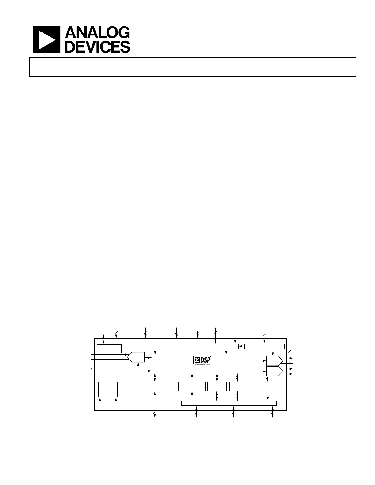
FUNCTIONAL BLOCK DIAGRAM
DIGITAL VDD DIGITAL GROUNDANALOG VDD
3.3V
3 3 3
1.8V
2-CHANNEL
ANALOG
INPUT
FILTA/
ADC_RES
Rev. A
Information furnished by Analog Devices is believed to be accurate and reliable. However, no
responsibility is assumed by Analog Devices for its use, nor for any infringements of patents or other
rights of third parties that may result from its use. Specifications subject to change without notice. No
license is granted by implication or otherwise under any patent or patent rights of Analog Devices.
Trademarks and registered trademarks are the property of their respective owners.
REGULATOR
2
RESET/
MODE
SELECT
RESET SEL F-BOOT DIGITAL IN OR GPIO AUX ADC OR GPIO DIGITAL OUT OR GP IO
STEREO
ADC
CONTROL I NTERFACE
AND SELF-BOOT
2
C/SPI AND WRITEBACK
I
ADAU1401A
AUDIO PROCESSOR CORE, 40ms DELAY MEMORY
NALO
GROUND
28-/56-BIT, 50MIPS
8-CHANNEL
DIGITAL INPUT
Figure 1.
PLL MODE
2
One Technology Way, P.O. Box 9106, Norwood, MA 02062-9106, U.S.A.
Tel: 781.329.4700 www.analog.com
Fax: 781.461.3113 ©2010 Analog Devices, Inc. All rights reserved.
PLL LOOP
FILTER
3
PLL CLOCK OS CILLATO R
8-BIT AUX
ADC
GPIO
INPUT/OUTPUT MATRIX
CRYSTAL
2
DAC
DAC
8-CHANNEL
DIGITAL OUTPUT
3335
FILTD/CM
2
4-CHANNEL
ANALOG
OUTPUT
08506-001
Page 2

ADAU1401A
TABLE OF CONTENTS
Features.............................................................................................. 1
Applications....................................................................................... 1
General Description ......................................................................... 1
Functional Block Diagram .............................................................. 1
Revision History ............................................................................... 3
Specifications..................................................................................... 4
Analog Performance .................................................................... 4
Digital Input/Output.................................................................... 5
Power.............................................................................................. 6
Temperature Range ...................................................................... 6
PLL and Oscillator........................................................................ 6
Regulator........................................................................................ 6
Digital Timing Specifications ..................................................... 7
Absolute Maximum Ratings.......................................................... 10
Thermal Resistance .................................................................... 10
ESD Caution................................................................................ 10
Pin Configuration and Function Descriptions........................... 11
Typical Performance Characteristics ........................................... 14
System Block Diagram................................................................... 15
Theory of Operation ...................................................................... 16
Initialization .................................................................................... 17
Power-Up Sequence ................................................................... 17
Control Registers Setup............................................................. 17
Recommended Program/Parameter Loading Procedure .....17
Power Reduction Modes............................................................ 17
Using the Oscillator.................................................................... 18
Setting Master Clock/PLL Mode.............................................. 18
Voltage Regulator ....................................................................... 19
Audio ADCs.................................................................................... 20
Audio DACs ....................................................................................21
Control Ports................................................................................... 22
I2C Port ........................................................................................ 23
SPI Port........................................................................................ 26
Self-Boot ...................................................................................... 27
Signal Processing ............................................................................ 29
Numeric Formats........................................................................ 29
Programming.............................................................................. 29
RAMs and Registers ....................................................................... 30
Address Maps.............................................................................. 30
Parameter RAM.......................................................................... 30
Data RAM ................................................................................... 30
Read/Write Data Formats ......................................................... 30
Control Register Map..................................................................... 32
Control Register Details ................................................................ 34
Address 2048 to Address 2055 (0x0800 to 0x0807)—Interface
Registers....................................................................................... 34
Address 2056 (0x0808)—GPIO Pin Setting Register............ 35
Address 2057 to Address 2060 (0x0809 to 0x080C)—
Auxiliary ADC Data Registers.................................................. 36
Address 2064 to Address 2068 (0x0810 to 0x0814)—Safeload
Data Registers ............................................................................. 37
Address 2069 to Address 2073 (0x0815 to 0x0819)—Safeload
Address Registers ....................................................................... 37
Address 2074 and Address 2075 (0x081A and 0x081B)—Data
Capture Registers........................................................................ 38
Address 2076 (0x081C)—DSP Core Control Register.......... 39
Address 2078 (0x081E)—Serial Output Control Register.... 40
Address 2079 (0x081F)—Serial Input Control Register ....... 41
Address 2080 and Address 2081 (0x0820 and 0x0821)—
Multipurpose Pin Configuration Registers............................. 42
Address 2082 (0x0822)—Auxiliary ADC and Power Control
Register ........................................................................................ 43
Address 2084 (0x0824)—Auxiliary ADC Enable Register ... 43
Address 2086 (0x0826)—Oscillator Power-Down Register . 43
Address 2087 (0x0827)—DAC Setup Register....................... 43
Multipurpose Pins.......................................................................... 44
Auxiliary ADC............................................................................ 44
General-Purpose Input/Output Pins....................................... 44
Serial Data Input/Output Ports ................................................ 44
Layout Recommendations............................................................. 47
Parts Placement .......................................................................... 47
Grounding................................................................................... 47
Typical Application Schematics.................................................... 48
Self-Boot Mode........................................................................... 48
I2C Control.................................................................................. 49
SPI Control.................................................................................. 50
Outline Dimensions....................................................................... 51
Ordering Guide .......................................................................... 51
Rev. A | Page 2 of 52
Page 3

ADAU1401A
REVISION HISTORY
11/10—Rev. 0 to Rev. A
Changes to Figure 7 and Table 11 .................................................11
Changes to Figure 37 ......................................................................48
Changes to Figure 38 ......................................................................49
Changes to Figure 39 ......................................................................50
4/10—Revision 0: Initial Version
Rev. A | Page 3 of 52
Page 4

ADAU1401A
SPECIFICATIONS
AVDD = 3.3 V, DVDD = 1.8 V, PVDD = 3.3 V, IOVDD = 3.3 V, master clock input = 12.288 MHz, unless otherwise noted.
ANALOG PERFORMANCE
Specifications are guaranteed at 25°C (ambient).
Table 1.
Parameter Min Typ Max Unit Test Conditions/Comments
ADC INPUTS
Number of Channels 2 Stereo input
Resolution 24 Bits
Full-Scale Input 100 (283) µA rms (µA p-p)
Signal-to-Noise Ratio
Dynamic Range −60 dB with respect to full-scale analog input
Total Harmonic Distortion + Noise −83 dB −3 dB with respect to full-scale analog input
Interchannel Gain Mismatch 25 300 mdB
Crosstalk −82 dB Analog channel-to-channel crosstalk
DC Bias 1.4 1.5 1.6 V
Gain Error −11 +11 %
DAC OUTPUTS
Number of Channels 4 Two stereo output channels
Resolution 24 Bits
Full-Scale Analog Output 0.9 (2.5) V rms (V p-p) Sine wave
Signal-to-Noise Ratio
Dynamic Range −60 dB with respect to full-scale analog output
Total Harmonic Distortion + Noise −90 dB −1 dB with respect to full-scale analog output
Crosstalk −100 dB Analog channel-to-channel crosstalk
Interchannel Gain Mismatch 25 250 mdB
Gain Error −10 +10 %
DC Bias 1.4 1.5 1.6 V
VOLTAGE REFERENCE
Absolute Voltage, CM Pin 1.4 1.5 1.6 V
AUXILIARY ADC
Full-Scale Analog Input 2.8 2.95 3.1 V
INL 0.5 LSB
DNL 0.5 LSB
Offset 15 mV
Input Impedance 17.8 30 42 kΩ
Specifications are guaranteed at 130°C (ambient).
A-Weighted 100 dB
A-Weighted 95 100 dB
A-Weighted 104 dB
A-Weighted 99 104 dB
2 V rms input with 20 kΩ (18 kΩ external + 2 kΩ internal)
series resistor
Table 2.
Parameter Min Typ Max Unit Test Conditions/Comments
ADC INPUTS
Number of Channels 2 Stereo input
Resolution 24 Bits
Full-Scale Input 100 (283) µA rms (µA p-p)
2 V rms input with 20 kΩ (18 kΩ external + 2 kΩ internal)
series resistor
Rev. A | Page 4 of 52
Page 5
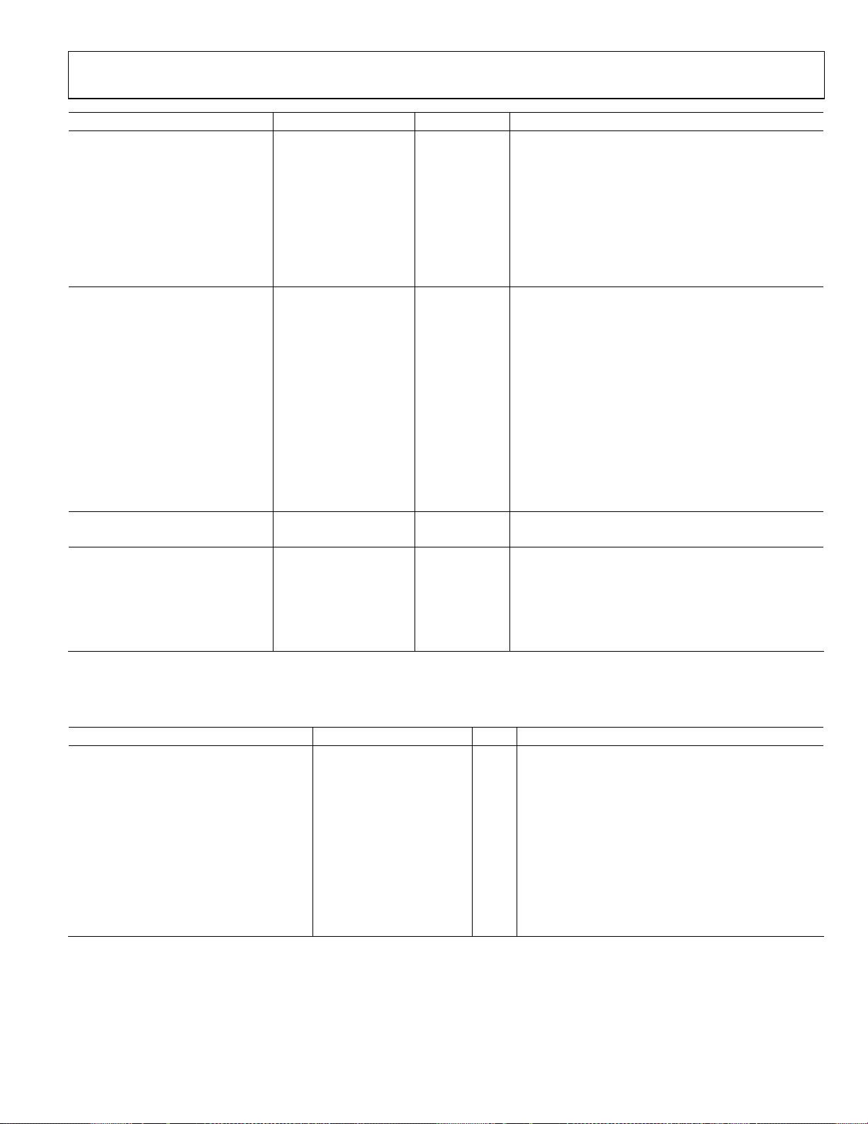
ADAU1401A
Parameter Min Typ Max Unit Test Conditions/Comments
Signal-to-Noise Ratio
A-Weighted 100 dB
Dynamic Range −60 dB with respect to full-scale analog input
A-Weighted 92 100 dB
Total Harmonic Distortion + Noise −83 dB −3 dB with respect to full-scale analog input
Interchannel Gain Mismatch 25 250 mdB
Crosstalk −82 dB Analog channel-to-channel crosstalk
DC Bias 1.4 1.5 1.6 V
Gain Error −11 +11 %
DAC OUTPUTS
Number of Channels 4 Two stereo output channels
Resolution 24 Bits
Full-Scale Analog Output 0.85 (2.4) V rms (V p-p) Sine wave
Signal-to-Noise Ratio
A-Weighted 104 dB
Dynamic Range −60 dB with respect to full-scale analog output
A-Weighted 98 104 dB
Total Harmonic Distortion + Noise −90 dB −1 dB with respect to full-scale analog output
Crosstalk −100 dB Analog channel-to-channel crosstalk
Interchannel Gain Mismatch 25 250 mdB
Gain Error −10 +10 %
DC Bias 1.4 1.5 1.6 V
VOLTAGE REFERENCE
Absolute Voltage, CM Pin 1.4 1.5 1.6 V
AUXILIARY ADC
Full-Scale Analog Input 2.8 2.95 3.1 V
INL 0.5 LSB
DNL 0.5 LSB
Offset 15 mV
Input Impedance 17.8 30 42 kΩ
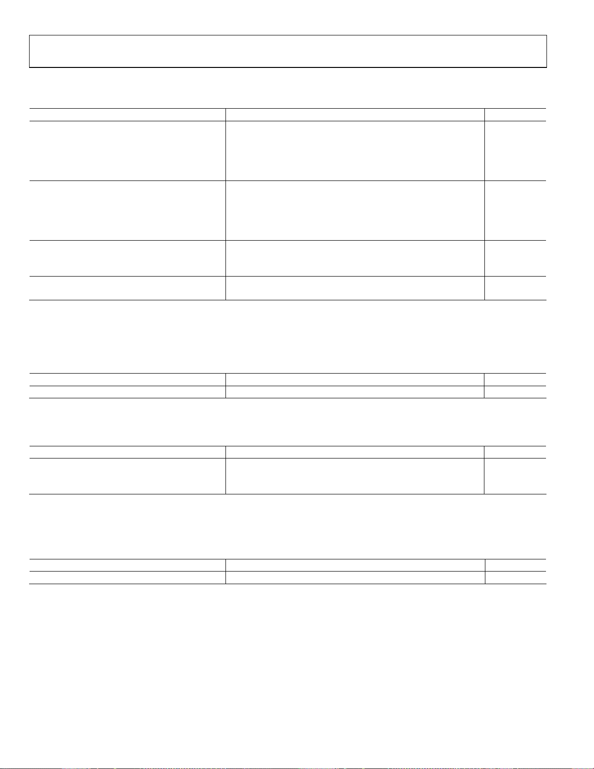
DIGITAL INPUT/OUTPUT
Table 3.
Parameter Min Typ Max1 Unit Test Conditions/Comments
Input Voltage, High (VIH) 2.0 IOVDD V
Input Voltage, Low (VIL) 0.8 V
Input Leakage, High (IIH) 1 µA Excluding MCLKI
Input Leakage, Low (IIL) 1 µA Excluding MCLKI and bidirectional pins
Bidirectional Pin Pull-Up Current, Low 150 µA
MCLKI Input Leakage, High (IIH) 3 µA
MCLKI Input Leakage, Low (IIL) 3 µA
Output Voltage, High (VOH) 2.0 V IOH = 2 mA
Output Voltage, Low (VOL) 0.8 V IOL = 2 mA
Input Capacitance 5 pF
GPIO Output Drive 2 mA
1
Maximum specifications are measured across a temperature range of −40°C to +130°C (case), a DVDD range of 1.62 V to 1.98 V, and an AVDD range of 2.97 V to 3.63 V.
Rev. A | Page 5 of 52
Page 6
ADAU1401A
POWER
Table 4.
Parameter Min Typ Max1 Unit
SUPPLY VOLTAGE
Analog Voltage 3.3 V
Digital Voltage 1.8 V
PLL Voltage 3.3 V
IOVDD Voltage 3.3 V
SUPPLY CURRENT
Analog Current (AVDD and PVDD) 50 85 mA
Digital Current (DVDD) 25 40 mA
Analog Current, Reset 35 55 mA
Digital Current, Reset 1.5 4.5 mA
DISSIPATION
Operation (AVDD, DVDD, PVDD)2 259.5 mW
Reset, All Supplies 118 mW
POWER SUPPLY REJECTION RATIO (PSRR)
1 kHz, 200 mV p-p Signal at AVDD 50 dB
1
Maximum specifications are measured across a temperature range of −40°C to +130°C (case), a DVDD range of 1.62 V to 1.98 V, and an AVDD range of 2.97 V to 3.63 V.
2
Power dissipation does not include IOVDD power because the current drawn from this supply is dependent on the loads at the digital output pins.
TEMPERATURE RANGE
Table 5.
Parameter Min Typ Max Unit
Functionality Guaranteed −40 +105 °C ambient
PLL AND OSCILLATOR
Table 6.
Parameter1 Min Typ Max Unit
PLL Operating Range MCLK_Nom − 20% MCLK_Nom + 20% MHz
PLL Lock Time 20 ms
Crystal Oscillator Transconductance (gm) 78 mmho
1
Maximum specifications are measured across a temperature range of −40°C to +130°C (case), a DVDD range of 1.62 V to 1.98 V, and an AVDD range of 2.97 V to 3.63 V.
REGULATOR
Table 7.
Parameter1 Min Typ Max Unit
DVDD Voltage 1.7 1.8 1.84 V
1
Regulator specifications are calculated using a Zetex Semiconductors FZT953 transistor in the circuit.
Rev. A | Page 6 of 52
Page 7

ADAU1401A
DIGITAL TIMING SPECIFICATIONS
Table 8.
Limit
Parameter1 t
MASTER CLOCK
tMP 36 244 ns MCLKI period, 512 × fS mode.
tMP 48 366 ns MCLKI period, 384 × fS mode.
tMP 73 488 ns MCLKI period, 256 × fS mode.
tMP 291 1953 ns MCLKI period, 64 × fS mode.
SERIAL PORT
t
40 ns INPUT_BCLK low pulse width.
BIL
t
40 ns INPUT_BCLK high pulse width.
BIH
t
10 ns INPUT_LRCLK setup; time to INPUT_BCLK rising.
LIS
t
10 ns INPUT_LRCLK hold; time from INPUT_BCLK rising.
LIH
t
10 ns SDATA_INx setup; time to INPUT_BCLK rising.
SIS
t
10 ns SDATA_INx hold; time from INPUT_BCLK rising.
SIH
t
10 ns OUTPUT_LRCLK setup in slave mode.
LOS
t
10 ns OUTPUT_LRCLK hold in slave mode.
LOH
tTS 5 ns OUTPUT_BCLK falling to OUTPUT_LRCLK timing skew.
t
40 ns SDATA_OUTx delay in slave mode; time from OUTPUT_BCLK falling.
SODS
t
40 ns SDATA_OUTx delay in master mode; time from OUTPUT_BCLK falling.
SODM
SPI PORT
f
CCLK
t
80 ns CCLK pulse width low.
CCPL
t
80 ns CCLK pulse width high.
CCPH
t
0 ns CLATCH setup; time to CCLK rising.
CLS
t
100 ns CLATCH hold; time from CCLK rising.
CLH
t
80 ns CLATCH pulse width high.
CLPH
t
0 ns CDATA setup; time to CCLK rising.
CDS
t
80 ns CDATA hold; time from CCLK rising.
CDH
t
101 ns COUT delay; time from CCLK falling.
COD
I2C PORT
f
SCL
t
0.6 µs SCL high.
SCLH
t
1.3 µs SCL low.
SCLL
t
0.6 µs SCL setup time, relevant for repeated start condition.
SCS
t
0.6 µs SCL hold time. After this period, the first clock is generated.
SCH
tDS 100 ns Data setup time.
t
300 ns SCL rise time.
SCR
t
300 ns SCL fall time.
SCF
t
300 ns SDA rise time.
SDR
t
300 ns SDA fall time.
SDF
t
0.6 Bus-free time; time between stop and start.
BFT
MULTIPURPOSE PINS AND RESET
t
50 ns GPIO rise time.
GRT
t
50 ns GPIO fall time.
GFT
t
1.5 × 1/fS µs GPIO input latency; time until high/low value is read by core.
GIL
t
20 ns
RLPW
1
All timing specifications are given for the default (I2S) states of the serial input port and the serial output port (see Table 66).
t
MIN
Unit Description
MAX
6.25 MHz CCLK frequency.
400 kHz SCL frequency.
RESET
low pulse width.
Rev. A | Page 7 of 52
Page 8
ADAU1401A
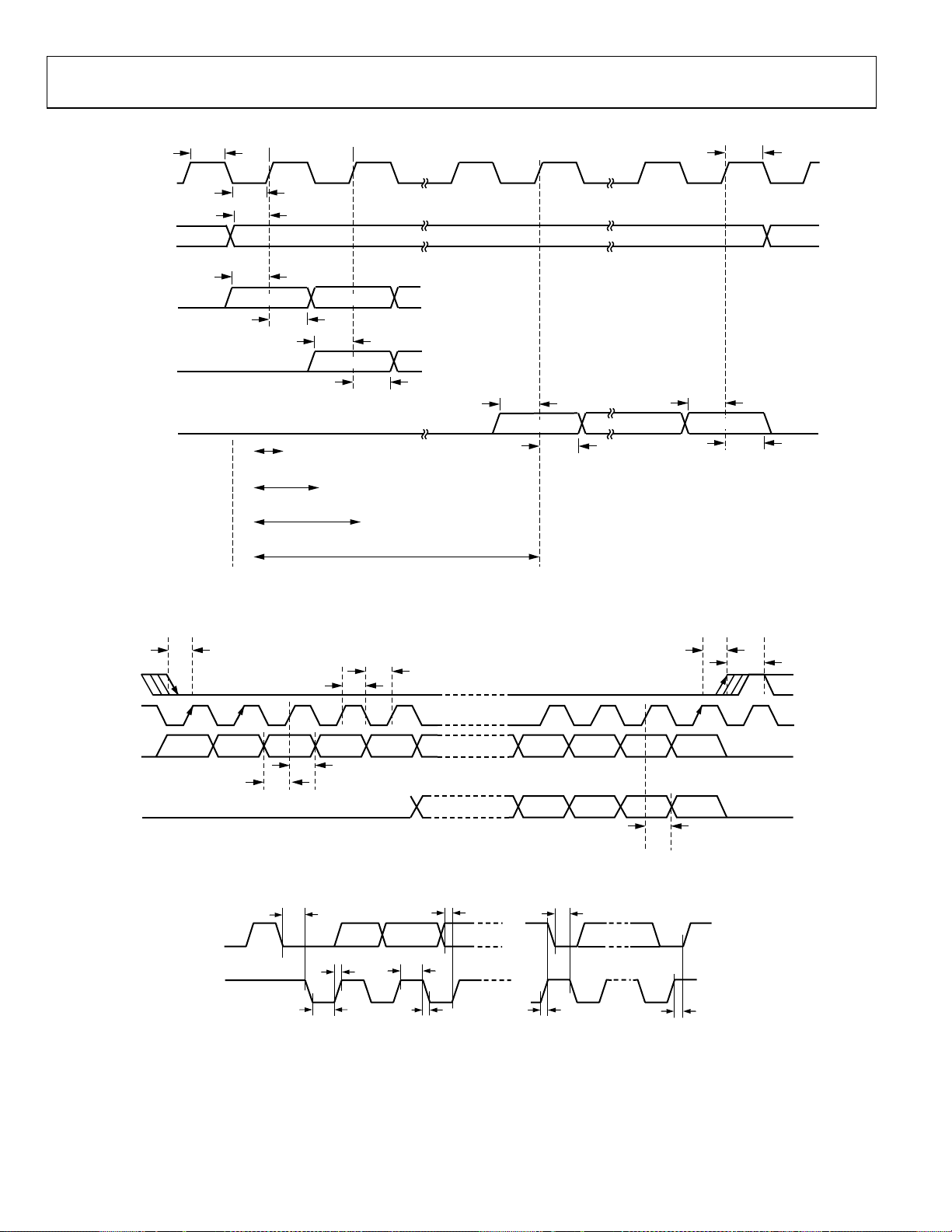
Digital Timing Diagrams
t
LIH
t
SIS
LSB
t
SIH
8506-002
t
CLPH
INPUT_BCLK
INPUT_LRCLK
SDATA_INx
LEFT-JUSTIFIED
RIGHT-JUSTIFIED
SDATA_INx
SDATA_INx
CLATCH
MODE
I2S MODE
MODE
t
BIH
t
BIL
t
LIS
t
SIS
MSB
t
SIH
8-BIT CLOCKS
(24-BIT DATA)
12-BIT CLOCKS
(20-BIT DATA)
14-BIT CLOCKS
(18-BIT DATA)
16-BIT CLOCKS
(16-BIT DATA)
MSB – 1
t
SIS
MSB
t
SIH
t
SIS
MSB
t
SIH
Figure 2. Serial Input Port Timing
t
CLS
t
t
CCPH
CCPL
t
CLH
CCLK
CDATA
t
CDH
t
COD
08506-004
COUT
t
CDS
Figure 3. SPI Port Timing
t
t
SCLH
t
SCF
Figure 4. I
DS
2
C Port Timing
t
SCH
t
SCS
t
BFT
08506-005
SDA
SCL
t
SCH
t
SCR
t
SCLL
Rev. A | Page 8 of 52
Page 9
ADAU1401A
t
TS
OUTPUT_BCLK
t
LOS
OUTPUT_L RCLK
t
SODS
t
SODM
MSB
8-BIT CLOCKS
(24-BIT DATA)
12-BIT CLO CKS
(20-BIT DATA)
14-BIT CLO CKS
(18-BIT DATA)
16-BIT CLO CKS
(16-BIT DATA)
t
MSB – 1
t
SODS
t
SODM
MSB
t
SODS
t
SODM
MSB
LSB
08506-003
Figure 5. Serial Output Port Timing
MP
SDATA_OUTx
LEFT-JUSTIFIED
RIGHT -JUSTI FIED
MODE
SDATA_OUTx
2
I
S MODE
SDATA_OUTx
MODE
MCLKI
RESET
t
RLPW
Figure 6. Master Clock and
RESET
Timing
08506-006
Rev. A | Page 9 of 52
Page 10
ADAU1401A
ABSOLUTE MAXIMUM RATINGS
Table 9.
Parameter Rating
DVDD to Ground 0 V to 2.2 V
AVDD to Ground 0 V to 4.0 V
IOVDD to Ground 0 V to 4.0 V
Digital Inputs DGND − 0.3 V, IOVDD + 0.3 V
Maximum Junction Temperature 135°C
Storage Temperature Range −65°C to +150°C
Soldering (10 sec) 300°C
Stresses above those listed under Absolute Maximum Ratings
may cause permanent damage to the device. This is a stress
rating only; functional operation of the device at these or any
other conditions above those indicated in the operational
section of this specification is not implied. Exposure to absolute
maximum rating conditions for extended periods may affect
device reliability.
THERMAL RESISTANCE
θJA is specified for the worst-case conditions, that is, a device
soldered in a circuit board for surface-mount packages.
Table 10. Thermal Resistance
Package Type θJA θ
48-Lead LQFP 72 19.5 °C/W
Unit
JC
ESD CAUTION
Rev. A | Page 10 of 52
Page 11
ADAU1401A
PIN CONFIGURATION AND FUNCTION DESCRIPTIONS
AVDD
FILTA
VOUT0
VOUT1
VOUT2
VOUT3
AGND
FILTDCMPLL_MODE1
PLL_MODE0
AGND
36
AVDD
35
PLL_LF
34
PVDD
33
PGND
32
MCLKI
31
OSCO
30
RSVD
29
MP2/SDATA_I N2/AUX_ADC1
28
MP3/SDATA_I N3/AUX_ADC2
27
MP8/SDATA_O UT2/AUX_ADC3
26
MP9/SDATA_O UT3/AUX_ADC0
25
DGND
AGND
ADC0
ADC_RES
ADC1
RESET
SELFBOOT
ADDR0
MP4/INPUT_LRCLK
MP5/INPUT_BCLK
MP1/SDATA_I N1
MP0/SDATA_I N0
DGND
48 47 46 45 44 43 42 41 40 39 38 37
1
PIN 1
INDICATOR
2
3
4
5
6
7
8
9
10
11
12
ADAU1401A
TOP VIEW
(Not to Scale)
13 14 15 16 17 18 19 20 21 22 23 24
DVDD
MP7/SDATA_OUT1
MP6/SDATA_O UT0/TDM_I N
MP11
IOVDD
VDRIVE
ADDR1/CDATA/WB
MP10/OUTPUT_LRCLK
DVDD
SCL/CCLK
SDA/COUT
CLATCH/WP
08506-007
Figure 7. 48-Lead LQFP Pin Configuration
Table 11. Pin Function Descriptions
Pin No. Mnemonic Typ e1 Description
1, 37, 42 AGND PWR
Analog Ground Pin. The AGND, DGND, and PGND pins can be tied directly together in a
common ground plane. AGND should be decoupled to an AVDD pin with a 100 nF capacitor.
2 ADC0 A_IN
Analog Audio Input 0. Full-scale 100 A rms input. The current input allows the input voltage
level to be scaled with an external resistor. An 18 kΩ resistor results in a 2 V rms full-scale input.
See the Audio ADCS section for details.
3 ADC_RES A_IN
ADC Reference Current. The full-scale current of the ADCs can be set with an external 18 kΩ
resistor connected between this pin and ground. See the Audio ADCS section for details.
4 ADC1 A_IN
Analog Audio Input 1. Full-scale 100 A rms input. The current input allows the input voltage
level to be scaled with an external resistor. An 18 kΩ resistor results in a 2 V rms full-scale input.
5
RESET
D_IN
Active Low Reset Input. Reset is triggered on a high-to-low edge, and the ADAU1401A exits
reset on a low-to-high edge. For more information about initialization, see the Power-Up
Sequence section for details.
6 SELFBOOT D_IN
Enable/Disable Self-Boot. SELFBOOT selects control port (low) or self-boot (high). Setting
this pin high initiates a self-boot operation when the ADAU1401A is brought out of a reset.
This pin can be tied directly to the control voltage or pulled up/down with a resistor. See
the Self-Boot section.
7 ADDR0 D_IN
8 MP4/INPUT_LRCLK D_IO
2
C and SPI Address 0. In combination with ADDR1, this pin allows up to four ADAU1401A
I
devices to be used on the same I
CLATCH signal. See the I
2
2
C bus or up to two ICs to be used with a common SPI
C Port section for details.
Multipurpose GPIO/Serial Input Port LRCLK. See the Multipurpose Pins section for more
details.
9 MP5/INPUT_BCLK D_IO Multipurpose GPIO/Serial Input Port BCLK. See the Multipurpose Pins section for more details.
10 MP1/SDATA_IN1 D_IO
Multipurpose GPIO/Serial Input Port Data 1. See the Multipurpose Pins section for more
details.
11 MP0/SDATA_IN0 D_IO
Multipurpose GPIO/Serial Input Port Data 0. See the Multipurpose Pins section for more
details.
12, 25 DGND PWR
Digital Ground Pin. The AGND, DGND, and PGND pins can be tied directly together in a
common ground plane. DGND should be decoupled to a DVDD pin with a 100 nF capacitor.
13, 24 DVDD PWR
1.8 V Digital Supply. The input for this pin can be supplied either externally or generated
Rev. A | Page 11 of 52
Page 12

ADAU1401A
Pin No. Mnemonic Typ e1 Description
from a 3.3 V supply with the on-board 1.8 V regulator. DVDD should be decoupled to DGND
with a 100 nF capacitor.
14 MP7/SDATA_OUT1 D_IO
15
MP6/SDATA_OUT0/
D_IO
TDM_IN
16 MP10/OUTPUT_LRCLK D_IO
17 VDRIVE A_OUT
18 IOVDD PWR
19 MP11 D_IO
20 ADDR1/CDATA/WB D_IN
21 CLATCH/WP D_IO
22 SDA/COUT D_IO
23 SCL/CCLK D_IO
26
MP9/SDATA_OUT3/
D_IO/A_IO
AUX_ADC0
27
MP8/SDATA_OUT2/
D_IO/A_IO
AUX_ADC3
28
MP3/SDATA_IN3/
D_IO/A_IO
AUX_ADC2
29
MP2/SDATA_IN2/
D_IO/A_IO
AUX_ADC1
30 RSVD Reserved. Tie this pin to ground, either directly or through a pull-down resistor.
31 OSCO D_OUT
32 MCLKI D_IN
33 PGND PWR
34 PVDD PWR
35 PLL_LF A_OUT
36, 48 AVDD PWR 3.3 V Analog Supply. This pin should be decoupled to AGND with a 100 nF capacitor.
Multipurpose GPIO/Serial Output Port Data 1. See the Multipurpose Pins section for
more details.
Multipurpose GPIO/Serial Output Port Data 0/TDM Data Input. See the Multipurpose Pins
section for more details.
Multipurpose GPIO/Serial Output Port LRCLK. See the Multipurpose Pins section for
more details.
Drive for 1.8 V Regulator. The base of the voltage regulator external PNP transistor is
driven from VDRIVE. See the Voltage Regulator section for details.
Supply for Input and Output Pins. The voltage on this pin sets the highest input voltage that
should be seen on the digital input pins. This pin is also the supply for the digital output signals
on the control port and MPx pins. IOVDD should always be set to 3.3 V. The current draw of this
pin is variable because it is dependent on the loads of the digital outputs.
Multipurpose GPIO or Serial Output Port BCLK (OUTPUT_BCLK). See the Multipurpose Pins
section for more details.
2
C Address 1/SPI Data Input/EEPROM Writeback Trigger. ADDR1 in combination with ADDR0
I
sets the I
bus (see the I
2
C address of the IC so that four ADAU1401A devices can be used on the same I2C
2
C Port section for details). For more information about the CDATA function of this
pin, see the SPI Port section. A rising (default) or falling (if set by EEPROM messages) edge
on the WB pin triggers a writeback of the interface registers to the external EEPROM. This
function can be used to save parameter data on power-down (see the Self-Boot section
for details).
SPI Latch Signal/Self-Boot EEPROM Write Protect. CLATCH must go low at the beginning of an
SPI transaction and high at the end of a transaction. Each SPI transaction can take a different
number of cycles on the CCLK pin to complete, depending on the address and read/write
bit that are sent at the beginning of the SPI transaction (see the SPI Port section for details). The
WP pin is an open-collector output when the device is in self-boot mode. The ADAU1401A
pulls WP low to enable writes to an external EEPROM. This pin should be pulled high to
3.3 V (see the Self-Boot section for details).
2
C Data/SPI Data Output. SDA is a bidirectional open collector. The line connected to SDA
I
should have a 2.2 kΩ pull-up resistor (see the I
2
C Port section for details). COUT is used for
reading back registers and memory locations. It is three-stated when an SPI read is not
active (see the SPI Port section for details).
2
C Clock/SPI Clock. SCL is always an open-collector input when in I2C control mode. In
I
self-boot mode, SCL is an open-collector output (I
should have a 2.2 kΩ pull-up resistor (see the I
2
C master). The line connected to SCL
2
C Port section for details). CCLK can either
run continuously or be gated off between SPI transactions (see the SPI Port section for details).
Multipurpose GPIO/Serial Output Port Data 3/Auxiliary ADC Input 0. See the Multipurpose
Pins section for more details.
Multipurpose GPIO/Serial Output Port Data 2/Auxiliary ADC Input 3. See the Multipurpose
Pins section for more details.
Multipurpose GPIO/Serial Input Port Data 3/Auxiliary ADC Input 2. See the Multipurpose
Pins section for more details.
Multipurpose GPIO/Serial Input Port Data 2/Auxiliary ADC Input 1. See the Multipurpose
Pins section for more details.
Crystal Oscillator Circuit Output. A 100 Ω damping resistor should be connected between
this pin and the crystal. This output should not be used to directly drive a clock to another
IC. If the crystal oscillator is not used, this pin can be left unconnected. See the Using the
Oscillator section for details.
Master Clock Input. This pin can either be connected to a 3.3 V clock signal or be the input
from the crystal oscillator circuit. See the Setting Master Clock/PLL Mode section for details.
PLL Ground Pin. The AGND, DGND, and PGND pins can be tied directly together in a
common ground plane. PGND should be decoupled to PVDD with a 100 nF capacitor.
3.3 V Power Supply for the PLL and the Auxiliary ADC Analog Section. This pin should be
decoupled to PGND with a 100 nF capacitor.
PLL Loop Filter Connection. Two capacitors and a resistor must be connected to this pin, as
shown in Figure 15. See the Setting Master Clock/PLL Mode section for more details.
Rev. A | Page 12 of 52
Page 13

ADAU1401A
Pin No. Mnemonic Typ e1 Description
38, 39
PLL_MODE0,
PLL_MODE1
40 CM A_OUT
41 FILTD A_OUT
43 VOUT3 A_OUT
44 VOUT2 A_OUT
45 VOUT1 A_OUT
46 VOUT0 A_OUT
47 FILTA A_OUT
1
PWR = power/ground, A_IN = analog input, D_IN = digital input, A_OUT = analog output, D_IO = digital input/output, D_IO/A_IO = digital input/output or analog
input/output.
D_IN
PLL Mode Setting. These pins set the output frequency of the master clock PLL. See the
Setting Master Clock/PLL Mode section for more details.
1.5 V Common-Mode Reference. A 47 F decoupling capacitor should be connected
between this pin and ground to reduce crosstalk between the ADCs and DACs. The material of
the capacitors is not critical. This pin can be used to bias external analog circuits, as long as
those circuits are not drawing current from the pin (such as when the CM pin is connected
to the noninverting input of an op amp).
DAC Filter Decoupling Pin. A 10 F capacitor should be connected between this pin and
ground. The capacitor material is not critical. The voltage on this pin is 1.5 V.
VOUT3 DAC Output. The full-scale output voltage is 0.9 V rms. This output can be used with
an active or passive output reconstruction filter. See the Audio DACS section for details.
VOUT2 DAC Output. The full-scale output voltage is 0.9 V rms. This output can be used with
an active or passive output reconstruction filter. See the Audio DACS section for details.
VOUT1 DAC Output. The full-scale output voltage is 0.9 V rms. This output can be used with
an active or passive output reconstruction filter. See the Audio DACS section for details.
VOUT0 DAC Output. The full-scale output voltage is 0.9 V rms. This output can be used with
an active or passive output reconstruction filter. See the Audio DACS section for details.
ADC Filter Decoupling Pin. A 10 F capacitor should be connected between this pin and
ground. The capacitor material is not critical. The voltage on this pin is 1.5 V.
Rev. A | Page 13 of 52
Page 14
ADAU1401A
TYPICAL PERFORMANCE CHARACTERISTICS
0.20
0.15
0.10
0.05
0
GAIN (dB)
–0.05
–0.10
–0.15
–0.20
0 2 4 6 8 10 12 14 16 18 20 22
FREQUENCY (kHz)
Figure 8. ADC Pass-Band Filter Response
f
= 48kHz
S
08506-008
0.10
0.08
0.06
0.04
0.02
0
GAIN (dB)
–0.02
–0.04
–0.06
–0.08
–0.10
0 5 10 15 20
FREQUENCY (kHz)
Figure 10. DAC Pass-Band Filter Response
f
= 48kHz
S
8506-010
10
0
–10
–20
–30
–40
–50
GAIN (dB)
–60
–70
–80
–90
–100
0 2530354020151054
FREQUENCY (kHz)
f
= 48kHz
S
5
8506-009
Figure 9. ADC Stop-Band Filter Response
10
0
–10
–20
–30
–40
–50
GAIN (dB)
–60
–70
–80
–90
–100
0 2 4 6 8 10 12 14 16 18 20
FREQUENCY (kHz)
Figure 11. DAC Stop-Band Filter Response
f
= 48kHz
S
8506-011
Rev. A | Page 14 of 52
Page 15
ADAU1401A
V
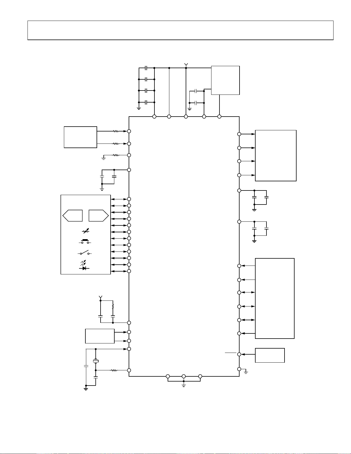
SYSTEM BLOCK DIAGRAM
100nF
3.3
AUDIO ADC
INPUT SIGNALS
10µF
MULTIPURPOSE
PIN INTERF ACES
ADCs DACs
100nF
100nF
10µF
+
IOVDD PVDD AVDD DVDD VDRIVE
18k
18k
18k
+
100nF
ADC0
ADC1
ADC_RES
FILTA
MP0
MP1
MP2
MP3
MP4
MP5
MP6
MP7
MP8
MP9
MP10
MP11
ADAU1401A
100nF
10µF
+
3.3V TO 1. 8V
REGULATOR
CIRCUIT
VOUT0
VOUT1
VOUT2
VOUT3
FILTD
CM
ADDR0
ADDR1/CDATA/WB
DAC OUTPUT FILTERS
(ACTIVE OR PASSIVE)
+
+
47µF
100nF10µ F
100nF
EEPROM,
MICROCONTRO LLER,
AND/OR SELF-BOOT
LOGIC
RESET LOGIC
08506-012
22pF
3.3V
PLL
SETTINGS
3MHz TO 25MHz
22pF
100
475
56nF3.3nF
PLL_LF
PLL_MODE0
PLL_MODE1
MCLKI
OSCO
AGND DGND PGND
CLATCH/WP
SDA/COUT
SCL/CCLK
SELFBOOT
RESET
RSVD
Figure 12. System Block Diagram
Rev. A | Page 15 of 52
Page 16

ADAU1401A
THEORY OF OPERATION
The core of the ADAU1401A is a 28-bit DSP (56-bit with doubleprecision processing) optimized for audio processing. The
program and parameter RAMs can be loaded with a custom
audio processing signal flow built using the SigmaStudio graphical
programming software from Analog Devices, Inc. The values
stored in the parameter RAM control individual signal processing
blocks, such as equalization filters, dynamics processors, audio
delays, and mixer levels. A safeload feature allows transparent
parameter updates and prevents clicks in the output signals.
The program RAM, parameter RAM, and register contents can
be saved in an external EEPROM, from which the ADAU1401A
can self-boot on startup. In this standalone mode, parameters
can be controlled through the on-board multipurpose pins. The
ADAU1401A can accept controls from switches, potentiometers,
rotary encoders, and IR receivers. Parameters such as volume
and tone settings can be saved to the EEPROM on power-down
and recalled again on power-up.
The ADAU1401A can operate with digital or analog inputs and
outputs, or a mix of both. The stereo ADC and four DACs each
have an SNR of at least +100 dB and a THD + N of at least
−83 dB. The 8-channel, flexible serial data input/output ports
allow glueless interconnection to a variety of ADCs, DACs,
general-purpose DSPs, S/PDIF receivers and transmitters, and
sample rate converters. The serial ports of the ADAU1401A can
be configured in I
2
S, left-justified, right-justified, or TDM serial
port compatible modes.
Twelve multipurpose pins (MP0 to MP11) allow the ADAU1401A
to receive external control signals as input and to output flags or
controls to other devices in the system. The MPx pins can be
configured as digital I/Os, inputs to the 4-channel auxiliary
ADC, or serial data I/O ports. As inputs, these pins can be
connected to buttons, switches, rotary encoders, potentiometers,
IR receivers, or other external circuitry to control the internal
signal processing program. When configured as outputs, these
pins can be used to drive LEDs, control other ICs, or connect to
other external circuitry in an application.
The ADAU1401A has a sophisticated control port that supports
complete read/write capability of all memory locations. Control
registers are provided to offer complete control of the configuration and serial modes of the chip. The ADAU1401A can be
configured for either SPI or I
2
C control, or it can self-boot from
an external EEPROM.
An on-board oscillator can be connected to an external crystal
to generate the master clock. In addition, a master clock phase-
locked loop (PLL) allows the ADAU1401A to be clocked from
various clock speeds. The PLL can accept inputs of 64 × f
384 × f
, or 512 × fS to generate the internal master clock of the core.
S
, 256 × fS,
S
The SigmaStudio software is used to program and control the
SigmaDSP® through the control port. Along with designing and
tuning a signal flow, SigmaStudio tools can be used to configure
all of the DSP registers and burn a new program into the external
EEPROM. The SigmaStudio graphical interface allows anyone
with digital or analog audio processing knowledge to easily design
a DSP signal flow and port it to a target application. In addition,
the interface provides enough flexibility and programmability
for an experienced DSP programmer to have in-depth control
of the design. In SigmaStudio, the user can connect graphical
blocks (such as biquad filters, dynamics processors, mixers, and
delays), compile the design, and load the program and parameter
files into the ADAU1401A memory through the control port.
Signal processing blocks available in the provided libraries include
• Single- and double-precision biquad filters
• Processors with peak or rms detection for monochannel
and multichannel dynamics
• Mixers and splitters
• Tone and noise generators
• Fixed and variable gain
• Loudness
• Delay
• Stereo enhancement
• Dynamic bass boost
• Noise and tone sources
• FIR filters
• Level detectors
• GPIO control and conditioning
Additional processing blocks are always being developed.
Analog Devices also provides proprietary and third-party
algorithms for applications such as matrix decoding, bass
enhancement, and surround virtualizers. Contact Analog
Devices for information about licensing these algorithms.
The ADAU1401A operates from a 1.8 V digital power supply
and a 3.3 V analog supply. An on-board voltage regulator can
be used to operate the chip from a single 3.3 V supply. The
ADAU1401A is fabricated on a single monolithic, integrated
circuit and is packaged in a 48-lead LQFP for operation over the
−40°C to +105°C temperature range.
Rev. A | Page 16 of 52
Page 17

ADAU1401A
INITIALIZATION
This section describes the procedure for properly setting up the
ADAU1401A. The following five-step sequence provides an
overview of how to initialize the IC:
1. Apply power to the ADAU1401A.
2. Wai t fo r t h e P L L t o l o ck .
3. Load the SigmaDSP program and parameters.
4. Set up registers (including multipurpose pins and digital
interfaces).
5. Turn off the default muting of the converters, clear the
data registers, and initialize the DAC setup register (see
the Control Registers Setup section for specific settings).
To only test analog audio pass-through (ADCs to DACs), skip
Step 3 and Step 4 and use the default internal program.
POWER-UP SEQUENCE
The ADAU1401A has a built-in power-up sequence that initializes
the contents of all internal RAMs on power-up or when the device
is brought out of a reset. On the rising edge of
of the internal program boot ROM are copied to the internal
program RAM memory, the parameter RAM is filled with values
(all 0s) from its associated boot ROM, and all registers are
initialized to 0s. The default boot ROM program copies audio
from the inputs to the outputs without processing it (see
13
). In this program, SDATA_IN0 and SDATA_IN1 are output
on DAC0 and DAC1 and on SDATA_OUT0 and
SDATA_OUT1. ADC0 and ADC1 are output on DAC2 and
DAC3. The data memories are also zeroed at power-up. New
values should not be written to the control port until the
initialization is complete.
Table 12. Power-Up Time
Maximum Program/
MCLKI Input
Frequency
3.072 MHz (64 × fS) 85 ms 175 ms 260 ms
11.2896 MHz (256 × fS) 23 ms 175 ms 198 ms
12.288 MHz (256 × fS) 21 ms 175 ms 196 ms
18.432 MHz (384 × fS) 16 ms 175 ms 191 ms
24.576 MHz (512 × fS) 11 ms 175 ms 186 ms
Init.
Time
Parame ter/Regis ter
Boot Time (I
The PLL start-up time lasts for 218 cycles of the clock on the
MCLKI pin. This time ranges from 10.7 ms for a 24.576 MHz
(512 × f
) input clock to 85.3 ms for a 3.072 MHz (64 × fS) input
S
clock and is measured from the rising edge of
the PLL startup, the duration of the ADAU1401A boot cycle is
about 42 s for a f
of 48 kHz. The user should avoid writing to or
S
reading from the ADAU1401A during this start-up time. For an
MCLKI input signal of 12.288 MHz, the full initialization sequence
(PLL startup plus boot cycle) is approximately 21 ms. As the device
comes out of a reset, the clock mode is immediately set by the
PLL_MODE0 and PLL_MODE1 pins. The reset is synchronized
to the falling edge of the internal clock.
RESET
2
C)
RESET
, the contents
Figure
To ta l
Time
. Following
Tabl e 12 lists typical times to boot the ADAU1401A into an
operational state for an application, assuming a 400 kHz I
2
C
clock loading a full program, parameter set, and all registers
(about 8.5 kB). In reality, most applications do not fill the RAMs
and, therefore, boot time is less than the value listed in Column 3
of Tab l e 1 2 .
CONTROL REGISTERS SETUP
The following registers must be set as described in this section
to initialize the ADAU1401A. These settings are the basic
minimum settings needed to operate the IC with an analog
input/output of 48 kHz. More registers may need to be set,
depending on the application. See the RAMs and Registers
section for additional settings.
DSP Core Control Register (Address 2076)
Set Bits[4:2] (ADM, DAM, and CR) each to 111.
DAC Setup Register (Address 2087)
Set Bits[1:0] (DS[1:0]) to 01.
RECOMMENDED PROGRAM/PARAMETER LOADING PROCEDURE
When writing large amounts of data to the program or parameter RAM in direct write mode, the processor core should
be disabled to prevent unpleasant noises from appearing in
the audio output. To disable the processor core,
1. Set Bits[4:3] (active low) of the DSP core control register
(Address 2076) to 1 to mute the ADCs and DACs. This
begins a volume ramp-down.
2. Set Bit 2 (active low) of the DSP core control register to 1.
This zeroes the SigmaDSP accumulators, the data output
registers, and the data input registers.
3. Fill the program RAM using burst mode writes.
4. Fill the parameter RAM using burst mode writes.
5. Set Bits[4:2] of the DSP core control register to 111.
DAC0
DAC1
DAC2
DAC3
SDATA_OUT0
08506-013
SDATA_IN0
ADC0
ADC1
Figure 13. Default Program Signal Flow
POWER REDUCTION MODES
Sections of the ADAU1401A chip can be turned on and off as
needed to reduce power consumption. These include the ADCs,
DACs, and voltage reference.
The individual analog sections can be turned off by writing to
the auxiliary ADC and power control register (Address 2082).
By default, the ADCs, DACs, and reference are enabled (all bits
Rev. A | Page 17 of 52
Page 18

ADAU1401A
V
3
F
set to 0). Each of these can be turned off by writing a 1 to the
appropriate bits in this register. The ADC power-down mode
powers down both ADCs, and each DAC can be powered down
individually. The current savings is about 15 mA when the ADCs
are powered down and about 4 mA for each DAC that is powered
down. The voltage reference, which is supplied to both the ADCs
and DACs, should only be powered down if all ADCs and DACs
are powered down. The voltage reference is powered down by
setting both Bit 6 and Bit 7 of the auxiliary ADC and power
control register.
USING THE OSCILLATOR
The ADAU1401A can use an on-board oscillator to generate its
master clock. The oscillator is designed to work with a 256 × f
master clock, which is 12.288 MHz for a f
11.2896 MHz for a f
of 44.1 kHz. The crystal in the oscillator
S
of 48 kHz and
S
circuit should be an AT-cut, parallel resonator operating at its
fundamental frequency. Figure 14 shows the external circuit
recommended for proper operation.
ADAU1401A
C1
100
OSCO
C2
Figure 14. Crystal Oscillator Circuit
MCLKI
08506-014
The 100 damping resistor on OSCO gives the oscillator a
voltage swing of approximately 2.2 V. The crystal shunt capacitance should be 7 pF. Its load capacitance should be about 18 pF,
although the circuit supports values of up to 25 pF. The necessary
values of the C1 and C2 load capacitors can be calculated from
the crystal load capacitance as follows:
C +
L
where C
×
=
C2C1
+
is the stray capacitance in the circuit and is usually
STRAY
C
STRAY
C2C1
assumed to be approximately 2 pF to 5 pF.
OSCO should not be used to drive the crystal signal directly to
another IC. This signal is an analog sine wave, and it is not appropriate to use it to drive a digital input. There are two options for
using the ADAU1401A to provide a master clock to other ICs in
the system. The first, and less recommended, method is to use a
high impedance input digital buffer on the OSCO signal. If this
approach is used, minimize the trace length to the buffer input.
The second method is to use a clock from the serial output port.
Pin 19 (MP11) can be set as an output (master) clock divided down
from the internal core clock. If this pin is set to serial output port
(OUTPUT_BCLK) mode in the multipurpose pin configuration
register (Address 2081) and the port is set to master in the serial
output control register (Address 2078), the desired output frequency can also be set in the serial output control register with
the OBF[1:0] bits (see Tab le 4 9).
S
If the oscillator is not used in the design and a system master clock
is already available in the system, the oscillator can be powered
down to save power. By default, the oscillator is powered on. The
oscillator powers down when a 1 is written to the OPD bit of
the oscillator power-down register (Address 2086; see Tabl e 60 ).
SETTING MASTER CLOCK/PLL MODE
The MCLKI input of the ADAU1401A feeds a PLL, which
generates the 50 MIPS SigmaDSP core clock. In normal operation,
the input to MCLKI must be one of the following: 64 × f
384 × f
, or 512 × fS, where fS is the input sampling rate. The mode
S
is set by configuring PLL_MODE0 and PLL_MODE1 as described
in Tabl e 1 3 . If the ADAU1401A is set to receive double-rate signals
(by reducing the number of program steps per sample by a factor
of 2 using the core control register), the master clock frequency
must be 32 × f
, 128 × fS, 192 × fS, or 256 × fS. If the ADAU1401A
S
is set to receive quad-rate signals (by reducing the number of
program steps per sample by a factor of 4 using the DSP core
control register), the master clock frequency must be 16 × f
, 96 × fS, or 128 × fS. On power-up, a clock signal must be
64 × f
S
present on the MCLKI pin so that the ADAU1401A can complete
its initialization routine.
Table 13. PLL Modes
MCLKI Input
Frequency
PLL_MODE0 PLL_MODE1
64 × fS 0 0
256 × fS 0 1
384 × f
1 0
S
512 × f
1 1
S
The clock mode should not be changed without also resetting
the ADAU1401A. If the mode is changed during operation, a
click or pop may result in the output signals. The state of the
PLL_MODEx pins should be changed while
RESET
The PLL loop filter should be connected to the PLL_LF pin. This
filter, shown in Figure 15, includes three passive components—
two capacitors and a resistor. The values of these components
do not need to be exact; the tolerance can be up to 10% for the
resistor and up to 20% for the capacitors. The 3.3 V signal shown in
Figure 15 can be connected to the AVDD supply of the chip.
3.3
475
.3n
PLL_LF
Figure 15. PLL Loop Filter
56nF
ADAU1401A
08506-015
, 256 × fS,
S
,
S
is held low.
Rev. A | Page 18 of 52
Page 19

ADAU1401A
V
VOLTAGE REGULATOR
The digital voltage of the ADAU1401A must be set to 1.8 V. The
chip includes an on-board voltage regulator that allows the
device to be used in systems without an available 1.8 V supply
but with an available 3.3 V supply. The only external components
needed in such instances are a PNP transistor, a resistor, and a
few bypass capacitors. Only one pin, VDRIVE, is necessary to
support the regulator.
The recommended design for the voltage regulator is shown
in Figure 16. The 10 µF and 100 nF capacitors shown in this
configuration are recommended for bypassing, but are not
necessary for operation. Each DVDD pin should have its own
100 nF bypass capacitor, but only one bulk capacitor (10 µF to
47 µF) is needed for both DVDD pins. With this configuration,
3.3 V is the main system voltage; 1.8 V is generated at the
transistor’s collector, which is connected to the DVDD pins.
VDRIVE is connected to the base of the PNP transistor. If the
regulator is not used in the design, VDRIVE can be tied to ground.
Two specifications must be considered when choosing a regulator transistor: the transistor’s current amplification factor
(h
or beta) should be at least 100, and the transistor’s collector
FE
must be able to dissipate the heat generated when regulating
from 3.3 V to 1.8 V. The maximum digital current drawn from
the ADAU1401A is 40 mA. The equation to determine the
minimum power dissipation of the transistor is as follows:
(3.3 V − 1.8 V) × 60 mA = 90 mW
There are many transistors with these specifications available in
small SOT-23 or SOT-223 packages.
10µF
+
100nF
DVDD
VDRIVE
Figure 16. Voltage Regulator Configuration
3.3
1k
ADAU1401A
08506-016
Rev. A | Page 19 of 52
Page 20

ADAU1401A
AUDIO ADCs
The ADAU1401A has two Σ- ADCs. The signal-to-noise ratio
(SNR) of the ADCs is 100 dB, and the THD + N is −83 dB.
The stereo audio ADCs are current input; therefore, a voltageto-current resistor is required on the inputs. This means that
the voltage level of the input signals to the system can be set to
any level; only the input resistors need to be scaled to provide
the proper full-scale current input. The ADC0 and ADC1 input
pins, as well as the ADC_RES pin, have an internal 2 kΩ resistor
for ESD protection. The voltage seen directly on the ADC input
pins is the 1.5 V common-mode voltage.
The external resistor connected to ADC_RES sets the full-scale
current input of the ADCs. The full range of the ADC inputs is
100 µA rms with an external 18 kΩ resistor on ADC_RES (20 kΩ
total, because it is in series with the internal 2 kΩ). The only
reason to change the ADC_RES resistor is if a sampling rate
other than 48 kHz is used.
The voltage-to-current resistors connected to ADC0 and ADC1 set
the full-scale voltage input of the ADCs. With a full-scale current
input of 100 µA rms, a 2.0 V rms signal with an external 18 kΩ
resistor (in series with the 2 kΩ internal resistor) results in an
input using the full range of the ADC. The matching of these
resistors to the ADC_RES resistor is important to the operation of
the ADCs. For these three resistors, a 1% tolerance is recommended.
The ADC0 input pin and/or the ADC1 input pin can be left
unconnected if the corresponding channel of the ADC is unused.
The calculations of resistor values assume a 48 kHz sample rate.
The recommended input and current setting resistors scale linearly
with the sample rate because the ADCs have a switched-capacitor
input. The total value (2 kΩ internal plus external resistor) of the
ADC_RES resistor with sample rate f
can be calculated as
S_NEW
follows:
R
TOTAL
k20 ×=
000,48
f
NEWS
_
The values of the resistors (internal plus external) in series with
the ADC0 and ADC1 pins can be calculated as follows:
TOTALINPUT
VoltageInputrmsR
k10)( ××=
000,48
f
NEWS
_
Tabl e 14 lists the external and total resistor values for common
signal input levels at a 48 kHz sampling rate. A full-scale rms
input voltage of 0.9 V is shown in the table because a full-scale
signal at this input level is equal to a full-scale output on the DACs.
Table 14. ADC Input Resistor Values
Total ADC0/ADC1
Full-Scale
RMS Input
Voltage (V)
ADC_RES
Value (kΩ)
ADC0/ADC1
Resistor
Value (kΩ)
Input Resistance
(External +
Internal) (kΩ)
0.9 18 7 9
1.0 18 8 10
2.0 18 18 20
Figure 17 shows a typical configuration of the ADC inputs for
a 2.0 V rms input signal for a f
of 48 kHz. The 47 F capacitors are
S
used to ac-couple the signals so that the inputs are biased at 1.5 V.
47µF
47µF
Figure 17. Audio ADC Input Configuration
ADAU1401A
18k
18k
18k
ADC0
ADC1
ADC_RES
08506-017
Rev. A | Page 20 of 52
Page 21

ADAU1401A
AUDIO DACs
The ADAU1401A includes four Σ- DACs. The SNR of the
DACs is 104 dB, and the THD + N is −90 dB. A full-scale
output on the DACs is 0.9 V rms (2.5 V p-p).
The DACs are in an inverting configuration. If a signal inversion
from input to output is undesirable, it can be reversed either by
using an inverting configuration for the output filter or by simply
inverting the signal in the SigmaDSP program flow.
The DAC outputs can be filtered with either an active or passive
reconstruction filter. A single-pole, passive, low-pass filter with
a 50 kHz corner frequency, as shown in Figure 18, is sufficient
to filter the DAC out-of-band noise, although an active filter may
provide better audio performance. Figure 19 shows a triple-pole,
470µF
AD8608
Figure 19. Active DAC Output Filter
DAC_OUT
4.75k4.75k
150pF
C8
+
active, low-pass filter that provides a steeper roll-off and better
stop-band attenuation than the passive filter. In this configuration,
the V+ and V− pins of the AD8606 op amp are set to VDD and
ground, respectively.
To properly initialize the DACs, the DS[1:0] bits in the DAC
setup register (Address 2087) should be set to 01.
47µF
DAC_OUT
Figure 18. Passive DAC Output Filter
47µF
604
+
3.3nF
49.9k
560
+
5.6nF
FILTER_OUT
08506-019
FILTER_OUT
08506-018
Rev. A | Page 21 of 52
Page 22

ADAU1401A
CONTROL PORTS
The ADAU1401A can operate in one of three control modes:
2
C control, SPI control, or self-boot (no external controller).
I
The ADAU1401A has both a 4-wire SPI control port and a
2
2-wire I
C bus control port. Either port can be used to set the
RAMs and registers. When the SELFBOOT pin is low at power-
2
up, the part defaults to I
C mode but can be put into SPI control
mode by pulling the CLATCH/WP pin low three times. When
the SELFBOOT pin is set high at power-up, the ADAU1401A
loads its program, parameters, and register settings from an
external EEPROM on startup.
The control port is capable of full read/write operation for all
addressable memory locations and registers. Most signal processing
parameters are controlled by writing new values to the parameter
RAM using the control port. Other functions, such as mute and
input/output mode control, are programmed by writing to the
registers.
All addresses can be accessed in a single-address mode or a
burst mode. The first byte (Byte 0) of a control port write
W
contains the 7-bit chip address plus the R/
bit. The next two
bytes (Byte 1 and Byte 2) together form the subaddress of the
memory or register location within the ADAU1401A. This
subaddress must be two bytes because the memory locations
within the ADAU1401A are directly addressable and their sizes
exceed the range of single-byte addressing. All subsequent bytes
(starting with Byte 3) contain the data, such as control port data,
program data, or parameter data. The number of bytes per word
depends on the type of data that is being written. The exact formats
for specific types of writes are shown in to . Tabl e 22 Ta bl e 31
The ADAU1401A has several mechanisms for updating signal
processing parameters in real time without causing pops or
clicks. If large blocks of data need to be downloaded, the output
of the DSP core can be halted (using the CR bit in the DSP core
control register (Address 2076)), new data can be loaded, and
then the device can be restarted. This is typically done during
the booting sequence at startup or when loading a new program
into RAM. In cases where only a few parameters need to be
changed, they can be loaded without halting the program. To
avoid unwanted side effects while loading parameters on-the-fly,
the SigmaDSP provides the safeload registers. The safeload
registers can be used to buffer a full set of parameters (for
example, the five coefficients of a biquad) and then transfer
these parameters into the active program within one audio
frame. The safeload mode uses internal logic to prevent
contention between the DSP core and the control port.
The control port pins are multifunctional, depending on the
mode in which the part is operating. Ta b le 1 5 details these
multiple functions.
Table 15. Control Port Pins and SELFBOOT Pin Functions
Pin I2C Mode SPI Mode Self-Boot
SCL/CCLK SCL—input CCLK—input SCL—output
SDA/COUT SDA—open-collector output and input COUT—output SDA—open-collector output and input
ADDR1/CDATA/WB ADDR1—input CDATA—input WB—writeback trigger
CLATCH/WP Unused input—tie to ground or IOVDD CLATCH—input WP—EEPROM write protect, open-collector output
ADDR0 ADDR0—input ADDR0—input Unused input—tie to ground or IOVDD
Rev. A | Page 22 of 52
Page 23

ADAU1401A
I2C PORT
The ADAU1401A supports a 2-wire serial (I2C-compatible)
microprocessor bus driving multiple peripherals. Two pins—
serial data (SDA) and serial clock (SCL)—carry information
between the ADAU1401A and the system I
2
In I
C mode, the ADAU1401A is always a slave on the bus,
meaning it cannot initiate a data transfer. Each slave device is
recognized by a unique address. The address byte format is
shown in Tab l e 1 6 . The ADAU1401A slave addresses are set
with the ADDR0 and ADDR1 pins. The address resides in the
2
first seven bits of the I
C write. The LSB of this byte sets either a
read or write operation. Logic Level 1 corresponds to a read
operation, and Logic Level 0 corresponds to a write operation.
Bit 5 and Bit 6 of the address are set by tying the ADDRx pins of
the ADAU1401A to Logic Level 0 or Logic Level 1. The full byte
addresses, including the pin settings and read/
are shown in . Tabl e 17
Burst mode addressing, where the subaddresses are automatically incremented at word boundaries, can be used for writing
large amounts of data to contiguous memory locations. This
increment happens automatically after a single-word write unless a
stop condition is encountered. The registers and RAMs in the
ADAU1401A range in width from one to five bytes; therefore, the
auto-increment feature knows the mapping between subaddresses
and the word length of the destination register (or memory
location). A data transfer is always terminated by a stop condition.
Both SDA and SCL should have 2.2 kΩ pull-up resistors on the
lines connected to them. The voltage on these signal lines should
not be more than IOVDD (3.3 V).
Table 16. ADAU1401A I2C Address Byte Format
Bit 0 Bit 1 Bit 2 Bit 3 Bit 4 Bit 5 Bit 6 Bit 7
0 1 1 0 1 ADDR1 ADDR0
Table 17. ADAU1401A I2C Addresses
R/
ADDR1 ADDR0
0 0 0 0x68
0 0 1 0x69
0 1 0 0x6A
0 1 1 0x6B
1 0 0 0x6C
1 0 1 0x6D
1 1 0 0x6E
1 1 1 0x6F
W
2
C master controller.
write
(R/W) bit,
R/W
Slave Address
Addressing
Initially, each device on the I2C bus is in an idle state monitoring
the SDA and SCL lines for a start condition and the proper address.
2
The I
C master initiates a data transfer by establishing a start
condition, defined by a high-to-low transition on SDA while
SCL remains high. This indicates that an address or an address
and a data stream follow. All devices on the bus respond to the
start condition and shift the next eight bits (the 7-bit address
W
plus the R/
bit) MSB first. The device that recognizes the
transmitted address responds by pulling the data line low
during the ninth clock pulse. This ninth bit is known as an
acknowledge bit. All other devices withdraw from the bus at
W
this point and return to the idle condition. The R/
bit
determines the direction of the data. A Logic 0 on the LSB of
the first byte means that the master writes information to the
peripheral, whereas a Logic 1 means that the master reads
information from the peripheral after writing the subaddress
and repeating the start address. A data transfer takes place until
a stop condition is encountered. A stop condition occurs when
SDA transitions from low to high while SCL is held high.
2
shows the timing of an I
2
C read.
of an I
C write, and shows the timing
Figure 21
Figure 20
Stop and start conditions can be detected at any stage during the
data transfer. If these conditions are asserted out of sequence
with normal read and write operations, the ADAU1401A
immediately jumps to the idle condition. During a given SCL
high period, the user should only issue one start condition, one
stop condition, or a single stop condition followed by a single
start condition. If an invalid subaddress is issued by the user,
the ADAU1401A does not issue an acknowledge and returns to
the idle condition. If the user exceeds the highest subaddress
while in auto-increment mode, one of two actions is taken. In
read mode, the ADAU1401A outputs the highest subaddress
register contents until the master device issues a no acknowledge,
indicating the end of a read. A no-acknowledge condition is
where the SDA line is not pulled low on the ninth clock pulse
on SCL. On the other hand, if the highest subaddress location is
reached while in write mode, the data for the invalid byte is not
loaded into any subaddress register, a no acknowledge is issued
by the ADAU1401A, and the part returns to the idle condition.
Rev. A | Page 23 of 52
Page 24

ADAU1401A
SCL
110
SDA
START BY
MASTER
SCL
(CONTINUED)
SDA
(CONTINUED)
SCL
SDA 0 0 011 1
START BY
MASTER
SCL
(CONTINUED)
SDA
(CONTINUED)
0
CHIP ADDRESS BYTE
CHIP ADDRESS BYTE
SUBADDRESS BYTE 2
10
FRAME 1
FRAME 3
SUBADDRESS BYTE 2
Figure 20. I
ADDR
SEL
FRAME 1
FRAME 3
ADDR
R/W
SEL
R/W
ACK BY
ADAU1401A
ACK BY
ADAU1401A
2
C Write to ADAU1401A Clocking
ACK BY
ADAU1401A
ACK BY
ADAU1401A
REPEATED
START BY MAST ER
FRAME 2
SUBADDRESS BYTE 1
FRAME 4
DATA BYTE 1
FRAME 2
SUBADDRESS BYTE 1
FRAME 4
CHIP ADDRESS BYTE
ADAU1401A
ADAU1401A
ACK BY
ADAU1401A
ADR
SEL
ACK BY
ACK BY
R/W
ACK BY
ADAU1401A
STOP BY
MASTER
08506-020
SCL
(CONTINUED)
SDA
(CONTINUED)
FRAME 5
READ DATA BYTE 1
Figure 21. I
ACK BY
MASTER
2
C Read from ADAU1401A Clocking
READ DATA BYTE 2
FRAME 6
ACK BY
MASTER
STOP BY
MASTER
08506-021
Rev. A | Page 24 of 52
Page 25

ADAU1401A
I2C Read and Write Operations
Figure 22 shows the timing of a single-word write operation. On
every ninth clock, the ADAU1401A issues an acknowledge by
pulling SDA low.
Figure 23 shows the timing of a burst mode write sequence.
This figure shows an example where the target destination
registers are two bytes. The ADAU1401A knows to increment
its subaddress register every two bytes because the requested
subaddress corresponds to a register or memory area with a
word length of two bytes.
The timing of a single-word read operation is shown in
W
Figure 24. Note that the first R/
bit is 0, indicating a write
operation. This is because the subaddress still needs to be
written to set up the internal address. After the ADAU1401A
acknowledges the receipt of the subaddress, the master must
CHIP ADDRESS,
S
R/W = 0
S = START BIT, P = STOP BIT, AS = ACKNOWLEDGE BY SLAVE.
SHOWS A ONE- WORD WRIT E, WHERE EACH WORD HAS N BYTES.
AS
SUBADDRESS,
HIGH BYTE
SUBADDRESS,
AS AS AS AS ... AS P
LOW BYTE
Figure 22. Single-Word I
CHIP
S AS AS ASASASASAS ASAS
ADDRESS,
R/W = 0
SUBADDRESS,
HIGH BYTE
SUBADDRESS,
LOW BYTE
issue a repeated start command followed by the chip address
W
byte with the R/
bit set to 1 (read). This causes the ADAU1401A
SDA to reverse and begin driving data back to the master. The
master then responds every ninth pulse with an acknowledge
pulse to the ADAU1401A.
Figure 25 shows the timing of a burst mode read sequence. This
figure shows an example where the target read registers are two
bytes. The ADAU1401A increments its subaddress register every
two bytes because the requested subaddress corresponds to a
register or memory area with word lengths of two bytes. Other
addresses may have word lengths ranging from one to five bytes.
The ADAU1401A always decodes the subaddress and sets the
auto-increment circuit so that the address increments after the
appropriate number of bytes.
DATA
BYTE 1
2
C Write Format
DATA
BYTE 2
DATA
BYTE N
08506-022
...
P
DATA-WORD 1,
BYTE 1
S = START BIT, P = STOP BIT, AS = ACKNOWLEDG E BY SLAVE.
SHOWS AN N-WORD WRITE, WHERE EACH WORD HAS TWO BYTES. (OTHER WORD LENGTHS ARE POSSIBLE, RANGING FROM ONE TO FIVE BYTES.)
Figure 23. Burst Mode I
DATA-WORD 1,
BYTE 2
2
DATA-WO RD 2,
BYTE 1
C Write Format
DATA-WORD 2,
BYTE 2
DATA-WO RD N,
BYTE 1
DATA-WO RD N,
BYTE 2
08506-023
CHIP ADDRESS,
S
R/W = 0
S = START BIT, P = STOP BIT, AM = ACKNOWLEDG E BY MASTER, AS = ACKNOWLEDGE BY SLAVE.
SHOWS A ONE- WORD READ, W HERE EACH WORD HAS N BYT ES.
SUBADDRESS,
HIGH BYTE
SUBADDRESS,
LOW BYTE
Figure 24. Single-Word I
CHIP ADDRESS,
R/W = 1
2
C Read Format
DATA
BYTE 1
DATA
BYTE 2
DATA
...
AMAMAS AMAS SASAS
BYTE N
P
08506-024
CHIP
SAS AS AS AS AMAM AMAM
ADDRESS,
R/W = 0
S = START BIT, P = STOP BIT, AM = ACKNOWLEDG E BY MASTER, AS = ACKNOWLEDGE BY SLAVE.
SHOWS AN N-WO RD READ, WHERE E ACH WORD HAS TWO BYTES. (OTHER WO RD LENGTHS ARE POSSIBLE , RANGING F ROM ONE T O FIVE BY TES.)
SUBADDRESS,
HIGH BYTE
SUBADDRESS,
LOW BYTE
Figure 25. Burst Mode I
S
CHIP
ADDRESS,
R/W = 1
DATA-WORD 1,
BYTE 1
2
C Read Format
DATA-WORD 1,
BYTE 2
...
DATA-WO RD N,
BYTE 1
DATA-WO RD N,
BYTE 2
P
08506-025
Rev. A | Page 25 of 52
Page 26

ADAU1401A
SPI PORT
By default, the ADAU1401A is in I2C mode, but it can be put into
SPI control mode by pulling CLATCH/WP low three times. The
SPI port uses a 4-wire interface, consisting of the CLATCH, CCLK,
CDATA, and COUT signals, and is always a slave port. The
CLATCH signal should go low at the beginning of a transaction
and high at the end of a transaction. The CCLK signal latches
CDATA during a low-to-high transition. COUT data is shifted
out of the ADAU1401A on the falling edge of CCLK and should
be clocked into a receiving device, such as a microcontroller, on
the CCLK rising edge. The CDATA signal carries the serial input
data, and the COUT signal is the serial output data. The COUT
signal remains three-stated until a read operation is requested.
This allows other SPI-compatible peripherals to share the same
readback line. All SPI transactions have the same basic format
shown in Tabl e 19 . A timing diagram is shown in Figure 3. All
data should be written MSB first. The ADAU1401A cannot be
taken out of SPI mode without a full reset.
Chip Address, R/W
The first byte of an SPI transaction includes the 7-bit chip address
and an R/
allows two ADAU1401A devices to share a CLATCH signal, yet
still operate independently. When ADDR0 is low, the chip address
is 0000000; when ADDR0 is high, the address is 0000001 (see
Tabl e 18
transaction is a read (Logic Level 1) or a write (Logic Level 0).
W
bit. The chip address is set by the ADDR0 pin. This
). The LSB of this first byte determines whether the SPI
Table 18. ADAU1401A SPI Address Byte Format
Bit 0 Bit 1 Bit 2 Bit 3 Bit 4 Bit 5 Bit 6 Bit 7
0 0 0 0 0 0 ADDR0
R/W
Subaddress
The 12-bit subaddress word is decoded into a location in one of
the memory areas or registers. This subaddress is the location of the
appropriate RAM location or register. The MSBs of the subaddress
are zero-padded to bring the word to a full 2-byte length.
Data Bytes
The number of data bytes varies according to the register or
memory location being accessed. During a burst mode write, an
initial subaddress is written followed by a continuous sequence
of data for consecutive memory/register locations. The detailed
data format for continuous mode operation is shown in Ta bl e
23 and Tabl e 25 in the Read/Write Data Formats section.
A sample timing diagram of a single-write SPI operation to the
parameter RAM is shown in Figure 26. A sample timing diagram
of a single-read SPI operation is shown in Figure 27. In Figure 27,
the COUT pin goes from three-state to being driven at the
beginning of Byte 3. In this example, Byte 0 to Byte 2 contain the
W
addresses and the R/
bit, and subsequent bytes carry the data.
Table 19. Generic Control Word Format
Byte 0 Byte 1 Byte 2 Byte 3 Byte 41
CHIP_ADR[6:0], R/W
1
Continues to end of data.
0000, SUBADR[11:8] SUBADR[7:0] Data Data
CLATCH
CCLK
CDATA
BYTE 0 BYTE 1 BYTE2 BYTE 3
Figure 26. SPI Write to ADAU1401A Clocking (Single-Write Mode)
CLATCH
CCLK
CDATA
COUT
BYTE 0
HIGH-Z
Figure 27. SPI Read from ADAU1401A Clocking (Single-Read Mode)
BYTE 1
BYTE 2
Rev. A | Page 26 of 52
DATA DATA
HIGH-Z
08506-027
08506-026
Page 27

ADAU1401A
SELF-BOOT
On power-up, the ADAU1401A can load a program and a set
of parameters that have been saved in an external EEPROM.
Combined with the auxiliary ADC and the multipurpose pins,
this eliminates the need for a microcontroller in the system. The
self-boot is accomplished by the ADAU1401A acting as a master
2
on the I
is set high. The ADAU1401A cannot self-boot in SPI mode.
The maximum necessary EEPROM size for program and
parameters is 9248 bytes, or just over 8.5 kB. This does not
include register settings or overhead bytes, but such factors do
not add a significant number of bytes. This much memory is
needed only if the program RAM (1024 × five bytes), parameter
RAM (1024 × four bytes), and interface registers (8 × four bytes)
are completely full. Most applications do not use the full program
and parameter RAMs, thus an 8 kB EEPROM should be sufficient.
A self-boot operation is triggered on the rising edge of
when the SELFBOOT and WP pins are set high. The ADAU1401A
reads the program, parameters, and register settings from the
EEPROM. After the ADAU1401A finishes self-booting, additional
messages can be sent to the ADAU1401A on the I
this typically is not necessary in a self-booting application. The
I
mode. The ADDRx pins have different functions when the chip
is in this mode, so the settings on them can be ignored.
The ADAU1401A does not self-boot if WP is set low. Holding
this pin low allows the EEPROM to be programmed in-circuit.
The WP pin is pulled low (it typically has a resistor pull-up) to
enable writes to the EEPROM, but this, in turn, disables the
self-boot function until the WP pin is returned high.
The ADAU1401A is a master on the I
writeback. Although it is uncommon for an application using
self-boot to also have a microcontroller connected to the control
lines, care should be taken that no other device tries to write
to the I
generates SCL at 8 × f
SCL has a duty cycle of 3/8 in accordance with the I
The ADAU1401A reads from EEPROM Chip Address 0xA1. The
LSBs of the addresses of some EEPROMs are pin configurable;
in most cases, these pins should be tied low to set this address.
C bus on startup, which occurs when the SELFBOOT pin
RESET
2
C bus, although
2
C device address is 0x68 for a write and 0x69 for a read in this
2
C bus during self-boot and
2
C bus during self-boot or writeback. The ADAU1401A
; therefore, for a fS of 48 kHz, SCL is 384 kHz.
S
2
C specification.
EEPROM Format
The EEPROM data contains a sequence of messages. Each
discrete message is one of the seven types defined in Tab l e 2 0
and consists of a sequence of one or more bytes. The first byte
identifies the message type. Bytes are written MSB first. Most
messages are block write (0x01) types, which are used for writing
to the ADAU1401A program RAM, parameter RAM, and control
registers.
The body of the message following the message type should
start with a 0x00 byte; this is the chip address. As with all other
control port transactions, following the chip address is a 2-byte
register/memory address field.
Figure 28 shows an example of what should be stored in the
EEPROM, starting with EEPROM Address 0x00. In this example,
the interface registers are first set to control port write mode
(see Line 1 of Figure 28), which is followed by 18 no-operation
(no-op) bytes (see Line 2 to Line 4 of Figure 28) so that the
interface register data appears on Page 2 of the EEPROM. Next
follows the write header, which comprises a write, length and
device address (see Line 4 of Figure 28), and then 32 bytes of
interface register data (see Line 5 to Line 8 of Figure 28). Finally,
the program RAM data, starting at ADAU1401A Address 0x04
0x00 is written (see Line 9 to Line 11 of Figure 28). In this example,
the program length is 70 words, or 350 bytes, so 332 more bytes
are included in the EEPROM but are not shown in Figure 28.
Writeback
A writeback occurs when the WB pin is triggered and data is
written to the EEPROM from the ADAU1401A. This function
is typically used to save the volume setting and other parameter
settings to the EEPROM just before power is removed from the
system. A rising edge on the WB pin triggers a writeback when
the device is in self-boot mode, unless a message to set the WB pin
to be falling-edge sensitive (0x05) is contained in the self-boot
message sequence. Only one writeback takes place unless a
message to set multiple writebacks (0x04) is contained in the
self-boot message sequence. The WP pin is pulled low when a
writeback is triggered to allow writing to the EEPROM.
The ADAU1401A can only write back the contents of the interface
registers to the EEPROM. These registers are usually set by the
DSP program, but can also be written to directly after setting Bit 6
of the DSP core control register. The parameter settings that should
be saved are configured in SigmaStudio.
Rev. A | Page 27 of 52
Page 28

ADAU1401A
The writeback function writes data from the ADAU1401A
interface registers to the second page of the self-boot EEPROM,
EEPROM Address 0x20 to EEPROM Address 0x3F. Starting at
EEPROM Address 0x1A (so that the interface register data
begins at EEPROM Address 0x20), the EEPROM should be
programmed with six bytes—the message byte (0x01), two
length bytes, the chip address (0x00), and the 2-byte subaddress
for the interface registers (0x08, 0x00). There must be a
message to the DSP core control register to enable writing to
the interface registers prior to the interface register data in the
EEPROM. This should be stored in EEPROM Address 0x00.
No-op messages (0x03) can be used between messages to
ensure that these conditions are met.
Table 20. EEPROM Message Types
Message ID Message Type Following Bytes
0x00 End None
0x01 Write
0x02 Delay
0x03 No operation executed
0x04 Set multiple writebacks
0x05 Set WB to be falling-edge sensitive
0x06 End and wait for writeback None
0x01 0x00 0x05 0x00 0x08 0x1C 0x00 0x40
WRITE LENGTH DEVICE
0x03 0x03 0x03 0x03 0x03 0x03 0x03 0x03
ADDRESS
NO-OP BYTES
The ADAU1401A writes to EEPROM Chip Address 0xA0. The
LSBs of the addresses of some EEPROMs are pin configurable; in
most cases, these pins should be tied low to set the address to 0xA0.
The maximum number of bytes that is written back from the
ADAU1401A is 35 (eight 4-byte interface registers plus three
bytes of EEPROM-addressing overhead). With SCL at 384 kHz,
the writeback operation takes approximately 73 s to complete
after being triggered. Ensure that sufficient power is available to
the system to allow enough time for a writeback to complete,
especially if the WB signal is triggered from a decreasing power
supply voltage.
Two bytes indicating the message length followed by an
appropriate number of data bytes
Two bytes for delay
None
None
None
CORE CONTROL REGISTER
ADDRESS
CORE CONTROL REGISTER
DATA
0x03 0x03 0x03 0x03 0x03 0x03 0x03 0x03
NO-OP BYTES
0x03 0x03 0x01 0x00 0x23 0x00 0x08 0x00
WRITENO-OP BYTE S
0x00 0x00 0x00 0x00 0x00 0x00 0x00 0x00
0x00 0x00 0x00 0x00 0x00 0x00 0x00 0x00
0x00 0x00 0x00 0x00 0x00 0x00 0x00 0x00
0x00 0x00 0x00 0x00 0x00 0x00 0x00 0x00
0x01 0x01 0x61 0x00 0x04 0x00 0x00 0x00
WRITE LENGTH DEVICE
0x00 0x00 0x01 0x00 0x00 0x00 0xE8 0x01
0x00 0x00 0x00 0x00 0x01 0x00 0x08 0x00
PROGRAM RAM DATA (CONTINUES FOR 332 MORE BY TES)
ADDRESS
LENGTH DEVICE
INTERFACE REG ISTER DATA
INTERFACE REG ISTER DATA
INTERFACE REG ISTER DATA
INTERFACE REG ISTER DATA
PROGRAM RAM ADDRESS P ROGRAM RAM DATA
PROGRAM RAM DATA
ADDRESS
INTERFACE REGISTER
ADDRESS
8506-039
Figure 28. EEPROM Data Example
Rev. A | Page 28 of 52
Page 29

ADAU1401A
SIGNAL PROCESSING
The ADAU1401A is designed to provide all audio signal processing
functions commonly used in stereo or multichannel playback
systems. The signal processing flow is designed using the
SigmaStudio software, which allows graphical entry and realtime control of all signal processing functions.
Many of the signal processing functions are coded using full,
56-bit, double-precision arithmetic data. The input and output
word lengths of the DSP core are 24 bits. Four extra headroom
bits are used in the processor to allow internal gains of up to
24 dB without clipping. Additional gains can be achieved by
initially scaling down the input signal in the DSP signal flow.
NUMERIC FORMATS
DSP systems commonly use a standard numeric format.
Fractional number systems are specified by an A.B format,
where A is the number of bits to the left of the decimal point
and B is the number of bits to the right of the decimal point.
The ADAU1401A uses the same numeric format for both the
parameter and data values. The format is as described in the
Numerical Format: 5.23 section.
Numerical Format: 5.23
Linear range: −16.0 to (+16.0 − 1 LSB)
Examples:
1000 0000 0000 0000 0000 0000 0000 = −16.0
1110 0000 0000 0000 0000 0000 0000 = −4.0
1111 1000 0000 0000 0000 0000 0000 = −1.0
1111 1110 0000 0000 0000 0000 0000 = −0.25
1111 1111 0011 0011 0011 0011 0011 = −0.1
1111 1111 1111 1111 1111 1111 1111 = (1 LSB below 0.0)
0000 0000 0000 0000 0000 0000 0000 = 0.0
0000 0000 1100 1100 1100 1100 1101 = 0.1
0000 0010 0000 0000 0000 0000 0000 = 0.25
0000 1000 0000 0000 0000 0000 0000 = 1.0
0010 0000 0000 0000 0000 0000 0000 = 4.0
0111 1111 1111 1111 1111 1111 1111 = (16.0 − 1 LSB).
The serial port accepts up to 24 bits on the input and is signextended to the full 28 bits of the DSP core. This allows internal
gains of up to 24 dB without internal clipping.
A digital clipper circuit is used between the output of the DSP
core and the DACs or serial port outputs (see Figure 29). This
clips the top four bits of the signal to produce a 24-bit output
with a range of 1.0 (minus 1 LSB) to −1.0. Figure 29 indicates
the maximum signal levels at each point in the data flow in both
binary and decibel levels.
4-BIT SIGN EXTENSION
DATA IN
SERIAL
PORT
1.23
(0dB)
Figure 29. Numeric Precision and Clipping Structure
1.23
(0dB)
5.23
(24dB)
SIGNAL
PROCESSING
(5.23 FORMAT)
5.23
(24dB)
DIGITAL
CLIPPER
1.23
(0dB)
PROGRAMMING
On power-up, the ADAU1401A default program passes the
unprocessed input signals to the outputs (shown in Figure 13),
but the outputs are muted by default (see the Power-Up Sequence
section). There are 1024 instruction cycles per audio sample,
resulting in about 50 MIPS being available. The SigmaDSP runs
in a stream-oriented manner, meaning that all 1024 instructions
are executed each sample period. The ADAU1401A can also be set
to accept double- or quad-speed inputs by reducing the number of
instructions per sample that are set in the DSP core control register.
The part can be easily programmed using SigmaStudio (see
Figure 30), a graphical tool provided by Analog Devices. No
knowledge of writing line-level DSP code is required. More
information about SigmaStudio can be found at www.analog.com.
Figure 30. SigmaStudio Screen Shot
8506-028
08506-029
Rev. A | Page 29 of 52
Page 30

ADAU1401A
RAMS AND REGISTERS
Table 21. RAM Map and Read/Write Modes
Memory Size Address Range Read Write Write Modes
Parameter RAM 1024 × 32 0 to 1023 (0x0000 to 0x03FF) Yes Yes Direct write,1 safeload write
Program RAM 1024 × 40 1024 to 2047 (0x0400 to 0x07FF) Yes Yes Direct write1
1
Internal registers should be cleared first to prevent clicks and pops.
ADDRESS MAPS
Tabl e 21 shows the RAM map, whereas Tab l e 3 2 shows the
ADAU1401A register map. The address space encompasses a set of
registers and two RAMs: one RAM holds the signal processing
parameters and the other RAM holds the program instructions.
The program RAM and parameter RAM are initialized on powerup from on-board boot ROMs (see the Power-Up Sequence
section).
All RAMs and registers have a default value of all 0s, except for
the program RAM, which is loaded with the default program
(see the Initialization section).
PARAMETER RAM
The parameter RAM is 32 bits wide and occupies Address 0
to Address 1023. Each parameter is padded with four 0s before
the MSB to extend the 28-bit word to a full 4-byte width. The
parameter RAM is initialized to all 0s on power-up. The data
of the parameter RAM is in twos complement, 5.23 format.
This means that the coefficients can range from +16.0 (minus
1 LSB) to −16.0, with 1.0 represented by the binary word
0000 1000 0000 0000 0000 0000 0000 or by the hexadecimal
word 0x00 0x80 0x00 0x00.
The parameter RAM can be written using one of the two
following methods: a direct read/write or a safeload write.
Direct Read/Write
The direct read/write method allows direct access to the program
RAM and parameter RAM. This mode of operation is typically
used when loading a new RAM using burst mode addressing. The
clear registers bit in the DSP core control register should be set to 0
when this mode is used to prevent clicks and pops in the outputs.
Note that this mode can be used during live program execution, but
because there is no handshaking between the core and the control
port, the parameter RAM is unavailable to the DSP core during
control writes, resulting in clicks and pops in the audio stream.
Safeload Write
Up to five safeload registers can be loaded with the parameter
RAM address and data. The data is then transferred to the
requested address when the RAM is not busy. This method can
be used for dynamic updates while live program material is
playing through the ADAU1401A. For example, a complete
update of one biquad section can occur in one audio frame
while the RAM is not busy. This method is not available for
writing to the program RAM or control registers.
DATA RAM
The ADAU1401A data RAM is used to store audio data-words
for processing. For the most part, this process is transparent to
the user. The user cannot address the RAM space, which has a
size of 2k words, directly from the control port.
Data RAM utilization should be considered when implementing
blocks that require large amounts of data RAM space, such as
delays. The SigmaDSP core processes delay times in one-sample
increments; therefore, the total pool of delay available to the user
equals 2048 multiplied by the sample period. For a f
of 48 kHz,
S
the pool of available delay is a maximum of about 43 ms. In
practice, this much data memory is not available to the user
because every block in a design uses a few data memory locations
for its processing. In most DSP programs, this does not significantly impact the total delay time. The SigmaStudio compiler
manages the data RAM and indicates if the number of addresses
needed in the design exceeds the maximum number available.
READ/WRITE DATA FORMATS
The read/write formats of the control port are designed to be
byte oriented. This allows easy programming of common microcontroller chips. To fit into a byte-oriented format, 0s are appended
to the data fields before the MSB to extend the data-word to
eight bits. For example, 28-bit words written to the parameter
RAM are appended with four leading 0s to equal 32 bits (four
bytes), whereas 40-bit words written to the program RAM are
not appended with 0s because they are already a full five bytes.
These zero-padded data fields are appended to a 3-byte field
consisting of a 7-bit chip address, a read/write bit, and an 11-bit
RAM/register address. The control port knows how many data
bytes to expect based on the address given in the first three bytes.
The total number of bytes for a single-location write command can
vary from four bytes (for a control register write) to eight bytes (for
a program RAM write). Burst mode can be used to fill contiguous
register or RAM locations. A burst mode write begins by writing
the address and data of the first RAM or register location to be
written. Rather than ending the control port transaction (by issuing
a stop command in I
high in SPI mode after the data-word), as would be done in a
single-address write, the next data-word can be immediately
written without specifying its address. The ADAU1401A control
port auto-increments the address of each write, even across the
boundaries of different RAMs and registers. Tabl e 23 and Tabl e 25
show examples of burst mode writes.
2
C mode or by bringing the CLATCH signal
Rev. A | Page 30 of 52
Page 31

ADAU1401A
Table 22. Parameter RAM Read/Write Format (Single Address)
Byte 0 Byte 1 Byte 2 Byte 3 Bytes[4:6]
CHIP_ADR[6:0], W/R
Table 23. Parameter RAM Block Read/Write Format (Burst Mode)
Byte 0 Byte 1 Byte 2 Byte 3 Bytes[4:6] Bytes[7:10] Bytes[11:14]
CHIP_ADR[6:0], W/R
<—PARAM_ADR—> PARAM_ADR + 1 PARAM_ADR + 2
000000, PARAM_ADR[9:8] PARAM_ADR[7:0] 0000, PARAM[27:24] PARAM[23:0] … …
Table 24. Program RAM Read/Write Format (Single Address)
Byte 0 Byte 1 Byte 2 Bytes[3:7]
CHIP_ADR[6:0], W/R
Table 25. Program RAM Block Read/Write Format (Burst Mode)
Byte 0 Byte 1 Byte 2 Bytes[3:7] Bytes[8:12] Bytes[13:17]
CHIP_ADR[6:0], W/R
00000, PROG_ADR[10:8] PROG_ADR[7:0] PROG[39:0] … …
<—PROG_ADR—> PROG_ADR + 1 PROG_ADR + 2
000000, PARAM_ADR[9:8] PARAM_ADR[7:0] 0000, PARAM[27:24] PARAM[23:0]
00000, PROG_ADR[10:8] PROG_ADR[7:0] PROG[39:0]
Table 26. Control Register Read/Write Format (Core, Serial Out 0, Serial Out 1)
Byte 0 Byte 1 Byte 2 Byte 3 Byte 4
CHIP_ADR[6:0], W/R
0000, REG_ADR[11:8] REG_ADR[7:0] Data[15:8] Data[7:0]
Table 27. Control Register Read/Write Format (RAM Configuration, Serial Input)
Byte 0 Byte 1 Byte 2 Byte 3
CHIP_ADR[6:0], W/R
0000, REG_ADR[11:8] REG_ADR[7:0] Data[7:0]
Table 28. Data Capture Register Write Format
Byte 0 Byte 1 Byte 2 Byte 3 Byte 4
CHIP_ADR[6:0],
W
/R
1
PROGCOUNT[10:0] is the value of the program counter when the data capture occurs (the table of values is generated by the SigmaStudio compiler).
2
REGSEL[1:0] selects one of four registers (see the Address 2074 and Address 2075 (0X081A and 0X081B)—Data Capture Registers section).
0000, DATA_CAPTURE_ADR[11:8] DATA_CAPTURE_ADR[7:0] 000, PROGCOUNT[10:6]
1
PROGCOUNT[5:0],
1
REGSEL[1:0]2
Table 29. Data Capture (Control Port Readback) Register Read Format
Byte 0 Byte 1 Byte 2 Bytes[3:5]
CHIP_ADR[6:0], W/R
0000, DATA_CAPTURE_ADR[11:8] DATA_CAPTURE_ADR[7:0] Data[23:0]
Table 30. Safeload Address Register Write Format
Byte 0 Byte 1 Byte 2 Byte 3 Byte 4
CHIP_ADR[6:0], W/R
0000, SAFELOAD_ADR[11:8] SAFELOAD_ADR[7:0] 000000, PARAM_ADR[9:8] PARAM_ADR[7:0]
Table 31. Safeload Data Register Write Format
Byte 0 Byte 1 Byte 2 Byte 3 Byte 4 Bytes[5:7]
CHIP_ADR[6:0], W/R
0000, SAFELOAD_ADR[11:8] SAFELOAD_ADR[7:0] 00000000 0000, Data[27:24] Data[23:0]
Rev. A | Page 31 of 52
Page 32

ADAU1401A
CONTROL REGISTER MAP
Blank cells within Tab l e 3 2 indicate that control bits do not exist in the corresponding locations.
Table 32. Register Map
Register
Address
Hex Dec
0x0800 2048 4 Interface 0[31:16] 0 0 0 0 IF27 IF26 IF25 IF24 IF23 IF22 IF21 IF20 IF19 IF18 IF17 IF16 0x0000
Interface 0[15:0] IF15 IF14 IF13 IF12 IF11 IF10 IF09 IF08 IF07 IF06 IF05 IF04 IF03 IF02 IF01 IF00 0x0000
0x0801 2049 4 Interface 1[31:16] 0 0 0 0 IF27 IF26 IF25 IF24 IF23 IF22 IF21 IF20 IF19 IF18 IF17 IF16 0x0000
Interface 1[15:0] IF15 IF14 IF13 IF12 IF11 IF10 IF09 IF08 IF07 IF06 IF05 IF04 IF03 IF02 IF01 IF00 0x0000
0x0802 2050 4 Interface 2[31:16] 0 0 0 0 IF27 IF26 IF25 IF24 IF23 IF22 IF21 IF20 IF19 IF18 IF17 IF16 0x0000
Interface 2[15:0] IF15 IF14 IF13 IF12 IF11 IF10 IF09 IF08 IF07 IF06 IF05 IF04 IF03 IF02 IF01 IF00 0x0000
0x0803 2051 4 Interface 3[31:16] 0 0 0 0 IF27 IF26 IF25 IF24 IF23 IF22 IF21 IF20 IF19 IF18 IF17 IF16 0x0000
Interface 3[15:0] IF15 IF14 IF13 IF12 IF11 IF10 IF09 IF08 IF07 IF06 IF05 IF04 IF03 IF02 IF01 IF00 0x0000
0x0804 2052 4 Interface 4[31:16] 0 0 0 0 IF27 IF26 IF25 IF24 IF23 IF22 IF21 IF20 IF19 IF18 IF17 IF16 0x0000
Interface 4[15:0] IF15 IF14 IF13 IF12 IF11 IF10 IF09 IF08 IF07 IF06 IF05 IF04 IF03 IF02 IF01 IF00 0x0000
0x0805 2053 4 Interface 5[31:16] 0 0 0 0 IF27 IF26 IF25 IF24 IF23 IF22 IF21 IF20 IF19 IF18 IF17 IF16 0x0000
Interface 5[15:0] IF15 IF14 IF13 IF12 IF11 IF10 IF09 IF08 IF07 IF06 IF05 IF04 IF03 IF02 IF01 IF00 0x0000
0x0806 2054 4 Interface 6[31:16] 0 0 0 0 IF27 IF26 IF25 IF24 IF23 IF22 IF21 IF20 IF19 IF18 IF17 IF16 0x0000
Interface 6[15:0] IF15 IF14 IF13 IF12 IF11 IF10 IF09 IF08 IF07 IF06 IF05 IF04 IF03 IF02 IF01 IF00 0x0000
0x0807 2055 4 Interface 7[31:16] 0 0 0 0 IF27 IF26 IF25 IF24 IF23 IF22 IF21 IF20 IF19 IF18 IF17 IF16 0x0000
Interface 7[15:0] IF15 IF14 IF13 IF12 IF11 IF10 IF09 IF08 IF07 IF06 IF05 IF04 IF03 IF02 IF01 IF00 0x0000
0x0808 2056 2 GPIO pin setting 0 0 0 0 MP11 MP10 MP09 MP08 MP07 MP06 MP05 MP04 MP03 MP02 MP01 MP00 0x0000
0x0809 2057 2 Auxiliary ADC Data 0 0 0 0 0 AA11 AA10 AA09 AA08 AA07 AA06 AA05 AA04 AA03 AA02 AA01 AA00 0x0000
0x080A 2058 2 Auxiliary ADC Data 1 0 0 0 0 AA11 AA10 AA09 AA08 AA07 AA06 AA05 AA04 AA03 AA02 AA01 AA00 0x0000
0x080B 2059 2 Auxiliary ADC Data 2 0 0 0 0 AA11 AA10 AA09 AA08 AA07 AA06 AA05 AA04 AA03 AA02 AA01 AA00 0x0000
0x080C 2060 2 Auxiliary ADC Data 3 0 0 0 0 AA11 AA10 AA09 AA08 AA07 AA06 AA05 AA04 AA03 AA02 AA01 AA00 0x0000
0x080D 2061 5 Reserved[39:32] RSVD RSVD RSVD RSVD RSVD RSVD RSVD RSVD 0x00
Reserved[31:16] RSVD RSVD RSVD RSVD RSVD RSVD RSVD RSVD RSVD RSVD RSVD RSVD RSVD RSVD RSVD RSVD 0x0000
Reserved[15:0] RSVD RSVD RSVD RSVD RSVD RSVD RSVD RSVD RSVD RSVD RSVD RSVD RSVD RSVD RSVD RSVD 0x0000
0x080E 2062 5 Reserved[39:32] RSVD RSVD RSVD RSVD RSVD RSVD RSVD RSVD 0x00
Reserved[31:16] RSVD RSVD RSVD RSVD RSVD RSVD RSVD RSVD RSVD RSVD RSVD RSVD RSVD RSVD RSVD RSVD 0x0000
Reserved[15:0] RSVD RSVD RSVD RSVD RSVD RSVD RSVD RSVD RSVD RSVD RSVD RSVD RSVD RSVD RSVD RSVD 0x0000
0x080F 2063 5 Reserved[39:32] RSVD RSVD RSVD RSVD RSVD RSVD RSVD RSVD 0x00
Reserved[31:16] RSVD RSVD RSVD RSVD RSVD RSVD RSVD RSVD RSVD RSVD RSVD RSVD RSVD RSVD RSVD RSVD 0x0000
Reserved[15:0] RSVD RSVD RSVD RSVD RSVD RSVD RSVD RSVD RSVD RSVD RSVD RSVD RSVD RSVD RSVD RSVD 0x0000
0x0810 2064 5 Safeload Data 0[39:32] SD39 SD38 SD37 SD36 SD35 SD34 SD33 SD32 0x00
Safeload Data 0[31:16] SD31 SD30 SD29 SD28 SD27 SD26 SD25 SD24 SD23 SD22 SD21 SD20 SD19 SD18 SD17 SD16 0x0000
Safeload Data 0[15:0] SD15 SD14 SD13 SD12 SD11 SD10 SD09 SD08 SD07 SD06 SD05 SD04 SD03 SD02 SD01 SD00 0x0000
0x0811 2065 5 Safeload Data 1[39:32] SD39 SD38 SD37 SD36 SD35 SD34 SD33 SD32 0x00
Safeload Data 1[31:16] SD31 SD30 SD29 SD28 SD27 SD26 SD25 SD24 SD23 SD22 SD21 SD20 SD19 SD18 SD17 SD16 0x0000
Safeload Data 1[15:0] SD15 SD14 SD13 SD12 SD11 SD10 SD09 SD08 SD07 SD06 SD05 SD04 SD03 SD02 SD01 SD00 0x0000
0x0812 2066 5 Safeload Data 2[39:32] SD39 SD38 SD37 SD36 SD35 SD34 SD33 SD32 0x00
Safeload Data 2[31:16] SD31 SD30 SD29 SD28 SD27 SD26 SD25 SD24 SD23 SD22 SD21 SD20 SD19 SD18 SD17 SD16 0x0000
Safeload Data 2[15:0] SD15 SD14 SD13 SD12 SD11 SD10 SD09 SD08 SD07 SD06 SD05 SD04 SD03 SD02 SD01 SD00 0x0000
0x0813 2067 5 Safeload Data 3[39:32] SD39 SD38 SD37 SD36 SD35 SD34 SD33 SD32 0x00
Safeload Data 3[31:16] SD31 SD30 SD29 SD28 SD27 SD26 SD25 SD24 SD23 SD22 SD21 SD20 SD19 SD18 SD17 SD16 0x0000
Safeload Data 3[15:0] SD15 SD14 SD13 SD12 SD11 SD10 SD09 SD08 SD07 SD06 SD05 SD04 SD03 SD02 SD01 SD00 0x0000
0x0814 2068 5 Safeload Data 4[39:32] SD39 SD38 SD37 SD36 SD35 SD34 SD33 SD32 0x00
Safeload Data 4[31:16] SD31 SD30 SD29 SD28 SD27 SD26 SD25 SD24 SD23 SD22 SD21 SD20 SD19 SD18 SD17 SD16 0x0000
Safeload Data 4[15:0] SD15 SD14 SD13 SD12 SD11 SD10 SD09 SD08 SD07 SD06 SD05 SD04 SD03 SD02 SD01 SD00 0x0000
0x0815 2069 2 Safeload Address 0 0 0 0 0 SA11 SA10 SA09 SA08 SA07 SA06 SA05 SA04 SA03 SA02 SA01 SA00 0x0000
0x0816 2070 2 Safeload Address 1 0 0 0 0 SA11 SA10 SA09 SA08 SA07 SA06 SA05 SA04 SA03 SA02 SA01 SA00 0x0000
0x0817 2071 2 Safeload Address 2 0 0 0 0 SA11 SA10 SA09 SA08 SA07 SA06 SA05 SA04 SA03 SA02 SA01 SA00 0x0000
0x0818 2072 2 Safeload Address 3 0 0 0 0 SA11 SA10 SA09 SA08 SA07 SA06 SA05 SA04 SA03 SA02 SA01 SA00 0x0000
0x0819 2073 2 Safeload Address 4 0 0 0 0 SA11 SA10 SA09 SA08 SA07 SA06 SA05 SA04 SA03 SA02 SA01 SA00 0x0000
0x081A 2074 2 Data Capture 0 0 0 0 0 PC09 PC08 PC07 PC06 PC05 PC04 PC03 PC02 PC01 PC00 RS01 RS00 0x0000
0x081B 2075 2 Data Capture 1 0 0 0 0 PC09 PC08 PC07 PC06 PC05 PC04 PC03 PC02 PC01 PC00 RS01 RS00 0x0000
No.
of
Byte
s
Name
MSB LSB
D39 D38 D37 D36 D35 D34 D33 D32
D31 D30 D29 D28 D27 D26 D25 D24 D23 D22 D21 D20 D19 D18 D17 D16
D15 D14 D13 D12 D11 D10 D9 D8 D7 D6 D5 D4 D3 D2 D1 D0 Default
Rev. A | Page 32 of 52
Page 33

ADAU1401A
Register
Address
Hex Dec
0x081C 2076 2 DSP core control RSVD RSVD GD1 GD0 RSVD RSVD RSVD AACW GPCW IFCW IST ADM DAM CR SR1 SR0 0x0000
0x081D 2077 1 Reserved RSVD RSVD RSVD RSVD RSVD RSVD RSVD RSVD 0x00
0x081E 2078 2 Serial output control 0 0 OLRP OBP M/S OBF1 OBF0 OLF1 OLF0 FST TDM MSB2 MSB1 MSB0 OWL1 OWL0 0x0000
0x081F 2079 1 Serial input control 0 0 0 ILP IBP M2 M1 M0 0x00
0x0820 2080 3 MP Pin Config. 0[23:16] MP53 MP52 MP51 MP50 MP43 MP42 MP41 MP40 0x00
MP Pin Config. 0[15:0] MP33 MP32 MP31 MP30 MP23 MP22 MP21 MP20 MP13 MP12 MP11 MP10 MP03 MP02 MP01 MP00 0x0000
0x0821 2081 3 MP Pin Config. 1[23:16] MP113 MP112 MP111 MP110 MP103 MP102 MP101 MP100 0x00
MP Pin Config. 1[15:0] MP93 MP92 MP91 MP90 MP83 MP82 MP81 MP80 MP73 MP72 MP71 MP70 MP63 MP62 MP61 MP60 0x0000
0x0822 2082 2
0x0823 2083 2 Reserved RSVD RSVD RSVD RSVD RSVD RSVD RSVD RSVD RSVD RSVD RSVD RSVD RSVD RSVD RSVD RSVD 0x0000
0x0824 2084 2 Auxiliary ADC enable AAEN RSVD RSVD RSVD RSVD RSVD RSVD RSVD RSVD RSVD RSVD RSVD RSVD RSVD RSVD RSVD 0x0000
0x0825 2085 2 Reserved RSVD RSVD RSVD RSVD RSVD RSVD RSVD RSVD RSVD RSVD RSVD RSVD RSVD RSVD RSVD RSVD 0x0000
0x0826 2086 2 Oscillator power-down RSVD RSVD RSVD RSVD RSVD RSVD RSVD RSVD RSVD RSVD RSVD RSVD RSVD OPD RSVD RSVD 0x0000
0x0827 2087 2 DAC setup RSVD RSVD RSVD RSVD RSVD RSVD RSVD RSVD RSVD RSVD RSVD RSVD RSVD RSVD DS1 DS0 0x0000
No.
of
Byte
Name
s
Auxiliary ADC and power
control
MSB LSB
D39 D38 D37 D36 D35 D34 D33 D32
D31 D30 D29 D28 D27 D26 D25 D24 D23 D22 D21 D20 D19 D18 D17 D16
D15 D14 D13 D12 D11 D10 D9 D8 D7 D6 D5 D4 D3 D2 D1 D0 Default
RSVD RSVD RSVD RSVD RSVD RSVD FIL1 FIL0 AAPD VBPD VRPD RSVD D0PD D1PD D2PD D3PD 0x0000
Rev. A | Page 33 of 52
Page 34

ADAU1401A
CONTROL REGISTER DETAILS
ADDRESS 2048 TO ADDRESS 2055 (0x0800 TO 0x0807)—INTERFACE REGISTERS
The interface registers are used in self-boot mode to save
parameters that need to be written to the external EEPROM.
The ADAU1401A then recalls these parameters from the
EEPROM after the next reset or power-up. Therefore, system
parameters such as volume and EQ settings can be saved during
power-down and recalled the next time the system is turned on.
There are eight 32-bit interface registers, which allow eight 28-bit
(plus zero-padding) parameters to be saved. The parameters to
Table 33. Interface Registers Bit Map
D31 D30 D29 D28 D27 D26 D25 D24 D23 D22 D21 D20 D19 D18 D17 D16
D15 D14 D13 D12 D11 D10 D9 D8 D7 D6 D5 D4 D3 D2 D1 D0 Default
0 0 0 0 IF27 IF26 IF25 IF24 IF23 IF22 IF21 IF20 IF19 IF18 IF17 IF16 0x0000
IF15 IF14 IF13 IF12 IF11 IF10 IF09 IF08 IF07 IF06 IF05 IF04 IF03 IF02 IF01 IF00 0x0000
Table 34. Interface Registers Bit Descriptions
Bit Name Description
IF[27:0] Interface register 28-bit parameter
be saved in these registers are selected in the graphical
programming tools. These registers are updated with their
corresponding parameter RAM data once per sample period.
An edge, which can be set to be either rising or falling, triggers
the ADAU1401A to write the current contents of the interface
registers to the EEPROM. See the Self-Boot section for details.
The user can write directly to the interface registers after the
interface registers control port write mode bit (IFCW) in the DSP
core control register has been set. In this mode, the data in the
registers is written from the control port, not from the DSP core.
Rev. A | Page 34 of 52
Page 35

ADAU1401A
ADDRESS 2056 (0x0808)—GPIO PIN SETTING REGISTER
This register allows the user to set the GPIO pins through the
control port. High or low settings can be directly written to or
Table 35. GPIO Pin Setting Register Bit Map
D15 D14 D13 D12 D11 D10 D9 D8 D7 D6 D5 D4 D3 D2 D1 D0 Default
0 0 0 0 MP11 MP10 MP09 MP08 MP07 MP06 MP05 MP04 MP03 MP02 MP01 MP00 0x0000
Table 36. GPIO Pin Setting Register Bit Descriptions
Bit Name Description
MP[11:0] Setting of the corresponding multipurpose pin when controlled through SPI or I2C
read from this register after setting the GPIO pin setting register
control port write mode bit (GPCW) in the DSP core control
register. This register is updated once every LRCLK frame (1/f
S
).
Rev. A | Page 35 of 52
Page 36

ADAU1401A
ADDRESS 2057 TO ADDRESS 2060 (0x0809 TO 0x080C)—AUXILIARY ADC DATA REGISTERS
These registers hold the data generated by the 4-channel
auxiliary ADC. The ADCs have eight bits of precision and can
be extended to 12 bits if filtering is selected via Bits FIL[1:0] of
the auxiliary ADC and power control register. The SigmaDSP
program reads this data as a 1.11 format data-word with a range
Table 37. Auxiliary ADC Data Registers Bit Map
D15 D14 D13 D12 D11 D10 D9 D8 D7 D6 D5 D4 D3 D2 D1 D0 Default
0 0 0 0 AA11 AA10 AA09 AA08 AA07 AA06 AA05 AA04 AA03 AA02 AA01 AA00 0x0000
Table 38. Auxiliary ADC Data Registers Bit Descriptions
Bit Name Description
AA[11:0] Auxiliary ADC output data, MSB first
of 0 to 1.0. This data-word is mapped to the 5.23 format
parameter word with the four MSBs and 12 LSBs set to 0. A
full-scale code of 255 results in a value of 1.0. These registers
can be written to directly if the auxiliary ADC data registers
control port write mode bit (AACW) is set in the DSP core
control register.
Rev. A | Page 36 of 52
Page 37

ADAU1401A
ADDRESS 2064 TO ADDRESS 2068 (0x0810 TO 0x0814)—SAFELOAD DATA REGISTERS
Many applications require real-time microcontroller control of
signal processing parameters, such as filter coefficients, mixer gains,
multichannel virtualizing parameters, or dynamics processing
curves. When controlling a biquad filter, for example, all of the
parameters must be updated at the same time. Doing so prevents
the filter from executing with a mix of old and new coefficients
for one or two audio frames, thus avoiding temporary instability
and transients that may take a long time to decay. To accomplish
this, the ADAU1401A uses safeload data registers to simultaneously
load a set of five 28-bit values to the desired parameter RAM
address. Five registers are used because a biquad filter uses five
coefficients and, as previously mentioned, it is desirable to do a
complete update in one transaction.
The first step in performing a safeload operation is writing
the parameter address to one of the safeload address registers
(Address 2069 to Address 2073). The 10-bit data-word to be
written is the address in parameter RAM to which the safeload
is being performed. After this address is written, the 28-bit dataword can be written to the corresponding safeload data register
(Address 2064 to Address 2068).
The data formats for these writes are detailed in Tabl e 30 and
Tabl e 31 . Tabl e 3 9 outlines how each of the five address registers
maps to its corresponding data register.
After the address and data registers are loaded, set the initiate
safeload transfer bit in the DSP core control register to initiate
the loading into RAM. Each of the five safeload registers takes
one of the 1024 core instructions to load into the parameter
RAM. The total program lengths should, therefore, be limited
to 1019 cycles (1024 minus 5) to ensure that the SigmaDSP core
always has at least five cycles available. The safeload is guaranteed
to occur within one LRCLK period (21 µs for a f
of 48 kHz) of
S
the initiate safeload transfer bit being set.
The safeload logic automatically sends data to be loaded into
RAM from only those safeload registers that have been written
to since the last safeload operation. For example, if two parameters
are to be updated in the RAM, only two of the five safeload registers
must be written. When the initiate safeload transfer bit is asserted,
only data from those two registers are sent to the RAM; the other
three registers are not sent to the RAM and may hold old or
invalid data.
Table 39. Safeload Address and Data Register Mapping
Safeload
Register
Safeload Data 0 2069 2064
Safeload Data 1 2070 2065
Safeload Data 2 2071 2066
Safeload Data 3 2072 2067
Safeload Data 4 2073 2068
Safeload
Address Register
Safeload
Data Register
Table 40. Safeload Data Registers Bit Map
D39 D38 D37 D36 D35 D34 D33 D32
D31 D30 D29 D28 D27 D26 D25 D24 D23 D22 D21 D20 D19 D18 D17 D16
D15 D14 D13 D12 D11 D10 D9 D8 D7 D6 D5 D4 D3 D2 D1 D0 Default
SD39 SD38 SD37 SD36 SD35 SD34 SD33 SD32 0x00
SD31 SD30 SD29 SD28 SD27 SD26 SD25 SD24 SD23 SD22 SD21 SD20 SD19 SD18 SD17 SD16 0x0000
SD15 SD14 SD13 SD12 SD11 SD10 SD09 SD08 SD07 SD06 SD05 SD04 SD03 SD02 SD01 SD00 0x0000
Table 41. Safeload Data Registers Bit Descriptions
Bit Name Description
SD[39:0]
Safeload data. Data (program, parameters, register contents) to be loaded into the RAMs or
registers.
ADDRESS 2069 TO ADDRESS 2073 (0x0815 TO 0x0819)—SAFELOAD ADDRESS REGISTERS
Table 42. Safeload Address Registers Bit Map
D15 D14 D13 D12 D11 D10 D9 D8 D7 D6 D5 D4 D3 D2 D1 D0 Default
0 0 0 0 SA11 SA10 SA09 SA08 SA07 SA06 SA05 SA04 SA03 SA02 SA01 SA00 0x0000
Table 43. Safeload Address Registers Bit Descriptions
Bit Name Description
SA[11:0] Safeload address. Address of the data that is to be loaded into the RAMs or registers.
Rev. A | Page 37 of 52
Page 38

ADAU1401A
ADDRESS 2074 AND ADDRESS 2075 (0x081A AND 0x081B)—DATA CAPTURE REGISTERS
The ADAU1401A data capture feature allows the data at any
node in the signal processing flow to be sent to one of two
readable registers. This feature is useful for monitoring and
displaying information about internal signal levels or
compressor/limiter activity.
For each of the data capture registers, a capture count and a register
select must be set. The capture count is an integer between 0 and
1023 that corresponds to the program step number where the
capture is to occur. The register select field programs one of four
registers in the DSP core, which transfers this information to the
data capture register when the program counter reaches this step.
Table 44. Data Capture Registers Bit Map
D15 D14 D13 D12 D11 D10 D9 D8 D7 D6 D5 D4 D3 D2 D1 D0 Default
0 0 0 0 PC09 PC08 PC07 PC06 PC05 PC04 PC03 PC02 PC01 PC00 RS01 RS00 0x0000
Table 45. Data Capture Registers Bit Descriptions
Bit Name Description
PC[9:0] 10-bit program counter address
RS[1:0] Select the register to be transferred to the data capture output
00 Select the Multiplier X input (MULT_X_INPUT) register
01 Select the Multiplier Y input (MULT_Y_INPUT) register
10 Select the multiplier-accumulator output (MAC_OUT) register
11 Select the accumulator feedback (ACCUM_FBACK) register
Settings Function
The captured data is in 5.19, twos complement data format,
which comes from the internal 5.23 data-word with the four
LSBs truncated.
The data that must be written to set up the data capture is a
concatenation of the 10-bit program count index with the 2-bit
register select field. The capture count and register select values
that correspond to the desired point to be monitored in the
signal processing flow can be found in a file output from the
program compiler. The capture registers can be accessed by
reading from Location 2074 and Location 2075. The format for
writing and reading to the data capture registers is shown in
Tabl e 28 and Ta ble 2 9.
Rev. A | Page 38 of 52
Page 39

ADAU1401A
ADDRESS 2076 (0x081C)—DSP CORE CONTROL REGISTER
Table 46. DSP Core Control Register Bit Map
D15 D14 D13 D12 D11 D10 D9 D8 D7 D6 D5 D4 D3 D2 D1 D0 Default
RSVD RSVD GD1 GD0 RSVD RSVD RSVD AACW GPCW IFCW IST ADM DAM CR SR1 SR0 0x0000
Table 47. DSP Core Control Register Bit Descriptions
Bit Name Description
GD[1:0]
AACW
GPCW
IFCW
IST
ADM
DAM
CR
SR[1:0]
00 1× (1024 instructions)
01 2× (512 instructions)
10 4× (256 instructions)
11 Reserved
GPIO debounce control. Sets debounce time of multipurpose pins that are set as GPIO inputs.
Settings Time (ms)
00 20
01 40
10 10
11 5
Auxiliary ADC data registers control port write mode. Setting this bit allows data to be written directly to the
auxiliary ADC data registers (Address 2057 to Address 2060) from the control port. When this bit is set, the
auxiliary ADC data registers ignore the settings on the multipurpose pins.
GPIO pin setting register control port write mode. When this bit is set, the GPIO pin setting register (Address 2056)
can be written to directly from the control port and this register ignores the input settings on the multipurpose pins.
Interface registers control port write mode. When this bit is set, data can be written directly to the interface
registers (Address 2048 to Address 2055) from the control port. In this state, the interface registers are not
written from the SigmaDSP program.
Initiate safeload transfer. Setting this bit to 1 initiates a safeload transfer to the parameter RAM. This bit is
automatically cleared when the operation is complete. There are five safeload register pairs (address/data);
only those registers that have been written since the last safeload event are transferred to the parameter RAM.
Mute ADCs. This bit mutes the output of the ADCs. The bit defaults to 0 and is active low; therefore, it must be
set to 1 to transmit audio signals from the ADCs.
Mute DACs. This bit mutes the output of the DACs. The bit defaults to 0 and is active low; therefore, it must be
set to 1 to transmit audio signals from the DACs.
Clear internal registers to 0. This bit defaults to 0 and is active low. It must be set to 1 for a signal to pass
through the SigmaDSP core.
Sample rate. These bits set the number of DSP instructions for every sample and the sample rate at which the
ADAU1401A operates. At the default setting of 1×, there are 1024 instructions per audio sample. This setting
should be used with sample rates such as 48 kHz and 44.1 kHz.
At the 2× setting, the number of instructions per frame is halved to 512 and the ADCs and DACs nominally run
at a 96 kHz sample rate.
At the 4× setting, there are 256 instructions per cycle and the converters run at a 192 kHz sample rate.
Settings Function
Rev. A | Page 39 of 52
Page 40

ADAU1401A
ADDRESS 2078 (0x081E)—SERIAL OUTPUT CONTROL REGISTER
Table 48. Serial Output Control Register Bit Map
D15 D14 D13 D12 D11 D10 D9 D8 D7 D6 D5 D4 D3 D2 D1 D0 Default
0 0 OLRP OBP M/S OBF1 OBF0 OLF1 OLF0 FST TDM MSB2 MSB1 MSB0 OWL1 OWL0 0x0000
Table 49. Serial Output Control Register Bit Descriptions
Bit Name Description
OLRP
OBP
M/S
OBF[1:0]
OLF[1:0]
FST
TDM
MSB[2:0]
OWL[1:0]
OUTPUT_LRCLK polarity. When this bit is set to 0, the left-channel data is clocked when OUTPUT_LRCLK is
low and the right-channel data is clocked when OUTPUT_LRCLK is high. When this bit is set to 1, the rightchannel data is clocked when OUTPUT_LRCLK is low and the left-channel data is clocked when
OUTPUT_LRCLK is high.
OUTPUT_BCLK polarity. This bit controls on which bit clock edge the output data is clocked. Data changes on
the falling edge of OUTPUT_BCLK when this bit is set to 0 and on the rising edge when this bit is set to 1.
Master/slave. This bit sets whether the output port is a clock master or slave. The default setting is slave; on
power-up, the OUTPUT_BCLK and OUTPUT_LRCLK pins are set as inputs until this bit is set to 1, at which time
they become clock outputs.
OUTPUT_BCLK frequency (master mode only). When the output port is being used as a clock master, these
bits set the frequency of the output bit clock, which is divided down from an internal 1024 × f
MHz for a f
Settings Function
00 Internal clock/16
01 Internal clock/8
10 Internal clock/4
11 Internal clock/2
OUTPUT_LRCLK frequency (master mode only). When the output port is used as a clock master, these bits set
the frequency of the output word clock on the OUTPUT_LRCLK pin, which is divided down from an internal
1024 × fS clock (49.152 MHz for a fS of 48 kHz).
Settings Function
00 Internal clock/1024
01 Internal clock/512
10 Internal clock/256
11 Reserved
Frame sync type. This bit sets the type of signal on the OUTPUT_LRCLK pin. When this bit is set to 0, the signal
is a word clock with a 50% duty cycle; when this bit is set to 1, the signal is a pulse with a duration of one bit
clock at the beginning of the data frame.
TDM enable. Setting this bit to 1 changes the output port from four serial stereo outputs to a single 8-channel
TDM output stream on the SDATA_OUT0 pin (MP6).
MSB position. These three bits set the position of the data’s MSB with respect to the LRCLK edge. The data
output of the ADAU1401A is always MSB first.
Settings Function
000 Delay by 1
001 Delay by 0
010 Delay by 8
011 Delay by 12
100 Delay by 16
101 Reserved
111 Reserved
Output word length. These bits set the word length of the output data-word. All bits following the LSB are set
to 0.
Settings Function
00 24 bits
01 20 bits
10 16 bits
11 Reserved
of 48 kHz).
S
clock (49.152
S
Rev. A | Page 40 of 52
Page 41

ADAU1401A
ADDRESS 2079 (0x081F)—SERIAL INPUT CONTROL REGISTER
Table 50. Serial Input Control Register Bit Map
D7 D6 D5 D4 D3 D2 D1 D0 Default
0 0 0 ILP IBP M2 M1 M0 0x00
Table 51. Serial Input Control Register Bit Descriptions
Bit Name Description
ILP
IBP
M[2:0]
INPUT_LRCLK polarity. When this bit is set to 0, the left-channel data on the SDATA_INx pins is clocked when
INPUT_LRCLK is low and the right-channel data is clocked when INPUT_LRCLK is high. When this bit is set to 1,
the clocking of these channels is reversed. In TDM mode when this bit is set to 0, data is clocked in, starting with
the next appropriate BCLK edge (set in Bit 3 of this register) after a falling edge on the INPUT_LRCLK pin. When
this bit is set to 1 and the device is running in TDM mode, the input data is valid on the BCLK edge after a rising
edge on the word clock (INPUT_LRCLK). INPUT_LRCLK can also operate with a pulse input, rather than a clock.
In this case, the first edge of the pulse is used by the ADAU1401A to start the data frame. When this polarity bit
is set to 0, a low pulse should be used; when the bit it set to 1, a high pulse should be used.
INPUT_BCLK polarity. This bit controls on which bit clock edge the input data changes and on which edge it is
clocked. Data changes on the falling edge of INPUT_BCLK when this bit is set to 0 and on the rising edge when this
bit is set to 1.
Serial input mode. These three bits control the data format that the input port expects to receive. Bit 3 and Bit 4
of this control register override the settings of Bits[2:0]; therefore, all five bits must be changed together for
proper operation in some modes. The clock diagrams for these modes are shown in Figure 32, Figure 33, and
Figure 34. Note that for left-justified and right-justified modes, the LRCLK polarity is high and then low, which is
the opposite of the default setting for the ILP bit.
When these bits are set to accept a TDM input, the ADAU1401A data starts after the edge defined by ILP. The
ADAU1401A TDM data stream should be input on Pin SDATA_IN0. Figure 35 shows a TDM stream with a high-tolow triggered LRCLK and data changing on the falling edge of the BCLK. The ADAU1401A expects the MSB of
each data slot to be delayed by one BCLK from the beginning of the slot, as it would in stereo I
mode, Channel 0 to Channel 3 are in the first half of the frame, and Channel 4 to Channel 7 are in the second
half. Figure 36 shows an example of a TDM stream running with a pulse word clock, which is used to interface to
Analog Devices codecs in auxiliary mode. To work in this mode with either the input or output serial ports, set the
ADAU1401A to begin the frame on the rising edge of LRCLK, to change data on the falling edge of BCLK, and to
delay the MSB position from the start of the word clock by one BCLK.
Settings Function
000 I2S
001 Left-justified
010 TDM
011 Right-justified, 24 bits
100 Right-justified, 20 bits
101 Right-justified, 18 bits
110 Right-justified, 16 bits
111 Reserved
2
S format. In TDM
Rev. A | Page 41 of 52
Page 42

ADAU1401A
ADDRESS 2080 AND ADDRESS 2081 (0x0820 AND 0x0821)—MULTIPURPOSE PIN CONFIGURATION REGISTERS
Each multipurpose pin can be set to different functions from
these registers (Address 2080 and Address 2081). The two 3-byte
registers are broken up into 12 4-bit (nibble) sections that each
Table 52. Register 2080 Bit Map
D23 D22 D21 D20 D19 D18 D17 D16
D15 D14 D13 D12 D11 D10 D9 D8 D7 D6 D5 D4 D3 D2 D1 D0 Default
MP53 MP52 MP51 MP50 MP43 MP42 MP41 MP40 0x00
MP33 MP32 MP31 MP30 MP23 MP22 MP21 MP20 MP13 MP12 MP11 MP10 MP03 MP02 MP01 MP00 0x0000
Table 53. Register 2081 Bit Map
D23 D22 D21 D20 D19 D18 D17 D16
D15 D14 D13 D12 D11 D10 D9 D8 D7 D6 D5 D4 D3 D2 D1 D0 Default
MP113 MP112 MP111 MP110 MP103 MP102 MP101 MP100 0x00
MP93 MP92 MP91 MP90 MP83 MP82 MP81 MP80 MP73 MP72 MP71 MP70 MP63 MP62 MP61 MP60 0x0000
Table 54. Multipurpose Pin Configuration Registers Bit Descriptions
Bit Name Description
MPx[3:0] Set the function of each multipurpose pin.
1111 Auxiliary ADC input (see Table 63 )
1110 Reserved
1101 Reserved
1100 Serial data port—inverted (see Table 65 )
1011 Open-collector output—inverted
1010 GPIO output—inverted
1001 GPIO input, no debounce—inverted
1000 GPIO input, debounce—inverted
0111 N/A
0110 Reserved
0101 Reserved
0100 Serial data port (see Table 65)
0011 Open-collector output
0010 GPIO output
0001 GPIO input, no debounce
0000 GPIO input, debounce
Settings Function
control a different MP pin. Tab l e 5 4 lists the function of each
nibble setting within the MPx pin configuration registers. The
MSB of each pin’s 4-bit configuration inverts the input to or output
from the pin. The internal pull-up resistor (approximately 15 k)
of each MPx pin is enabled when it is set as a digital input (either a
GPIO input or a serial data port input).
Rev. A | Page 42 of 52
Page 43

ADAU1401A
ADDRESS 2082 (0x0822)—AUXILIARY ADC AND POWER CONTROL REGISTER
Table 55. Auxiliary ADC and Power Control Register Bit Map
D15 D14 D13 D12 D11 D10 D9 D8 D7 D6 D5 D4 D3 D2 D1 D0 Default
RSVD RSVD RSVD RSVD RSVD RSVD FIL1 FIL0 AAPD VBPD VRPD RSVD D0PD D1PD D2PD D3PD 0x0000
Table 56. Auxiliary ADC and Power Control Register Bit Descriptions
Bit Name Description
FIL[1:0] Auxiliary ADC filtering
00 4-bit hysteresis (12-bit level)
01 5-bit hysteresis (12-bit level)
10 Filter and hysteresis bypassed
11 Low-pass filter bypassed
AAPD ADC power-down (both ADCs)
VBPD Voltage reference buffer power-down
VRPD Voltage reference power-down
D0PD DAC0 power-down
D1PD DAC1 power-down
D2PD DAC2 power-down
D3PD DAC3 power-down
ADDRESS 2084 (0x0824)—AUXILIARY ADC ENABLE REGISTER
Settings Function
Table 57. Auxiliary ADC Enable Register Bit Map
D15 D14 D13 D12 D11 D10 D9 D8 D7 D6 D5 D4 D3 D2 D1 D0 Default
AAEN RSVD RSVD RSVD RSVD RSVD RSVD RSVD RSVD RSVD RSVD RSVD RSVD RSVD RSVD RSVD 0x0000
Table 58. Auxiliary ADC Enable Register Bit Descriptions
Bit Name Description
AAEN Enable the auxiliary ADC
ADDRESS 2086 (0x0826)—OSCILLATOR POWER-DOWN REGISTER
Table 59. Oscillator Power-Down Register Bit Map
D15 D14 D13 D12 D11 D10 D9 D8 D7 D6 D5 D4 D3 D2 D1 D0 Default
RSVD RSVD RSVD RSVD RSVD RSVD RSVD RSVD RSVD RSVD RSVD RSVD RSVD OPD RSVD RSVD 0x0000
Table 60. Oscillator Power-Down Register Bit Descriptions
Bit Name Description
OPD Oscillator power-down. Powers down the oscillator.
ADDRESS 2087 (0x0827)—DAC SETUP REGISTER
To properly initialize the DACs, Bits DS[1:0] in this register should be set to 01.
Table 61. DAC Setup Register Bit Map
D15 D14 D13 D12 D11 D10 D9 D8 D7 D6 D5 D4 D3 D2 D1 D0 Default
RSVD RSVD RSVD RSVD RSVD RSVD RSVD RSVD RSVD RSVD RSVD RSVD RSVD RSVD DS1 DS0 0x0000
Table 62. DAC Setup Register Bit Descriptions
Bit Name Description
DS[1:0] DAC setup.
00 Reserved
01 Initialize DACs
10 Reserved
11 Reserved
Settings Function
Rev. A | Page 43 of 52
Page 44

ADAU1401A
MULTIPURPOSE PINS
The ADAU1401A has 12 multipurpose (MP) pins that can be
individually programmed to be used as serial data inputs, serial
data outputs, digital control inputs to and outputs from the
SigmaDSP core, or inputs to the 4-channel auxiliary ADC. These
pins allow the ADAU1401A to be used with external ADCs and
DACs. They also use analog or digital inputs to control settings
such as volume control or use output digital signals to drive LED
indicators. Every MP pin has an internal 15 kΩ pull-up resistor.
AUXILIARY ADC
The ADAU1401A has a 4-channel, 8-bit auxiliary ADC that can be
used in conjunction with a potentiometer to control volume, tone,
or other parameter settings in the DSP program. Each of the four
1.8pF
). Full-scale
S
08506-030
channels is sampled at the audio sampling frequency (f
input on this ADC is 3.0 V, thus the step size is approximately
12 mV (3.0 V/256 steps). The input resistance of the ADC is
approximately 30 k. Ta b l e 6 3 indicates which four MP pins are
mapped to the four channels of the auxiliary ADC. The auxiliary
ADC is enabled for those pins by writing 1111 to the appropriate
portion of the multipurpose pin configuration registers.
The auxiliary ADC is turned on by setting the AAEN bit of the
auxiliary ADC enable register (see Tabl e 5 8 ).
Noise on the ADC input can cause the digital output to constantly
change by a few LSBs. If the auxiliary ADC is used to control
volume, this constant change causes small gain fluctuations. To
avoid this, add a low-pass filter or hysteresis to the auxiliary ADC
signal path by enabling either function in the auxiliary ADC and
power control register (Address 2082), as described in Tab l e 56 .
The filter is enabled by default when the auxiliary ADC is enabled.
When data is read from the auxiliary ADC registers, two bytes
(12 bits of data, plus zero-padded LSBs) are available because of
this filtering.
AUX ADC
INPUT PIN
20k
S2
S1
10k
Figure 31. Auxiliary ADC Input Circuit
Figure 31 shows the input circuit for the auxiliary ADC. Switch
S1 enables the auxiliary ADC and is set by Bit 15 (AAEN) of the
auxiliary ADC enable register. The sampling switch, S2, operates at
the audio sampling frequency.
The auxiliary ADC data registers can be written to directly after
AACW has been set in the DSP core control register. In this mode,
the voltages on the analog inputs are not written into the registers,
but rather the data in the registers is written from the control port.
PVDD supplies the 3.3 V power for the auxiliary ADC analog
input. The digital core of the auxiliary ADC is powered by the
1.8 V DVDD signal.
Table 63. Multipurpose Pin Auxiliary ADC Mapping
Multipurpose Pin Function
MP0 N/A
MP1 N/A
MP2
MP3
MP4
MP5
MP6
MP7
MP8
MP9
MP10
MP11 N/A
ADC1
ADC2
N/A
N/A
N/A
N/A
ADC3
ADC0
N/A
GENERAL-PURPOSE INPUT/OUTPUT PINS
The general-purpose input/output (GPIO) pins can be used as
inputs or outputs. These pins are readable and can be set either
through the control interface or directly by the SigmaDSP core.
When set as inputs, these pins can be used with push-button
switches or rotary encoders to control DSP program settings.
Digital outputs can be used to drive LEDs or external logic to
indicate the status of internal signals and control other devices.
Examples of this use include indicating signal overload, signal
present, and confirmation of pressing a button.
When set as an output, each pin can typically drive 2 mA. This
is enough current to directly drive some high efficiency LEDs.
Standard LEDs require about 20 mA of current and can be
driven from a GPIO output with an external transistor or buffer.
Because of issues that may arise from simultaneously driving or
sinking a large current on many pins, care should be taken in
the application design to avoid connecting high efficiency LEDs
directly to many or all of the MPx pins. If many LEDs are required,
use an external driver.
When the GPIO pins are set as open-collector outputs, they
should be pulled up to a maximum voltage of 3.3 V (the voltage
on IOVDD).
SERIAL DATA INPUT/OUTPUT PORTS
The flexible serial data input and output ports of the ADAU1401A
can be set to accept or transmit data in 2-channel format or in an
8-channel TDM stream. Data is processed in twos complement,
MSB-first format. The left-channel data field always precedes
the right-channel data field in the 2-channel streams. In TDM
mode, Slot 0 to Slot 3 are in the first half of the audio frame, and
Slot 4 to Slot 7 are in the second half of the frame. TDM mode
allows fewer multipurpose pins to be used, freeing more pins
for other functions. The serial modes are set in the serial output
and serial input control registers.
The serial data clocks must be synchronous with the ADAU1401A
master clock input. The serial input control register allows control of
Rev. A | Page 44 of 52
Page 45

ADAU1401A
clock polarity and data input modes. The valid data formats are
2
S, left-justified, right-justified (24-/20-/18-/16-bit), and 8-channel
I
TDM. In all modes except for the right-justified modes, the serial
port accepts an arbitrary number of bits up to a limit of 24. Extra
bits do not cause an error, but are truncated internally. Proper
operation of the right-justified modes requires that there be exactly
64 BCLKs per audio frame. The TDM data is input on SDATA_IN0.
The LRCLK in TDM mode can be input to the ADAU1401A
either as a 50/50 duty cycle clock or as a bit-wide pulse.
In TDM mode, the ADAU1401A can be a master for 48 kHz
and 96 kHz data, but not for 192 kHz data. Tabl e 64 lists the
modes in which the serial output port can function.
Table 64. Serial Output Port Master/Slave Mode Capabilities
2-Channel Modes
2
(I
S, Left Justified,
f
S
48 kHz Master and slave Master and slave
96 kHz Master and slave Master and slave
192 kHz Master and slave Slave only
Right Justified) 8-Channel TDM
The serial input and output control registers allow the user to
control clock polarities, clock frequencies, clock types, and data
format. In all modes except for the right-justified modes (MSB
delayed by 8, 12, or 16 bits), the serial port accepts an arbitrary
number of bits up to a limit of 24. Extra bits do not cause an error,
but are truncated internally. Proper operation of the right-justified
modes requires the LSB to align with the edge of the LRCLK.
The default settings of all serial port control registers correspond
2
to 2-channel I
S mode. All register settings apply to both master
and slave modes unless otherwise noted.
The function of each multipurpose pin in serial data port mode
is shown in Tabl e 6 5 . Pin MP0 to Pin MP5 support digital data
input to the ADAU1401A, and Pin MP6 to Pin MP11 handle digital
data output from the DSP. The configuration of the serial data
input port is set in the serial input control register (see Tabl e 51 ),
and the configuration of the corresponding output port is controlled with the serial output control register (see Tabl e 49 ). The
clocks of the input port function only as slaves, whereas the
output port clocks can be set to function as either masters or
slaves. The MP4 (INPUT_LRCLK) and MP5 (INPUT_BCLK) pins
are used to clock the SDATA_INx (MP0 to MP3) signals, and the
MP10 (OUTPUT_LRCLK) and MP11 (OUTPUT_BCLK) pins
are used to clock the SDATA_OUTx (MP6 to MP9) signals.
If an external ADC is connected as a slave to the ADAU1401A,
use both the input and output port clocks. The MP10 (OUTPUT_
LRCLK) and MP11 (OUTPUT_BCLK) pins must be set to master
mode and be connected externally to the MP4 (INPUT_LRCLK)
and MP5 (INPUT_BCLK) pins, as well as to the external ADC
clock input pins. The data is output from the external ADC into
the SigmaDSP on the MP0, MP1, MP2, or MP3 (SDATA_INx) pin.
Connections to an external DAC are handled exclusively by the
output port pins. The MP10 (OUTPUT_LRCLK) and MP11
(OUTPUT_BCLK) pins can be set to function as either masters
or slaves, and the MP6 to MP9 (SDATA_OUTx) pins are used
to output data from the SigmaDSP to the external DAC.
Tabl e 66 describes the proper configurations for standard audio
data formats.
Table 65. Multipurpose Pin Serial Data Port Functions
Multipurpose Pin Function
MP0 SDATA_IN0/TDM_IN
MP1 SDATA_IN1
MP2 SDATA_IN2
MP3 SDATA_IN3
MP4 INPUT_LRCLK (slave only)
MP5 INPUT_BCLK (slave only)
MP6 SDATA_OUT0/TDM_OUT
MP7 SDATA_OUT1
MP8 SDATA_OUT2
MP9 SDATA_OUT3
MP10 OUTPUT_LRCLK (master or slave)
MP11 OUTPUT_BCLK (master or slave)
Table 66. Data Format Configurations
LRCLK
Format LRCLK Polarity
I2S (see Figure 32) Frame begins on falling edge Clock Data changes on falling edge
Left-Justified (see Figure 33) Frame begins on rising edge Clock Data changes on falling edge Aligned with LRCLK edge
Right-Justified (see Figure 34) Frame begins on rising edge Clock Data changes on falling edge
TDM with Clock (see Figure 35) Frame begins on falling edge Clock Data changes on falling edge
TDM with Pulse (see Figure 36) Frame begins on rising edge Pulse Data changes on falling edge
Typ e
Rev. A | Page 45 of 52
BCLK Polarity MSB Position
Delayed from LRCLK edge
by 1 BCLK
Delayed from LRCLK edge
by 8, 12, or 16 BCLKs
Delayed from start of word
clock by 1 BCLK
Delayed from start of word
clock by 1 BCLK
Page 46

ADAU1401A
K
K
LRCL
BCLK
SDATA MSB
LRCLK
BCLK
SDATA
MSB LSB MSB
LRCLK
BCLK
SDATA
LEFT CHANNEL
LSB
2
Figure 32. I
LEFT CHANNEL
S Mode—16 Bits to 24 Bits per Channel
Figure 33. Left-Justified Mode—16 Bits to 24 Bits per Channel
LEFT CHANNEL
MSB LSB
Figure 34. Right-Justified Mode—16 Bits to 24 Bits per Channel
LRCLK
BCLK
SDATA
32 BCLKs
SLOT 1 SLOT 4 SLOT 5
SLOT 2 SLOT 3 SLOT 6 SLOT 7 SLOT 8
1/f
S
1/
f
1/
f
S
256 BCLKs
RIGHT CHANNEL
LSB
LSB
LSB
08506-031
08506-032
08506-033
MSB
RIGHT CHANNE L
S
RIGHT CHANNEL
MSB
LRCLK
BCLK
MSB MSB – 1 MSB – 2
DATA
08506-034
Figure 35. TDM Mode
LRCL
BCLK
SDATA
MSB TDM
CH
0
SLOT 0 SLOT 1 SLOT 2 SLOT 3 SLOT 4 SLOT 5 SLOT 6 SLOT 7
32
BCLKs
MSB TDM
CH
8
08506-035
Figure 36. TDM Mode with Pulse Word Clock
Rev. A | Page 46 of 52
Page 47

ADAU1401A
LAYOUT RECOMMENDATIONS
PARTS PLACEMENT
The ADC input voltage-to-current resistors and the ADC current
set resistor should be placed as close as possible to the 2, 3, and
4 input pins.
All 100 nF bypass capacitors, which are recommended for every
analog, digital, and PLL power/ground pair, should be placed as
close as possible to the ADAU1401A. The 3.3 V and 1.8 V
signals on the board should also each be bypassed with a single
bulk capacitor (10 F to 47 F).
All traces in the crystal oscillator circuit (see Figure 14) should be
kept as short as possible to minimize stray capacitance. In addition,
avoid long board traces connected to any of these components
because such traces may affect crystal startup and operation.
GROUNDING
A single ground plane should be used in the application layout.
Components in an analog signal path should be placed away
from digital signals.
Rev. A | Page 47 of 52
Page 48

ADAU1401A
TYPICAL APPLICATION SCHEMATICS
SELF-BOOT MODE
U1
ADAU1401A
08506-036
Figure 37. Self-Boot Mode Schematic
Rev. A | Page 48 of 52
Page 49

ADAU1401A
I2C CONTROL
U1
ADAU1401A
2
Figure 38. I
C Control Schematic
Rev. A | Page 49 of 52
8506-037
Page 50

ADAU1401A
SPI CONTROL
U1
ADAU1401A
08506-038
Figure 39. SPI Control Schematic
Rev. A | Page 50 of 52
Page 51

ADAU1401A
OUTLINE DIMENSIONS
9.20
1
12
0.50
BSC
48
13
9.00 SQ
8.80
PIN 1
TOP VIEW
(PINS DO WN)
37
24
0.27
0.22
0.17
36
7.20
7.00 SQ
6.80
25
051706-A
1.45
1.40
1.35
0.15
SEATING
0.05
PLANE
VIEW A
ROTATED 90° CCW
0.75
0.60
0.45
0.20
0.09
7°
3.5°
0°
0.08
COPLANARIT Y
COMPLIANT TO JEDEC STANDARDS MS-026-BBC
1.60
MAX
VIEW A
LEAD PITCH
Figure 40. 48-Lead Low Profile Quad Flat Package [LQFP]
(ST-48)
Dimensions shown in millimeters
ORDERING GUIDE
1, 2
Model
ADAU1401AWBSTZ −40°C to +105°C 48-Lead LQFP ST-48
ADAU1401AWBSTZ-RL −40°C to +105°C 48-Lead LQFP in 13” Tape and Reel ST-48
EVAL-ADAU1401EBZ Evaluation Board
1
Z = RoHS Compliant Part.
2
W = Qualified for Automotive Applications.
Temperature Range Package Description Package Option
AUTOMOTIVE PRODUCTS
The ADAU1401AWBSTZ and ADAU1401AWBSTZ-RL models are available with controlled manufacturing to support the quality and
reliability requirements of automotive applications. Note that these automotive models may have specifications that differ from the
commercial models; therefore, designers should review the Specifications section of this data sheet carefully. Only the automotive grade
products shown are available for use in automotive applications. Contact your Analog Devices account representative for specific product
ordering information and to obtain the specific Automotive Reliability reports for these models.
Rev. A | Page 51 of 52
Page 52

ADAU1401A
NOTES
I2C refers to a communications protocol originally developed by Philips Semiconductors (now NXP Semiconductors).
©2010 Analog Devices, Inc. All rights reserved. Trademarks and
registered trademarks are the property of their respective owners.
D08506-0-11/10(A)
Rev. A | Page 52 of 52
 Loading...