

Page 1
Low Noise Stereo Codec with Enhanced
FEATURES
24-bit stereo audio ADC and DAC
400 mW speaker amplifier (into 8 Ω load)
Built-in sound engine for audio processing
Wind noise detection and autofiltering
Enhanced stereo capture (ESC)
Dual-band automatic level control (ALC)
6-band equalizer, including notch filter
Sampling rates from 8 kHz to 96 kHz
Stereo pseudo differential microphone input
Optional stereo digital microphone input pulse-density
modulation (PDM)
Stereo line output
PLL supporting a range of input clock rates
Analog and digital I/O 1.8 V to 3.3 V
Software control via SigmaStudio graphical user interface
Software-controllable, clickless mute
Software register and hardware pin standby mode
32-lead, 5 mm × 5 mm LFCSP or 30-ball, 6 × 5 bump WLCSP
APPLICATIONS
Digital still cameras
Digital video cameras
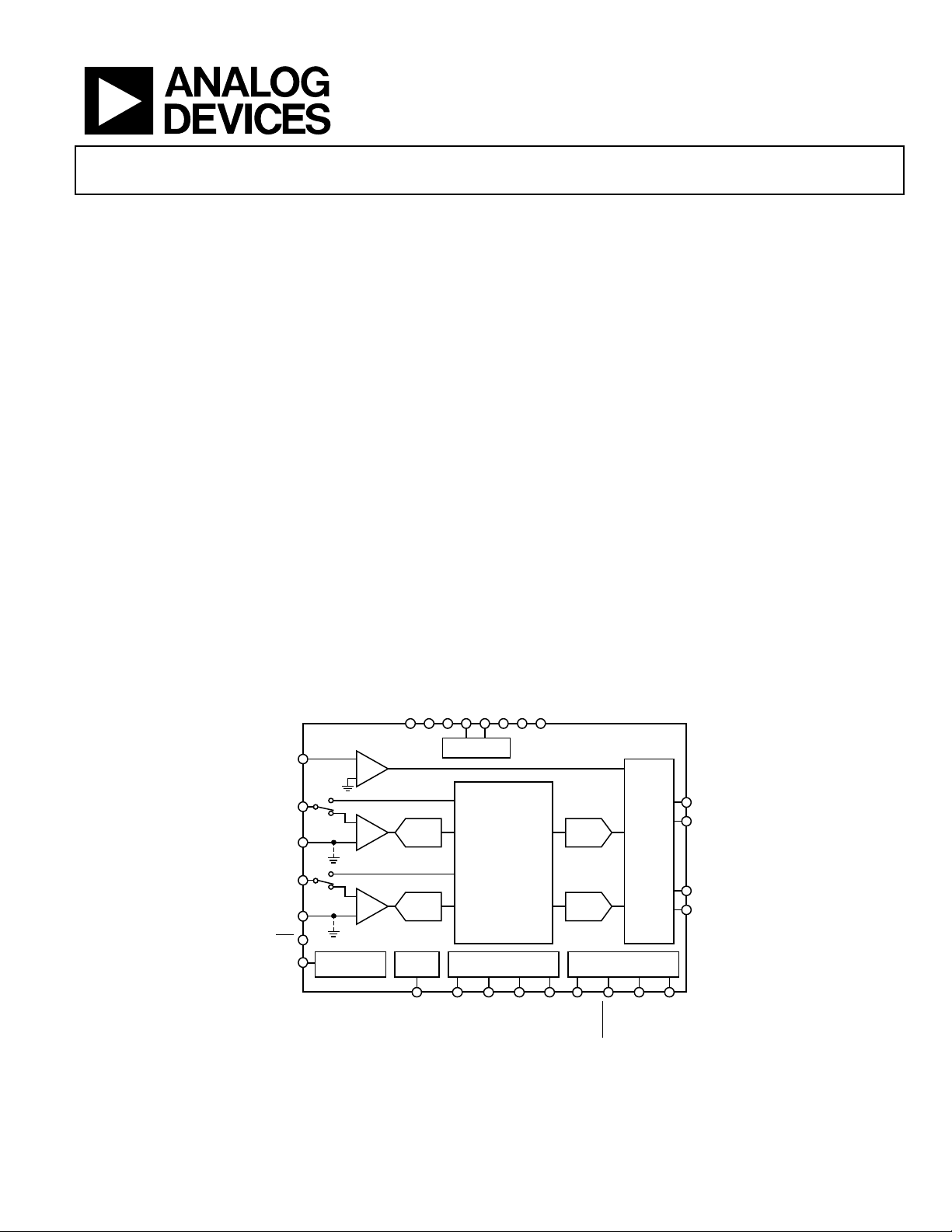
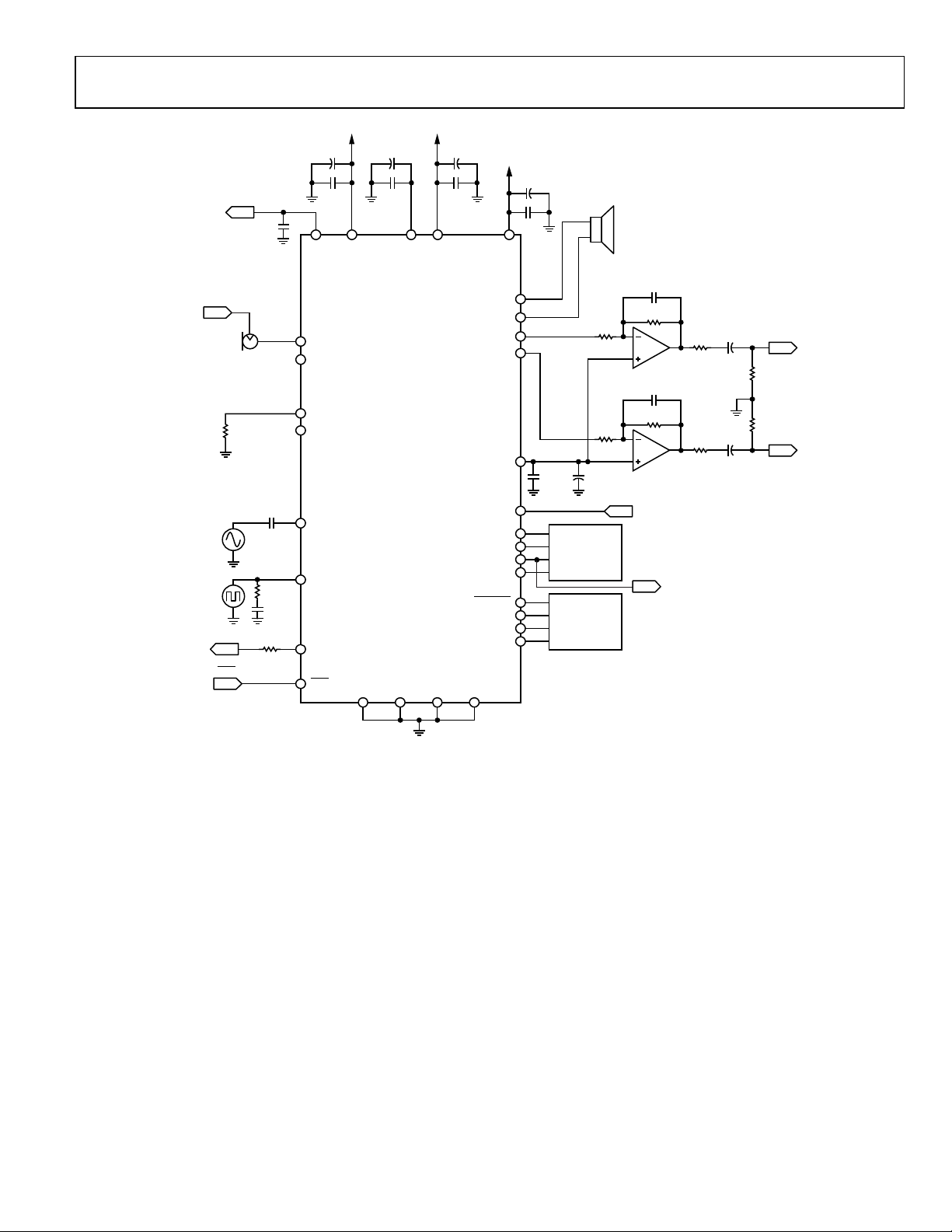
FUNCTIONAL BLOCK DIAGRAM
Recording and Playback Processing
ADAU1381
GENERAL DESCRIPTION
The ADAU1381 is a low power, 24-bit stereo audio codec. The
low noise DAC and ADC support sample rates from 8 kHz to
96 kHz. Low current draw and power saving modes make the
ADAU1381 ideal for battery-powered audio applications.
A configurable sound engine provides enhanced record and
playback processing to improve overall audio quality.
The record path includes two digital stereo microphone inputs
and an analog stereo input path. The analog inputs can be
configured for either a pseudo differential or a single-ended
stereo source. A dedicated analog beep input signal can be
mixed into any output path. The ADAU1381 includes a stereo
line output and speaker driver, which makes the device capable of
supporting dynamic speakers.
The serial control bus supports the I
the serial audio bus is programmable for I
justified, or TDM mode. A programmable PLL supports flexible
clock generation for all standard rates and available master clocks
from 11 MHz to 20 MHz.
2
C® or SPI protocols, and
2
S, left-justified, right-
CM
IOVDD
DGND
BEEP
LMIC/LMICN/
MICD1
LMICP
RMIC/RMICN/
MICD2
RMICP
PDN
MICBIAS
Rev. B
Information furnished by Analog Devices is believed to be accurate and reliable. However, no
responsibility is assumed by Analog Devices for its use, nor for any infringements of patents or other
rights of third parties that may result from its use. Specifications subject to change without notice. No
license is granted by implication or otherwise under any patent or patent rights of Analog Devices.
Trademarks and registered trademarks are the property of their respective owners.
PGA
PGA
PGA
MICROPHONE
BIAS
REGULATOR
LEFT
ADC
RIGHT
ADC
PLL
INPUT/OUTPUT PORTS
MCKI
ADC_SDATA/
DVDDOUT
AVDD1
AGND1
AVDD2
SOUND ENGINE
DECIMATION
FILTERS
WIND NOIS E
NOTCH FILTER
EQUALIZER
DIGITAL VOLUME
CONTROL
AUTOMATIC LEVEL
CONTROL
SERIAL DATA
GPIO1
BCLK/GPIO2
LRCLK/GPIO3
Figure 1.
One Technology Way, P.O. Box 9106, Norwood, MA 02062-9106, U.S.A.
Tel: 781.329.4700 www.analog.com
Fax: 781.461.3113 ©2009–2011 Analog Devices, Inc. All rights reserved.
AGND2
GPIO0
DAC_SDATA/
ADAU1381
LEFT
DAC
RIGHT
DAC
I2C/SPI
CONTROL P ORT
ADDR0/CDATA
ADDR1/CLATCH
OUTPUT
MIXER
SCL/CCLK
AOUTL
AOUTR
SPP
SPN
SDA/COUT
08313-001
Page 2

ADAU1381
TABLE OF CONTENTS
Features.............................................................................................. 1
Input Signal Path ........................................................................ 30
Applications....................................................................................... 1
General Description ......................................................................... 1
Functional Block Diagram .............................................................. 1
Revision History ............................................................................... 3
Specifications..................................................................................... 4
Record Side Performance Specifications................................... 4
Output Side Performance Specifications................................... 6
Power Supply Specifications........................................................ 8
Typical Power Management Measurements ............................. 9
Digital Filters................................................................................. 9
Digital Input/Output Specifications......................................... 10
Digital Timing Specifications ...................................................11
Absolute Maximum Ratings.......................................................... 14
Thermal Resistance .................................................................... 14
ESD Caution................................................................................ 14
Analog-to-Digital Converters................................................... 31
Digital Dual-Band Automatic Level Control (ALC) ............. 31
Playback Signal Path ...................................................................... 32
Output Signal Paths ................................................................... 32
Digital-to-Analog Converters................................................... 32
Line Outputs ............................................................................... 32
Speaker Output........................................................................... 32
Control Ports................................................................................... 33
I2C Port ........................................................................................ 33
SPI Port........................................................................................ 36
Memory and Register Access.................................................... 36
Serial Data Input/Output Ports .................................................... 38
TDM Modes................................................................................ 38
General-Purpose Input/Outputs.................................................. 40
Sound Engine.................................................................................. 41
Pin Configuration and Function Descriptions........................... 15
Typical Performance Characteristics ........................................... 17
System Block Diagrams ................................................................. 20
Theory of Operation ...................................................................... 24
Startup, Initialization, and Power................................................. 25
Power-Up Sequence ................................................................... 25
Clock Generation and Management........................................ 26
Enabling Digital Power to Functional Subsystems................ 26
Setting Up the Sound Engine.................................................... 26
Power Reduction Modes............................................................ 26
Power-Down Sequence.............................................................. 26
Clocking and Sampling Rates .......................................................27
Core Clock................................................................................... 27
Sampling Rates............................................................................ 27
PLL ............................................................................................... 28
Signal Processing........................................................................ 41
Processing Flow.......................................................................... 41
Programming.............................................................................. 41
Parameter Memory .................................................................... 41
Applications Information.............................................................. 42
Power Supply Bypass Capacitors.............................................. 42
GSM Noise Filter........................................................................ 42
Grounding................................................................................... 42
Speaker Driver Supply Trace (AVDD2) .................................. 42
Exposed Pad PCB Design ......................................................... 42
Control Register Map..................................................................... 43
Clock Management, Internal Regulator, and PLL Control... 44
Record Path Configuration....................................................... 48
Serial Port Configuration.......................................................... 53
Audio Converter Configuration............................................... 58
Record Signal Path.......................................................................... 30
Rev. B | Page 2 of 84
Playback Path Configuration.................................................... 63
Page 3

ADAU1381
Pad Configuration.......................................................................70
Outline Dimensions........................................................................84
Digital Subsystem Configuration..............................................77
REVISION HISTORY
1/11—Rev. A to Rev. B
PDN
Changes to Pin
Changes to Power-Down Pin (
Changes to Table 23 ........................................................................36
3/10—Rev. 0 to Rev. A
Changes to Output Side Performance Specifications Section
Condition Statement.....................................................................6
Added Endnote 1 to Table 3.............................................................8
Changes to Figure 23 ......................................................................20
Changes to Figure 24 ......................................................................21
Changes to Figure 25 ......................................................................22
Changes to Figure 26 ......................................................................23
Changes to Table 27 ........................................................................43
Added Register 16434 (0x4032), Dejitter Control Section ........76
Changes to Ordering Guide...........................................................84
10/09—Revision 0: Initial Version
Description in Table 10 .............................16
PDN
) Section..............................26
Ordering Guide...........................................................................84
Rev. B | Page 3 of 84
Page 4

ADAU1381
SPECIFICATIONS
Performance of all channels is identical, exclusive of the interchannel gain mismatch and interchannel phase deviation specifications.
Supply voltages AVDD = AVDD1 = AVDD2 = I/O supply = 3.3 V, digital supply = 1.5 V, unless otherwise noted; temperature = 25°C;
master clock (MCLK) = 12.288 MHz (f
word width = 24 bits; load capacitance (digital output) = 20 pF; load current (digital output) = 2 mA; high level input voltage = 0.7 × IOVDD;
and low level input voltage = 0.3 × IOVDD. All power management registers are set to their default states.
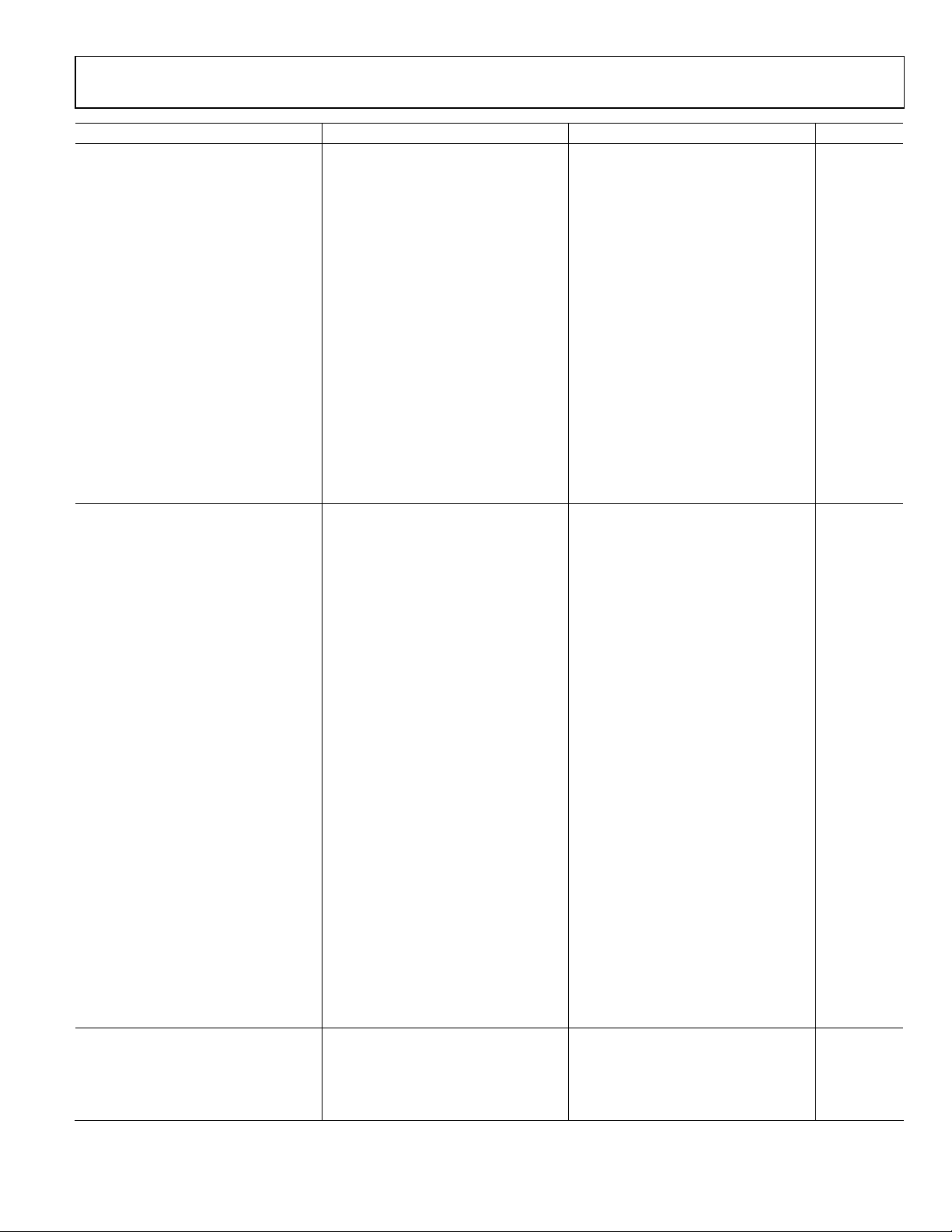
RECORD SIDE PERFORMANCE SPECIFICATIONS
Specifications guaranteed at 25°C (ambient).
Table 1.
Parameter Test Conditions/Comments Min Typ Max Unit
ANALOG-TO-DIGITAL CONVERTERS
ADC Resolution All ADCs 24 Bits
Digital Attenuation Step 0.375 dB
Digital Attenuation Range 95 dB
INPUT RESISTANCE
Noninverting Inputs PGA
(LMICP, RMICP)
Inverting Inputs PGA (LMICN, RMICN) 0 dB gain 62 kΩ
6 dB gain 32 kΩ
10 dB gain 22 kΩ
14 dB gain 14 kΩ
17 dB gain 10 kΩ
20 dB gain 8 kΩ
26 dB gain 5 kΩ
32 dB gain 4 kΩ
Beep Input PGA 0 dB 20 kΩ
6 dB 9 kΩ
10 dB 6 kΩ
14 dB 3.5 kΩ
−23 dB 50 kΩ
20 dB 2 kΩ
26 dB 2 kΩ
32 dB 2 kΩ
SINGLE-ENDED MICROPHONE INPUT
TO ADC PATH
Full-Scale Input Voltage (0 dB) Scales linearly with AVDD AVDD/3.3 V rms
AVDD = 1.8 V 0.55 (1.56) V rms (V p-p)
AVDD = 3.3 V 1.0 (2.83) V rms (V p-p)
Dynamic Range −60 dB input
With A-Weighted Filter (RMS) AVDD = 1.8 V 96 dB
AVDD = 3.3 V 94 99.2 dB
No Filter (RMS) AVDD = 1.8 V 92 dB
AVDD = 3.3 V 92 96.5 dB
Total Harmonic Distortion + Noise −3 dBFS
AVDD = 1.8 V −88 dB
AVDD = 3.3 V −90 dB
Signal-to-Noise Ratio
With A-Weighted Filter (RMS) AVDD = 1.8 V 96 dB
AVDD = 3.3 V 100 dB
No Filter (RMS) AVDD = 1.8 V 92 dB
AVDD = 3.3 V 97 dB
= 48 kHz, 256 × fS mode); input sample rate = 48 kHz; measurement bandwidth = 20 Hz to 20 kHz;
S
All gain settings 500 kΩ
Rev. B | Page 4 of 84
Page 5

ADAU1381
Parameter Test Conditions/Comments Min Typ Max Unit
Left/Right Microphone PGA Gain
Range
Left/Right Microphone PGA Mute
Attenuation
Interchannel Gain Mismatch AVDD = 3.3 V 50 mdB
Offset Error AVDD = 3.3 V 0.25 mV
Gain Error AVDD = 3.3 V −1 %
Interchannel Isolation AVDD = 3.3 V −98 dB
Power Supply Rejection Ratio CM capacitor = 10 F
AVDD = 3.3 V, 100 mV p-p at 217 Hz −55 dB
AVDD = 3.3 V, 100 mV p-p at 1 kHz −55 dB
DIFFERENTIAL MICROPHONE INPUT TO
ADC PATH
Full-Scale Input Voltage (0 dB) Scales linearly with AVDD AVDD/3.3 V rms
AVDD = 1.8 V 0.55 (1.56) V rms (V p-p)
AVDD = 3.3 V 1.0 (2.83) V rms (V p-p)
Dynamic Range −60 dB input
With A-Weighted Filter (RMS) AVDD = 1.8 V 96 dB
AVDD = 3.3 V 94 99.2 dB
No Filter (RMS) AVDD = 1.8 V 92 dB
AVDD = 3.3 V 92 96.5 dB
Total Harmonic Distortion + Noise −3 dBFS
AVDD = 1.8 V −84 dB
AVDD = 3.3 V −85 dB
Signal-to-Noise Ratio
With A-Weighted Filter (RMS) AVDD = 1.8 V 96 dB
AVDD = 3.3 V 100 dB
No Filter (RMS) AVDD = 1.8 V 92 dB
AVDD = 3.3 V 97 dB
Left/Right Microphone PGA Mute
Attenuation
Interchannel Gain Mismatch AVDD = 3.3 V 50 mdB
Offset Error AVDD = 3.3 V 0.25 mV
Gain Error AVDD = 3.3 V −1 %
Interchannel Isolation AVDD = 3.3 V −85 dB
Common-Mode Rejection Ratio AVDD = 3.3 V, 100 mV rms, 1 kHz −60 dB
AVDD = 3.3 V, 100 mV rms, 20 kHz −45 dB
BEEP TO LINE OUTPUT PATH
Full-Scale Input Voltage (0 dB) Scales linearly with AVDD AVDD/3.3 V rms
AVDD = 1.8 V 0.55 (1.56) V rms (V p-p)
AVDD = 3.3 V 1.0 (2.83) V rms (V p-p)
Total Harmonic Distortion + Noise
AVDD = 1.8 V −88 dB
AVDD = 3.3 V −88 dB
Signal-to-Noise Ratio
With A-Weighted Filter (RMS) AVDD = 1.8 V 99 dB
AVDD = 3.3 V 105 dB
No Filter (RMS) AVDD = 1.8 V 96 dB
AVDD = 3.3 V 102 dB
AVDD = 3.3 V 0 32 dB
AVDD = 3.3 V; mute set by Register
0x400E, Bit 1, and Register 0x400F, Bit 1
AVDD = 3.3 V; mute set by Register
0x400E, Bit 1, and Register 0x400F, Bit 1
−3 dBFS input, measured at AOUTL pin,
beep gain set to 0 dB
−98 dB
−98 dB
Rev. B | Page 5 of 84
Page 6

ADAU1381
Parameter Test Conditions/Comments Min Typ Max Unit
Dynamic Range −60 dB input
With A-Weighted Filter (RMS) AVDD = 1.8 V 99 dB
AVDD = 3.3 V 105 dB
No Filter (RMS) AVDD = 1.8 V 96 dB
AVDD = 3.3 V 102 dB
Beep Input Mute Attenuation
Offset Error AVDD = 3.3 V 10 mV
Gain Error AVDD = 3.3 V −0.3 dB
Interchannel Gain Mismatch 30 mdB
Beep Input PGA Gain Range AVDD = 3.3 V −23 +32 dB
Beep Playback Mixer Gain Range AVDD = 3.3 V −15 +6 dB
Power Supply Rejection Ratio CM capacitor = 10 F
AVDD = 3.3 V, 100 mV p-p at 217 Hz −58 dB
AVDD = 3.3 V, 100 mV p-p at 1 kHz −72 dB
MICROPHONE BIAS Microphone bias enabled
Bias Voltage
0.65 × AVDD AVDD = 1.8 V, low bias 1.17 V
AVDD = 3.3 V, low bias 2.145 V
0.90 × AVDD AVDD = 1.8 V, high bias 1.62 V
AVDD = 3.3 V, high bias 2.97 V
Bias Current Source
Noise in the Signal Bandwidth AVDD = 3.3 V, 20 Hz to 20 kHz
High bias, high performance 39 nV√Hz
High bias, low performance 78 nV√Hz
Low bias, high performance 25 nV√Hz
Low bias, low performance 35 nV√Hz
AVDD = 1.8 V, 20 Hz to 20 kHz
High bias, high performance 35 nV√Hz
High bias, low performance 45 nV√Hz
Low bias, high performance 23 nV√Hz
Low bias, low performance 23 nV√Hz
AVDD = 3.3 V; mute set by
Register 0x4008, Bit 3
AVDD = 3.3 V, high bias, high
performance
−90 dB
5 mA
OUTPUT SIDE PERFORMANCE SPECIFICATIONS
Specifications guaranteed at 25°C (ambient). The output load for the speaker output path is an 8 Ω, 400 mW speaker.
Table 2.
Parameter Test Conditions/Comments Min Typ Max Unit
DIGITAL-TO-ANALOG CONVERTERS
DAC Resolution All DACs 24 Bits
Digital Attenuation Step 0.375 dB
Digital Attenuation Range 95 dB
DAC TO LINE OUTPUT PATH
Full-Scale Output Voltage (0 dB) Scales linearly with AVDD AVDD/3.3 V rms
AVDD = 1.8 V 0.55 (1.56) V rms (V p-p)
AVDD = 3.3 V 1.0 (2.83) V rms (V p-p)
Line Output Mute Attenuation,
DAC to Mixer Path Muted
Line Output Mute Attenuation,
Line Output Muted
AVDD = 3.3 V; mute set by Register
0x401C, Bit 5, and Register 0x401E, Bit 6
AVDD = 3.3 V; mute set by Register
0x4025, Bit 1, and Register 0x4026, Bit 1
Rev. B | Page 6 of 84
−85 dB
−85 dB
Page 7
ADAU1381
Parameter Test Conditions/Comments Min Typ Max Unit
Dynamic Range −60 dB input
With A-Weighted Filter (RMS) AVDD = 1.8 V 99 dB
AVDD = 3.3 V 94 103 dB
No Filter (RMS) AVDD = 1.8 V 97 dB
AVDD = 3.3 V 92 100 dB
Total Harmonic Distortion + Noise −3 dBFS dB
AVDD = 1.8 V −88 dB
AVDD = 3.3 V −88 dB
Signal-to-Noise Ratio
With A-Weighted Filter (RMS) AVDD = 1.8 V 99 dB
AVDD = 3.3 V 103 dB
No Filter (RMS) AVDD = 1.8 V 97 dB
AVDD = 3.3 V 100 dB
Power Supply Rejection Ratio CM capacitor = 10 F
AVDD = 3.3 V, 100 mV p-p at 217 Hz −55 dB
AVDD = 3.3 V, 100 mV p-p at 1 kHz −63 dB
Gain Error AVDD = 3.3 V −1 dB
Interchannel Gain Mismatch AVDD = 3.3 V 50 mdB
Offset Error AVDD = 3.3 V 10 mV
DAC TO SPEAKER OUTPUT PATH PO = output power
Differential Full-Scale Output Voltage
(0 dB)
AVDD = 1.8 V 1.1 (3.12) V rms (V p-p)
AVDD = 3.3 V 2.0 (5.66) V rms (V p-p)
Total Harmonic Distortion + Noise
4 Ω Load AVDD = 1.8 V, PO = 50 mW −60 dB
AVDD = 3.3 V, PO = 175 mW −60 dB
8 Ω Load AVDD = 1.8 V, PO = 50 mW −60 dB
AVDD = 3.3 V, PO = 175 mW −60 dB
AVDD = 3.3 V, PO = 330 mW −60 dB
AVDD = 3.3 V, PO = 440 mW −16 dB
Dynamic Range −60 dB input
With A-Weighted Filter (RMS) AVDD = 1.8 V 100 dB
AVDD = 3.3 V 94 105 dB
No Filter (RMS) AVDD = 1.8 V 98 dB
AVDD = 3.3 V 92 103 dB
Signal-to-Noise Ratio
With A-Weighted Filter (RMS) AVDD = 1.8 V 100 dB
AVDD = 3.3 V 105 dB
No Filter (RMS) AVDD = 1.8 V 98 dB
AVDD = 3.3 V 103 dB
Power Supply Rejection Ratio CM capacitor = 10 F
AVDD = 3.3 V,100 mV p-p at 217 Hz −55 dB
AVDD = 3.3 V, 100 mV p-p at 1 kHz −55 dB
Differential Offset Error AVDD = 3.3 V 2 mV
Mono Mixer Mute Attenuation,
DAC to Mixer Path Muted
BEEP TO SPEAKER OUTPUT PATH PO = output power
Differential Full-Scale Output Voltage
(0 dB)
AVDD = 1.8 V 1.1 (3.12) V rms (V p-p)
AVDD = 3.3 V 2.0 (5.66) V rms (V p-p)
Scales linearly with AVDD AVDD/1.65 V rms
Mute set by Register 0x401F, Bit 0 −90 dB
Scales linearly with AVDD AVDD/1.65 V rms
Rev. B | Page 7 of 84
Page 8
ADAU1381
Parameter Test Conditions/Comments Min Typ Max Unit
Total Harmonic Distortion + Noise
8 Ω, 1 nF load, AVDD = 1.8 V, PO = 50 mW −60 dB
AVDD = 3.3 V, PO = 175 mW −60 dB
Dynamic Range −60 dB input
With A-Weighted Filter (RMS) AVDD = 1.8 V 97 dB
AVDD = 3.3 V 103 dB
No Filter (RMS) AVDD = 1.8 V 94 dB
AVDD = 3.3 V 100 dB
Signal-to-Noise Ratio
With A-Weighted Filter (RMS) AVDD = 1.8 V 98 dB
AVDD = 3.3 V 103 dB
No Filter (RMS) AVDD = 1.8 V 96 dB
AVDD = 3.3 V 101 dB
Power Supply Rejection Ratio CM capacitor = 10 F
100 mV p-p at 217 Hz −57 dB
100 mV p-p at 1 kHz −60 dB
Differential Offset Error 2 mV
Mono Mixer Mute Attenuation,
Beep to Mixer Path Muted
REFERENCE (CM PIN)
Common-Mode Reference Output AVDD/2 V
Mute set by Register 0x401F, Bit 0 −90 dB
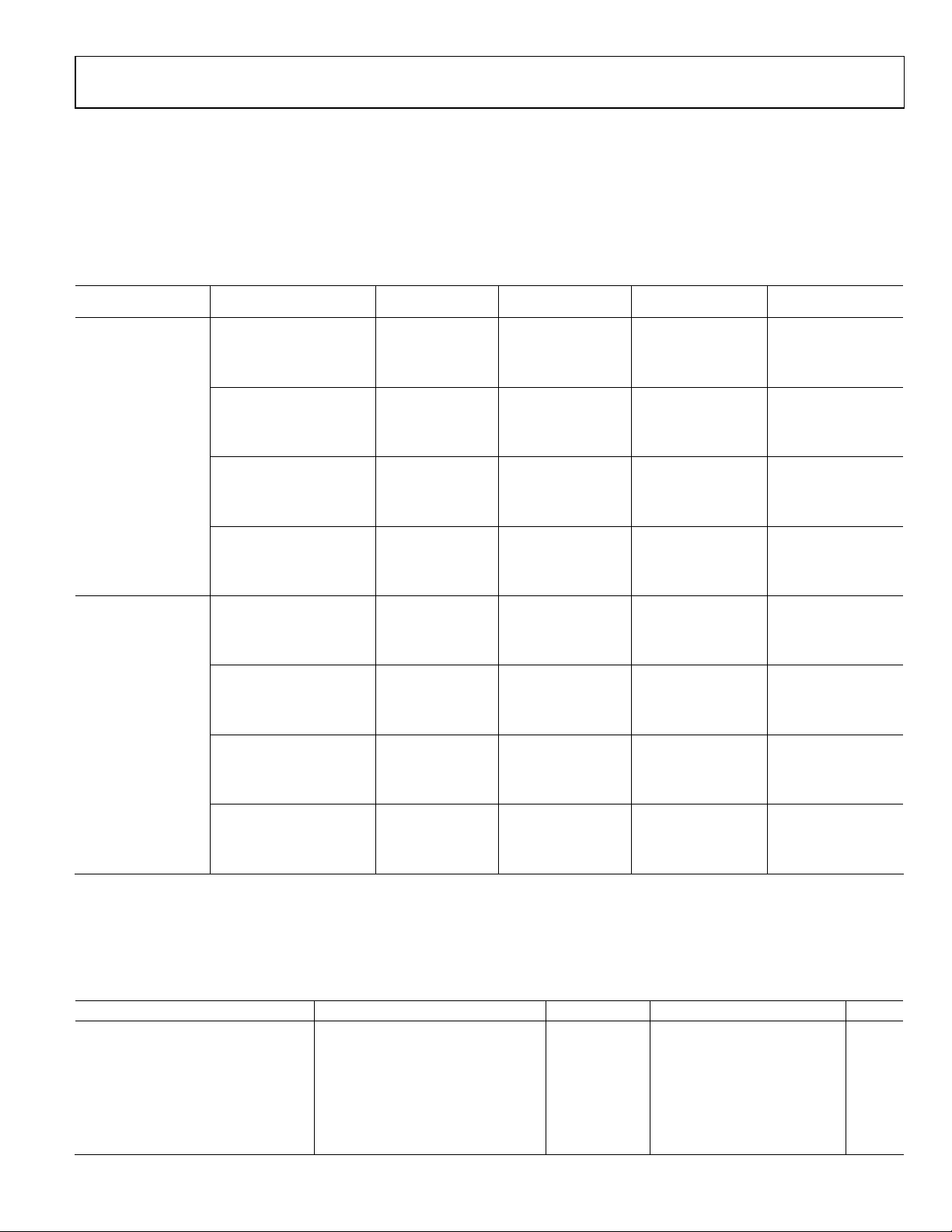
POWER SUPPLY SPECIFICATIONS
AVDD1 and AVDD2 must always be equal. Power supply measurements are taken with the sound engine processing path enabled.
Table 3.
Parameter Test Conditions/Comments Min Typ Max Unit
AVDD1, AVDD2 1.81 3.3 3.65 V
IOVDD 1.63 3.3 3.65 V
Digital I/O Current (IOVDD = 3.3 V) 20 pF capacitive load on all digital pins
= 48 kHz 0.20 mA
Slave Mode, Analog I/O,
12.288 MHz External MCLK Input
f
f
Master Mode, MCKO Disabled fS = 48 kHz 1.25 mA
f
f
Digital I/O Current (IOVDD = 1.8 V) 20 pF capacitive load on all digital pins
Slave Mode, Analog I/O,
12.288 MHz External MCLK Input
f
f
Master Mode, MCKO Disabled fS = 48 kHz 0.68 mA
f
f
Analog Current (AVDD) See Table 4
1
The zero-cross detection of the beep path is not supported at AVDD1, AVDD2 < 2.2 V.
f
S
= 96 kHz 0.35 mA
S
= 8 kHz 0.04 mA
S
= 96 kHz 2.50 mA
S
= 8 kHz 0.22 mA
S
= 48 kHz 0.10 mA
f
S
= 96 kHz 0.18 mA
S
= 8 kHz 0.02 mA
S
= 96 kHz 1.33 mA
S
= 8 kHz 0.12 mA
S
Rev. B | Page 8 of 84
Page 9
ADAU1381
TYPICAL POWER MANAGEMENT MEASUREMENTS
Master clock = 12.288 MHz, PLL is active in integer mode at a 256 × fS input rate for fS = 48 kHz, analog and digital input tones are
−1 dBFS with a frequency of 1 kHz. Analog input and output are simultaneously active. Pseudo differential stereo input is routed to
ADCs, and DACs are routed to stereo line output with a 16 k load. ADC input at −1 dBFS, DAC input at 0 dBFS. The speaker output is
disabled. The serial port is configured in slave mode. The beep path is disabled. The sound engine processing path is enabled. Current
measurements are given in units of mA rms.
Table 4. Mixer Boost and Power Management Conditions
Typical AVDD Current
Operating Voltage Power Management Mode1 Mixer Boost Mode2
AVDD = IOVDD = 3.3 V Normal (default) Normal operation 16.84 88.5 93.0
Boost Level 1 16.88 88.5 93.0
Boost Level 2 16.92 88.5 93.0
Boost Level 3 17.00 88.5 93.0
Extreme power saving Normal operation 15.66 88.0 87.5
Boost Level 1 15.68 88.0 87.5
Boost Level 2 15.70 88.0 87.5
Boost Level 3 15.75 88.0 87.5
Enhanced performance Normal operation 17.43 88.5 94.5
Boost Level 1 17.50 88.5 94.5
Boost Level 2 17.53 88.5 94.5
Boost Level 3 17.63 88.5 94.5
Power saving Normal operation 16.25 89.0 90.5
Boost Level 1 16.28 89.0 90.5
Boost Level 2 16.31 89.0 90.5
Boost Level 3 16.38 89.0 90.5
AVDD = IOVDD = 1.8 V Normal (default) Normal operation 15.15 88.5 89.5
Boost Level 1 15.19 88.5 89.5
Boost Level 2 15.23 88.5 89.5
Boost Level 3 15.30 88.5 89.5
Extreme power saving Normal operation 14.03 86.5 85.5
Boost Level 1 14.05 86.5 85.5
Boost Level 2 14.07 86.5 85.5
Boost Level 3 14.12 86.5 85.5
Enhanced performance Normal operation 15.71 88.5 90.5
Boost Level 1 15.76 88.5 90.5
Boost Level 2 15.81 88.5 90.5
Boost Level 3 15.89 88.5 90.5
Power saving Normal operation 14.59 88.0 88.0
Boost Level 1 14.62 88.0 88.0
Boost Level 2 14.65 88.0 88.0
Boost Level 3 14.71 88.0 88.0
1
Set by Register 0x4009, Bits[4:1], and Register 0x4029, Bits[5:2].
2
Set by Register 0x4009, Bits[6:5].
Consumption (mA)
Typical ADC
THD + N (dB)
Typical Line Output
THD + N (dB)
DIGITAL FILTERS
Table 5.
Parameter Mode Factor Min Typ Max Unit
ADC DECIMATION FILTER
Pass Band 0.4375 × f
Pass-Band Ripple ±0.015 dB
Transition Band 0.5 × f
Stop Band 0.5625 × f
Stop-Band Attenuation 70 dB
Group Delay 22.9844/f
All modes, typ value is for 48 kHz
Rev. B | Page 9 of 84
S
S
S
S
21 kHz
24 kHz
27 kHz
479 µs
Page 10
ADAU1381
Parameter Mode Factor Min Typ Max Unit
DAC INTERPOLATION FILTER
Pass Band 48 kHz mode, typ value is for 48 kHz 0.4535 × f
96 kHz mode, typ value is for 96 kHz 0.3646 × f
Pass-Band Ripple 48 kHz mode, typ value is for 48 kHz ±0.01 dB
96 kHz mode, typ value is for 96 kHz ±0.05 dB
Transition Band 48 kHz mode, typ value is for 48 kHz 0.5 × f
96 kHz mode, typ value is for 96 kHz 0.5 × f
S
S
Stop Band 48 kHz mode, typ value is for 48 kHz 0.5465 × f
96 kHz mode, typ value is for 96 kHz 0.6354 × f
Stop-Band Attenuation 48 kHz mode, typ value is for 48 kHz 70 dB
96 kHz mode, typ value is for 96 kHz 70 dB
Group Delay 48 kHz mode, typ value is for 48 kHz 25/f
96 kHz mode, typ value is for 96 kHz 11/f
S
S
DIGITAL INPUT/OUTPUT SPECIFICATIONS
−25°C < TA < +85°C, IOVDD = 1.62 V to 3.63 V, unless otherwise specified.
Table 6.
Parameter Conditions/Comments Min Typ Max Unit
HIGH LEVEL INPUT VOLTAGE (VIH) 0.7 × IOVDD V
LOW LEVEL INPUT VOLTAGE (VIL) IOVDD ≥ 2.97 V 0.3 × IOVDD V
1.8 V ≤ IOVDD ≤ 2.97 V 0.2 × IOVDD V
IOVDD < 1.8 V 0.1 × IOVDD V
INPUT LEAKAGE IIH at VIH = 2.4 V ±0.17 µA
I
I
I
I
I
I
HIGH LEVEL OUTPUT VOLTAGE (VOH)
LOW LEVEL OUTPUT VOLTAGE (VOL)
INPUT CAPACITANCE 5 pF
at VIL = 0.8 V ±0.17 µA
IL
of MCKI −7 µA
IL
with internal pull-up ±0.7 µA
IH
with internal pull-down −7 µA
IL
with internal pull-up 5 µA
IH
with internal pull-down ±0.18 µA
IL
For low drive strength, I
at IOVDD = 3.3 V, I
IOVDD = 1.8 V; for high drive strength, I
and I
= 3 mA at IOVDD = 3.3 V, IOH = 0.9 mA and
OL
= 0.9 mA at IOVDD = 1.8 V
I
OL
For low drive strength, I
at IOVDD = 3.3 V, I
IOVDD = 1.8 V; for high drive strength, I
and I
= 3 mA at IOVDD = 3.3 V, IOH = 0.9 mA and
OL
= 0.9 mA at IOVDD = 1.8 V
I
OL
= 2 mA and IOL = 2 mA
OH
= 0.6 mA and IOL = 0.6 mA at
OH
= 2 mA and IOL = 2 mA
OH
= 0.6 mA and IOL = 0.6 mA at
OH
= 3 mA
OH
= 3 mA
OH
22 kHz
S
35 69 kHz
S
24 kHz
48 kHz
26 kHz
S
61 kHz
S
521 µs
115 µs
IOVDD − 0.4 V
0.4 V
Rev. B | Page 10 of 84
Page 11
ADAU1381
DIGITAL TIMING SPECIFICATIONS
−25°C < TA < +85°C, IOVDD = 1.62 V to 3.63 V, unless otherwise specified.
Table 7. Digital Timing
Limit
Parameter t
MASTER CLOCK
tMP 50 90.9 ns Master clock (MCLK) period (that is, period of the signal input to MCKI).
Duty Cycle 30 70 %
SERIAL PORT
t
10 ns BCLK pulse width low.
BIL
t
10 ns BCLK pulse width high.
BIH
t
5 ns LRCLK setup. Time to BCLK rising.
LIS
t
5 ns LRCLK hold. Time from BCLK rising.
LIH
t
5 ns DAC_SDATA setup. Time to BCLK rising.
SIS
t
5 ns DAC_SDATA hold. Time from BCLK rising.
SIH
t
70 ns ADC_SDATA delay. Time from BCLK falling in master mode.
SODM
SPI PORT
f
5 MHz CCLK frequency, read operation, IOVDD = 1.8 V ± 10%.
CCLK,R
f
10 MHz CCLK frequency, read operation, IOVDD = 3.3 V ± 10%.
CCLK,R
f
25 MHz CCLK frequency, write operation, IOVDD = 1.8 V ± 10%.
CCLK,W
f
25 MHz CCLK frequency, write operation, IOVDD = 3.3 V ± 10%.
CCLK,W
t
10 ns CCLK pulse width low.
CCPL
t
10 ns CCLK pulse width high.
CCPH
t
10 ns
CLS
t
5 ns
CLH
t
10 ns
CLPH
t
5 ns CDATA setup. Time to CCLK rising.
CDS
t
5 ns CDATA hold. Time from CCLK rising.
CDH
t
70 COUT delay from CCLK edge to valid data, IOVDD = 1.8 V ± 10%.
COD
40 ns COUT delay from CCLK edge to valid data, IOVDD = 3.3 V ± 10%.
I2C PORT
f
400 kHz SCL frequency.
SCL
t
0.6 µs SCL high.
SCLH
t
1.3 µs SCL low.
SCLL
t
0.6 µs Setup time; relevant for repeated start condition.
SCS
t
0.6 µs Hold time. After this period, the first clock is generated.
SCH
tDS 100 ns Data setup time.
t
300 ns SCL rise time.
SCR
t
300 ns SCL fall time.
SCF
t
300 ns SDA rise time.
SDR
t
300 ns SDA fall time.
SDF
t
0.6 µs Bus-free time. Time between stop and start.
BFT
DIGITAL MICROPHONE RL = 1 MΩ, CL = 14 pF.
t
10 ns Digital microphone clock fall time.
DCF
t
10 ns Digital microphone clock rise time.
DCR
t
22 30 ns Digital microphone delay time for valid data.
DDV
t
0 12 ns Digital microphone delay time for data three-stated.
DDH
t
MIN
MAX
Unit Description
setup. Time to CCLK rising.
CLATCH
hold. Time from CCLK rising.
CLATCH
pulse width high.
CLATCH
Rev. B | Page 11 of 84
Page 12
ADAU1381
Digital Timing Diagrams
t
LIH
t
SIS
LSB
t
SIH
08313-002
BCLK
LRCLK
DAC_SDATA
LEFT-JUSTIFIED
RIGHT-JUSTIFIED
MODE
DAC_SDATA
2
I
S MODE
DAC_SDATA
MODE
t
BIH
t
BIL
t
LIS
t
SIS
MSB
t
SIH
8-BIT CLOCKS
(24-BIT DATA)
12-BIT CLO CKS
(20-BIT DATA)
14-BIT CLO CKS
(18-BIT DATA)
16-BIT CLO CKS
(16-BIT DATA)
MSB – 1
t
SIS
MSB
t
SIH
t
SIS
MSB
t
SIH
Figure 2. Serial Input Port Timing
BCLK
LRCLK
ADC_SDATA
LEFT-JUSTIFIED
MODE
ADC_SDATA
2
I
S MODE
ADC_SDATA
RIGHT-JUSTIFIED
MODE
t
BIH
t
BIL
t
SODM
MSB
8-BIT CLO CKS
(24-BIT DAT A)
12-BIT CLOCKS
(20-BIT DAT A)
14-BIT CLOCKS
(18-BIT DAT A)
16-BIT CLOCKS
(16-BIT DAT A)
t
SODM
MSB – 1
MSB
t
SODM
MSB
LSB
08313-003
Figure 3. Serial Output Port Timing
Rev. B | Page 12 of 84
Page 13
ADAU1381
t
CLS
t
CCPL
CLATCH
CCLK
CDATA
COUT
t
CCPH
t
t
CDS
CDH
Figure 4. SPI Port Timing
t
t
SDR
SCR
t
DS
t
SDF
t
SCLL
t
SCLH
t
SCF
Figure 5. I
2
C Port Timing
t
SCS
t
SCH
SDA
SCL
t
SCH
t
CLH
t
COD
t
BFT
08313-005
t
CLPH
08313-004
t
CLK
DATA1/
DATA1 DATA1 DATA2DATA2
DATA2
DCF
t
DDH
t
DDV
t
DDH
Figure 6. Digital Microphone Timing
t
DCR
t
DDV
08313-106
Rev. B | Page 13 of 84
Page 14
ADAU1381
ABSOLUTE MAXIMUM RATINGS
Table 8.
Parameter Rating
Power Supply (AVDD1 = AVDD2) −0.3 V to +3.9 V
Input Current (Except Supply Pins) ±20 mA
Analog Input Voltage (Signal Pins) –0.3 V to VDD + 0.3 V
Digital Input Voltage (Signal Pins) −0.3 V to VDD + 0.3 V
Operating Temperature Range (Case) −25°C to +85°C
Storage Temperature Range −65°C to +150°C
Stresses above those listed under Absolute Maximum Ratings
may cause permanent damage to the device. This is a stress
rating only; functional operation of the device at these or any
other conditions above those indicated in the operational
section of this specification is not implied. Exposure to absolute
maximum rating conditions for extended periods may affect
device reliability.
THERMAL RESISTANCE
In Ta b le 9 , θJA is the junction-to-ambient thermal resistance, θJB is
the junction-to-board thermal resistance, θ
thermal resistance, ψ
mal resistance, and ψ
is the in-use junction-to-top of package ther-
JB
is the in-use junction-to-board thermal
JT
is the junction-to-case
JC
resistance. All characteristics are for a 4-layer board.
Table 9. Thermal Resistance
Package Type θ
32-Lead LFCSP 35 19 2.5 18 0.3 °C/W
30-Ball WLCSP 39 7 0.5 °C/W
JA
θJB θ
JC
ψJB ψJT Unit
ESD CAUTION
Rev. B | Page 14 of 84
Page 15
ADAU1381
PIN CONFIGURATION AND FUNCTION DESCRIPTIONS
MICBIAS
BEEP
LMIC/LMICN/MICD1
LMICP
RMICP
RMIC/RMICN/MICD2
AOUTL
AOUTR
27
26
25
29
28
31
30
32
1CM
PIN 1
2PDN
INDICATOR
3AGND1
4AVDD1
ADAU1381
5DVDDOUT
6DGND
7GPIO
8SCL/CCLK
NOTES
1. NC = NO CONNECT.
2. THE EXPOSED PAD IS CONNECTED INTERNALLY TO THE
ADAU1381 GROUNDS. F OR INCREASED RELIABILIT Y OF THE
SOLDER JOINTS AND MAXIMUM THERMAL CAPABILITY, IT IS
RECOMMENDED THAT THE PAD BE SOL DE RE D TO THE
GROUND PLANE.
TOP VIEW
(Not to Scale)
9
11
12
10
IOVDD
SDA/COUT
ADDR0/CDATA
ADDR1/CLATCH
13
DAC_SDATA/GPIO0
24 NC
23 AGND2
22 SPP
21 NC
20 SPN
19 AVDD2
18 MCKO
17 MCKI
14
15
16
BCLK/GPIO2
LRCLK/GPIO3
ADC_SDATA/GPIO1
08313-007
Figure 7. 32-Lead LFCSP Pin Configuration
1
AGND2 AOUTL RMICP
A
SPP AOUTR
B
234
RMIC/
RMICN/
MICD2
LMIC/
LIMICN/
MICD1
LMICP BEEP AGND1
MICBIAS CM
56
C
AVDD2 MCKO
D
MCKI
E
SPN
LRCLK/
GPIO3
BCLK/
GPIO2
ADDR0/
CDATA
ADC_
SDATA/
GPIO1
DAC_
SDATA/
GPIO0
(BALL SIDE DOWN)
ADDR1/
CLATCH
TOP VIEW
Not to Scale
SCL/
CCLK
IOVDD
PDN AVDD1
GPIO DVDDOUT
SDA/
COUT
DGND
8313-008
Figure 8. 30-Ball, 6 × 5 WLCSP Pin Configuration (Bottom View)
Rev. B | Page 15 of 84
Page 16
ADAU1381
Table 10. Pin Function Descriptions
Pin No.
LFCSP WLCSP Mnemonic Type1 Description
1 A6 CM A_OUT
2 C5
PDN
A_IN
3 B6 AGND1 PWR Analog Ground.
4 C6 AVDD1 PWR Analog Power Supply. Should be equivalent to AVDD2.
5 D6 DVDDOUT PWR
6 E6 DGND PWR Digital Ground.
7 D5 GPIO D_IO Dedicated General-Purpose Input/Output.
8 C4 SCL/CCLK D_IN I2C Clock/SPI Clock.
9 E5 SDA/COUT D_IO I2C Data/SPI Data Output.
10 C3 ADDR0/CDATA D_IN I2C Address 0/SPI Data Input.
11 D4
ADDR1/CLATCH
D_IN I
12 E4 IOVDD PWR
13 E3 DAC_SDATA/GPIO0 D_IO DAC Serial Input Data/General-Purpose Input and Output.
14 D3 ADC_SDATA/GPIO1 D_IO ADC Serial Output Data/General-Purpose Input and Output.
15 E2 BCLK/GPIO2 D_IO Serial Data Port Bit Clock/General-Purpose Input and Output.
16 C2 LRCLK/GPIO3 D_IO Serial Data Port Frame Clock/General-Purpose Input and Output.
17 E1 MCKI D_IN Master Clock Input.
18 D2 MCKO D_OUT Master Clock Output.
19 D1 AVDD2 PWR Analog Power Supply. Should be equivalent to AVDD1.
20 C1 SPN A_OUT Speaker Amplifier Negative Signal Output.
21 N/A NC No Connect.
22 B1 SPP A_OUT Speaker Amplifier Positive Signal Output.
23 A1 AGND2 PWR Speaker Amplifier Ground.
24 N/A NC No Connect.
25 B2 AOUTR A_OUT Line Output Amplifier, Right Channel.
26 A2 AOUTL A_OUT Line Output Amplifier, Left Channel.
27 B3 RMIC/RMICN/MICD2 A_IN
28 A3 RMICP A_IN Right Channel Input from Positive Pseudo Differential Source.
29 B4 LMICP A_IN Left Channel Input from Positive Pseudo Differential Source.
30 A4 LMIC/LMICN/MICD1 A_IN
31 B5 BEEP A_IN Beep Signal Input.
32 A5 MICBIAS PWR Microphone Bias.
THERM_PAD
(Exposed Pad)
1
A_OUT = analog output, A_IN = analog input, PWR = power, D_IO = digital input/output, D_OUT = digital output, and D_IN = digital input.
VDD/2 V Common-Mode Reference. A 10 F to 47 F decoupling capacitor should be
connected between this pin and ground to reduce crosstalk between the ADCs and
DACs. The material of the capacitors is not critical. This pin can be used to bias external
analog circuits, as long as they are not drawing current from CM (for example, the
noninverting input of an op amp).
Power-Down. Connecting this pin to GND powers down the chip. Resides in AVDD1
domain.
Digital Core Supply Decoupling Point. The digital supply is generated from an onboard regulator and does not require an external supply. DVDDOUT should be
decoupled to DGND with a 100 nF capacitor.
2
C Address 1/SPI Latch Signal.
Supply for Digital Input and Output Pins. The digital output pins are supplied from
IOVDD, which sets the highest allowed input voltage for the digital input pins. The
current draw of this pin is variable because it is dependent on the loads of the digital
outputs. IOVDD should be decoupled to DGND with a 100 nF capacitor.
Right Channel Input from Single-Ended Source/Right Channel Input from Negative
Pseudo Differential Source/Digital Microphone Input 2.
Left Channel Input from Single-Ended Source/Left Channel Input from Negative
Pseudo Differential Source/Digital Microphone Input 1.
Exposed Pad. The exposed pad is connected internally to the ADAU1381 grounds. For
increased reliability of the solder joints and maximum thermal capability, it is
recommended that the pad be soldered to the ground plane.
Rev. B | Page 16 of 84
Page 17
ADAU1381
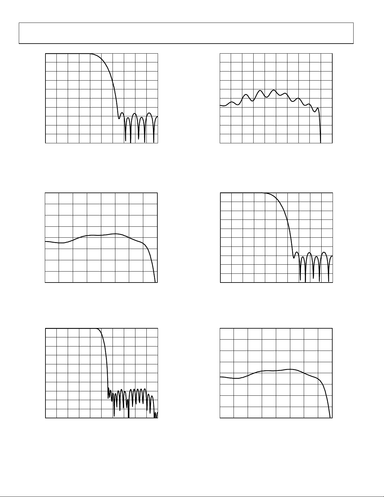
TYPICAL PERFORMANCE CHARACTERISTICS
0
–10
–20
–30
–40
–50
–60
MAGNITUDE (dBFS)
–70
–80
–90
–100
0 0.1 0.2 0.3 0.4 0.5 0.6 0.7 0.8 0.9 1.0
FREQUENCY (NO RM ALIZED TO
f
)
S
Figure 9. ADC Decimation Filter, 64× Oversampling,
Normalized to f
S
08313-009
0.10
0.08
0.06
0.04
0.02
0
–0.02
MAGNITUDE (dBFS)
–0.04
–0.06
–0.08
–0.10
0 0.05 0.10 0.15 0.20 0.25 0.30 0.35 0.40 0.45 0.50
FREQUENCY (NORMALIZED TO
f
)
S
Figure 12. ADC Decimation Filter Pass-Band Ripple, 128× Oversampling,
Normalized to f
S
08313-012
0.04
0.02
0
–0.02
MAGNITUDE (dBFS)
–0.04
–0.06
0.400.350.300.250.200.150.100.050
FREQUENCY (NORMALIZED TO
f
)
S
Figure 10. ADC Decimation Filter Pass-Band Ripple, 64× Oversampling,
Normalized to f
0
–10
–20
–30
–40
–50
–60
MAGNITUDE (d BF S)
–70
–80
–90
–100
0 0.1 0.2 0.3 0.4 0.5 0.6 0.7 0.8 0.9 1.0
FREQUENCY (NO RM ALIZED TO
S
f
)
S
Figure 11. ADC Decimation Filter, 128× Oversampling,
Normalized to f
S
0
–10
–20
–30
–40
–50
–60
MAGNITUDE (d BFS)
–70
–80
–90
–100
0 0.1 0.2 0.3 0.4 0.5 0.6 0.7 0.8 0.9 1.0
08313-010
FREQUENCY (NO RM ALIZED TO
f
)
S
08313-013
Figure 13. ADC Decimation Filter, Double-Rate Mode,
Normalized to f
0.04
0.02
0
–0.02
MAGNITUDE (dBFS)
–0.04
–0.06
08313-011
14. ADC Decimation Filter Pass-Band Ripple, Double-Rate Mode,
Figure
FREQUENCY (NORMALIZED TO
Normalized to f
S
0.400.350.300.250.200.150.100.050
f
)
S
S
08313-014
Rev. B | Page 17 of 84
Page 18
ADAU1381
0
–10
–20
–30
–40
–50
–60
MAGNITUDE (dBFS)
–70
–80
–90
–100
0 0.1 0.2 0.3 0.4 0.5 0.6 0.7 0.8 0.9 1.0
FREQUENCY (NO RM ALIZED TO
f
)
S
Figure 15. DAC Interpolation Filter, 64× Oversampling,
Normalized to f
S
08313-015
0.05
0.04
0.03
0.02
0.01
0
–0.01
MAGNITUDE (dBFS)
–0.02
–0.03
–0.04
–0.05
0 0.05 0.10 0.15 0.20 0.25 0.30 0.35 0.40 0.45 0.50
FREQUENCY (NORMALIZED TO
f
)
S
Figure 18. DAC Interpolation Filter Pass-Band Ripple, 128× Oversampling,
Normalized to f
S
08313-018
0.20
0.15
0.10
0.05
0
–0.05
MAGNITUDE (dBFS)
–0.10
–0.15
–0.20
0 0.05 0.10 0.15 0.20 0.25 0.30 0.35 0.40
FREQUENCY (NORMALIZED TO
f
)
S
Figure 16. DAC Interpolation Filter Pass-Band Ripple, 64× Oversampling,
Normalized to f
0
–10
–20
–30
–40
–50
–60
MAGNITUDE (dBFS)
–70
–80
–90
–100
0 0.1 0.2 0.3 0.4 0.5 0.6 0.7 0.8 0.9 1.0
FREQUENCY (NO RM ALIZED TO
S
f
)
S
08313-017
Figure 17. DAC Interpolation Filter, 128× Oversampling,
Normalized to f
S
0
–10
–20
–30
–40
–50
–60
MAGNITUDE (dBFS)
–70
–80
–90
–100
0 0.1 0.2 0.3 0.4 0.5 0.6 0.7 0.8 0.9 1.0
08313-016
FREQUENCY (NO RM ALIZED TO
f
)
S
08313-019
Figure 19. DAC Interpolation Filter, Double-Rate Mode,
Normalized to f
0.20
0.15
0.10
0.05
0
–0.05
MAGNITUDE (dBFS)
–0.10
–0.15
–0.20
0 0.05 0.10 0.15 0.20 0.25 0.30 0.35 0.40
FREQUENCY (NORMALIZED TO
S
f
)
S
08313-020
Figure 20. DAC Interpolation Filter Pass-Band Ripple, Double-Rate Mode,
Normalized to f
S
Rev. B | Page 18 of 84
Page 19
ADAU1381
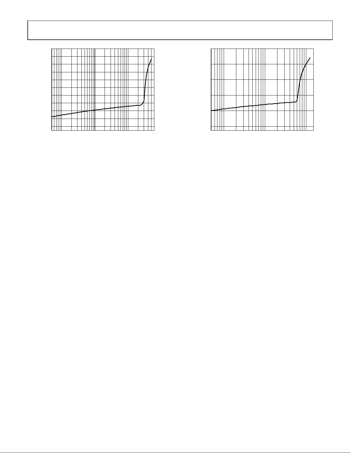
0
–10
–20
–30
–40
–50
–60
THD + N (dB)
–70
–80
–90
–100
SPEAKER OUTPUT P O WER (mW)
600100101
08313-121
Figure 21. THD + N vs. Speaker Output Power, 8 Ω Load, 3.3 V Supply Figure 22. THD + N vs. Speaker Output Power, 8 Ω Load, 1.8 V Supply
THD + N (dB)
–20
–40
–60
–80
–100
0
SPEAKER OUTPUT P O WER (mW)
100101
08313-122
Rev. B | Page 19 of 84
Page 20
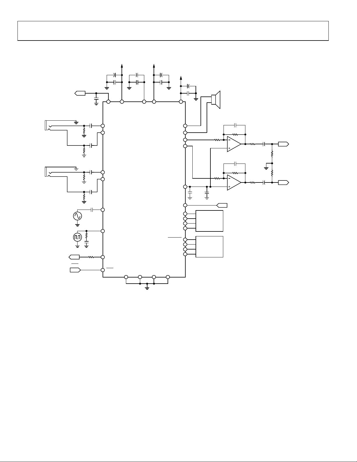
ADAU1381
A
SYSTEM BLOCK DIAGRAMS
MICBIAS
0.1µF
10µF
0.1µF
IOVDD
+
10µF
0.1µF
VDD1
+
10µF
0.1µF
AVDD2
+
47µF
+
8Ω
0.1µF
–
+
SPEAKER
OUT
DIFFERENTIAL INPUT
(LEFT)
49.9kΩ
49.9kΩ
DIFFERENTIAL INPUT
(RIGHT)
49.9kΩ
49.9kΩ
EXTERNAL
BEEP INPUT
EXTERNAL
MCLK SOURCE
MCKO
PDN
10µF
10µF
10µF
10µF
10µF
49.9Ω
2.2pF
49.9Ω
IOVDD
MICBIAS
LMIC/LMICN/MICD1
LMICP
ADAU1381
RMIC/RMICN/MICD2
RMICP
BEEP
MCKI
MCKO
PDN
THERM_PAD
(EXPOSED PAD)
AVDD1
DVDDOUT
DAC_SDATA/GPIO0
ADC_SDATA/GPIO1
BCLK/GPIO2
LRCLK/GPIO3
ADDR1/CLATCH
ADDR0/CDATA
DGND
AGND1
SPN
SPP
AOUTL
AOUTR
CM
GPIO
SDA/COUT
SCL/CCLK
AGND2
AVDD2
+
100nF 10µF
SERIAL
DATA
SYSTEM
CONTROLLER
10kΩ
10kΩ
GPIO
100pF
10kΩ
100pF
10kΩ
STEREO
HEADPHONE
AMPLIFIER
STEREO SINGLE-ENDED
HEADPHONE OUTP UT
LEFT_OUT
220µF
10Ω
+
10kΩ
10kΩ
220µF
10Ω
+
RIGHT_OUT
08313-021
Figure 23. System Block Diagram with Differential Inputs
Rev. B | Page 20 of 84
Page 21
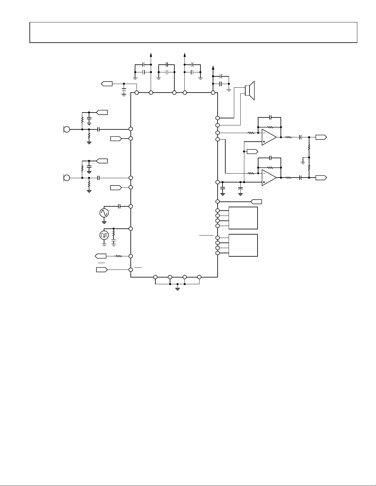
ADAU1381
A
A
A
MICBIAS
0.1µF
MICBIAS
49.9kΩ
49.9kΩ
EXTERNAL
BEEP INPUT
EXTERNAL
0.1µF
10µF
MICBIAS
0.1µF
10µF
MCKO
PDN
CM
CM
10µF
49.9Ω
2.2pF
49.9Ω
NALOG
MIC 1
NALOG
MIC 2
2kΩ
2kΩ
MCLK SOURCE
IOVDD
10µF
0.1µF
MICBIAS
LMIC/LMICN/MICD1
LMICP
10µF
+
0.1µF
IOVDD
ADAU1381
RMIC/RMICN/MICD2
RMICP
BEEP
MCKI
MCKO
PDN
THERM_PAD
(EXPOSED PAD)
VDD1
+
10µF
0.1µF
AVDD1
DVDDOUT
DAC_SDATA/GPIO0
ADC_SDATA/GPIO1
ADDR1/CLATCH
ADDR0/CDATA
DGND
AGND1
AVDD2
+
SPN
SPP
AOUTL
AOUTR
CM
GPIO
BCLK/GPIO2
LRCLK/GPIO3
SDA/COUT
SCL/CCLK
AGND2
47µF
0.1µF
AVDD2
+
–
+
10kΩ
10kΩ
+
100nF 10µF
SERIAL
DATA
SYSTEM
CONTROLLER
CM
GPIO
8Ω
SPEAKER
OUT
100pF
10kΩ
100pF
10kΩ
STEREO
HEADPHONE
AMPLIFIER
STEREO SINGLE-ENDED
HEADPHONE OUTP UT
LEFT_OUT
220µF
10Ω
+
10kΩ
10kΩ
220µF
10Ω
+
RIGHT_OUT
08313-022
Figure 24. System Block Diagram with Analog Microphone Inputs
Rev. B | Page 21 of 84
Page 22

ADAU1381
A
SINGLE-ENDED
STEREO INPUT
MCLK SOURCE
1kΩ
49.9kΩ
1kΩ
49.9kΩ
EXTERNAL
BEEP INPUT
EXTERNAL
MICBIAS
10µF
10µF
MCKO
PDN
0.1µF
CM
CM
10µF
49.9Ω
49.9Ω
2.2pF
IOVDD
10µF
0.1µF
MICBIAS
LMIC/LMICN/MICD1
LMICP
10µF
+
0.1µF
IOVDD
ADAU1381
RMIC/RMICN/MICD2
RMICP
BEEP
MCKI
MCKO
PDN
THERM_PAD
(EXPOSED PAD)
VDD1
+
10µF
0.1µF
AVDD1
DVDDOUT
DAC_SDATA/GPIO0
ADC_SDATA/GPIO1
ADDR1/CLATCH
ADDR0/CDATA
DGND
AGND1
AVDD2
+
SPN
SPP
AOUTL
AOUTR
CM
GPIO
BCLK/GPIO2
LRCLK/GPIO3
SDA/COUT
SCL/CCLK
AGND2
47µF
0.1µF
AVDD2
+
–
+
+
100nF 10µF
SERIAL
DATA
SYSTEM
CONTROLLER
10kΩ
CM
10kΩ
8Ω
SPEAKER
OUT
GPIO
100pF
10kΩ
100pF
10kΩ
STEREO
HEADPHONE
AMPLIFIER
STEREO SINGLE-ENDED
HEADPHONE OUTPUT
LEFT_OUT
220µF
10Ω
+
10kΩ
10kΩ
220µF
10Ω
+
RIGHT_OUT
08313-023
Figure 25. System Block Diagram with Single-Ended Stereo Line Inputs
Rev. B | Page 22 of 84
Page 23
ADAU1381
A
MICBIAS
0.1µF
BCLK OR MCLKO
STEREO DIGI T AL
MIC INPUT
1kΩ
10µF
EXTERNAL
BEEP INPUT
EXTERNAL
MCLK SOURCE
MCKO
49.9Ω
2.2pF
49.9Ω
PDN
IOVDD
10µF
0.1µF
MICBIAS
LMIC/LMICN/MICD1
LMICP
10µF
+
0.1µF
IOVDD
ADAU1381
RMIC/RMICN/MICD2
RMICP
BEEP
MCKI
MCKO
PDN
THERM_PAD
(EXPOSED PAD)
VDD1
+
10µF
0.1µF
AVDD1
DVDDOUT
DAC_SDATA/GPIO0
ADC_SDATA/GPIO1
ADDR1/CLATCH
ADDR0/CDATA
DGND
AGND1
AVDD2
+
SPN
SPP
AOUTL
AOUTR
CM
GPIO
BCLK/GPIO2
LRCLK/GPIO3
SDA/COUT
SCL/CCLK
AGND2
47µF
0.1µF
AVDD2
+
–
+
10kΩ
10kΩ
+
100nF 10µF
SERIAL
DATA
SYSTEM
CONTROLLER
8Ω
SPEAKER
OUT
GPIO
100pF
10kΩ
100pF
10kΩ
STEREO
HEADPHONE
AMPLIFIER
BCLK
STEREO SINGLE-ENDED
HEADPHONE OUTP UT
LEFT_OUT
220µF
10Ω
+
10kΩ
10kΩ
220µF
10Ω
+
RIGHT_OUT
08313-024
Figure 26. System Block Diagram with Stereo Digital Microphone Inputs
Rev. B | Page 23 of 84
Page 24

ADAU1381
THEORY OF OPERATION
The ADAU1381 is a low power audio codec with an integrated,
fixed-function audio processing sound engine. It is an all-in-one
package that offers high quality audio, low power, small size, and
many advanced features. The stereo ADC and stereo DAC each
have a dynamic range (DNR) performance of at least 96.5 dB and
a total harmonic distortion plus noise (THD + N) performance
of at least −90 dB. The serial data port is compatible with I
justified, right-justified, and TDM modes for interfacing to digital
audio data. The operating voltage range is 1.8 V to 3.65 V, with
an on-board regulator generating the internal digital supply voltage.
The record path includes very flexible input configurations that
can accept differential or single-ended analog microphone inputs
as well as two stereo digital microphone inputs. There is also a
beep input pin (BEEP) dedicated to analog beep signals that are
common in digital still camera applications. A microphone bias
pin that can power electrets-type microphones is also available.
Each input signal has its own programmable gain amplifier (PGA)
for input volume adjustment. An automatic level control (ALC)
is built into the sound engine to maintain a constant input recording volume.
The ADCs and DACs are high quality, 24-bit Σ- converters
that operate at selectable 64× or 128× oversampling rates. The
base sampling rate of the converters is set by the input clock rate
and can be further scaled with the converter control register
settings. The converters can operate at sampling frequencies
from 8 kHz to 96 kHz. The ADCs and DACs also include very
fine-step digital volume controls.
2
S, left-
The playback path allows input signals and DAC outputs to be
mixed into speaker and/or line outputs. The speaker driver is
capable of driving 400 mW into an 8 Ω load.
The fixed-function sound engine contains a digital audio
processing flow optimized for digital still camera stereo audio
processing. However, the flexibility offered by the built-in
sound engine allows this codec to be used for a wide variety of
low power applications. Signal processing blocks included in the
sound engine include the following:
• Wind noise detection and autofiltering
• Dual-band compression with programmable crossover,
compression curves, and timing
• Programmable multiband equalizer
• Configurable notch filter
• Enhanced stereo capture algorithm
• Automatic level control
• Digital volume control
• Multiplexers for signal routing
The ADAU1381 can generate its internal clocks from a wide
range of input clocks by using the on-board fractional PLL.
The PLL accepts inputs from 11 MHz to 20 MHz.
The ADAU1381 is provided in a small, 32-lead, 5 mm × 5 mm
lead frame chip scale package (LFCSP) with an exposed bottom
pad, or a 30-ball (6 × 5 bump), 3.4 mm × 2.64 mm wafer level
chip scale package (WLCSP).
Rev. B | Page 24 of 84
Page 25
ADAU1381
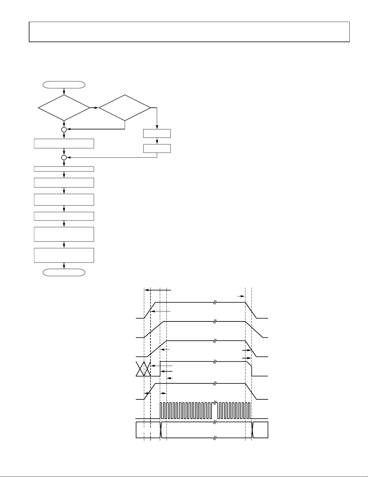
STARTUP, INITIALIZATION, AND POWER
This section details the procedure for setting up the ADAU1381
properly. Figure 27 provides an overview of how to initialize the IC.
START
ARE AVDD1 AND AVDD2
SUPPLIED SEPARATELY?
NO
SUPPLY POWER TO AVDD1/AVDD2
PINS SIMULTANEOUSLY
CAN AVDD1 AND AVDD2
BE SIMULTANEOUSLY
SUPPLIED?
YES
NOYES
SUPPLY POWER
TO AVDD1
SUPPLY POWER
TO AVDD2
POWER-UP SEQUENCE
If AVDD1 and AVDD2 are from the same supply, they can
power up simultaneously. If AVDD1 and AVDD2 are from
separate supplies, then AVDD1 should be powered up first.
IOVDD should be applied simultaneously with AVDD1, if
possible.
The ADAU1381 uses a power-on reset (POR) circuit to reset the
registers upon power-up. The POR monitors the DVDDOUT
pin and generates a reset signal whenever power is applied to
the chip. During the reset, the ADAU1381 is set to the default
values documented in the register map (see the Control Register
Map section).
SUPPLY POWER TO I OVDD
WAIT 14ms FOR POWER-ON RESET
AND INITIALIZATION ROM BOOT
CONFIGURE CLOCK GENERATION
REGISTER 16384 (0x4000)
AND REGISTER 16386 (0x4002)
WAIT FOR PLL LOCK
(2.4ms TO 3.5ms)
ENABLE DIG ITAL POW E R T O
FUNCTIONA L SUBSY ST EMS
REGISTER 16512 (0x4080)
AND REGISTER 16513 (0x4081)
SET UP SOUND ENGINE REG ISTERS
FOR CUSTOMI ZED SIGNAL PATH
(INCLUDING VOLUME, SAMPLE RATES,
FILTER COEFFICIENTS)
INITIALIZATION
COMPLETE
Figure 27. Initialization Sequence
AVDD1
AVDD2
DVDDOUT
POWER-UP
(INTERNAL
SIGNAL)
IOVDD
14ms
The POR is also used to prevent clicks and pops on the speaker
driver output. The power-up sequencing and timing involved is
described in Figure 28 in this section, and in Figure 36 and
Figure 37 of the Speaker Output section.
A self-boot ROM initializes the memories after the POR has
completed. When the self-boot sequence is complete, the control
registers are accessible via the I
then be configured as required for the application. Typically,
with a 10 F capacitor on AVDD1, the power supply ramp-up,
POR, and self-boot combined take approximately 14 ms.
08313-025
MAIN SUPPLY ENABLED
MAIN SUPPLY DISABLED
1.5V
1.5V
1.35V
ACTIVE
POR ACTIVATES
POR COMPLETE/SELF-BOOT INITIATES
SELF-BOOT COMPLETE/MEMORY
IS ACCESSIBLE
0.95V
POR
2
C/SPI control port and should
INTERNAL MCLK
(NOT TO SCALE)
INPUT/OUTPUT
PINS
Figure 28. Power-Up and Power-Down Sequence Timing Diagram
ACTIVE
HIGH-ZHIGH-Z
08313-026
Rev. B | Page 25 of 84
Page 26
ADAU1381
CLOCK GENERATION AND MANAGEMENT
The ADAU1381 uses a flexible clocking scheme that enables the
use of many different input clock rates. The PLL can be bypassed
or used, resulting in two different approaches to clock management. For more information about clocking schemes, PLL
configuration, and sampling rates, see the Clocking and
Sampling Rates section.
Case 1: PLL Is Bypassed
If the PLL is bypassed, the core clock is derived directly from
the master clock (MCLK) input. The rate of this clock must be
set properly in Register 16384 (0x4000), clock control, Bits[2:1],
input master clock frequency. When the PLL is bypassed,
supported external clock rates are 256 × f
and 1024 × f
of the chip is off until Register 16384 (0x4000), clock control,
Bit 0, core clock enable, is set to 1.
, where fS is the base sampling rate. The core clock
S
Case 2: PLL Is Used
The core clock to the entire chip is off during the PLL lock
acquisition period. The user can poll the lock bit to determine
when the PLL has locked. After lock is acquired, the ADAU1381
can be started by setting Register 16384 (0x4000), clock control,
Bit 0, core clock enable, to 1.This bit enables the core clock to all
the internal functional blocks of the ADAU1381.
PLL Lock Acquisition
During the lock acquisition period, only Register 16384 (0x4000),
clock control, and Register 16386 (0x4002), PLL control, are
accessible through the control port. Reading from or writing to
any other address is prohibited until Register 16384 (0x4000),
clock control, Bit 0, core clock enable, and Register 16386 (0x4002),
PLL control, Bit 1, PLL lock, are set to 1.
Register 16386 (0x4002), PLL control, is a 48-bit register for which
all bits must be written with a single continuous write to the
control port.
The PLL lock time is dependent on the MCLK rate. Typical lock
times are provided in Tab le 1 1.
Table 11. PLL Lock Time
PLL Mode MCLK Frequency Lock Time (Typical)
Fractional 12 MHz 3.0 ms
Integer 12.288 MHz 2.96 ms
Fractional 13 MHz 2.4 ms
Fractional 14.4 MHz 2.4 ms
Fractional 19.2 MHz 2.98 ms
Fractional 19.68 MHz 2.98 ms
Fractional 19.8 MHz 2.98 ms
, 512 × fS, 768 × fS,
S
ENABLING DIGITAL POWER TO FUNCTIONAL SUBSYSTEMS
To power subsystems in the device, they must be enabled using
Register 16512 (0x4080), Digital Power-Down 0, and Register
16513 (0x4081), Digital Power-Down 1. The exact settings depend
on the application. However, to proceed with the initialization
sequence and access the RAMs and registers of the ADAU1381,
Register 16512 (0x4080), Digital Power-Down 0, Bit 6, memory
controller, and Bit 0, sound engine, must be enabled.
SETTING UP THE SOUND ENGINE
After the PLL has locked, the ADAU1381 is in an operational
state, and the control port can be used to configure the sound
engine. For more information, see the Sound Engine section.
POWER REDUCTION MODES
Sections of the ADAU1381 chip can be turned on and off as
needed to reduce power consumption. These include the ADCs,
the DACs, and the PLL.
In addition, some functions can be set in the registers to operate
in power saving, normal, or enhanced performance operation.
See the respective portions of the General-Purpose Input/Outputs
section for more information.
Each digital filter of the ADCs and DACs can be set to a 64× or
128× (default) oversampling ratio. Setting the oversampling ratio
to 64× lowers power consumption with a minimal impact on
performance. See the Typical Performance Characteristics section
and the Typical Power Management Measureme nts section for
specifications and graphs of the filters.
Detailed information regarding individual power reduction control
registers can be found in the Control Register Map section of this
document.
Power-Down Pin (
The power-down pin provides a simple hardware-based
method for initiating low power mode without requiring access
via the control port. When the
potential as ground, the internal digital regulator is disabled
and the device ceases to function, with power consumption
dropping to a very low level. The common-mode voltage sinks,
and all internal memories and registers lose their contents.
When the
AVDD1, the device reinitializes in its default state, as described
in the section. Power-Up Sequence
PDN
PDN
)
PDN
pin is lowered to the same
pin is raised back to the same potential as
POWER-DOWN SEQUENCE
When powering down the device, the IOVDD, AVDD1, and
AVDD2 supplies should be disabled at the same time, if possible,
but only after the analog and speaker outputs have been muted. If
the supplies cannot be disabled simultaneously, the preferred
sequence is IOVDD first, AVDD2 second, and AVDD1 last.
Rev. B | Page 26 of 84
Page 27

ADAU1381
CLOCKING AND SAMPLING RATES
SOUND ENGINE
FRAME RATE
SOUND
ENGINE
ADCs DACs
SERIAL DATA
INPUT/OUTPUT
PORTS
BCLK/GPIO2
LRCLK/GPIO3
DC_SDATA/GPIO1
DAC_SDATA/GPIO0
08313-027
MCKI
f/X
INPUT DIVIDE
1, 2, 3, 4
PLL CONTRO L CLO CK CO NTROL
f × (R + N/M)
INTEGER, NUM E RATOR,
DENOMINATOR
AUTOMATICALLY SET TO 1024 ×
WHEN PLL CL OCK SOURCE SEL E CTED
INPUT MASTER
CLOCK FREQUENCY
256 ×
f
, 512 × fS,
S
768 ×
f
, 1024 × f
S
Figure 29. Clock Routing Diagram
f
/
S
0.5, 1, 1. 5 , 2, 3, 4, 6
CONVERTER
CORE
CLOCK
S
f
S
SAMPLING RATE
f
/
S
0.5, 1, 1. 5 , 2, 3, 4, 6
SERIAL PO RT
SAMPLING RATE
f
/
S
0.5, 1, 1. 5 , 2, 3, 4, 6
CORE CLOCK
The core clock divider generates a core clock either from the
PLL or directly from MCLK and can be set in Register 16384
(0x4000), clock control.
The core clock is always in 256 × f
quencies must correspond to a value listed in Tab le 1 2 , where f
is the base sampling frequency. PLL outputs are always in 1024
× f
mode, and the clock control register automatically sets the
S
core clock divider to f/4 when using the PLL.
Table 12. Core Clock Frequency Dividers
Input Clock Rate Core Clock Divider Core Clock
256 × fS f/1 256 × fS
f/2
512 × f
S
768 × fS f/3
1024 × f
f/4
S
Clocks for the converters, the serial ports, and the sound engine are
derived from the core clock. The core clock can be derived directly
from MCLK, or it can be generated by the PLL. Register 16384
(0x4000), clock control, Bit 3, clock source select, determines
the clock source.
Bits[2:1], input master clock frequency, should be set according
to the expected input clock rate selected by Bit 3, clock source
select. The clock source select value also determines the core
clock rate and the base sampling frequency, f
mode. Direct MCLK fre-
S
.
S
S
For example, if the input to Bit 3 = 49.152 MHz (from PLL),
then Bits[2:1] = 1024 × f
= 49.152 MHz/1024 = 48 kHz
f
S
; therefore,
S
Table 13. Clock Control Register (Register 16384, 0x4000)
Bits Bit Name
3 Clock source select
Settings
0: direct from MCKI pin (default)
1: PLL clock
[2:1]
Input master clock
frequency
0 Core clock enable
00: 256 × f
01: 512 × f
10: 768 × f
11: 1024 × f
0: core clock disabled (default)
(default)
S
S
S
S
1: core clock enabled
SAMPLING RATES
The ADCs, DACs, and serial port share a common sampling
rate that is set in Register 16407 (0x4017), Converter Control 0.
Bits[2:0], converter sampling rate, set the sampling rate as a ratio of
the base sampling frequency. The sound engine sampling rate is
set in Register 16619 (0x40EB), sound engine frame rate, Bits[3:0],
sound engine frame rate, and the serial port sampling rate is set
in Register 16632 (0x40F8), serial port sampling rate, Bits[2:0],
serial port control sampling rate.
It is strongly recommended that the sampling rates for the
converters, serial ports, and sound engine be set to the same
value, unless appropriate compensation filtering is done within
the sound engine.
Rev. B | Page 27 of 84
Page 28

ADAU1381
Tabl e 14 and Ta ble 1 5 list the sampling rate divisions for
common base sampling rates.
Table 14. Base Sampling Rate Divisions for f
= 48 kHz
S
Base Sampling
Frequency Sampling Rate Scaling Sampling Rate
fS = 48 kHz fS/1 48 kHz
f
f
f
f
f
f
/6 8 kHz
S
/4 12 kHz
S
/3 16 kHz
S
/2 24 kHz
S
/1.5 32 kHz
S
/0.5 96 kHz
S
Table 15. Base Sampling Rate Divisions for fS = 44.1 kHz
Base Sampling
Frequency Sampling Rate Scaling Sampling Rate
fS = 44.1 kHz fS/1 44.1 kHz
f
f
f
f
f
f
/6 7.35 kHz
S
/4 11.025 kHz
S
/3 14.7 kHz
S
/2 22.05 kHz
S
/1.5 29.4 kHz
S
/0.5 88.2 kHz
S
PLL
The PLL uses the MCLK as a reference to generate the core
clock. PLL settings are set in Register 16386 (0x4002), PLL
control. Depending on the MCLK frequency, the PLL must be
set for either integer or fractional mode. The PLL can accept
input frequencies in the range of 11 MHz to 20 MHz.
All six bytes in the PLL control register must be written with a
single continuous write to the control port.
TO PLL
MCKI
÷ X
× (R + N/M)
Figure 30. PLL Block Diagram
Integer Mode
Integer mode is used when the MCLK is an integer (R) multiple
of the PLL output (1024 × f
).
S
CLOCK DIVIDE R
08313-028
Fractional Mode
Fractional mode is used when the MCLK is a fractional
(R + (N/M)) multiple of the PLL output.
For example, if MCLK = 12 MHz and f
= 48 kHz, then
S
PLL Required Output = 1024 × 48 kHz = 49.152 MHz
R + (N/M) = 49.152 MHz/12 MHz = 4 + (12/125)
Common fractional PLL parameter settings for 44.1 kHz and
48 kHz sampling rates can be found in Tab le 16 and Ta ble 17 .
Table 16. Fractional PLL Parameter Settings for f
MCLK
Input
(MHz)
Input
Divider
(X)
Integer
(R)
Denominator
(M)
= 44.1 kHz1
S
Numerator
(N)
12 1 3 625 477
13 1 3 8125 3849
14.4 2 6 125
19.2 2 4 125
19.68 2 4 1025
34
88
604
19.8 2 4 1375 772
1
Desired core clock = 11.2896 MHz, PLL output = 45.1584 MHz.
Table 17. Fractional PLL Parameter Settings for fS = 48 kHz1
MCLK
Input
(MHz)
Input
Divider
(X)
Integer
(R)
Denominator
(M)
Numerator
(N)
12 1 4 125 12
13 1 3 1625 1269
14.4 2 6 75
62
19.2 2 5 25 3
19.68 2 4 205
204
19.8 2 4 825 796
1
Desired core clock = 12.288 MHz, PLL output = 49.152 MHz.
The PLL outputs a clock in the range of 41 MHz to 54 MHz,
which should be taken into account when calculating PLL
values and MCLK frequencies.
For example, if MCLK = 12.288 MHz and f
= 48 kHz, then
S
PLL Required Output = 1024 × 48 kHz = 49.152 MHz
R = 49.152 MHz/12.288 MHz = 4
In integer mode, the values set for N and M are ignored.
Rev. B | Page 28 of 84
Page 29

ADAU1381
The ADC and DAC sampling rate can be set in Register 16407
(0x4017), Converter Control 0, Bits[2:0], converter sampling
rate. The sound engine sampling rate and serial port sampling
rate are similarly set in Register 16619 (0x40EB), sound engine
frame rate, Bits[3:0], sound engine frame rate, and Register
16632 (0x40F8), serial port sampling rate, Bits[2:0], serial port
control sampling rate, respectively.
Tabl e 18 and Ta ble 1 9 depict example sampling rate settings.
The (1 × 256) case is the base sampling rate.
Table 18. Sampling Rates for 256 × 48 kHz Core Clock
Core Clock Sampling Rate Divider Sampling Rate
12.288 MHz (1 × 256) 48 kHz
(6 × 256) 8 kHz
(4 × 256) 12 kHz
(3 × 256) 16 kHz
(2 × 256) 24 kHz
(1.5 × 256) 32 kHz
(0.5 × 256) 96 kHz
Table 19. Sampling Rates for 256 × 44.1 kHz Core Clock
Core Clock Sampling Rate Divider Sampling Rate
11.2896 MHz (1 × 256) 44.1 kHz
(6 × 256) 7.35 kHz
(4 × 256) 11.025 kHz
(3 × 256) 14.7 kHz
(2 × 256) 22.05 kHz
(1.5 × 256) 29.4 kHz
(0.5 × 256) 88.2 kHz
Rev. B | Page 29 of 84
Page 30

ADAU1381
RECORD SIGNAL PATH
BEEP
LMIC/LMICN/
MICD1
PGA
Analog Beep Input
The BEEP pin is used for mono single-ended signals, such as a
beep warning. This signal bypasses the ADCs and the sound
engine and is mixed directly into any of the analog outputs.
LMICP
RMIC/RMICN/
MICD2
RMICP
PGA
CM
PGA
CM
LEFT
ADC
RIGHT
ADC
DECIMATORS
8313-029
Figure 31. Record Signal Path Diagram
INPUT SIGNAL PATH
The ADAU1381 can be configured for three types of microphone
inputs: single-ended, differential, or digital. The LMIC/LMICN/
MICD1 and RMIC/RMICN/MICD2 pins encompass all of these
configurations. LMICP and RMICP are used only during
differential configurations (see Figure 31, the record signal path
diagram).
Each analog input has individual gain controls (boost or cut). These
signals are routed to their respective right or left channel ADC.
Analog Microphone Inputs
For differential inputs, RMICN and RMICP denote the negative
and positive input for the right channel, respectively. LMICN
and LMICP denote the negative and positive input for the left
channel, respectively.
LMIC and RMIC inputs are single-ended line inputs. Together,
they can be used as a stereo single-ended input.
Digital Microphone Inputs
When a digital PDM microphone connected to the MICD1 or
MICD2 pin is used, Register 16392 (0x4008), digital microphone
and analog beep control, must be set appropriately to enable the
microphone input of choice. The MCKO output clock provides
the clock for the microphone and must be set accordingly in
Register 16384 (0x4000), clock control, depending on the
streaming PDM rate of the microphone.
A BEEP pin input ca
n also be amplified or muted by a PGA, up
to 32 dB in Register 16392 (0x4008), digital microphone and an
beep control. The beep input must be enabled in Register 16
400
(0x4010), microphone bias control and beep enable.
Microphone Bias
The MICBIAS pin provides a voltage reference for electret
microphones. Register 16400 (0x4010), microphone bias
control and beep enable, sets the operation mode of this pin.
Example Configurations
CM
CM
TO DECIMATORS
PGA
TO DECIMATORS
PGA
TO LEFT
ADC
PGA
TO RIGHT
ADC
PGA
8313-030
8313-031
LMIC/LMICN/
MICD1
LMICP
RMIC/RMICN/
MICD2
RMICP
Figure 32. Stereo Digital Microphone Input Configuration
LMIC/LMICN/
MICD1
LMICP
CM
RMIC/RMICN/
MICD2
RMICP
CM
Figure 33. Single-Ended Input Configuration
alog
The digital microphone signal bypasses the ADCs and is routed
directly into the decimation filters. The digital microphone and
ADCs share these decimation filters; therefore, both cannot be
used simultaneously.
Rev. B | Page 30 of 84
Page 31

ADAU1381
LMIC/LMICN/
MICD1
LMICP
CM
RMIC/RMICN/
MICD2
RMICP
CM
Figure 34. Differential Input Configuration
PGA
PGA
TO LEFT
ADC
TO RIGHT
ADC
8313-032
ANALOG-TO-DIGITAL CONVERTERS
The ADAU1381 uses two 24-bit Σ- analog-to-digital converters
(ADCs) with selectable oversampling rates of either 64× or 128×.
The full-scale input to the ADCs depends on AVDD1. At 3.3 V,
the full-scale input level is 1.0 V rms. Inputs greater than the
full-scale value result in clipping and distortion.
Digital ADC Volu
me Control
The ADC output (digital input) volume can be adjusted in
Register 16410 (0x401A), left ADC attenuator, Bits[7:0], left ADC
digital attenuator, for the left channel digital volume control and
in Register 16411 (0x401B), right ADC attenuator, Bits[7
ADC digital attenuator, for right channel digital volum
:0], right
e control.
High-Pass Filter
A high-pass filter is used in the ADC path to remove dc offsets
and can be selected in Register 16409 (0x4019), ADC control,
Bit 5, high-pass filter select, where it can be enabled or disabled.
DIGITAL DUAL-BAND AUTOMATIC LEVEL CONTROL (ALC)
The ADAU1381 includes an automatic level control (ALC). The
ALC adjusts the input gain continuously for a varying input signal
as dictated by the user-defined ALC settings. This allows the input
recording level to remain constant. Although this functionality
relates mainly to the record signal path, it is implemented digitally
in the sound engine.
Rev. B | Page 31 of 84
Page 32

ADAU1381
K
A
R
PLAYBACK SIGNAL PATH
LEFT P LAYBAC
MIXER
MONO
PLAYBACK
MIXER
RIGHT PLAYBACK
MIXER
BEEP FROM
RECORD PG
LEFT
DAC
PLAYBACK
BEEP GAIN
PLAYBACK
BEEP GAIN
RIGHT
DAC
LEFT
RIGHT
MONO
PLAYBACK
BEEP GAIN
Figure 35. Playback Signal Path Diagram
OUTPUT SIGNAL PATHS
The outputs of the ADAU1381 include a left and right line output
and speaker driver. The beep input signal can be mixed into any
of these outputs, with separate gain control for each path.
DIGITAL-TO-ANALOG CONVERTERS
The ADAU1381 uses two 24-bit Σ- digital-to-analog converters
(DACs) with selectable oversampling rates of 64× or 128×. The
full-scale output of the DACs depends on AVDD1. At 3.3 V, the
full-scale output level is 1.0 V rms.
Digital DAC Volume Control
The DAC output (digital output) volume can be adjusted in
Register 16427 (0x402B), left DAC attenuator, for the left channel
digital volume control and in Register 16428 (0x402C), right
DAC attenuator, for the right channel digital volume control.
De-Emphasis Filter
A de-emphasis filter is used in the DAC path to remove high
frequency noise in an FM system. This filter can be enabled or
disabled in Register 16426 (0x402A), DAC control.
LINE OUTPUTS
The AOUTL and AOUTR pins are the left and right line outputs,
respectively. Both outputs have a line output amplifier that can
be set in the control registers.
The left playback mixer is dedicated to the AOUTL output. This
mixer mixes the left DAC and the beep signal.
Similarly, the right playback mixer mixes the right DAC and the
beep input and is dedicated to the AOUTR output.
SPEAKER OUTPUT
The SPP and SPN pins are the positive and negative speaker
outputs, respectively. Each output has a speaker driver.
LINE OUT
AMPLIFIER
MONO
OUTPUT
GAIN
–1
MONO OUT P UT
INVERTER
LINE OUT
AMPLIFIER
AOUTL
SPP
SPN
AOUTR
beep signal. The mixer can be controlled in Register 16415
(0x401F), playback mono mixer control.
The drivers are low noise, Class AB mono amplifiers designed to
drive 8 , 400 mW speakers. The output is differential and does
not require external capacitors. The gain settings for the speaker
drivers can be set in Register 16423 (0x4027), playback speaker
output control. In this register, the drivers can be set for any of
the four gain settings: 0 dB, 2 dB, 4 dB, or 6 dB. Additionally,
the speaker driver can be muted or powered down completely.
For pop and click suppression, an internal precharge sequence with
output gating/enabling occurs after the mono driver is enabled.
08313-033
The sequence lasts for 8 ms, and then the internal mute signal
rising edge occurs (see Figure 36 for the power-up sequence
timing diagram).
The power-down sequence is essentially the reverse of the startup sequence, as depicted in Figure 37.
SPEAKE
OUTPUT
ENABLE
MONO
OUTPUT
MUTE
SPP
SPN
I
AVDD2
DAC
BEEP
SPEAKER
OUTPUT
ENABLE
MONO
OUTPUT
MUTE
SPP
SPN
I
AVDD2
DAC
BEEP
4ms 4ms
V
HIGH-Z
HIGH-Z
<1µA 1.1mA 2.3mA
DAC VOLUME MUTED
BEEP VOLUME MUTED
CM
V
CM
2.3mA + SIGNAL
CURRENT
DAC VOLUME
INCREASES
BEEP VOLUME
INCREASES
Figure 36. Speaker Driver Power-Up Sequence
V
CM
V
CM
2.3mA + SIGNAL
CURRENT
DAC VOLUME
DECREASES
BEEP VOLUME
DECREASES
DAC VOLUME MUTED
BEEP VOLUME MUTED
Figure 37. Speaker Driver Power-Down Sequence
4ms4ms
HIGH-Z
HIGH-Z
<1µA1.1mA2.3mA
8313-034
8313-035
The speaker outputs are derived from the mono playback mixer,
which sums the right and left DAC outputs and mixes with the
Rev. B | Page 32 of 84
Page 33

ADAU1381
CONTROL PORTS
The ADAU1381 can operate in one of two control modes: I2C
control or SPI control.
The ADAU1381 has both a 4-wire SPI control port and a 2-wire
2
I
C bus control port. Each can be used to set the registers. The
part defaults to I
by pulling the
2
C mode but can be put into SPI control mode
CLATCH
pin low three times.
The control port is capable of full read/write operation for all
addressable registers. Most sound engine processing parameters
are controlled by writing new values to the sound engine parameter
register using the control port. Other functions, such as mute,
input/output mode control, and analog signal paths, can be
programmed by writing to the appropriate registers.
All addresses can be accessed in either a single-address mode or
a burst mode. The first byte (Byte 0) of a control port write contains
the 7-bit chip address plus the R/
W
bit. The next two bytes (Byte 1
and Byte 2) together form the subaddress of the register location
within the ADAU1381. All subsequent bytes (starting with Byte 3)
contain the data, such as control port data, register data, or sound
engine parameter data. The number of bytes per word depends
on the type of data that is being written. The exact formats for
specific types of writes and reads are shown in to
Figure 43
.
Figure 40
The ADAU1381 has several mechanisms for updating sound
engine parameters in real time without causing pops or clicks.
The control port pins are multifunctional, depending on the
mode in which the part is operating. Ta b le 2 0 details these
multiple functions.
Table 20. Control Port Pin Functions
Pin I2C Mode SPI Mode
SCL/CCLK SCL—input CCLK—input
SDA/COUT SDA—open-collector output COUT—output
ADDR1/CLATCH
ADDR0/CDATA I2C Address Bit 0—input CDATA—input
2
I
C Address Bit 1—input
CLATCH
—input
I2C PORT
The ADAU1381 supports a 2-wire serial (I2C-compatible)
microprocessor bus driving multiple peripherals. Two pins,
serial data (SDA) and serial clock (SCL), carry information
between the ADAU1381 and the system I
2
In I
C mode, the ADAU1381 is always a slave on the bus, meaning
it cannot initiate a data transfer. Each slave device is recognized by
a unique address. The address byte format is shown in Tabl e 21 .
The address resides in the first seven bits of the I
LSB of this byte sets either a read or write operation. Logic 1
corresponds to a read operation, and Logic 0 corresponds to a
write operation. The full byte addresses, including the pin settings
W
and R/
bit, are shown in . Tabl e 2 2
2
C master controller.
2
C write. The
Burst mode addressing, where the subaddresses are automatically incremented at word boundaries, can be used for writing
large amounts of data to contiguous memory locations. This
increment happens automatically after a single-word write unless a
stop condition is encountered. The registers in the ADAU1381
range in width from one to six bytes; therefore, the auto-increment
feature knows the mapping between subaddresses and the word
length of the destination register. A data transfer is always
terminated by a stop condition.
Both SDA and SCL should have 2.0 kΩ pull-up resistors on the
lines connected to them. The voltage on these signal lines should
not be more than AVDD1.
Table 21. I
Bit 0 Bit 1 Bit 2 Bit 3 Bit 4 Bit 5 Bit 6 Bit 7
0 1 1 1 0 ADDR1 ADDR0
2
C Address Byte Format
R/W
Table 22. I2C Addresses
ADDR1 ADDR0
0 0 0 0x70
0 0 1 0x71
0 1 0 0x72
0 1 1 0x73
1 0 0 0x74
1 0 1 0x75
1 1 0 0x76
1 1 1 0x77
R/W
Slave Address
Addressing
Initially, each device on the I2C bus is in an idle state and
monitoring the SDA and SCL lines for a start condition and
the proper address. The I
2
C master initiates a data transfer by
establishing a start condition, defined by a high-to-low transition
on SDA while SCL remains high. This indicates that an address or
an address and data stream follow. All devices on the bus respond
to the start condition and shift the next eight bits (the 7-bit
address plus the R/
W
bit), MSB first. The device that recognizes
the transmitted address responds by pulling the data line low
during the ninth clock pulse. This ninth bit is known as an
acknowledge bit. All other devices withdraw from the bus at
this point and return to the idle condition.
W
The R/
bit determines the direction of the data. A Logic 0 on the
LSB of the first byte means the master writes information to the
peripheral, whereas a Logic 1 means the master reads information
from the peripheral after writing the subaddress and repeating
the start address. A data transfer takes place until a stop condition
is encountered. A stop condition occurs when SDA transitions
from low to high while SCL is held high. shows the
timing of an I
2
C write, and shows an I2C read.
Figure 39
Figure 38
Rev. B | Page 33 of 84
Page 34

ADAU1381
(
(
(
(
Stop and start conditions can be detected at any stage during
the data transfer. If these conditions are asserted out of sequence
with normal read and write operations, the ADAU1381
immediately jumps to the idle condition. During a given SCL
high period, the user should issue only one start condition, one
stop condition, or a single stop condition followed by a single
start condition. If an invalid subaddress is issued by the user,
the ADAU1381 does not issue an acknowledge and returns to
the idle condition. If the user exceeds the highest subaddress while
SCL
111
SDA
START BY
MASTER
SCL
(CONTINUED)
SDA
(CONTINUED)
0
CHIP ADDRESS BYTE
SUBADDRESS BYTE 2
0
FRAME 1
FRAME 3
Figure 38. I
R/W
ADDR0ADDR1
ACKNOWLEDGE
BY ADAU1381
ACKNOWLEDGE
BY ADAU1381
2
C Write to ADAU1381 Clocking
in auto-increment mode, one of two actions is taken. In read mode,
the ADAU1381 outputs the highest subaddress register contents
until the master device issues a no acknowledge, indicating the
end of a read. A no-acknowledge condition is where the SDA
line is not pulled low on the ninth clock pulse on SCL. If the
highest subaddress location is reached while in write mode, the
data for the invalid byte is not loaded into any subaddress register,
a no acknowledge is issued by the ADAU1381, and the part returns
to the idle condition.
ACKNOWLEDGE
BY ADAU1381
FRAME 2
SUBADDRESS BYTE 1
FRAME 4
DATA BYTE 1
ACKNOWLEDGE
BY ADAU1381
STOP BY
MASTER
8313-036
CONTINUED)
CONTINUED)
CONTINUED)
CONTINUED)
SCL
SDA
START BY
MASTER
SCL
SDA
SCL
SDA
0111
FRAME 1
CHIP ADDRESS BYTE
FRAME 3
SUBADDRESS BYTE 2
FRAME 5
READ DATA BYTE 1
0
Figure 39. I
R/W
ADDR0ADDR1
ACKNOWLEDGE
BY ADAU1381
ACKNOWLEDGE
BY ADAU1381
ACKNOWLEDGE
BY ADAU1381
2
C Read from ADAU1381 Clocking
FRAME 2
SUBADDRESS BYTE 1
0111
REPEATED
START BY MASTER
READ DATA BYTE 2
FRAME 4
CHIP ADDRESS BYTE
FRAME 6
ACKNOWLEDGE
BY ADAU1381
0
ACKNOWLEDGE
BY ADAU1381
ACKNOWLEDGE
BY MASTER
R/W
ADDR0ADDR1
STOP BY
MASTER
08313-037
Rev. B | Page 34 of 84
Page 35

ADAU1381
I2C Read and Write Operations
Figure 40 shows the timing of a single-word write operation.
Every ninth clock pulse, the ADAU1381 issues an acknowledge
by pulling SDA low.
Figure 41 shows the timing of a burst mode write sequence.
This figure shows an example where the target destination
registers are two bytes. The ADAU1381 knows to increment its
subaddress register every two bytes because the requested
subaddress corresponds to a register or memory area with a
2-byte word length.
The timing of a single-word read operation is shown in Figure 42.
Note that the first R/
W
bit is 0, indicating a write operation. This is
because the subaddress still needs to be written to set up the
internal address. After the ADAU1381 acknowledges the receipt
of the subaddress, the master must issue a repeated start command
followed by the chip address byte with the R/
W
bit set to 1 (read).
This causes the ADAU1381 SDA to reverse and begin driving
data back to the master. The master then responds every ninth
pulse with an acknowledge pulse to the ADAU1381.
Figure 43 shows the timing of a burst mode read sequence. This
figure shows an example where the target read registers are two
bytes. The ADAU1381 increments its subaddress every two bytes
because the requested subaddress corresponds to a register or
memory area with word lengths of two bytes. Other address
ranges may have a variety of word lengths ranging from one to
five bytes. The ADAU1381 always decodes the subaddress and
sets the auto-increment circuit so that the address increments
after the appropriate number of bytes.
CHIP ADDRESS,
S
R/W = 0
S = START BI T, P = STOP BIT, AS = ACKNOWLEDGE BY SLAVE.
SHOWS A ONE-W O RD W RI TE, WHERE EACH W O RD HAS N BYTE S.
AS
SUBADDRESS,
HIGH BYTE
SUBADDRESS,
AS AS AS AS ... AS P
LOW BYTE
Figure 40. Single-Word I
DATA
BYTE 1
2
C Write Sequence
DATA
BYTE 2
DATA
BYTE N
08313-038
CHIP
S AS AS ASASASASAS ASAS
ADDRESS,
R/W = 0
S = START BI T, P = STOP BIT, AS = ACKNOWLEDGE BY SLAVE.
SHOWS AN N-WORD WRITE, WHERE EACH WORD HAS TWO BY TES. (OTHER WORD LE NGTHS ARE POSS IBLE, RANGING FROM ONE TO FIVE BYTES.)
SUBADDRESS,
HIGH BYTE
SUBADDRESS,
LOW BYTE
DATA-WO RD 1 ,
BYTE 1
DATA-WO RD 1 ,
BYTE 2
Figure 41. Burst Mode I
DATA-WO RD 2,
BYTE 1
2
C Write Sequence
DATA-WO RD 2 ,
BYTE 2
...
DATA-WO RD N ,
BYTE 1
DATA-WO RD N ,
BYTE 2
P
8313-039
CHIP ADDRESS,
S
R/W = 0
S = START BIT, P = ST OP BIT, AM = ACKNOWLEDGE BY M AS TER, AS = ACKNOWLEDGE BY SLAVE.
SHOWS A ONE- WORD READ, WHERE EACH WORD HAS N BYTES.
SUBADDRESS,
HIGH BYT E
SUBADDRESS,
LOW BYTE
Figure 42. Single-Word I
CHIP ADDRESS,
R/W = 1
2
C Read Sequence
DATA
BYTE 1
DATA
BYTE 2
DATA
...
AMAMAS AMAS SASAS
BYTE N
P
08313-040
CHIP
SAS AS AS AS AMAM AMAM
ADDRESS,
R/W = 0
SUBADDRESS,
HIGH BYTE
SUBADDRESS,
LOW BYTE
S
CHIP
ADDRESS,
R/W = 1
...
P
DATA-WORD 1,
BYTE 1
S = START BIT, P = ST OP BIT, AM = ACKNOWLEDGE BY M AS TER, AS = ACKNOWLEDGE BY SLAVE.
SHOWS AN N-WORD READ, WHERE E ACH W ORD HAS TWO BY TES. (OTHER WORD LENGTHS ARE POS S IBLE, RANGING FROM O NE TO FI V E BY TES.)
Figure 43. Burst Mode I
2
C Read Sequence
DATA-WO RD 1 ,
BYTE 2
DATA-WO RD N,
BYTE 1
DATA-WO RD N,
BYTE 2
08313-041
Rev. B | Page 35 of 84
Page 36

ADAU1381
SPI PORT
By default, the ADAU1381 is in I2C mode, but can be put into SPI
control mode by pulling
CLATCH
uses a 4-wire interface, consisting of
and COUT signals, and is always a slave port. The
goes low at the beginning of a transaction and high at the end of
a transaction. The CCLK signal latches CDATA on a low-to-high
transition. COUT data is shifted out of the ADAU1381 on the
falling edge of CCLK and should be clocked into a receiving
device, such as a microcontroller, on the CCLK rising edge. The
CDATA signal carries the serial input data, and the COUT signal is
the serial output data. The COUT signal remains three-stated until
a read operation is requested. This allows other SPI-compatible
peripherals to share the same readback line. All SPI transactions
have the same basic format shown in . A timing diagram
is shown in . All data should be written MSB first. The
Figure 4
ADAU1381 can be taken out of SPI mode only by a full reset.
Chip Address R/W
The first byte of an SPI transaction includes the 7-bit chip address
W
and an R/
bit. The chip address is always 0x38. The LSB of
this first byte determines whether the SPI transaction is a read
(Logic 1) or a write (Logic 0).
Table 23. SPI Address Byte Format
Bit 0 Bit 1 Bit 2 Bit 3 Bit 4 Bit 5 Bit 6 Bit 7
0 0 0 0 0 0 0
Subaddress
The 12-bit subaddress word is decoded into a location in one of
the registers. This subaddress is the location of the appropriate
register. The MSBs of the subaddress are zero-padded to bring the
word to a full 2-byte length.
low three times. The SPI port
CLATCH
, CCLK, CDATA,
CLATCH
signal
Table 2 4
R/W
Data Bytes
The number of data bytes varies according to the register being
accessed. During a burst mode write, an initial subaddress is
written followed by a continuous sequence of data for consecutive
register locations. A sample timing diagram for a single-write
SPI operation to the parameter memory is shown in Figure 44.
A sample timing diagram of a single-read SPI operation is shown in
Figure 45. The COUT pin goes from three-state to being driven at
the beginning of Byte 3. In this example, Byte 0 to Byte 2 contain
the addresses and R/
bit, and subsequent bytes carry the data.
W
SPI Read/Write Clock Frequency (CCLK)
The SPI port of the ADAU1381 has asymmetrical read and
write clock frequencies. It is possible to write data into the
device at higher data rates than reading data out of the device.
More detailed information is available in the Digital Timing
Specifications section.
MEMORY AND REGISTER ACCESS
Several conditions must be true to have full access to all memory
and registers via the control port:
• The ADAU1381 must have finished its initialization,
including power-on reset, PLL lock, and self-boot.
• The core clock must be enabled (Register 16384 (0x4000),
clock control, Bit 0, core clock enable, set to 1).
• The memory controller must be powered (Register 16512
(0x4080), Digital Power-Down 0, Bit 6, memory controller, set
to 1).
• The sound engine must be powered (Register 16512 (0x4080),
Digital Power-Down 0, Bit 0, sound engine, set to 1).
Table 24. Generic Control Word Format
Byte 0 Byte 1 Byte 2 Byte 3 Byte 41
CHIP_ADR[6:0], R/W
1
Continues to end of data.
SUBADR[15:8] SUBADR[7:0] Data Data
Rev. B | Page 36 of 84
Page 37

ADAU1381
CLATCH
CCLK
CDATA
BYTE 0 BYTE1 BYTE 2 BYTE 3
08313-042
Figure 44. SPI Write to ADAU1381 Clocking (Single-Write Mode)
CLATCH
CCLK
CDATA
COUT
BYTE 0
HIGH-Z
BYTE 1
BYTE 3
DATA DATA
HIGH-Z
8313-043
Figure 45. SPI Read from ADAU1381 Clocking (Single-Read Mode)
Rev. B | Page 37 of 84
Page 38

ADAU1381
SERIAL DATA INPUT/OUTPUT PORTS
The flexible serial data input and output ports of the ADAU1381
can be set to accept or transmit data in 2-channel format or in a
4-channel or 8-channel TDM stream to interface to external ADCs
or DACs. Data is processed by default in twos complement, MSB
first format, unless otherwise configured in the control registers.
By default, the left channel data field precedes the right channel
data field in 2-channel streams. In TDM 4 mode, Slot 0 and Slot 1
are in the first half of the audio frame, and Slot 2 and Slot 3 are
in the second half of the audio frame. In TDM 8 mode, Slot 0 to
Slot 3 are in the first half of the audio frame, and Slot 4 to Slot 7
are in the second half of the frame. The serial modes and the
position of the data in the frame are set in Register 16405 (0x4015),
Serial Port Control 0; Register 16406 (0x4016), Serial Port Control 1;
Register 16407 (0x4017), Converter Control 0; and Register 16408
(0x4018), Converter Control 1.
The serial data clocks must be synchronous with the ADAU1381
master clock input. The LRCLK and BCLK pins are used to clock
both the serial input and output ports. The ADAU1381 can be
set as the master or the slave in a system. Because there is only
one set of serial data clocks, the input and output ports must
always be both master or both slave.
Register 16405 (0x4015), Serial Port Control 0, and Register
16406 (0x4016), Serial Port Control 1, allow control of clock
polarity and data input modes. The valid data formats are I
2
S,
left-justified, right-justified (24-/20-/18-/16-bit), and TDM. In
all modes except for the right-justified modes, the serial port
inputs an arbitrary number of audio data bits, up to a limit of 24.
Extra bits do not cause an error, but they are truncated internally.
The serial port can operate with an arbitrary number of BCLK
transitions in each LRCLK frame.
TDM MODES
The LRCLK in TDM mode can be input to the ADAU1381
either as a 50% duty cycle clock or as a bit-wide pulse.
When the LRCLK is set as a pulse, a 47 pF capacitor should be
connected between the LRCLK pin and ground, as shown in
Figure 46. This is necessary in both master and slave modes to
properly align the LRCLK signal to the serial data stream.
ADAU1381
LRCLK
47pF
BCLK
08313-044
Figure 46. TDM Pulse Mode LRCLK Capacitor Alignment
The ADAU1381 TDM implementation is a TDM audio stream.
Unlike a true TDM bus, its output does not become high impedance during periods when it is not transmitting data.
In TDM 8 mode, the ADAU1381 can be a master for f
48 kHz. Tabl e 2 5 lists the modes in which the serial output port
can function.
Table 25. Serial Output Port Master/Slave Mode Capabilities
2-Channel Modes (I
fS
48 kHz Master and slave Master and slave
96 kHz Master and slave Slave
Justified, Right-Justified) 8-Channel TDM
2
S, Left-
Tabl e 26 describes the proper configurations for standard audio
data formats. Right-justified modes must be configured manually
using Register 16406 (0x4016), Serial Port Control 1, Bits[7:5],
number of bit clock cycles per frame, and Bits[1:0], data delay
from LRCLK edge.
up to
S
Table 26. Data Format Configurations
Format LRCLK Polarity LRCLK Mode BCLK Polarity
I2S (see Figure 47) Frame begins on falling edge 50% duty cycle
Left-Justified
(see Figure 48)
Right-Justified
(see Figure 49)
TDM with Clock
(see Figure 50)
TDM with Pulse
(see Figure 51)
Frame begins on rising edge 50% duty cycle
Frame begins on rising edge 50% duty cycle
Frame begins on falling edge 50% duty cycle
Frame begins on rising edge Pulse
Rev. B | Page 38 of 84
Data changes
on falling edge
Data changes
on falling edge
Data changes
on falling edge
Data changes
on falling edge
Data changes
on falling edge
BCLK Cycles/
Audio Frame
64
64
64
64 to 256
64 to 256
Data Delay from
LRCLK Edge
Delayed from LRCLK edge
by 1 BCLK
Aligned with LRCLK edge
Delayed from LRCLK edge
by 8, 12, or 16 BCLKs to
align LSB with right edge
of frame.
Delayed from start of word
clock by 1 BCLK
Delayed from start of word
clock by 1 BCLK
Page 39

ADAU1381
K
K
LRCL
BCLK
SDATA MSB
LEFT CHANNEL
Figure 47. I
RIGHT CHANNEL
LSB
1/
f
2
S Mode—16 Bits to 24 Bits per Channel
S
MSB
LSB
08313-045
LRCLK
BCLK
SDATA
LEFT CHANNEL
MSB LSB MSB
1/
f
S
RIGHT CHANNEL
LSB
08313-046
Figure 48. Left-Justified Mode—16 Bits to 24 Bits per Channel
LRCLK
BCLK
SDATA
LEFT CHANNEL
MSB LSB MSB
1/
f
S
Figure 49. Right-Justified Mode—16 Bits to 24 Bits per Channel
RIGHT CHANNE L
LSB
08313-047
LRCLK
BCLK
DATA
32 BCLKs
SLOT 1 SLOT 4 SLOT 5
SLOT 2 SLOT 3 SLOT 6 SLOT 7 SL OT 8
MSB MSB – 1 MSB – 2
256 BCLKs
LRCLK
BCLK
DATA
Figure 50. TDM Mode
08313-048
LRCL
BCLK
SDATA
MSB TDM
CH
0
SLOT 0 SLOT 1 SLOT 2 SLOT 3 SLOT 4 SLOT 5 SLOT 6 SLOT 7
32
BCLKs
MSB TDM
8TH
CH
08313-049
Figure 51. TDM Mode with Pulse Word Clock
Rev. B | Page 39 of 84
Page 40

ADAU1381
GENERAL-PURPOSE INPUT/OUTPUTS
The serial data input/output pins are shared with the generalpurpose input/output function. Each of these four pins can be
set to only one function. The function of these pins is set in
Register 16628 (0x40F4), serial data/GPIO pin configuration.
The GPIO pins can be used as either inputs or outputs. These pins
are readable and can be set either through the control interface
or directly by the sound engine. When set as inputs, these pins
can be used with push-button switches or rotary encoders to
control sound engine program settings. Digital outputs can be
used to drive LEDs or external logic to indicate the status of
internal signals and control other devices. Examples of this use
include indicating signal overload, signal present, and button
press confirmation.
When set as an output, each pin can typically drive 2 mA. This
is enough current to directly drive some high efficiency LEDs.
Standard LEDs require about 20 mA of current and can be driven
from a GPIO output with an external transistor or buffer. Because
of issues that may arise from simultaneously driving or sinking a
large current on many pins, care should be taken in the application
design to avoid connecting high efficiency LEDs directly to many
or all of the GPIO pins. If many LEDs are required, use an external
driver. When the GPIO pins are set as open-collector outputs,
they should be pulled up to a maximum voltage of what is set
on IOVDD.
The configuration of the GPIO functions is set up in Register 16582
to Register 16586 (0x40C6 to 0x40CA), GPIO pin control.
GPIOs Set from Control Port
The GPIO pins can also be set to be directly controlled from the
2
I
C/SPI control port. When the pins are set into this mode, five
memory locations are enabled for the GPIO pin settings (see
Tabl e 69 ). The physical settings on the GPIO pins mirror the
settings of the LSB of these 4-byte-wide memory locations.
Rev. B | Page 40 of 84
Page 41

ADAU1381
SOUND ENGINE
SIGNAL PROCESSING
The ADAU1381 is designed to provide a fixed-function signal
processing flow specifically catered to digital still cameras and other
low power applications.
PROCESSING FLOW
The processing flow is outlined in Figure 52.
PROGRAMMING
Although the sound engine’s audio processing flow is fixedfunction, processing parameters and signal paths can be
modified by the user.
Real-time tuning and parameter generation is made possible by
SigmaStudio™, a graphical user interface that can communicate
with the ADAU1381 control port via the EVAL-ADUSB2EBZ
communications interface board (see the AD1940 product page
for ordering information).
SigmaStudio is also capable of one-click generation of C-compatible
data and header files, which can then be integrated directly into
a system’s host processor.
PARAMETER MEMORY
The sound engine makes use of a parameter memory to store
signal processing parameter values, such as filter coefficients.
This memory space is mapped to addresses starting at 0x0000
and is accessible via the control port. The parameter memory
allows the user to modify signal processing parameters in real
time during operation of the sound engine.
LINE INPUT
ADC
DIGITAL MIC
ADC
BEEP
DAC
MIX
LINE OUTPUT
MONO
STEREO
ADAU1381 SOUND ENGINE
DIGITAL
INPUT
STEREO
WIND
NOISE
REDUCTION
STEREO PLAYBACK
RECORD
ENHANCED
STEREO
CAPTURE
ROUTING
LOGIC
ROUTING
SIX-BAND
LOGIC
ROUTING
EQUALIZER
SIX BAND
LOGIC
ROUTING
EQUALIZER
SIX BAND
LOGIC
EQUALIZER
DUAL-BAND
DYNAMIC
DUAL-BAND
PROCESSOR
DYNAMIC
DUAL-BAND
PROCESSOR
DYNAMIC
PROCESSOR
RECORD
PLAYBACK
STEREO DIGITAL
MUTE
MUTE
STEREO
FLAG
OUTPUT
08313-050
Figure 52. Sound Engine Signal Processing Flow
Rev. B | Page 41 of 84
Page 42

ADAU1381
V
A
APPLICATIONS INFORMATION
POWER SUPPLY BYPASS CAPACITORS
Each analog and digital power supply pin should be bypassed to
its nearest appropriate ground pin with a single 100 nF capacitor.
The connections to each side of the capacitor should be as short
as possible, and the trace should stay on a single layer with no
vias. For maximum effectiveness, locate the capacitor equidistant
from the power and ground pins or, when equidistant placement
is not possible, slightly closer to the power pin. Thermal connections to the ground planes should be made on the far side of the
capacitor.
Each supply signal on the board should also be bypassed with a
single bulk capacitor (10 F to 47 F).
DD GND
GROUNDING
A single ground plane should be used in the application layout.
Components in an analog signal path should be placed away
from digital signals.
SPEAKER DRIVER SUPPLY TRACE (AVDD2)
The trace supplying power to the AVDD2 pin has higher current
requirements than the AVDD1 pin (up to 300 mA). An appropriately thick trace is recommended.
EXPOSED PAD PCB DESIGN
The ADAU1381 LFCSP package has an exposed pad on the
underside. This pad is used to couple the package to the PCB
for heat dissipation when using the outputs to drive earpiece or
headphone loads. When designing a board for the ADAU1381,
special consideration should be given to the following:
CAPACITOR
TO VDD
TO GND
Figure 53. Recommended Power Supply Bypass Capacitor Layout
08313-051
GSM NOISE FILTER
In mobile applications, excessive 217 Hz GSM noise on the
analog supply pins can degrade the quality of the audio signal.
To avoid this problem, it is recommended that an LC filter be
used in series with the bypass capacitors for the AVDD pins.
This filter should consist of a 1.2 nH inductor and a 9.1 pF
capacitor in series between AVDDx and ground, as shown in
Figure 54.
10µF
+
0.1µF
0.1µF
9.1pF1.2nH
• A copper layer equal in size to the exposed pad should be
on all layers of the board, from top to bottom, and should
connect somewhere to a dedicated copper board layer (see
Figure 55).
• Vias should be placed to connect all layers of copper,
allowing for efficient heat and energy conductivity. For an
example, see Figure 56, which has nine vias arranged in a
3 inch × 3 inch grid in the pad area.
TOP
GROUND
POWER
BOTTOM
VIAS
Figure 55. Exposed Pad Layout Example, Side View
COPPER SQUARES
8313-053
VDD1 AVDD2
Figure 54. GSM Filter on the Analog Supply Pins
8313-052
Figure 56. Exposed Pad Layout Example, Top View
08313-054
Rev. B | Page 42 of 84
Page 43

ADAU1381
CONTROL REGISTER MAP
All registers except the PLL control register are 1-byte write and read registers.
Table 27.
Address
Hex Decimal Name
0x4000 16384 Clock control
0x4001 16385 Regulator control
0x4002 16386 PLL control (48-bit register)
0x4008 16392 Digital microphone and analog beep control
0x4009 16393 Record power management
0x400E 16398 Record gain left PGA
0x400F 16399 Record gain right PGA
0x4010 16400 Microphone bias control and beep enable
0x4015 16405 Serial Port Control 0
0x4016 16406 Serial Port Control 1
0x4017 16407 Converter Control 0
0x4018 16408 Converter Control 1
0x4019 16409 ADC control
0x401A 16410 Left ADC attenuator
0x401B 16411 Right ADC attenuator
0x401C 16412 Playback mixer left control
0x401E 16414 Playback mixer right control
0x401F 16415 Playback mono mixer control
0x4020 16416 Playback clamp amplifier control
0x4025 16421 Left line output mute
0x4026 16422 Right line output mute
0x4027 16423 Playback speaker output control
0x4028 16424 Beep zero-crossing detector control
0x4029 16425 Playback power management
0x402A 16426 DAC control
0x402B 16427 Left DAC attenuator
0x402C 16428 Right DAC attenuator
0x402D 16429 Serial Port Pad Control 0
0x402E 16430 Serial Port Pad Control 1
0x402F 16431 Communication Port Pad Control 0
0x4030 16432 Communication Port Pad Control 1
0x4031 16433 MCKO control
0x4032 16434 Dejitter control
0x4080 16512 Digital Power-Down 0
0x4081 16513 Digital Power-Down 1
0x40C6 to 0x40CA 16582 to 16586 GPIO pin control
0x03E8 to 0x03EC 1000 to 1004 GPIO pin value registers
0x40E9 to 0x40EA 16617 to 16618 Nonmodulo registers
0x40EB 16619 Sound engine frame rate
0x40F2 16626 Serial input route control
0x40F3 16627 Serial output route control
0x40F4 16628 Serial data/GPIO pin configuration
0x40F6 16630 Sound engine run
0x40F8 16632 Serial port sampling rate
Rev. B | Page 43 of 84
Page 44

ADAU1381
CLOCK MANAGEMENT, INTERNAL REGULATOR, AND PLL CONTROL
Register 16384 (0x4000), Clock Control
the PLL is always 1024 × f
PLL parameters can be set in the PLL control register. Inputs
directly from MCKI require an exact clock rate as described in
the Bits[2:1], Input Master Clock Frequency section.
The clock control register sets the clocking scheme for the
ADAU1381. The system clock can be generated from either the
PLL or directly from the MCKI (master clock input) pin. Additionally, the MCKO (master clock output) pin can be configured.
Bits[6:5], MCKO Frequency
These bits set the frequency to be output on MCKO as a multiple
of the base sampling frequency (32×, 64×, 128×, or 256×). The
MCKO pin can be used to provide digital microphones with a clock.
Bit 4, MCKO Enable
Bits[2:1], Input Master Clock Frequency
The maximum clock speed allowed is 1024 × 48 kHz. These bits set
the expected input master clock frequency for proper clock divider
values in order to output a constant system clock of 256 × f
using the PLL, these bits must always be set to 1024 × f
bypassing the PLL, the external clock frequency on the MCKI pin
must be 256 × f
, 512 × fS, 768 × fS, or 1024 × fS. Tabl e 29 and
S
Tabl e 30 show the relationship between the system clock and the
internal master clock for base sampling frequencies of 44.1 kHz
and 48 kHz.
This bit enables or disables the MCKO pin.
Bit 0, Core Clock Enable
Bit 3, Clock Source Select
This bit enables the internal master clock to start the IC.
The clock source select bit either routes the MCLK input through
the PLL or bypasses the PLL. When using the PLL, the output of
Table 28. Clock Control Register
Bits Description Default
7 Reserved
[6:5] MCKO frequency 00
00: 32 × fS
01: 64 × fS
10: 128 × fS
11: 256 × fS
4 MCKO enable 0
0: disabled
1: enabled
3 Clock source select 0
0: direct from MCKI pin
1: PLL clock
[2:1] Input master clock frequency 00
00: 256 × fS
01: 512 × fS
10: 768 × fS
11: 1024 × fS
0 Core clock enable 0
0: core clock disabled
1: core clock enabled
, and Bits[2:1] should be set to 11.
S
. When
S
. When
S
Table 29. Core Clock Output for fS = 44.1 kHz
MCLK Input Setting MCLK Input Value MCLK Input Divider Core Clock
256 × fS 11.2896 MHz 1 11.2896 MHz
512 × fS 22.5792 MHz 2 11.2896 MHz
768 × fS 33.8688 MHz 3 11.2896 MHz
1024 × fS 45.1584 MHz 4 11.2896 MHz
Table 30. Core Clock Output for fS = 48 kHz
MCLK Input Setting MCLK Input Value MCLK Input Divider Core Clock
256 × fS 12.288 MHz 1 12.288 MHz
512 × fS 24.576 MHz 2 12.288 MHz
768 × fS 36.864 MHz 3 12.288 MHz
1024 × fS 49.152 MHz 4 12.288 MHz
Rev. B | Page 44 of 84
Page 45

ADAU1381
Register 16385 (0x4001), Regulator Control
Bits[2:1], Regulator Output Level
These bits set the regulated voltage output for the digital core,
DVDDOUT. After the initialization sequence has completed,
the regulator output is set to 1.4 V. The recommended regulator
output level when the device begins to process audio is 1.5 V.
Therefore, this register should be set to 1.5 V when the sound
engine is being configured.
Register 16386 (0x4002), PLL Control
This is a 48-bit register that must be written to in a single burst
write. PLL operating parameters are used to scale the MCLK
input to the desired clock core in order to obtain an appropriate
PLL clock (PLL output frequency). The PLL can be configured
for either fractional or integer-N type MCLK inputs.
Bits[47:40], Denominator MSB
Byte 1, M[15:8] of the denominator (M) for fractional part of feedback divider. This is concatenated with Denominator LSB, M[7:0].
Bits[10:9], Input Divider
The input divider (X) divides the input clock to offer a wider
range of input clocks.
Bit 8, PLL Type
This selects the type of PLL operation, fractional or integer-N.
Fractional Type PLL
Fractional type MCLK inputs are scaled to the corresponding
desired core clock input using the parameters outlined in Tab le 3 3
and Tabl e 34 as examples of typical base sampling frequencies
(44.1 kHz and 48 kHz). A numerical-controlled oscillator is
used to divide the PLL_CLK by a mixed number given by the
addition of the integer part (R) and fractional part (N/M).
For example, if the MCLK is 12 MHz, the required clock is
12.288 MHz, and f
because PLL clock is always 1024 × f
is 48 kHz, then the PLL clock is 49.152 MHz
S
; therefore,
S
PLL Clock/MCLK = 4.096 = 4 + (12/125) = R + (N/M)
Bits[39:32], Denominator LSB
Byte 0, M[7:0] of the denominator (M) for fractional part of feedback divider. This is concatenated with Denominator MSB, M[15:8].
Bits[31:24], Numerator MSB
Byte 1, N[15:8] of the numerator (N) for fractional part of the feedback divider. This is concatenated with Numerator LSB, N[7:0].
Bits[23:16], Numerator LSB
In this case, the input divider is X = 1.
This allows the MCLK input to emulate the desired required clock
and output a 49.152 MHz PLL clock. Figure 30 shows how the PLL
uses the parameters to emulate the required 12.288 MHz clock.
Integer-N Type PLL
Integer-N type MCLK inputs are any integer multiple of the
desired core clock. The fractional part (N/M) is 0; however, the
PLL type bit must be set for integer-N.
Byte 0, N[7:0] of the numerator (N) for fractional part of the feedback divider. This is concatenated with Numerator MSB, N[15:8].
Bits[14:11], Integer
Bit 1, PLL Lock
The PLL lock bit is a read-only bit. Reading a 1 from this bit
indicates that the PLL has locked to the input master clock.
Integer (R) parameter used in both integer-N and fractional
PLL operation. This value must be between 2 and 8.
Bit 0, PLL Enable
This bit enables the PLL.
Table 31. Regulator Control Register
Bits Description Default
[7:3] Reserved
[2:1] Regulator output level 01
00: 1.5 V
01: 1.4 V
10: 1.6 V
11: 1.7 V
0 Reserved
Rev. B | Page 45 of 84
Page 46

ADAU1381
Table 32. PLL Control Register
Bits Description Default
[47:40] Denominator MSB 00000111
00000000 and 00000000: M[15:8] and M[7:0] = 0
…
00000000 and 11111101: M[15:8] and M[7:0] = 125
…
11111111 and 11111111: M[15:8] and M[7:0] = 65,535
[39:32] Denominator LSB 01010011
00000000 and 00000000: M[15:8] and M[7:0] = 0
…
00000000 and 11111101: M[15:8] and M[7:0] = 125
…
11111111 and 11111111: M[15:8] and M[7:0] = 65,535
[31:24] Numerator MSB 00000010
00000000 and 00000000: N[15:8] and N[7:0] = 0
…
00000000 and 00001100: N[15:8] and N[7:0] = 12
…
11111111 and 11111111: N[15:8] and N[7:0] = 65,535
[23:16] Numerator LSB 10000111
00000000 and 00000000: N[15:8] and N[7:0] = 0
…
00000000 and 00001100: N[15:8] and N[7:0] = 12
…
11111111 and 11111111: N[15:8] and N[7:0] = 65,535
15 Reserved
[14:11] Integer 0011
0010: R = 2
0011: R = 3
0100: R = 4
0101: R = 5
0110: R = 6
0111: R = 7
1000: R = 8
[10:9] Input divider 00
00: no division
01: divide by X = 2
10: divide by X = 3
11: divide by X = 4
8 PLL type 1
0: integer-N
1: fractional
[7:2] Reserved
1 PLL lock (read only) 1
0: unlocked
1: locked (sticky bit)
0 PLL enable 1
0: disabled
1: enabled
Rev. B | Page 46 of 84
Page 47

ADAU1381
Table 33. Fractional PLL Parameter Settings for fS = 44.1 kHz (fS = 44.1 kHz, Core Clock = 256 × 44.1 kHz, PLL Clock = 45.1584 MHz)
MCLK Input (MHz) Input Divider (X) Integer (R) Denominator (M) Numerator (N)
12 1 3 625 477
13 1 3 8125 3849
14.4 1 3 125 17
19.2 1 2 125 44
19.68 1 2 2035 302
19.8 1 2 1375 386
Table 34. Fractional PLL Parameter Settings for fS = 48 kHz (fS = 48 kHz, Core Clock = 256 × 48 kHz, PLL Clock = 49.152 MHz)
MCLK Input (MHz) Input Divider (X) Integer (R) Denominator (M) Numerator (N)
12 1 4 125 12
13 1 3 1625 1269
14.4 1 3 75 31
19.2 1 2 25 14
19.68 1 2 205 102
19.8 1 2 825 398
Rev. B | Page 47 of 84
Page 48

ADAU1381
RECORD PATH CONFIGURATION
Register 16392 (0x4008), Digital Microphone and Analog Beep Control
This register controls the digital microphone settings and the
analog beep input gain.
Bits[5:4], Digital Microphone Enable
These bits control the enable function for the stereo digital
microphones. The analog front end is powered down when
using a digital microphone.
Table 35. Digital Microphone and Analog Beep Control Register
Bits Description Default
[7:6] Reserved
[5:4] Digital microphone enable 00
00: disabled
01: MICD1 enabled
10: MICD2 enabled
11: reserved
3 Beep input mute 0
0: muted
1: unmuted
[2:0] Beep input gain. Note that Setting 100 sets the input beep gain to −23 dB. 000
000: 0 dB
001: +6 dB
010: +10 dB
011: +14 dB
100: −23 dB
101: +20 dB
110: +26 dB
111: +32 dB
Bit 3, Beep Input Mute
This bit mutes the beep input.
Bits[2:0], Beep Input Gain
This bit controls the gain setting for the analog beep input; it
defaults at 0 dB and can be set as high as 32 dB. The beep signal
must be enabled in Register 16400 (0x4010), microphone bias
control and beep enable.
Rev. B | Page 48 of 84
Page 49

ADAU1381
Register 16393 (0x4009), Record Power Management
This register manages the power consumption for the record
path. In particular, the current distribution for the mixer boosts,
ADC, front-end mixer, and PGAs can be set in one of four
modes. The four modes of operation available that affect the
performance of the device are normal operation, power saving,
enhanced performance, and extreme power saving. Normal
operation has a base current of 2.5 A, enhanced performance
has a base current of 3 A, power saving has a base current of
a 2 A, and extreme power saving has a base current of 1.5 A.
Enhanced performance offers the highest performance, but
with the trade-off of higher power consumption.
Table 36. Record Power Management Register
Bits Description Default
7 Reserved
[6:5] Mixer amplifier boost 00
00: normal operation
01: Boost Level 1
10: Boost Level 2
11: Boost Level 3
[4:3] ADC bias control 00
00: normal operation
01: extreme power saving
10: power saving
11: enhanced performance
[2:1] Front-end bias control 00
00: normal operation
01: extreme power saving
10: power saving
11: enhanced performance
0 Reserved
Bits[6:5], Mixer Amplifier Boost
These bits set the power mode of operation for the front-end
mixer boost. With higher AVDD1 levels, distortion may become
an issue affecting performance. Each boost level enhances the
THD + N performance at 3.3 V AVDD1.
Bits[4:3], ADC Bias Control
These bits set the bias current for the ADCs based on the mode
of operation selected.
Bits[2:1], Front-End Bias Control
These bits set the bias current for the PGAs and mixers in the
front-end record path.
Rev. B | Page 49 of 84
Page 50

ADAU1381
Register 16398 (0x400E), Record Gain Left PGA
The record gain left PGA control register controls the left channel
input PGA. This register configures the input for either differential or single-ended signals and sets the left channel input
recording volume.
Bits[7:5], Left Input Gain
These bits set the left channel analog microphone input PGA gain.
Bit 2, Single-Ended Left Input Enable
If this bit is high (enabled), a single-ended input can be input on
the LMIC pin and gained by the PGA. The positive differential
Table 37. Record Gain Left PGA Register
Bits Description Default
[7:5] Left input gain 000
000: 0 dB
001: 6 dB
010: 10 dB
011: 14 dB
100: 17 dB
101: 20 dB
110: 26 dB
111: 32 dB
[4:3] Reserved
2 Single-ended left input enable 0
0: disabled
1: enabled
1 Record path left mute 0
0: muted
1: unmuted
0 Left PGA enable 0
0: disabled
1: enabled
input pin (LMICP) is disabled, and the complementary input of
the PGA is switched to common mode.
Bit 1, Record Path Left Mute
This bit mutes the left channel input PGA.
Bit 0, Left PGA Enable
This bit enables the left channel input PGA
Rev. B | Page 50 of 84
Page 51

ADAU1381
Register 16399 (0x400F), Record Gain Right PGA
The record gain right PGA control register controls the right
channel input PGA. This register configures the input for either
differential or single-ended signals and sets the right channel
input recording volume.
Bits[7:5], Right Input Gain
These bits set the right channel analog microphone input PGA gain.
Bit 2, Single-Ended Right Input Enable
If this bit is high (enabled), a single-ended input can be input on
the RMIC pin and gained by the PGA. The positive differential
Table 38. Record Gain Right PGA Register
Bits Description Default
[7:5] Right input gain 000
000: 0 dB
001: 6 dB
010: 10 dB
011: 14 dB
100: 17 dB
101: 20 dB
110: 26 dB
111: 32 dB
[4:3] Reserved
2 Single-ended right input enable 0
0: disabled
1: enabled
1 Record path right mute 0
0: muted
1: unmuted
0 Right PGA enable 0
0: disabled
1: enabled
input pin (RMICP) is disabled, and the complementary input of
the PGA is switched to common mode.
Bit 1, Record Path Right Mute
This bit mutes the entire right channel input PGA.
Bit 0, Right PGA Enable
This bit enables the right channel PGA.
Rev. B | Page 51 of 84
Page 52

ADAU1381
Register 16400 (0x4010), Microphone Bias Control and Beep Enable
Bit 4, Beep Input Enable
This bit enables the beep signal, which is input to the BEEP pin.
Setting this bit to 0 mutes the beep signal for all output paths.
Bit 3, Microphone High Performance
This bit puts the microphone bias into high performance mode,
by offering more current to the microphone.
Table 39. Microphone Bias Control and Beep Enable Register
Bits Description Default
[7:5] Reserved
4 Beep input enable 0
0: disabled
1: enabled
3 Microphone high performance 0
0: high power
1: low performance
2 Microphone gain 0
0: enabled
1: disabled
1 Reserved
0 Microphone bias enable 0
0: disabled
1: enabled
Bit 2, Microphone Gain
Provides two voltage bias options, 0.65 × AVDD1 and 0.90 ×
AVDD1. A higher bias contributes to a higher microphone gain.
The maximum current that can be drawn from MICBIAS is 5 mA.
Bit 0, Microphone Bias Enable
This bit enables the MICBIAS output.
Rev. B | Page 52 of 84
Page 53

ADAU1381
SERIAL PORT CONFIGURATION
Register 16405 (0x4015), Serial Port Control 0
Bit 5, LRCLK Mode
This bit sets the serial port frame clock (LRCLK) as either a
50% duty cycle waveform or a pulse synchronization waveform.
When in slave mode, the pulse should be at least 1 BCLK cycle
wide to guarantee proper data transfer.
Bit 4, BCLK Polarity
This bit sets the polarity of the bit clock (BCLK) signal. This
setting determines whether the data and frame clock signals
change on a rising (+) or falling (−) edge of the BCLK signal
(see Figure 57). Standard I
Bit 3, LRCLK Polarity
The polarity of LRCLK determines whether the left stereo channel
is initiated on a rising (+) or falling (−) edge of the LRCLK signal
(see Figure 58). Standard I
Table 40. Serial Port Control 0 Register
Bits Description Default
[7:6] Reserved
5 LRCLK mode 0
0: 50% duty cycle clock
1: pulse mode; pulse should be at least 1 BCLK wide
4 BCLK polarity 0
0: data changes on falling (−) edge
1: data changes on rising (+) edge
3 LRCLK polarity 0
0: left frame starts on falling (−) edge
1: left frame starts on rising (+) edge
[2:1] Channels per frame 00
00: stereo (two channels)
01: TDM 4 (four channels)
10: TDM 8 (eight channels)
11: reserved
0 Serial data port mode 0
0: slave
1: master
2
S signals use negative BCLK polarity.
2
S signals use negative LRCLK polarity.
Bits[2:1], Channels per Frame
These bits set the number of channels contained in the data stream
(see Figure 59). The possible choices are stereo (used in standard
2
I
S signals), TDM 4 (a 4-channel time division multiplexed stream),
or TDM 8 (an 8-channel time division multiplexed stream). The
TDM output modes are simply multichannel data streams, and
the data pin does not become high impedance during periods
when it is not outputting data.
Within a TDM stream, channels are grouped by pair, as shown
in Figure 60.
Bit 0, Serial Data Port Mode
This bit sets the clock pins as either master or slave. Both
LRCLK and BCLK are the bus master of the serial port when
master mode is enabled.
Rev. B | Page 53 of 84
Page 54

ADAU1381
BCLK POLARITY
LRCLK
BCLK
SDATA
LRCLK
BCLK
SDATA
8313-055
Figure 57. Serial Port BCLK Polarity
LRCLK POL ARITY
LRCLK
LRLRLR
LRCLK
08313-056
Figure 58. Serial Port LRCLK Polarity
1/
f
LRCLK
LRCLK
STEREO CHANNEL S
TDM 4 CHANNELS 1
TDM 8 CHANNELS
1
1
2
2345678
3
2
4
08313-057
Figure 59. Channels per Frame
1/
f
LRCLK
LRCLK
TDM 4 CHANNELS
TDM 8 CHANNELS
FIRST PAIR
1
FIRST PAIR SECOND PAIR THIRD PAI R FOURTH PAIR
1
2345678
2
Figure 60. TDM Channel Pairs
3
SECOND PAIR
4
08313-058
Rev. B | Page 54 of 84
Page 55

ADAU1381
Register 16406 (0x4016), Serial Port Control 1
Bits[7:5], Number of Bit Clock Cycles per Frame
These bits set the number of BCLK cycles contained in one
LRCLK period. The frequency of BCLK is calculated as the
number of bit clock cycles per frame times the sample rate of
the serial port in hertz. Figure 61 and Figure 62 show examples
of different settings for these bits.
Bit 4, ADC Channel Position in TDM
This register sets the order of the ADC channels when output on
the serial output port. A setting of 0 puts the left channel first in its
respective TDM channel pair. A setting of 1 puts the right channel
first in its respective TDM channel pair. This bit should be set in
conjunction with Register 16408 (0x4018), Converter Control 1,
Bits[1:0], on-chip ADC data selection in TDM mode, to select
where the data should appear in the TDM stream. Figure 63
shows a setting of 0, and Figure 64 shows a setting of 1.
Bit 3, DAC Channel Position in TDM
This register sets the order of the DAC channels when output on
the serial output port. A setting of 0 puts the left channel first in its
respective TDM channel pair. A setting of 1 puts the right channel
first in its respective TDM channel pair. This bit should be set in
conjunction with Register 16407 (0x4017), Converter Control 0,
Bits[6:5], on-chip DAC data selection in TDM mode, to select
where the data should appear in the TDM stream. Figure 63
shows a setting of 0, and Figure 64 shows a setting of 1.
Bit 2, MSB Position
This bit sets the bit-level endianness (or bit order) of the data
stream. A setting of 0 results in a big-endian order, with the MSB
coming first in the stream and the LSB coming last. A setting of 1
results in a little-endian order, with the LSB coming first in the
stream and the MSB coming last. Figure 65 shows examples of
the two settings with a 24-bit audio stream in an MSB delay-by-0
configuration. In Figure 65, M stands for MSB, and L stands for
LSB.
Bits[1:0], Data Delay from LRCLK Edge
These bits set the delay between the LRCLK edge and the first
2
data bit in the stream. The I
S standard is a delay of one BCLK
cycle. Examples of different data delay settings are shown in
Figure 66, with a 64 BCLK cycle per frame, 24-bit audio data,
big-endian bit order configuration. In Figure 66, M represents
the most significant bit of the audio channel’s data, and L represents
the least significant bit.
The first example setting (delay by 0) in Figure 66 represents a leftjustified mode because the least significant bit aligns with the
beginning of the audio frame. The third example setting (delay
by 8) represents a right-justified mode because the least significant
bit aligns with the end of the audio frame. A delay-by-16 setting
would not be valid in this mode because the audio data would
exceed the boundaries of the frame clock period.
Figure 67 shows an example of delay by 16 for a 16-bit audio
stream with 64 BCLK cycles per frame.
Table 41. Serial Port Control 1 Register
Bits Description Default
[7:5] Number of bit clock cycles per frame 000
000: 64
001: 32
010: 48
011: 128
100: 256
101: reserved
110: reserved
111: reserved
4 ADC channel position in TDM 0
0: left first
1: right first
3 DAC channel position in TDM 0
0: left first
1: right first
2 MSB position 0
0: MSB first
1: MSB last
[1:0] Data delay from LRCLK edge 00
00: 1 BCLK cycle
01: 0 BCLK cycles
10: 8 BCLK cycles
11: 16 BCLK cycles
Rev. B | Page 55 of 84
Page 56

ADAU1381
1/
f
LRCLK
LRCLK
1234567891011121314151617181920212223242526272829303132
LRCLK
BCLK
BCLK
Figure 61. Example: 32 BCLK Cycles per Frame
1/
f
LRCLK
1 2 3 4 5 6 7 8 9 10 41 42 43 44 45 46 47 4811 12 13 14 15 16 17 18 19 20 21 22 23 24 25 26 27 28 29 30 31 32 33 34 35 36 37 38 39 40
Figure 62. Example: 48 BCLK Cycles per Frame
1/
f
LRCLK
LRCLK
8313-059
08313-060
TDM 4 CHANNELS
TDM 8 CHANNELS
FIRST PAIR
LEFT
FIRST PAIR SECOND PAIR THIRD PAIR FOURTH PAIR
LEFT
RIGHT LEFT RIGHT LEFT RIGHT LEFT RIGHT
RIGHT
LEFT
SECOND PAIR
RIGHT
08313-061
Figure 63. Left First Channel Selection in TDM
1/
f
LRCLK
LRCLK
TDM 4 CHANNELS
TDM 8 CHANNELS
FIRST PAIR
RIGHT
FIRST PAIR SECOND PAIR THIRD PAI R FOURTH PAIR
RIGHT
LEFT RIGHT LEFT RIGHT LEFT RIGHT LEFT
LEFT
RIGHT
SECOND PAIR
LEFT
08313-062
Figure 64. Right First Channel Selection in TDM
BCLK 1 2 3 4 5 6 7 8 9 10 11 12 13 14 15 16 17 18 19 20 21 22 23 24
MSB FIRST
M
L
LSB FIRST
L
M
08313-063
Figure 65. MSB Position Settings
Rev. B | Page 56 of 84
Page 57

ADAU1381
1/
f
LRCLK
LRCLK
1 52637489 13 1710 14 1811 15 1912 16 20 21 2524 29 3422 26 30 3523 27 28 31 32 33 36 37 41 4538 42 4639 43 4740 44 48 49 53 5750 54 5851 55 5952 56 60 61 62 63 64
BCLK
SERIAL DATA
(DELAY BY 0)
M L M L
SERIAL DATA
(DELAY BY 1)
SERIAL DATA
(DELAY BY 8)
LRCLK
BCLK
SERIAL DATA
(DELAY BY 16)
M L M L
M L M L
Figure 66. Serial Audio Data Delay Example Settings
1/
f
LRCLK
2 3 4 5 6 7 8 9 10 11 12 13 14 15 16 17 18 19 20 21 22 23 24 25 26 27 28 29 30 31 33 3432 35 36 37 38 39 40 41 42 43 44 45 46 47 48 49 50 51 52 53 54 55 56 57 58 59 60 61 62 63 64
1
M LML
Figure 67. Serial Audio Data Delay by 16 Example
08313-064
8313-065
Rev. B | Page 57 of 84
Page 58

ADAU1381
AUDIO CONVERTER CONFIGURATION
Register 16407 (0x4017), Converter Control 0
Bits[6:5], On-Chip DAC Data Selection in TDM Mode
These bits set the position of the DAC input channels on a TDM
stream. In TDM 4 mode, valid settings are first pair or second
pair. In TDM 8 mode, valid settings are first pair, second pair,
third pair, or fourth pair. These bits should be set in conjunction
with Register 16406 (0x4016), Serial Port Control 1, Bit 3, DAC
channel position in TDM, to select where the data should appear
in the TDM stream.
Figure 68, Figure 69, and Figure 70 show examples of different
TDM settings.
Table 42. Converter Control 0 Register
Bits Description Default
7 Reserved
[6:5] On-chip DAC data selection in TDM mode 00
00: first pair
01: second pair
10: third pair
11: fourth pair
4 DAC oversampling ratio 0
0: 128
1: 64
3 ADC oversampling ratio 0
0: 128
1: 64
[2:0] Converter sampling rate; the numbers in parentheses are example values for a base sample rate of 48 kHz 000
000: fS (48 kHz)
001: fS/6 (8 kHz)
010: fS/4 (12 kHz)
011: fS/3 (16 kHz)
100: fS/2 (24 kHz)
101: fS/1.5 (32 kHz)
110: fS × 2 (96 kHz)
111: reserved
Bit 4, DAC Oversampling Ratio
This bit sets the oversampling ratio of the DAC relative to the
audio sample rate. The higher rate yields slightly better audio
quality but increases power consumption.
Bit 3, ADC Oversampling Ratio
This bit sets the oversampling ratio of the ADC relative to the
audio sample rate. The higher rate yields slightly better audio
quality but increases power consumption.
Bits[2:0], Converter Sampling Rate
These bits set the sampling rate of the audio ADCs and DACs
relative to the sound engine’s audio sample rate.
Rev. B | Page 58 of 84
Page 59

ADAU1381
1/
f
LRCLK
LRCLK
SECOND PAIR
08313-066
TDM 4 CHANNELS
TDM 8 CHANNELS
FIRST PAIR
LEFT
FIRST PAIR SECOND PAIR THIRD PAI R FOURTH PAIR
LEFT
RIGHT
RIGHT
Figure 68. Example of Left Channel First, First Pair TDM Setting
1/
f
LRCLK
LRCLK
SECOND PAIR
LEFT
08313-067
TDM 4 CHANNELS
TDM 8 CHANNELS
FIRST PAIR
RIGHT
FIRST PAIR SECOND PAIR THIRD PAI R FOURTH PAIR
RIGHT LEFT
Figure 69. Example of Right Channel First, Second Pair TDM Setting
1/
f
LRCLK
LRCLK
FIRST PAIR SECOND PAIR THIRD PAIR FOURTH PAIR
TDM 8 CHANNELS
LEFT RIGHT
08313-068
Figure 70. Example of Left Channel First, Fourth Pair TDM Setting
Rev. B | Page 59 of 84
Page 60

ADAU1381
Register 16408 (0x4018), Converter Control 1
Bits[1:0], On-Chip ADC Data Selection in TDM Mode
These bits set the position of the ADC output channels on a TDM
stream. In TDM 4 mode, valid settings are first pair or second
pair. In TDM 8 mode, valid settings are first pair, second pair,
third pair, or fourth pair. These bits should be set in conjunction
Table 43. Converter Control 1 Register
Bits Description Default
[7:2] Reserved
[1:0] On-chip ADC data selection in TDM mode 00
00: first pair
01: second pair
10: third pair
11: fourth pair
with Register 16406 (0x4016), Serial Port Control 1, Bit 4, ADC
channel position in TDM, to select where the data should appear
in the TDM stream.
Figure 68, Figure 69, and Figure 70 show examples of different
TDM settings.
Rev. B | Page 60 of 84
Page 61

ADAU1381
Register 16409 (0x4019), ADC Control
Bit 6, Invert Input Polarity
This bit enables an optional polarity inverter in the ADC path,
which is an amplifier with a gain of −1, representing a 180°
phase shift.
Bit 5, High-Pass Filter Select
This bit enables an optional high-pass filter in the ADC path,
with a cutoff frequency of 2 Hz when f
frequency scales linearly with f
S
= 48 kHz. The cutoff
S
.
Bit 4, Digital Microphone Data Polarity Swap
This bit inverts the polarity of valid data states for the digital
microphone data stream. A typical PDM microphone can drive
its data output pin either high or low, not both. This bit must be
configured accordingly to recognize a valid output state of the
microphone. The default is negative, meaning that a digital
logic low signal is recognized by the ADAU1381 as a pulse in
the PDM signal.
Bit 3, Digital Microphone Channel Swap
This bit allows the left and right channels of the digital microphone
input to swap. Standard mode is the left channel on the rising
edge and the right channel on the falling edge. Swapped mode is
the right channel on the rising edge and the left channel on the
falling edge.
Bit 2, Digital Microphone Input Select
This bit must be enabled in order to use the digital microphone
inputs. When this bit is asserted, the on-chip ADCs are off, BCLK
is the master at 128 × f
, and ADC_SDATA is expected to have
S
the left and right channels interleaved. This bit must be disabled
to use the ADCs.
Bits[1:0], ADC Enable
These bits must be configured to use the ADCs. ADC channels
can be enabled or disabled individually.
Table 44. ADC Control Register
Bits Description Default
7 Reserved
6 Invert input polarity 0
0: normal
1: inverted
5 High-pass filter select 0
0: disabled
1: enabled
4 Digital microphone data polarity swap 0
0: negative
1: positive
3 Digital microphone channel swap 0
0: standard mode
1: swapped mode
2 Digital microphone input select 0
0: digital microphone input off
1: select digital microphone input, ADCs off
[1:0] ADC enable 00
00: both off
01: left on
10: right on
11: both on
Rev. B | Page 61 of 84
Page 62

ADAU1381
Register 16410 (0x401A), Left ADC Attenuator
Bits[7:0], Left ADC Digital Attenuator
These bits control a 256-step, logarithmically spaced volume
control from 0 dB to −95.625 dB, in increments of 0.375 dB.
When a new value is entered into this register, the volume control
slews gradually to the new value, avoiding pops and clicks in the
process. The slew ramp is logarithmic, incrementing 0.375 dB
per audio frame.
Table 45. Left ADC Attenuator Register
Bits Description Default
[7:0] Left ADC digital attenuator; attenuation is in increments of 0.375 dB with each step of slewing 00000000
00000000: 0 dB
00000001: −0.375 dB
00000010: −0.75 dB
…
11111110: −95.25 dB
11111111: −95.625 dB
Register 16411 (0x401B), Right ADC Attenuator
Bits[7:0], Right ADC Digital Attenuator
These bits control a 256-step, logarithmically spaced volume
control from 0 dB to −95.625 dB, in increments of 0.375 dB.
When a new value is entered into this register, the volume control
slews gradually to the new value, avoiding pops and clicks in the
process. The slew ramp is logarithmic, incrementing 0.375 dB
per audio frame.
Table 46. Right ADC Attenuator Register
Bits Description Default
[7:0] Right ADC digital attenuator; attenuation is in increments of 0.375 dB with each step of slewing 00000000
00000000: 0 dB
00000001: −0.375 dB
00000010: −0.75 dB
…
11111110: −95.25 dB
11111111: −95.625 dB
Rev. B | Page 62 of 84
Page 63

ADAU1381
PLAYBACK PATH CONFIGURATION
Register 16412 (0x401C), Playback Mixer Left Control
Bit 5, Left DAC Mute
This bit mutes the left DAC output. It does not have any slew
and is updated immediately when the register write has been
completed. This results in an abrupt cutoff of the audio output
and should therefore be preceded by a soft mute in the sound
engine or a slew mute using the DAC attenuator.
Bits[4:1], Left Playback Beep Gain
These bits set the gain of the beep signal in the left playback
path. If the zero-crossing detector is activated, the change in
gain is applied on the next detected zero crossing or when the
timeout period expires, whichever comes first. The gain control
is in 3 dB increments and should not be incremented more than
3 dB at a time in order to avoid audible artifacts on the output.
Table 47. Playback Mixer Left Control Register
Bits Description Default
[7:6] Reserved
5 Left DAC mute 0
0: muted
1: unmuted
[4:1] Left playback beep gain 0000
0000: muted
0001: −15 dB
0010: −12 dB
0011: −9 dB
0100: −6 dB
0101: −3 dB
0110: 0 dB
0111: +3 dB
1000: +6 dB
0 Reserved
Register 16414 (0x401E), Playback Mixer Right Control
Bit 6, Right DAC Mute
This bit mutes the right DAC output. It does not have any slew
and is updated immediately when the register write has been
completed. This results in an abrupt cutoff of the audio output
and should therefore be preceded by a soft mute in the sound
engine or a slew mute using the DAC attenuator.
Bits[4:1], Right Playback Beep Gain
These bits set the gain of the beep signal in the right playback
path. If the zero-crossing detector is activated, the change in
gain is applied on the next detected zero crossing or when the
timeout period expires, whichever comes first. The gain control
is in 3 dB increments and should not be incremented more than
3 dB at a time in order to avoid audible artifacts on the output.
Table 48. Playback Mixer Right Control Register
Bits Description Default
7 Reserved
6 Right DAC mute 0
0: muted
1: unmuted
5 Reserved
[4:1] Right playback beep gain 0000
0000: muted
0001: −15 dB
...
1000: +6 dB
0 Reserved
Rev. B | Page 63 of 84
Page 64

ADAU1381
Register 16415 (0x401F), Playback Mono Mixer Control
Bit 7, Left DAC Mute
This bit mutes the left DAC output, but does not power down
the DAC. Use of this bit does not result in power savings.
Bit 6, Right DAC Mute
This bit mutes the right DAC output, but does not power down
the DAC. Use of this bit does not result in power savings.
Bits[5:2], Mono Playback Beep Gain
These bits set the gain of the beep output signal in mono mode.
If the zero-crossing detector is active, then the gain change
takes place on the next zero crossing in the beep signal or when
the timeout occurs, whichever comes first.
Bit 0, Mono Output Mute
This bit mutes the mono line output.
Table 49. Playback Mono Mixer Control Register
Bits Description Default
7 Left DAC mute 0
0: muted
1: unmuted
6 Right DAC mute 0
0: muted
1: unmuted
[5:2] Mono playback beep gain 0000
0000: muted
0001: −15 dB
0010: −12 dB
0011: −9 dB
0100: −6 dB
0101: −3 dB
0110: 0 dB
0111: +3 dB
1000: +6 dB
1 Reserved
0 Mono output mute (active low) 0
0: muted
1: unmuted
Register 16416 (0x4020), Playback Clamp Amp Control
The playback clamp amp is an amplifier on the line output path.
If the line outputs are muted using Register 16421 (0x4025), left
line output mute, or Register 16422 (0x4026), right line output
mute, this amplifier serves to maintain a common-mode voltage
on the line output pins. This helps to avoid a pop or click when
the line outputs are reenabled.
Bit 1, Clamp Amplifier Power Saving Mode
The clamp amplifier has two operating modes: high power
mode and low power mode. The high power mode has more
current available to maintain a stable common-mode voltage on
the output pins. The low power mode may be slightly less stable,
depending on operating conditions, but saves several microamps.
Bit 0, Clamp Amplifier Control
This bit enables or disables the clamp amp. It is enabled by default.
The clamp amp should usually be enabled in systems where the
line outputs are used.
Table 50. Playback Clamp Amplifier Control Register
Bits Description Default
[7:2] Reserved
1 Clamp amplifier power saving mode 1
0: high power
1: low power
0 Clamp amplifier control 0
0: enabled
1: disabled
Rev. B | Page 64 of 84
Page 65

ADAU1381
Register 16421 (0x4025), Left Line Output Mute
Bit 1, Left Line Output Mute
This bit mutes the left line output. It does not have any effect on
the speaker outputs.
Table 51. Left Line Output Mute Register
Bits Description Default
[7:2] Reserved
1 Left line output mute (active low) 0
0: muted
1: unmuted
0 Reserved
Table 52. Right Line Output Mute Register
Bits Description Default
[7:2] Reserved
1 Right line output mute (active low) 0
0: muted
1: unmuted
0 Reserved
Register 16422 (0x4026), Right Line Output Mute
Bit 1, Right Line Output Mute
This bit mutes the right line output. It does not have any effect
on the speaker outputs.
Rev. B | Page 65 of 84
Page 66

ADAU1381
Register 16423 (0x4027), Playback Speaker Output Control
Bits[7:6], Speaker Output Gain Control
These bits control the gain of the speaker output. In general, this
parameter should be tuned at a system level, set once during system
initialization and not altered during operation of the system.
Bit 0, Speaker Output Enable
This bit enables the speaker output. It initiates the speaker powerup and power-down sequences shown in Figure 36 and Figure 37.
Table 53. Playback Speaker Output Control Register
Bits Description Default
[7:6] Speaker output gain control 00
00: 0 dB
01: 2 dB
10: 4 dB
11: 6 dB
[5:1] Reserved
0 Speaker output enable 0
0: disabled
1: enabled
Register 16424 (0x4028), Beep Zero-Crossing Detector Control
Bits[4:3], Detector Timeout
The timeout detector waits the specified amount of time for a
beep zero crossing before forcing the mute or unmute in the
playback path beep gains (that is, the left playback beep gain,
right playback beep gain, and mono playback beep gain).
Bit 0, Zero-Crossing Detector Enable
This bit enables the zero-crossing detector. Disabling the beep
zero-crossing detector may cause clicks and pops on the output
when using the beep path.
Table 54. Beep Zero-Crossing Detector Control Register
Bits Description Default
[7:5] Reserved
[4:3] Detector timeout 11
00: 20 ms
01: 10 ms
10: 5 ms
11: 2.5 ms
[2:1] Reserved
0 Zero-crossing detector enable 1
0: disabled
1: enabled
Rev. B | Page 66 of 84
Page 67

ADAU1381
Register 16425 (0x4029), Playback Power Management
This register controls the unity current supplied to each functional
block described. Within the functional blocks, the current can
be multiplied. Normal operation has a base current of 2.5 A,
enhanced performance has a base current of 3 A, power saving
has a base current of 2 A, and extreme power saving has a base
current of 1.5 A. Enhanced performance mode offers the best
audio quality but also uses the most current.
Bit [7:6], Speaker Amplifier Bias Control
These bits control the amount of unity bias current allotted to
the speaker amplifier.
Table 55. Playback Power Management Register
Bits Description Default
[7:6] Speaker amplifier bias control 00
00: normal operation
01: power saving
10: enhanced performance
00: reserved
[5:4] DAC bias control 00
00: normal operation
01: extreme power saving
10: power saving
00: enhanced performance
[3:2] Back-end bias control 00
00: normal operation
01: extreme power saving
10: power saving
00: enhanced performance
1 Back-end right enable 0
0: disabled
1: enabled
0 Back-end left enable 0
0: disabled
1: enabled
Bits[5:4], DAC Bias Control
These bits control the amount of unity bias current allotted to
the DAC.
Bits[3:2], Back-End Bias Control
These bits control the amount of unity bias current allotted to
the playback mixers and amplifiers.
Bit 1, Back-End Right Enable
This bit enables the playback mixers and amplifiers.
Bit 0, Back-End Left Enable
This bit enables the playback mixers and amplifiers.
Rev. B | Page 67 of 84
Page 68

ADAU1381
Register 16426 (0x402A), DAC Control
Bits[7:6], Mono Mode
These bits control the output mode of the DAC. Setting these
bits to 00 outputs two distinct channels, left and right. Setting
these bits to 01 outputs the left input channel on both the left
and right outputs, and the right input channel is lost. Setting
these bits to 10 outputs the right input channel on both the left
and right outputs, and the left input channel is lost. Setting these
bits to 11 mixes the left and right input channels and outputs
the mixed mono signal on both the left and right outputs.
Table 56. DAC Control Register
Bits Description Default
[7:6] Mono mode 00
00: stereo output
01: both output left channel
10: both output right channel
11: both output left/right mix
5 Invert input polarity 0
0: normal
1: inverted
[4:3] Reserved
2 DAC de-emphasis filter enable 0
0: disabled
1: enabled
[1:0] DAC enable 00
00: both off
01: left on
10: right on
11: both on
Bit 5, Invert Input Polarity
This bit applies a gain of −1, or a 180° phase shift, to the DAC
output signal.
Bit 2, DAC De-Emphasis Filter Enable
This bit enables a de-emphasis filter and should be used when a
preemphasized signal is input to the DACs.
Bits[1:0], DAC Enable
These bits allow the DACs to be individually enabled or disabled.
Disabling unused DACs can result in significant power savings.
Rev. B | Page 68 of 84
Page 69

ADAU1381
Register 16427 (0x402B), Left DAC Attenuator
Bits[7:0], Left DAC Digital Attenuator
These bits control a 256-step, logarithmically spaced volume
control from 0 dB to −95.625 dB, in increments of 0.375 dB.
When a new value is entered into this register, the volume control
slews gradually to the new value, avoiding pops and clicks in the
process. The slew ramp is logarithmic, incrementing 0.375 dB
per audio frame.
Table 57. Left DAC Attenuator Register
Bits Description Default
[7:0] Left DAC digital attenuator, in increments of 0.375 dB with each step of slewing 00000000
00000000: 0 dB
00000001: −0.375 dB
00000010: −0.75 dB
…
11111110: −95. 25
11111111: −95.625 dB
Register 16428 (0x402C), Right DAC Attenuator
Bits[7:0], Right DAC Digital Attenuator
These bits control a 256-step, logarithmically spaced volume
control from 0 dB to −95.625 dB, in increments of 0.375 dB.
When a new value is entered into this register, the volume control
slews gradually to the new value, avoiding pops and clicks in the
process. The slew ramp is logarithmic, incrementing 0.375 dB
per audio frame.
Table 58. Right DAC Attenuator Register
Bits Description Default
[7:0] Right DAC digital attenuator, in increments of 0.375 dB with each step of slewing 00000000
00000000: 0 dB
00000001: −0.375 dB
00000010: −0.75 dB
…
11111110: −95. 25
11111111: −95.625 dB
Rev. B | Page 69 of 84
Page 70

ADAU1381
PAD CONFIGURATION
Figure 71 shows a block diagram of the pad design for the GPIO/serial port and communications port pins.
DATA OUT
OUTPUT ENABL E
OUTPUT PULL-UP ENABLE
(CONTROLS PMOS)
DEBOUNCE
ENABLE
DATA IN
(CONTROLS NUMBE R OF PARALLE L TRANSISTOR PAIRS)
DEBOUNCE
WEAK PULL-UP ENABLE
WEAK PULL- DOWN ENABLE
IOVDD = 3. 3V; LOW = 2.0mA, HIG H = 4.0mA
IOVDD = 1. 8V ; LOW = 0.75mA, HIGH = 1.5mA
INPUT
ENABLE
DRIVE STRENG TH
DIGITAL
SUPPLY
SUPPLY
LEVEL
SHIFTER
LEVEL
SHIFTER
LEVEL
SHIFTER
I/O
PULL-UP
ENABLE
PULL-DOWN
ENABLE
WEAK PULL-UP/PULL-DOWN
240kΩ NOMINAL
190kΩ WORST CASE
Figure 71. Pad Configuration, Internal Design
INPUT
ESD
OUTPUT
CONTROL
LOGIC
6×
12×
PAD
08313-069
Rev. B | Page 70 of 84
Page 71

ADAU1381
Register 16429 (0x402D), Serial Port Pad Control 0
Bits[7:6], ADC_SDATA Pad Pull-Up/Pull-Down
These bits enable or disable a weak pull-up or pull-down device
on the pad. The effective resistance of the pull-up or pull-down
is nominally 240 kΩ.
Bits[5:4], DAC_SDATA Pad Pull-Up/Pull-Down
These bits enable or disable a weak pull-up or pull-down device
on the pad. The effective resistance of the pull-up or pull-down
is nominally 240 kΩ.
Table 59. Serial Port Pad Control 0 Register
Bits Description Default
[7:6] ADC_SDATA pad pull-up/pull-down 11
00: pull-up
01: reserved
10: none (default)
11: pull-down
[5:4] DAC_SDATA pad pull-up/pull-down 11
00: pull-up
01: reserved
10: none (default)
11: pull-down
[3:2] LRCLK pad pull-up/pull-down 11
00: pull-up
01: reserved
10: none (default)
11: pull-down
[1:0] BCLK pad pull-up/pull-down 11
00: pull-up
01: reserved
10: none (default)
11: pull-down
Bits[3:2], LRCLK Pad Pull-Up/Pull-Down
These bits enable or disable a weak pull-up or pull-down device
on the pad. The effective resistance of the pull-up or pull-down
is nominally 240 kΩ.
Bits[1:0], BCLK Pad Pull-Up/Pull-Down
These bits enable or disable a weak pull-up or pull-down device
on the pad. The effective resistance of the pull-up or pull-down
is nominally 240 kΩ.
Rev. B | Page 71 of 84
Page 72

ADAU1381
Register 16430 (0x402E), Serial Port Pad Control 1
Bit 3, ADC_SDATA Pin Drive Strength
This bit sets the drive strength of the ADC_SDATA pin. Low mode
yields 2 mA when IOVDD = 3.3 V, or 0.75 mA when IOVDD =
1.8 V. High mode yields 4 mA when IOVDD = 3.3 V, or 1.5 mA
when IOVDD = 1.8 V.
Bit 2, DAC_SDATA Pin Drive Strength
This bit sets the drive strength of the DAC_SDATA pin. Low mode
yields 2 mA when IOVDD = 3.3 V, or 0.75 mA when IOVDD =
1.8 V. High mode yields 4 mA when IOVDD = 3.3 V, or 1.5 mA
when IOVDD = 1.8 V.
Table 60. Serial Port Pad Control 1 Register
Bits Description Default
[7:4] Reserved
3 ADC_SDATA pin drive strength 0
0: low
1: high
2 DAC_SDATA pin drive strength 0
0: low
1: high
1 LRCLK pin drive strength 0
0: low
1: high
0 BCLK pin drive strength 0
0: low
1: high
Bit 1, LRCLK Pin Drive Strength
This bit sets the drive strength of the LRCLK pin. Low mode yields
2 mA when IOVDD = 3.3 V, or 0.75 mA when IOVDD = 1.8 V.
High mode yields 4 mA when IOVDD = 3.3 V, or 1.5 mA when
IOVDD = 1.8 V.
Bit 0, BCLK Pin Drive Strength
This bit sets the drive strength of the BCLK pin. Low mode yields
2 mA when IOVDD = 3.3 V, or 0.75 mA when IOVDD = 1.8 V.
High mode yields 4 mA when IOVDD = 3.3 V, or 1.5 mA when
IOVDD = 1.8 V.
Rev. B | Page 72 of 84
Page 73

ADAU1381
Register 16431 (0x402F), Communication Port Pad Control 0
Bits[7:6], CDATA Pad Pull-Up/Pull-Down
These bits enable or disable a weak pull-up or pull-down device
on the pad. The effective resistance of the pull-up or pull-down
is nominally 240 kΩ.
Bits[5:4],
CLATCH
Pad Pull-Up/Pull-Down
These bits enable or disable a weak pull-up or pull-down device
on the pad. The effective resistance of the pull-up or pull-down
is nominally 240 kΩ.
Table 61. Communication Port Pad Control 0 Register
Bits Description Default
[7:6] CDATA pad pull-up/pull-down 11
00: pull-up
01: reserved
10: none (default)
11: pull-down
[5:4]
00: pull-up
01: reserved
10: none (default)
11: pull-down
[3:2] SCL/CCLK pad pull-up/pull-down 11
00: pull-up
01: reserved
10: none (default)
11: pull-down
[1:0] SDA/COUT pad pull-up/pull-down 11
00: pull-up
01: reserved
10: none (default)
11: pull-down
pad pull-up/pull-down
CLATCH
Bits[3:2], SCL/CCLK Pad Pull-Up/Pull-Down
These bits enable or disable a weak pull-up or pull-down device
on the pad. The effective resistance of the pull-up or pull-down
is nominally 240 kΩ.
Bits[1:0], SDA/COUT Pad Pull-Up/Pull-Down
These bits enable or disable a weak pull-up or pull-down device
on the pad. The effective resistance of the pull-up or pull-down
is nominally 240 kΩ.
00
Rev. B | Page 73 of 84
Page 74

ADAU1381
Register 16432 (0x4030), Communication Port Pad Control 1
Bit 3, CDATA Pin Drive Strength
This bit sets the drive strength of the CDATA pin. Low mode yields
2 mA when IOVDD = 3.3 V, or 0.75 mA when IOVDD = 1.8 V.
High mode yields 4 mA when IOVDD = 3.3 V, or 1.5 mA when
IOVDD = 1.8 V.
CLATCH
Bit 2,
This bit sets the drive strength of the
Pin Drive Strength
CLATCH
pin. Low mode
yields 2 mA when IOVDD = 3.3 V, or 0.75 mA when IOVDD =
1.8 V. High mode yields 4 mA when IOVDD = 3.3 V, or 1.5 mA
when IOVDD = 1.8 V.
Table 62. Communication Port Pad Control 1 Register
Bits Description Default
[7:4] Reserved
3 CDATA pin drive strength 0
0: low
1: high
2
0: low
1: high
1 SCL/CCLK pin drive strength 0
0: low
1: high
0 SDA/COUT pin drive strength 0
0: low
1: high
CLATCH
pin drive strength
Bit 1, SCL/CCLK Pin Drive Strength
This bit sets the drive strength of the SCL/CCLK pin. Low mode
yields 2 mA when IOVDD = 3.3 V, or 0.75 mA when IOVDD =
1.8 V. High mode yields 4 mA when IOVDD = 3.3 V, or 1.5 mA
when IOVDD = 1.8 V.
Bit 0, SDA/COUT Pin Drive Strength
This bit sets the drive strength of the SDA/COUT pin. Low mode
yields 2 mA when IOVDD = 3.3 V, or 0.75 mA when IOVDD =
1.8 V. High mode yields 4 mA when IOVDD = 3.3 V, or 1.5 mA
when IOVDD = 1.8 V.
0
Rev. B | Page 74 of 84
Page 75

ADAU1381
Register 16433 (0x4031), MCKO Control
Bit 2, MCKO Pin Drive Strength
This bit sets the drive strength of the MCKO pin. Low mode yields
2 mA when IOVDD = 3.3 V, or 0.75 mA when IOVDD = 1.8 V.
High mode yields 4 mA when IOVDD = 3.3 V, or 1.5 mA when
IOVDD = 1.8 V.
Table 63. MCKO Control Register
Bits Description Default
[7:3] Reserved
2 MCKO pin drive strength 0
0: low
1: high
1 MCKO pull-up enable (active low) 0
0: pull-down disabled
1: pull-down enabled
0 MCKO pull-down enable 1
0: pull-down disabled
1: pull-down enabled
Bit 1, MCKO Pull-Up Enable
This bit enables or disables a weak pull-up device on the pad.
The effective resistance of the pull-up is nominally 240 kΩ.
Bit 0, MCKO Pull-Down Enable
This bit enables or disables a weak pull-down device on the pad.
The effective resistance of the pull-down is nominally 240 kΩ.
Rev. B | Page 75 of 84
Page 76

ADAU1381
Register 16434 (0x4032), Dejitter Control
Bits[7:0], Dejitter Window Size
The dejitter control register not only allows the size of the
dejitter window to be set, but also allows all dejitter circuits in
the device to be activated or bypassed. Dejitter circuits protect
against duplicate samples or skipped samples due to jitter from
the serial ports in slave mode. Disabling and reenabling certain
subsystems in the device—that is, the ADCs, serial ports, sound
engine/DSP core, and DACs—during operation can cause the
associated dejitter circuits to fail. As a result, audio data fails to
be output to the next subsystem in the device.
Table 64. Dejitter Control Register
Bits Description Default
[7:0] Dejitter window size 00000101
00000000: 0 core clock cycles
00000101: 5 core clock cycles
When the serial ports are in master mode, the dejitter circuit
can be bypassed by setting the dejitter window to 0. When the
serial ports are in slave mode, the dejitter circuit can be reinitialized
prior to outputting audio from the device, guaranteeing that audio
is output to the next subsystem in the device. Any time audio
needs to pass through the ADCs, serial port, sound engine/DSP
core, or DACs, the dejitter circuit can be bypassed and reset by
setting the dejitter window size to 0. Then, the dejitter circuit can
be immediately reactivated, without a wait period, by setting the
dejitter window size to the default value of 5.
Rev. B | Page 76 of 84
Page 77

ADAU1381
DIGITAL SUBSYSTEM CONFIGURATION
Register 16512 (0x4080), Digital Power-Down 0
Bit 7, ADC Engine
Setting this bit to 0 disables the ADCs and the digital microphone inputs.
Bit 6, Memory Controller
Setting this bit to 0 disables all memory access, which disables
the sound engine, ADCs, and DACs, as well as prohibits memory
access via the control port.
Bit 5, Clock Domain Transfer
Setting this bit to 0—in conjunction with Bit 4, serial ports—
disables the serial ports.
Bit 4, Serial Ports
Setting this bit to 0—in conjunction with Bit 5, clock domain
transfer—disables the serial ports.
Bit 3, Serial Output Routing
Setting this bit to 0 disables the routing paths for the record signal
path, which goes from the sound engine to the serial port output.
Bit 2, Serial Input Routing
Setting this bit to 0 disables the routing paths for the playback signal path, which goes from the serial input ports to the
sound engine.
Bit 1, Serial Port, ADC, DAC, and Frame Pulse Clock Generator
Setting this bit to 0 disables the internal clock generator, which
generates all master clocks for the serial ports, sound engine,
ADCs, and DACs. This bit must be enabled if audio is being
passed through the ADAU1381.
Bit 0, Sound Engine
Setting this bit to 0 disables the sound engine and makes the
memory inaccessible. This bit must be enabled in order to
process audio and change parameter values.
Table 65. Digital Power-Down 0 Register
Bit Description Default
7 ADC engine 0
0: disabled
1: enabled
6 Memory controller 0
0: disabled
1: enabled
5 Clock domain transfer (when using the serial ports) 0
0: disabled
1: enabled
4 Serial ports 0
0: disabled
1: enabled
3 Serial output routing 0
0: disabled
1: enabled
2 Serial input routing 0
0: disabled
1: enabled
1 Serial port, ADC, DAC, and frame pulse clock generator 0
0: disabled
1: enabled
0 Sound engine 0
0: disabled
1: enabled
Rev. B | Page 77 of 84
Page 78

ADAU1381
Register 16513 (0x4081), Digital Power-Down 1
Bit 3, Output Precharge
The output precharge system allows the outputs to be biased before
they are enabled and prevents pops or clicks from appearing on
the output. This bit should be set to 1 at all times.
Bit 2, Zero-Crossing Detector
Setting this bit to 0 disables the zero-crossing detector for beep
playback.
Table 66. Digital Power-Down 1 Register
Bits Description Default
[7:4] Reserved
3 Output precharge 1
0: disabled
1: enabled
2 Zero-crossing detector 1
0: disabled
1: enabled
1 Digital microphone 0
0: disabled
1: enabled
0 DAC engine 0
0: disabled
1: enabled
Bit 1, Digital Microphone
Setting this bit to 0 disables the digital microphone input.
Bit 0, DAC Engine
Setting this bit to 0 disables the DACs.
Rev. B | Page 78 of 84
Page 79

ADAU1381
Register 16582 to Register 16586 (0x40C6 to 0x40CA), GPIO Pin Control
Bits[3:0], GPIO Pin Function
The GPIO pin control register sets the functionality of each
GPIO pin as depicted in Ta b le 6 8 . GPIO0 to GPIO3 use the
same pins as the serial port and must be enabled in Register
16628 (0x40F4), serial data/GPIO pin configuration. Pin 7 is
a dedicated GPIO.
Table 67. GPIO Pin Control Register
Address
Decimal Hex Register Bits Description Default
16582 0x40C6 GPIO pin control [7:4] Reserved
[3:0] Dedicated GPIO (Pin 7) function (see Table 68) 1100
16583 0x40C7 GPIO0 control [7:4] Reserved
[3:0] GPIO0 pin function (see Table 68) 1100
16584 0x40C8 GPIO1 control [7:4] Reserved
[3:0] GPIO1 pin function (see Table 68) 1100
16585 0x40C9 GPIO2 control [7:4] Reserved
[3:0] GPIO2 pin function (see Table 68) 1100
16586 0x40CA GPIO3 control [7:4] Reserved
[3:0] GPIO3 pin function (see Table 68) 1100
The GPIO pin can be set directly by the sound engine and therefore
should be set as 1011 or 1100 (outputs set by the sound engine).
In order for GPIO0 through GPIO3 to be used, they should be
configured as 1001 or 1010 (outputs set by the I
2
C/SPI port).
There are five GPIO pin value registers that allow the input/output
data value of the GPIO pin to be written to or read directly from
the control port. The corresponding addresses are listed in Tab le 6 9.
Each value register contains four bytes and can store only one of
two values: logic high or logic low. Logic high is stored as 0x00,
0x80, 0x00, 0x00. Logic low is stored as 0x00, 0x00, 0x00, 0x00.
Table 68. GPIO Pin Functions
GPIO Bits[3:0] GPIO Pin Function
0000 Input without debounce
0001 Input with debounce (0.3 ms)
0010 Input with debounce (0.6 ms)
0011 Input with debounce (0.9 ms)
0100 Input with debounce (5 ms)
0101 Input with debounce (10 ms)
0110 Input with debounce (20 ms)
0111 Input with debounce (40 ms)
1000 Input controlled by I2C/SPI port
1001 Output set by I2C/SPI port with pull-up
1010 Output set by I2C/SPI port without pull-up
1011 Output set by engine with pull-up
1100 Output set by engine without pull-up
1101 Reserved
1110 Output CRC error (sticky)
1111 Output watchdog error (sticky)
Register 1000 to Register 1004 (0x03E8 to 0x03EC), GPIO Pin Value
Table 69. Addresses of GPIO Pin Value Registers
Address
Decimal Hex
Register
1000 0x03E8 GPIO pin value, GPIO
1001 0x03E9 GPIO pin value, GPIO0
1002 0x03EA GPIO pin value, GPIO1
1003 0x03EB GPIO pin value, GPIO2
1004 0x03EC GPIO pin value, GPIO3
Rev. B | Page 79 of 84
Page 80

ADAU1381
Register 16617 and Register 16618 (0x40E9 and 0x40EA), Nonmodulo
These registers set the boundary for the nonmodulo RAM space
used by the sound engine. An appropriate value is automatically
loaded to this register during initialization. It should not be
modified for any reason.
Table 70. Nonmodulo Registers
Bits Description
[31:0] Reserved
Table 71. Sound Engine Frame Rate Register
Bits Description Default
[7:4] Reserved
[3:0] Sound engine frame rate 0000
0000: fS × 2 (96 kHz)
0001: fS (48 kHz)
0010: fS/1.5 (32 kHz)
0011: fS/2 (24 kHz)
0100: fS/3 (16 kHz)
0101: fS/4 (12 kHz)
0110: fS/6 (8 kHz)
0111: serial data input rate
1000: serial data output rate
1001: fS × 4 (192 kHz)
1010: none
…
1111: none
Register 16619 (0x40EB), Sound Engine Frame Rate
Bits[3:0], Sound Engine Frame Rate
These bits set the frequency of the frame start pulse, which is
delivered to the sound engine to begin processing on each audio
frame. It effectively determines the sample rate of audio in the
sound engine. This register should always be set to none at least
one frame prior to disabling Register 16630 (0x40F6), sound
engine run, Bit 0, sound engine run, to allow the sound engine
to finish processing the current frame before halting.
Rev. B | Page 80 of 84
Page 81

ADAU1381
Register 16626 (0x40F2), Serial Input Route Control
Bits[3:0], Input Routing
These bits select which serial data input channels are routed to the DACs (see Figure 72).
Table 72. Serial Input Route Control Register
Bits Description Default
[7:4] Reserved
[3:0] Input routing 0000
0000: serial input to sound engine to DACs
0001: serial input [L0, R0]1 to DACs [L, R]
0010: reserved
0011: serial input [L1, R1]1 to DACs [L, R]
0100: reserved
0101: serial input [L2, R2]1 to DACs [L, R]
0110: reserved
0111: serial input [L3, R3]1 to DACs [L, R]
1000: reserved
1001: serial input [R0, L0]1 to DACs [L, R]
1010: reserved
1011: serial input [R1, L1]1 to DACs [L, R]
1100: reserved
1101: serial input [R2, L2]1 to DACs [L, R]
1110: reserved
1111: serial input [R3, L3]1 to DACs [L, R]
1
Lx = left side of Channel x; Rx = right side of Channel x.
Rev. B | Page 81 of 84
Page 82

ADAU1381
Register 16627 (0x40F3), Serial Output Route Control
Bits[3:0], Output Routing
These bits select where the ADC outputs are routed in the serial data stream (see Figure 72).
Table 73. Serial Output Route Control Register
Bits Description Default
[7:4] Reserved
[3:0] Output routing 0000
0000: ADCs to sound engine to serial outputs
0001: ADCs [L, R] to serial output [L0, R0]
0010: reserved
0011: ADCs [L, R] to serial output [L1, R1]
0100: reserved
0101: ADCs [L, R] to serial output [L2, R2]
0110: reserved
0111: ADCs [L, R] to serial output [L3, R3]
1000: reserved
1001: ADCs [L, R] to serial output [R0, L0]
1010: reserved
1011: ADCs [L, R] to serial output [R1, L1]
1100: reserved
1101: ADCs [L, R] to serial output [R2, L2]
1110: reserved
1111: ADCs [L, R] to serial output [R3, L3]
1
Lx = left side of Channel x; Rx = right side of Channel x.
1
1
1
1
1
1
1
1
1/
f
LRCLK
LRCLK
STEREO CHANNELS
TDM 4 CHANNELS
TDM 8 CHANNELS
L0
L0
L0
R0 L1 R1 L2 R2 L3 R3
R0
L1
R0
R1
08313-070
Figure 72. Serial Port Routing Control
Rev. B | Page 82 of 84
Page 83

ADAU1381
Register 16628 (0x40F4), Serial Data/GPIO Pin Configuration
Bits[3:0], GPIO[0:3]
The serial data/GPIO pin configuration register controls the
functionality of the serial data port pins. If the bits in this
register are set to 1, then the GPIO[0:3] pins become GPIO
interfaces to the sound engine. If these bits are set to 0, they
remain LRCLK, BCLK, or serial port data pins, respectively.
Register 16630 (0x40F6), Sound Engine Run
Bit 0, Sound Engine Run
This bit, in conjunction with the sound engine frame rate, initiates
audio processing in the sound engine. When this bit is enabled,
the program counter begins to increment when a new frame of
audio data is input to the sound engine. When this bit is disabled,
the sound engine goes into standby mode.
Before going into standby mode, the following sequence must
be performed:
1. Set the sound engine frame rate in Register 16619 to
0x7F (none).
2. Wa it 3 ms .
3. Set the sound engine run bit in Register 16630 to 0x00.
When reenabling the sound engine run bit, the following
sequence must be followed:
1. Set the sound engine frame rate in Register 16619 to an
appropriate value.
2. Set the sound engine run bit in Register 16630 to 0x01.
Register 16632 (0x40F8), Serial Port Sampling Rate
Bits[2:0], Serial Port Control Sampling Rate
These bits set the serial port sampling rate as a function of the
audio sampling rate, f
. In most applications, the serial port
S
sampling rate, sound engine sampling rate, and ADC and DAC
sampling rates should be equal.
Table 74. Serial Data/GPIO Pin Configuration Register
Bits Description Default
[7:4] Reserved
3 GPIO0 0
0: LRCLK
1: GPIO enabled
2 GPIO1 0
0: BCLK
1: GPIO enabled
1 GPIO2 0
0: serial data output
1: GPIO enabled
0 GPIO3 0
0: serial data input
1: GPIO enabled
Table 75. Sound Engine Run Register
Bits Description Default
[7:1] Reserved
0 Sound engine run 0
0: sound engine standby
1: run the sound engine
Table 76. Serial Port Sampling Rate Register
Bits Description Default
[7:3] Reserved
[2:0] Serial port control sampling rate 000
000: fS/1 (48 kHz)
001: fS/6 (8 kHz)
010: fS/4 (12 kHz)
011: fS/3 (16 kHz)
100: fS/2 (24 kHz)
101: fS/1.5 (32 kHz)
110: fS/0.5 (96 kHz)
111: reserved
Rev. B | Page 83 of 84
Page 84

ADAU1381
OUTLINE DIMENSIONS
24
17
0.08
SEATING
PLANE
0.34
0.32
0.30
0.60 MAX
25
EXPOSED
(BOTTOM VIEW)
16
3.50 REF
32
1
PAD
8
9
FOR PROPE R CONNECTION O F
THE EXPOSED PAD, REFE R T O
THE PIN CONFIGURATIO N AND
FUNCTION DE SCRIPTIONS
SECTION OF THIS DATA SHEET.
2.00
REF
PIN 1
INDICATOR
3.65
3.50 SQ
3.35
0.25 MIN
6
100608-A
3
45
12
A
B
C
D
BALL A1
IDENTIFIER
PIN 1
INDICATOR
1.00
0.85
0.80
3.44
3.40
3.36
12° MAX
SEATING
PLANE
5.00
BSC SQ
TOP
VIEW
0.80 MAX
0.65 TYP
0.30
0.23
0.18
COMPLIANT T O JEDEC STANDARDS MO-220-VHHD-2
4.75
BSC SQ
0.20 REF
0.05 MAX
0.02 NOM
0.60 MAX
0.50
BSC
0.50
0.40
0.30
COPLANARITY
Figure 73. 32-Lead Lead Frame Chip Scale Package [LFCSP_VQ]
5 mm × 5 mm Body, Very Thin Quad
(CP-32-4)
Dimensions shown in millimeters
0.650
0.595
0.540
2.68
2.64
2.60
0.50
TOP VIEW
(BALL SIDE DOWN)
0.27
0.24
BALL PITCH
BOTTOM V I EW
(BALL SI DE UP)
2.50 REF
0.21
Figure 74. 30-Ball Wafer Level Chip Scale Package [WLCSP]
(CB-30-2)
Dimensions shown in millimeters
ORDERING GUIDE
Model1 Temperature Range Package Description Package Option
ADAU1381BCPZ −25°C to +85°C 32-Lead LFCSP_VQ CP-32-4
ADAU1381BCPZ-RL −25°C to +85°C 32-Lead LFCSP_VQ, 13” Tape and Reel CP-32-4
E
ADAU1381BCPZ-RL7 −25°C to +85°C 32-Lead LFCSP_VQ, 7” Tape and Reel
ADAU1381BCBZ-RL −25°C to +85°C 30-Ball WLCSP, 13” Tape and Reel
ADAU1381BCBZ-RL7 −25°C to +85°C 30-Ball WLCSP, 7” Tape and Reel
EVAL-ADAU1381Z Evaluation Board
1
Z = RoHS Compliant Part.
Purchase of licensed I2C components of Analog Devices or one of its sublicensed Associated Companies conveys a license for the purchaser under the Philips I2C Patent
Rights to use these components in an I2C system, provided that the system conforms to the I2C Standard Specification as defined by Philips.
©2009–2011 Analog Devices, Inc. All rights reserved. Trademarks and
registered trademarks are the property of their respective owners.
D08313-0-1/11(B)
Rev. B | Page 84 of 84
CP-32-4
CB-30-2
CB-30-2
082808-A
 Loading...