

Page 1
Single-Supply, High Speed, Fixed G = +2,
www.BDTIC.com/ADI
FEATURES
Voltage feedback architecture
Rail-to-rail output swing: 0.1 V to 4.9 V
High speed amplifier
−3 dB bandwidth: 225 MHz
0.1 dB flatness at 2 V p-p: 74 MHz
Slew rate: 800 V/μs
Settling time to 0.1% with 2 V step: 5 ns
High input common-mode voltage range
−V
− 0.2 V to +VS − 1 V
S
Supply range: 3 V to 5.5 V
Differential gain error: 0.01%
Differential phase error: 0.01°
Low power
7.8 mA/amplifier typical supply current
Power-down feature
Available in 16-lead LFCSP
APPLICATIONS
Professional video
Consumer video
Imaging
Instrumentation
Base stations
Active filters
Buffers
GENERAL DESCRIPTION
The ADA4856-3 (triple) is a fixed gain of +2, single-supply, railto-rail output video amplifier. It provides excellent video
performance with 225 MHz, −3 dB bandwidth, 800 V/μs slew rate,
and 74 MHz, 0.1 dB flatness into a 150 Ω load. It has a wide
input common-mode voltage range that extends 0.2 V below
ground and 1 V below the positive rail. In addition, the output
voltage swings within 200 mV of either supply, making this video
amplifier easy to use on single-supply voltages as low as 3.3 V.
The ADA4856-3 offers a typical low power of 7.8 mA per amplifier,
while being capable of delivering up to 52 mA of load current.
It also features a power-down function for power sensitive
applications that reduces the supply current to 1 mA.
The ADA4856-3 is available in a 16-lead LFCSP and is designed
to work over the extended industrial temperature range of
−40°C to +105°C.
Rail-to-Rail Output Video Amplifier
ADA4856-3
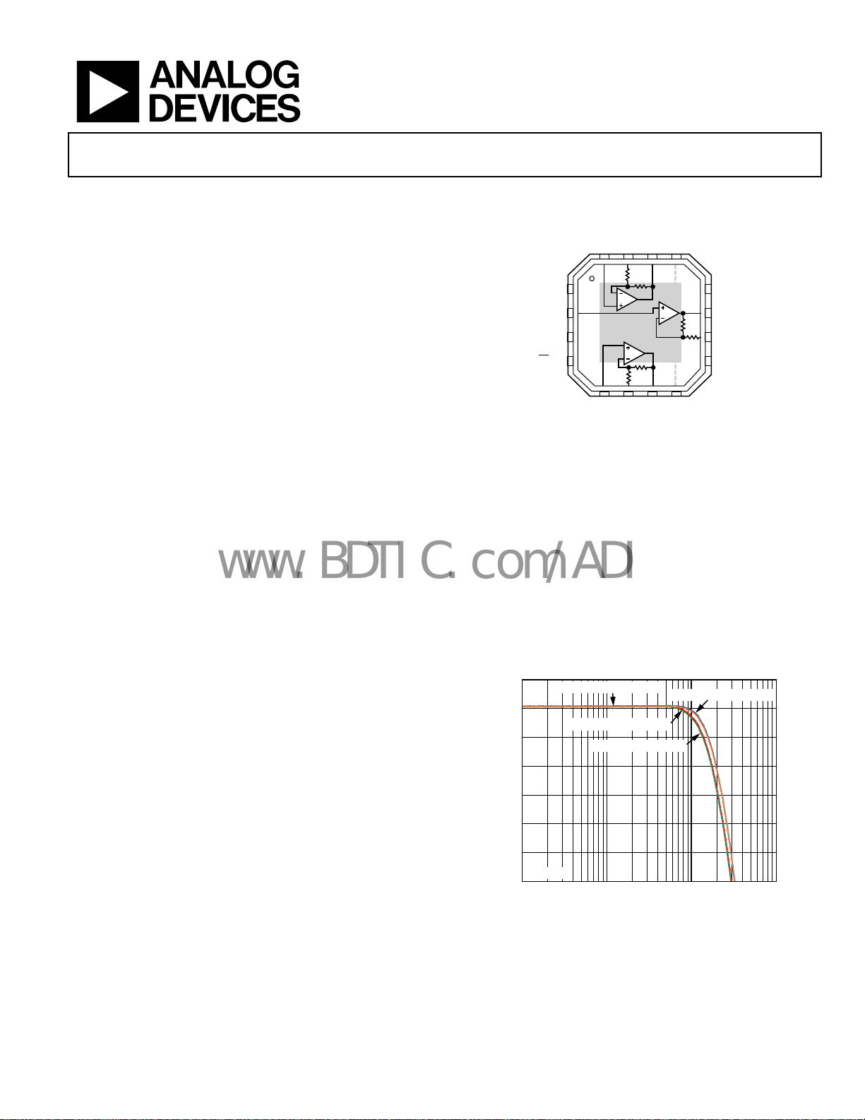
CONNECTION DIAGRAM
OUT1
OUT3
V
= 2V p-p
S
–V
S
–V
= 3.3V, V
S
12
+V
11 OUT2
10 –IN2
+V
9
.
S
= 1.4V p-p
OUT
S
S
07686-001
07686-058
–IN1
+IN1
16 15 14 13
1
NC
2+IN2
NC
PD
ADA4856-3
3
4
5678
–IN3
+IN3
NOTES
1. NC = NO CONNECT .
2. EXPOSED PAD CONNECTED TO –V
Figure 1.
7
6
5
4
3
2
CLOSED-LOOP GAIN (dB)
1
0
1 10 100 1000
VS= 5V, V
VS= 3.3V, V
RL= 150
Figure 2. Large Signal Frequency Response
= 1.4V p-p
OUT
= 2V p-p
OUT
= 5V, V
V
S
OUT
FREQUENCY (MHz)
Rev. 0
Information furnished by Analog Devices is believed to be accurate and reliable. However, no
responsibility is assumed by Analog Devices for its use, nor for any infringements of patents or other
rights of third parties that may result from its use. Specifications subject to change without notice. No
license is granted by implication or otherwise under any patent or patent rights of Analog Devices.
Trademarks and registered trademarks are the property of their respective owners.
One Technology Way, P.O. Box 9106, Norwood, MA 02062-9106, U.S.A.
Tel: 781.329.4700 www.analog.com
Fax: 781.461.3113 ©2008 Analog Devices, Inc. All rights reserved.
Page 2

ADA4856-3
www.BDTIC.com/ADI
TABLE OF CONTENTS
Features .............................................................................................. 1
Applications ....................................................................................... 1
Connection Diagram ....................................................................... 1
General Description ......................................................................... 1
Revision History ............................................................................... 2
Specifications ..................................................................................... 3
5 V Operation ............................................................................... 3
3.3 V Operation ............................................................................ 4
Absolute Maximum Ratings ............................................................ 5
Thermal Resistance ...................................................................... 5
Maximum Power Dissipation ..................................................... 5
ESD Caution .................................................................................. 5
Pin Configuration and Function Descriptions ............................. 6
Typical Performance Characteristics ............................................. 7
Theory of Operation ...................................................................... 12
Applications Information .............................................................. 13
Using the ADA4856-3 in Gains Equal to +1, −1 ........................ 13
Using the ADA4856-3 in Gains Equal to +3, +4, and +5 ..... 14
20 MHz Active Low-Pass Filter ................................................ 15
Video Line Driver ....................................................................... 15
Single-Supply Operation ........................................................... 16
Power Down ................................................................................ 16
Layout Considerations ............................................................... 16
Power Supply Bypassing ............................................................ 16
Outline Dimensions ....................................................................... 17
Ordering Guide .......................................................................... 17
REVISION HISTORY
10/08—Revision 0: Initial Version
Rev. 0 | Page 2 of 20
Page 3
ADA4856-3
www.BDTIC.com/ADI
SPECIFICATIONS
5 V OPERATION
TA = 25°C, +VS = 5 V, −VS = 0 V, G = +2, RL = 150 Ω to midsupply, unless otherwise noted.
Table 1.
Parameter Test Conditions Min Typ Max Unit
DYNAMIC PERFORMANCE
−3 dB Bandwidth VO = 0.1 V p-p 370 MHz
V
V
Bandwidth for 0.1 dB Flatness VO = 1.4 V p-p 90 MHz
V
Slew Rate VO = 2 V step 800 V/μs
Settling Time to 0.1% (Rise/Fall) VO = 2 V step 4.8/5.2 ns
NOISE/DISTORTION PERFORMANCE
Harmonic Distortion (HD2/HD3) fC = 5 MHz, VO = 2 V p-p, RL = 1 kΩ −92/−110 dBc
f
Crosstalk, Output to Output f = 5 MHz, G = +2 −80 dBc
Input Voltage Noise f = 100 kHz 14 nV/√Hz
Input Current Noise f = 100 kHz 2 pA/√Hz
Differential Gain Error 0.01 %
Differential Phase Error 0.01 Degrees
DC PERFORMANCE
Input Offset Voltage 1.3 3.4 mV
Input Offset Voltage Drift 5.5 μV/°C
Input Bias Current −3.8 μA
Input Offset Current ±0.05 μA
Closed-Loop Gain 1.95 2 2.05 V/V
Open-Loop Gain 90 dB
INPUT CHARACTERISTICS
Input Resistance 3.2 MΩ
Input Capacitance 0.5 pF
Input Common-Mode Voltage Range −VS − 0.2 +VS − 1 V
Common-Mode Rejection Ratio VCM = −0.2 V to +4 V 94 dB
OUTPUT CHARACTERISTICS
Output Voltage Swing 0.1 to 4.9 V
Linear Output Current Per Amplifier HD2 ≤ −60 dBc, RL = 10 Ω 52 mA
POWER-DOWN
Turn-On Time 78 ns
Turn-Off Time 950 ns
Input Bias Current Enabled 0.2 μA
Powered down −125 μA
Turn-On Voltage 3.75 V
POWER SUPPLY
Operating Range 3 5.5 V
Quiescent Current per Amplifier 7.8 mA
Supply Current When Disabled 1.1 mA
Power Supply Rejection Ratio ∆VS = 4.5 V to 5.5 V 96 dB
= 1.4 V p-p 225 MHz
O
= 2 V p-p 200 MHz
O
= 2 V p-p 74 MHz
O
= 20 MHz, VO = 2 V p-p, RL = 1 kΩ −68/−71 dBc
C
Rev. 0 | Page 3 of 20
Page 4
ADA4856-3
www.BDTIC.com/ADI
3.3 V OPERATION
TA = 25°C, +VS = 3.3 V, −VS = 0 V, G = +2, RL = 150 Ω to midsupply, unless otherwise noted.
Table 2.
Parameter Test Conditions Min Typ Max Unit
DYNAMIC PERFORMANCE
−3 dB Bandwidth VO = 0.1 V p-p 370 MHz
V
Bandwidth for 0.1 dB Flatness VO = 2 V p-p 77 MHz
Slew Rate VO = 2 V step 800 V/μs
Settling Time to 0.1% (Rise/Fall) VO = 2 V step 4.8/7 ns
NOISE/DISTORTION PERFORMANCE
Harmonic Distortion (HD2/HD3) fC = 5 MHz, VO = 2 V p-p, RL = 1 kΩ −95/−128 dBc
f
Crosstalk, Output to Output f = 5 MHz, G = +2 −78 dBc
Input Voltage Noise f = 100 kHz 14 nV/√Hz
Input Current Noise f = 100 kHz 2 pA/√Hz
Differential Gain Error 0.01 %
Differential Phase Error 0.01 Degrees
DC PERFORMANCE
Input Offset Voltage 1.2 3 mV
Input Offset Voltage Drift 5.5 μV/°C
Input Bias Current −3.8 μA
Input Offset Current ±0.05 μA
Closed-Loop Gain 1.95 2 2.05 V/V
Open-Loop Gain 90 dB
INPUT CHARACTERISTICS
Input Resistance 3.2 MΩ
Input Capacitance 0.5 pF
Input Common-Mode Voltage Range −VS − 0.2 +VS − 1 V
Common-Mode Rejection Ratio VCM = −0.2 V to +2.3 V 94 dB
OUTPUT CHARACTERISTICS
Output Voltage Swing, Load Resistance 0.1 to 3.22 V
Linear Output Current Per Amplifier HD2 ≤ −60 dBc, RL = 10 Ω 49 mA
POWER-DOWN
Turn-On Time 78 ns
Turn-Off Time 950 ns
Turn-On Voltage 2.05 V
POWER SUPPLY
Operating Range 3 5.5 V
Quiescent Current per Amplifier 7.5 mA
Quiescent Current When Powered Down 0.98 mA
Power Supply Rejection Ratio ∆VS = 2.97 V to 3.63 V 94 dB
= 2 V p-p 225 MHz
O
= 20 MHz, VO = 2 V p-p, RL = 1 kΩ −74/−101 dBc
C
Rev. 0 | Page 4 of 20
Page 5
ADA4856-3
www.BDTIC.com/ADI
ABSOLUTE MAXIMUM RATINGS
Table 3.
Parameter Rating
Supply Voltage 6 V
Internal Power Dissipation1 See Figure 3
Common-Mode Input Voltage (−VS − 0.2 V) to (+VS − 1 V)
Differential Input Voltage ±VS
Output Short-Circuit Duration Observe power curves
Storage Temperature Range −65°C to +125°C
Operating Temperature Range −40°C to +105°C
Lead Temperature (Soldering, 10 sec) 300°C
1
Specification is for device in free air.
Stresses above those listed under Absolute Maximum Ratings
may cause permanent damage to the device. This is a stress
rating only; functional operation of the device at these or any
other conditions above those indicated in the operational
section of this specification is not implied. Exposure to absolute
maximum rating conditions for extended periods may affect
device reliability.
THERMAL RESISTANCE
θJA is specified for the worst-case conditions, that is, θJA is specified
for a device soldered in a circuit board for surface-mount packages.
Table 4.
Package Type θJA θ
16-Lead LFCSP 67 17.5 °C/W
Unit
JC
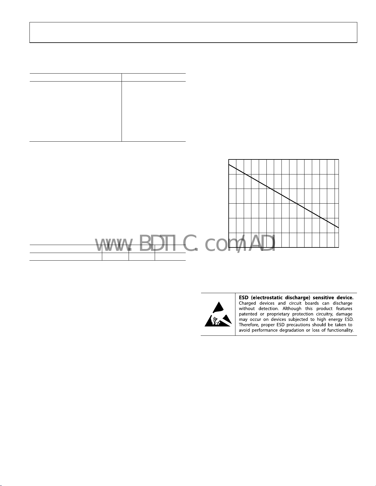
MAXIMUM POWER DISSIPATION
The maximum power that can be safely dissipated by the
ADA4856-3 is limited by the associated rise in junction
temperature. The maximum safe junction temperature for
plastic encapsulated devices is determined by the glass transition
temperature of the plastic, approximately 150°C. Temporarily
exceeding this limit may cause a shift in parametric performance
due to a change in the stresses exerted on the die by the package.
Exceeding a junction temperature of 175°C for an extended
period can result in device failure.
To ensure proper operation, it is necessary to observe the
maximum power derating curves.
3.0
2.5
2.0
1.5
1.0
0.5
MAXIMUM POWER DISSIPATION (W)
0
–40
–30
Figure 3. Maximum Power Dissipation vs. Ambient Temperature
0
–20
102030405060708090
–10
AMBIENT TEMPERATURE (°C)
07686-103
100
ESD CAUTION
Rev. 0 | Page 5 of 20
Page 6
ADA4856-3
www.BDTIC.com/ADI
PIN CONFIGURATION AND FUNCTION DESCRIPTIONS
–IN1
+IN1
16 15 14 13
S
–V
OUT1
NC
1
2+IN2
3
NC
4
PD
NOTES
1. NC = NO CONNECT .
2. EXPOSED PAD CONNECTED TO –V
ADA4856-3
TOP VIEW
(Not to Scale)
5678
–IN3
+IN3
OUT3
12
11 OUT2
10 –IN2
9
S
–V
S
Figure 4. Pin Configuration
Table 5. Pin Function Descriptions
Pin No. Mnemonic Description
1 NC No Connect.
2 +IN2 Noninverting Input 2.
3 NC No Connect.
4
PD
Power Down.
5 +IN3 Noninverting Input 3.
6 −IN3 Inverting Input 3.
7 OUT3 Output 3.
8 −VS Negative Supply.
9 +VS Positive Supply.
10 −IN2 Inverting Input 2.
11 OUT2 Output 2.
12 +VS Positive Supply.
13 −VS Negative Supply.
14 OUT1 Output 1.
15 −IN1 Inverting Input 1.
16 +IN1 Noninverting Input 1.
17 (EPAD) Exposed Pad (EPAD) The exposed pad must be connected to −VS.
+V
S
+V
S
.
07686-003
Rev. 0 | Page 6 of 20
Page 7

ADA4856-3
www.BDTIC.com/ADI
TYPICAL PERFORMANCE CHARACTERISTICS
TA = 25°C, +VS = 5 V, G = +2, RL = 150 Ω, large signal V
7
6
5
4
VS= 5V
V
= 3.3V
S
= 2 V p-p, small signal V
OUT
= 100 mV p-p, unless otherwise noted.
OUT
7
6
5
4
VS= 5V, V
VS= 3.3V, V
V
OUT
= 5V, V
S
= 1.4V p-p
= 2V p-p
OUT
OUT
V
= 2V p-p
S
= 3.3V, V
OUT
= 1.4V p-p
3
2
CLOSED-LOOP GAIN (dB)
1
0
1 10 100 1000
FREQUENCY (MHz)
Figure 5. Small Signal Frequency Response vs. Supply Voltage
6.2
6.1
6.0
VS= 3.3V, V
VS= 5V, V
CLOSED-LOOP GAIN (dB)
5.9
5.8
1 10 100 1000
= 3.3V, V
V
S
OUT
= 2V p-p
OUT
= 2V p-p
OUT
FREQUENCY (MHz)
= 1.4V p-p
VS= 5V, V
OUT
= 1.4V p-p
Figure 6. Large Signal 0.1 dB Flatness vs. Supply Voltage
7
= 1k
6
5
4
3
RL= 150
R
L
3
2
CLOSED-LOOP GAIN (dB)
1
07686-005
0
1 10 100 1000
FREQUENCY (MHz)
07686-008
Figure 8. Large Signal Frequency Response vs. Supply Voltage
2
T
= +105°C
A
0
TA = +25°C
–2
–4
CLOSED-LOOP GAIN (dB)
–6
07686-006
–8
1M 10M 100M 1G
TA= +85°C
TA= +105°C
TA= –40°C
FREQUENCY (Hz)
= –40°C
T
A
TA = +25°C
= +85°C
T
A
07686-009
Figure 9. Small Signal Frequency Response vs. Temperature
6
4
2
0
CL = 4.4pF
C
L
CL =6.6pF
=2.2pF
2
CLOSED-LOOP GAIN (dB)
1
0
1 10 100 1000
FREQUENCY (MHz)
07686-007
Figure 7. Small Signal Frequency Response vs. Load Resistance
Rev. 0 | Page 7 of 20
–2
CLOSED-LOOP GAIN (dB)
–4
–6
1 10 100 1000
FREQUENCY (MHz)
Figure 10. Small Signal Frequency Response vs. Capacitive Load
07686-010
Page 8

ADA4856-3
–
–
–
www.BDTIC.com/ADI
50
RL= 1k
–60
V
= 2V p-p
OUT
HD3
HD2
0.1110
FREQUENCY (MHz)
DISTORTION (dBc)
–70
–80
–90
–100
–110
–120
–130
–140
Figure 11. Harmonic Distortion vs. Frequency
0
–20
–40
–60
–80
FORWARD ISOLATIO N (dB)
–100
–120
0.1 1 10 100 1000
OUT3
OUT2
FREQUENCY (MHz)
OUT1
Figure 12. Forward Isolation vs. Frequency
0
–10
–20
–30
–40
–50
PSRR (dB)
–60
–70
–80
–90
–100
0.01 1001010.1
FREQUENCY (MHz)
+PSRR
–PSRR
Figure 13. Power Supply Rejection Ratio (PSRR) vs. Frequency
100
07686-011
07686-012
07686-013
50
RL= 1k
–60
V
= 1V p-p
OUT
V
= 3.3V
S
HD2
0.1 1
FREQUENCY (MHz)
DISTORTION (dBc)
–70
–80
–90
–100
–110
–120
–130
–140
Figure 14. Harmonic Distortion vs. Frequency
10
–20
–30
–40
–50
–60
–70
–80
–90
ALL HOSTILE CROSST ALK (dB)
–100
–110
–120
1M 10M 100M
IN1, IN3, OUT2
FREQUENCY (Hz)
Figure 15. Crosstalk vs. Frequency
0.5
0.4
0.3
0.2
0.1
0
–0.1
SETTLING TIME (%)
–0.2
–0.3
–0.4
–0.5
TIME (2ns/DIV)
Figure 16. Settling Time
HD3
10 100
IN1, IN2, OUT3
IN2, IN3, OUT1
07686-014
07686-015
07685-024
Rev. 0 | Page 8 of 20
Page 9

ADA4856-3
www.BDTIC.com/ADI
1k
25.0
VS= 5V
100
VOLTAGE NOISE (nV/Hz)
10
100 1k 10k 100k 1M
FREQUENCY (Hz)
Figure 17. Output Voltage Noise vs. Frequency
0.06
0.04
0.02
0
–0.02
OUTPUT VOLTAGE (V)
= 5V
V
S
VS = 3.3V
24.5
24.0
23.5
23.0
QUIESCENT CURRENT (mA)
22.5
07686-017
22.0
2.7 3.0 3.3 3.6 3.9 4.2 4.5 4.8 5.1 5.4
SUPPLY VOLTAGE (V)
07686-057
Figure 20. Quiescent Current vs. Supply Voltage
1.5
= 5V
V
S
1.0
0.5
0
–0.5
OUTPUT VOLTAGE (V)
VS = 3.3V
–0.04
–0.06
TIME (10n s/DIV)
Figure 18. Small Signal Transient Response vs. Supply Voltage
0.08
0.06
OUTPUT VOLTAGE (V)
0.04
0.02
0
–0.02
–0.04
–0.06
–0.08
TIME (10n s/DIV)
CL = 2.2pF
C
= 4.4pF
L
C
= 6.6pF
L
Figure 19. Small Signal Transient Response vs. Capacitive Load
–1.0
07686-018
–1.5
TIME (10n s/DIV)
07686-021
Figure 21. Large Signal Transient Response vs. Supply Voltage
1.5
1.0
0.5
0
–0.5
OUTPUT VO LTAGE (V )
–1.0
07686-019
–1.5
TIME (10n s/DIV)
CL = 2.2pF
C
= 4.4pF
L
C
= 6.6pF
L
07686-022
Figure 22. Large Signal Transient Response vs. Capacitive Load
Rev. 0 | Page 9 of 20
Page 10

ADA4856-3
www.BDTIC.com/ADI
0.08
1.5
0.06
OUTPUT VOLTAGE (V)
0.04
0.02
0
–0.02
–0.04
–0.06
VS= 3.3V
–0.08
TIME (10n s/DIV)
CL = 2.2pF
C
= 4.4pF
L
C
= 6.6pF
L
Figure 23. Small Signal Transient Response vs. Capacitive Load
4
2 × V
3
2
1
0
VOLTAGE (V)
–1
–2
–3
–4
V
OUT
IN
TIME (50n s/DIV)
Figure 24. Output Overdrive Recovery
3.0
2.5
2.0
1.5
1.0
0.5
VOLTAGE (V)
0
–0.5
–1.0
–1.5
V
PD
TIME (1us/DIV)
V
OUT
Figure 25. Turn-On/Turn-Off Time
1.0
0.5
0
–0.5
OUTPUT VOLTAGE (V)
–1.0
07686-023
VS= 3.3V
–1.5
TIME (10n s/DIV)
CL = 2.2pF
C
= 4.4pF
L
C
= 6.6pF
L
07686-026
Figure 26. Large Signal Transient Response vs. Capacitive Load
2.5
2 × V
2.0
1.5
1.0
0.5
0
–0.5
VOLTAGE (V)
–1.0
–1.5
–2.0
07686-025
–2.5
V
OUT
VS= 3.3V
IN
TIME (50n s/DIV)
07686-028
Figure 27. Output Overdrive Recovery
23.6
23.4
23.2
23.0
22.8
22.6
22.4
QUIESCENT CURRENT (mA)
22.2
22.0
07686-056
21.8
–40 –25 –10 5 20
VS = 5V
VS = 3.3V
35 65 80 110 12550 95
TEMPERATURE (°C)
07686-132
Figure 28. Quiescent Current vs. Temperature
Rev. 0 | Page 10 of 20
Page 11

ADA4856-3
www.BDTIC.com/ADI
1.8
1.7
1.6
1.5
1.4
1.3
1.2
1.1
OFFSET VOLTAGE (mV)
1.0
0.9
0.8
–40 –20 0 20 40 60 80 100 120
TEMPERATURE (°C)
Figure 29. Offset Drift vs. Temperature
100
10
07686-034
5.00
4.95
4.90
4.85
4.80
4.75
4.70
SATURATION VOLTAGE (mV)
4.65
4.60
0.01 0.1 1 10 100
LOAD CURRENT (mA)
07686-038
Figure 31. Output Saturation Voltage vs. Load Current
1
OUTPUT IM PEDENCE ()
0.1
0.01
100k 1M 10M 100M 1G
FREQUENCY (Hz)
07686-135
Figure 30. Output Impedance vs. Frequency
Rev. 0 | Page 11 of 20
Page 12

ADA4856-3
V
www.BDTIC.com/ADI
THEORY OF OPERATION
The ADA4856-3 is a voltage feedback op amp that employs a
new input stage that achieves a high slew rate while maintaining
a wide common-mode input range. The input common-mode
range of the ADA4856-3 extends from 200 mV below the negative
rail to about 1 V from the positive rail. This feature makes the
ADA4856-3 ideal for low voltage single-supply applications. In
addition, this new input stage does not sacrifice noise performance
for slew rate. At 14 nV/√Hz, the ADA4856-3 is one of the
lowest noise rail-to-rail output video amplifiers in the market.
Besides a novel input stage, the ADA4856-3 employs the Analog
Devices, Inc., patented rail-to-rail output stage. This output
stage makes an efficient use of the power supplies, allowing the
op amp to drive up to three video loads to within 300 mV from
both rails. In addition, this output stage provides the amplifier
with very fast overdrive characteristics, an important property
in video applications.
The ADA4856-3 comes in a 16-lead LFCSP that has an exposed
thermal pad for lower operating temperature. This pad is connected
internally to the negative rail. To avoid printed circuit board (PCB)
layout problems, the ADA4856-3 features a new pinout flow that
is optimized for video applications. As shown in Figure 4, the
feedback and gain resistors are on-chip, which minimizes the
number of components needed and improves the design layout.
The ADA4856-3 is fabricated in Analog Devices dielectrically
isolated eXtra Fast Complementary Bipolar 3 (XFCB3) process,
which results in the outstanding speed and dynamic range
displayed by the amplifier.
+
+IN
–IN
S
G
m1
–V
S
Figure 32. High Level Design Schematic
C
1
G
m2
R
C
OUT
07686-147
Rev. 0 | Page 12 of 20
Page 13

ADA4856-3
V
V
V
V
V
www.BDTIC.com/ADI
APPLICATIONS INFORMATION
USING THE ADA4856-3 IN GAINS EQUAL TO +1, −1
The ADA4856-3 was designed to offer outstanding video
performance, simplify applications, and minimize board area.
The ADA4856-3 is a triple amplifier with on-chip feedback
and gain set resistors. The gain is fixed internally at G = +2. The
inclusion of the on-chip resistors not only simplifies the design of
the application but also eliminates six surface-mount resistors,
saving valuable board space and lowering assembly costs.
Whereas the ADA4856-3 has a fixed gain of G = +2, it can be
used in other gain configurations, such as G = −1 and G = +1.
Unity-Gain Operation
Option 1
There are two options for obtaining unity gain (G = +1). The
first is shown in Figure 33. In this configuration, the –IN input
pin is tied to the output (feedback is now provided with the two
internal 402 Ω resistors in parallel), and the input is applied to
the noninverting input. The noise gain for this configuration is 1.
+
S
10µF
0.1µF
+
S
10µF
0.1µF
R
F
R
G
V
V
IN
R
T
0.1µF
10µF
–V
S
GAIN OF +1
OUT
07686-030
Figure 34. Unity Gain of Option 2
Inverting Unity-Gain Operation
In this configuration, the noninverting input is tied to ground
and the input signal is applied to the inverting input. The noise
gain for this configuration is +2, see Figure 35.
+
S
10µF
0.1µF
V
IN
R
T
0.1µF
10µF
–V
S
GAIN OF +1
OUT
07686-032
Figure 33. Unity Gain of Option 1
Option 2
Another option exists for running the ADA4856-3 as a unitygain amplifier. In this configuration, the noise gain is +2, see
Figure 34. The frequency response and transient response for
this configuration closely match the gain of +2 plots because the
noise gains are equal. This method does have twice the noise gain
of Option 1; however, in applications that do not require low noise,
Option 2 offers less peaking and ringing. By tying the inputs
together, the net gain of the amplifier becomes 1. Equation 1 shows
the transfer characteristic for the schematic shown in Figure 34.
OUT
⎜
⎝
⎛
−
⎜
VV
=
IN
which simplifies to V
F
R
G
OUT
⎟
V
+
⎟
⎠
= VIN.
⎜
IN
⎜
⎝
⎛
⎞
R
⎞
RR
+
F
G
⎟
(1)
⎟
R
G
⎠
IN
R
T
0.1µF
10µF
–V
S
GAIN OF –1
V
OUT
07686-031
Figure 35. Inverting Configuration (G = −1)
Figure 36 shows the small signal frequency response for both
gain of +1 (Option 1 and Option 2) and gain of −1 configurations.
It is clear that G = +1, Option 2 has better flatness and no peaking
compared to Option 1.
6
VS = 5V
R
= 100
L
V
= 100mV p-p
OUT
3
0
OPTION 2
–3
MAGNITUDE (dB)
–6
–9
G = +1
OPTION 1
G = +1
G = –1
Rev. 0 | Page 13 of 20
–12
1 10 100 1000
FREQUENCY (MHz )
Figure 36. G = +1 and G = −1
07686-044
Page 14

ADA4856-3
–
V
–
V
–
V
www.BDTIC.com/ADI
USING THE ADA4856-3 IN GAINS EQUAL TO +3, +4, AND +5
Depending on certain applications, it might be useful to have a
fixed gain amplifier that can provide various gains. The advantage
of having a fixed gain amplifier is the ease of layout, the reduced
number of components needed, and the matching of the gain
and feedback resistors.
Gain of +3 Configuration
Figure 37 shows the ADA4856-3 used as an amplifier with a
fixed gain of +3. No external resistors are required, just a simple
S
V
OUT
S
10µF
S
V
OUT
S
10µF
+
IN
+
to U1,
IN
10µF
07686-045
going in
.
OUT
10µF
07686-046
trace connecting certain inputs and outputs. Connect V
which is set to a gain of +2, and U2, which is set to unity. U3 then
takes the output of U1 and gains it up by +2 and subtracts the
output of U2 to produce V
. As shown in Figure 40, the large
OUT
signal frequency response for G = +3 is flat out to 65 MHz, with a
bandwidth of 165 MHz, a 2 V p-p output voltage, and a 100 Ω load.
S
16 15 14 13
PD
1
2
ADA4856-3
3
4
567
V
IN
0.1µF
0.1µF
12
+V
11
10
9
+V
8
–V
S
+
0.1µF
0.1µF
Figure 37. Gain of +3
Gain of +4 Configuration
To get a gain of +4, set one amplifier to a gain of +1 and set the
other two amplifiers to a gain of +2. Figure 38 shows V
U2 at unity, then U1 takes the output of U2 and gains it by +2, and
then feeds it to U3, which also gains it by +2 to produce V
S
16 15 14 13
1
2
ADA4856-3
3
4
PD
V
IN
567
Figure 38. Gain of +4
0.1µF
0.1µF
12
+V
11
10
9
+V
8
–V
S
+
0.1µF
0.1µF
As shown in Figure 40, the large signal frequency response
for G = +4 is also flat out to 65 MHz, and it has a bandwidth
of 180 MHz.
Gain of+ 5 Configuration
The gain of +5 is very similar to the G = +3 configuration but with
U2 set to a gain of −1, which ends up being added to twice the
output of U1 to generate V
PD
1
2
ADA4856-3
3
4
V
IN
with G = +5.
OUT
S
16 15 14 13
567
8
–V
S
Figure 39. Gain of +5
0.1µF
12
11
10
9
0.1µF
0.1µF
0.1µF
+V
+V
+
S
V
S
10µF
+
OUT
10µF
07686-047
Figure 40 shows the large signal frequency response of the three
closed-loop gain sets (+3, +4, and +5) with flatness that extends
to 65 MHz and a −3 dB bandwidth of 150 MHz.
15
12
9
6
3
0
–3
–6
–9
CLOSED-LOOP GAIN (dB)
–12
–15
–18
RL= 100
= 5V
V
S
= 2V p-p
V
OUT
1 10 100 1000
G = +3
FREQUENCY (MHz)
G = +4
Figure 40. Large Signal Frequency Response for All Three Gains
G = +5
07686-048
Rev. 0 | Page 14 of 20
Page 15

ADA4856-3
V
www.BDTIC.com/ADI
20 MHz ACTIVE LOW-PASS FILTER
The ADA4856-3 triple amplifier lends itself to higher order
active filters. Figure 41 shows a 20 MHz, 6-pole, Sallen-Key
low-pass filter.
–
93.1R2604
V
IN
R1
C1
33pF
R3
113R4732
OP AMP
+
C2
22pF
C3
33pF
R5
121R6475
C5
47pF
Figure 41. 20 MHz, 6-Pole Low-Pass Filter
The filter has a gain of approximately 18 dB, which is set by
three fixed gain of 2 stages, and a flat frequency response out to
14 MHz. This type of filter is commonly used at the output of a
video DAC as a reconstruction filter. The frequency response of
the filter is shown in Figure 42.
20
10
FOUR POLES
TWO POLES
0
–10
–20
–30
MAGNITUDE (dB)
–40
–50
–60
1 10 100 200
Figure 42. 20 MHz, Low-Pass Filter Frequency Response
SIX POLES
FREQUENCY (MHz )
U1
C4
15pF
OUT1
–
U2
OP AMP
+
C6
15pF
OUT2
–
U3
OP AMP
+
OUT3
V
OUT
07686-050
07686-049
VIDEO LINE DRIVER
The ADA4856-3 was designed to excel in video driver applications.
Figure 43 shows a typical schematic for a video driver operating
on bipolar supplies.
75
V
(R)
V
(R)
IN
75
16 15 14 13
1
(G)
V
IN
(B)
V
IN
75
75
PD
2
ADA4856-3
3
4
567
Figure 43. Video Driver Schematic
In applications that require multiple video loads be driven
simultaneously, the ADA4856-3 can deliver. Figure 44 shows
the ADA4856-3 configured with triple video loads. Figure 45
shows the triple video load performance.
10µF
+V
S
0.1µF
–
ADA4856-3
75
VS= 5V
V
OUT
+
= 1V p-p
0.1µF
10µF
–V
S
RL= 150
RL= 75
RL= 50
FREQUENCY (MHz )
75
CABLE
IN
Figure 44. Video Driver Schematic for Triple Video Loads
6.5
6.0
5.5
5.0
4.5
4.0
MAGNITUDE (dB)
3.5
3.0
2.5
1 10 100 200
Figure 45. Large Signal Frequency Response for Various Loads
–V
–V
75
8
S
S
0.1µF
OUT
10µF
+
0.1µF
(B)
75
75
75
0.1µF
0.1µF
+V
S
+V
S
0.1µF
75
CABLE
75
CABLE
75
CABLE
75
+
75
75
75
V
OUT
10µF
(G)
1
V
OUT
V
2
OUT
3
V
OUT
07686-053
0.1µF
12
11
10
9
0.1µF
V
OUT
07686-051
07686-052
Rev. 0 | Page 15 of 20
Page 16

ADA4856-3
V
V
www.BDTIC.com/ADI
SINGLE-SUPPLY OPERATION POWER DOWN
The ADA4856-3 can operate in single-supply applications.
Figure 46 shows the schematic for a single 5 V supply video
driver. Resistors R2 and R4 establish the midsupply reference.
Capacitor C2 is the bypass capacitor for the midsupply reference.
Capacitor C1 is the input coupling capacitor, and C6 is the output
coupling capacitor. Capacitor C5 prevents constant current from
being drawn through the internal gain set resistor. Resistor R3
sets the ac input impedance of the circuit.
For more information on single-supply operation of op amps,
see “Avoiding Op-Amp Instability Problems In Single-Supply
Applications”, Analog Dialogue, Volume 35, Number 2, MarchMay, 2001, at www.analog.com.
C2
1µF
+5
C3
2.2µF
The ADA4856-3 is equipped with a PD (power-down) pin for
all three amplifiers. This allows the user to reduce the quiescent
supply current when an amplifier is inactive. The power-down
threshold levels are derived from the voltage applied to the +V
S
pin. When used in single-supply applications, this is especially
useful with conventional logic levels. The amplifier is enabled
when the voltage applied to the
pin is greater than +VS − 1.25 V.
PD
In a 5 V single-supply application, the typical threshold voltage
is +3.75 V, and in a 3.3 V dual-supply application, the typical
threshold voltage is +2 V. The amplifier is also enabled when the
pin is left floating (not connected). However, the amplifier is
PD
powered down when the voltage on the
from +V
. If the PD pin is not used, it is best to connect it to the
S
pin is lower than 2.5 V
PD
positive supply
R4
R2
50k
50k
+5V
R3
1k
V
IN
C1
R1
22µF
50
C5
22µF
Figure 46. AC-Coupled, Single-Supply Video Driver Schematic
C4
0.01µF
–V
S
C6
220µF
R5
75
ADA4856-3
R6
75
V
OUT
07686-035
In addition, the ADA4856-3 can be configured in dc-coupled,
single-supply operation. The common-mode input voltage
can go about 200 mV below ground, which makes it a true singlesupply part. However, in video applications, the black level is set
at 0 V, which means that the output of the amplifier must go to
the ground level as well. This part has a rail-to-rail output stage;
it can go as close as 100 mV from either rail. Figure 47 shows
the schematic for adding 50 mV dc offset to the input signal so
that the output is not clipped while still properly terminating
the input with 75 Ω.
5
C1
10µF
5V
R1
3.74k
V
IN
R2
76.8
Figure 47. DC-Coupled Single Supply Video Driver Schematic
C2
0.1µF
U1
–V
S
R3
75
ADA4856-3
R4
75
V
OUT
07686-156
Table 6. Power-Down Voltage Control
Pin 5 V ±2.5 V 3.3 V
PD
Not Active >3.75 V >1.25 V >2.05 V
Active <2 V <0 V <1.3 V
LAYOUT CONSIDERATIONS
As is the case with all high speed applications, careful attention
to printed circuit board (PCB) layout details prevents associated
board parasitics from becoming problematic. Proper RF design
technique is mandatory. The PCB should have a ground plane
covering all unused portions of the component side of the
board to provide a low impedance return path. Removing the
ground plane on all layers from the area near the input and output
pins reduces stray capacitance. Locate termination resistors and
loads as close as possible to their respective inputs and outputs.
Keep input and output traces as far apart as possible to minimize
coupling (crosstalk) though the board. Adherence to microstrip
or stripline design techniques for long signal traces (greater than
about 1 inch) is recommended.
POWER SUPPLY BYPASSING
Careful attention must be paid to bypassing the power supply pins
of the ADA4856-3. Use high quality capacitors with low equivalent
series resistance (ESR), such as multilayer ceramic capacitors
(MLCCs), to minimize supply voltage ripple and power dissipation.
A large, usually tantalum, 10 μF to 47 μF capacitor located in
proximity to the ADA4856-3 is required to provide good
decoupling for lower frequency signals. In addition, locate 0.1 μF
MLCC decoupling capacitors as close to each of the power supply
pins as is physically possible, no more than 1/8 inch away. The
ground returns should terminate immediately into the ground
plane. Locating the bypass capacitor return close to the load
return minimizes ground loops and improves performance.
Rev. 0 | Page 16 of 20
Page 17

ADA4856-3
www.BDTIC.com/ADI
OUTLINE DIMENSIONS
PIN 1
INDICATOR
1.00
0.85
0.80
12° MAX
SEATING
PLANE
4.00
BSC SQ
TOP
VIEW
0.80 MAX
0.65 TYP
0.35
0.30
0.25
3.75
BSC SQ
0.20 REF
0.60 MAX
0.65 BSC
0.05 MAX
0.02 NOM
COPLANARITY
0.75
0.60
0.50
0.08
0.60 MAX
(BOTTO M VIEW )
16
13
12
9
8
5
1.95 BSC
FOR PROPER CONNECTION OF
THE EXPOSED PAD, REFER TO
THE PIN CONF IGURATIO N AND
FUNCTION DES CRIPTIONS
SECTION OF THIS DATA SHEET.
PIN 1
INDICATOR
1
4
5
2
.
2
0
1
.
2
9
.
1
5
0.25 MIN
Q
S
COMPLIANT TO JEDEC STANDARDS MO-220-VGGC
072808-A
Figure 48.16-Lead Lead Frame Chip Scale Package [LFCSP_VQ]
4 mm × 4 mm Body, Very Thin Quad
(CP-16-4)
Dimensions shown in millimeters
ORDERING GUIDE
Model Temperature Range Package Description Package Option Ordering Quantity
ADA4856-3YCPZ-R2
ADA4856-3YCPZ-R7
ADA4856-3YCPZ-RL
1
Z = RoHS Compliant Part.
1
1
–40°C to +105°C 16-Lead LFCSP_VQ CP-16-4 1,500
1
–40°C to +105°C 16-Lead LFCSP_VQ CP-16-4 5,000
–40°C to +105°C 16-Lead LFCSP_VQ CP-16-4 250
Rev. 0 | Page 17 of 20
Page 18

ADA4856-3
www.BDTIC.com/ADI
NOTES
Rev. 0 | Page 18 of 20
Page 19

ADA4856-3
www.BDTIC.com/ADI
NOTES
Rev. 0 | Page 19 of 20
Page 20

ADA4856-3
www.BDTIC.com/ADI
NOTES
©2008 Analog Devices, Inc. All rights reserved. Trademarks and
registered trademarks are the property of their respective owners.
D07686-0-10/08(0)
Rev. 0 | Page 20 of 20
 Loading...