

Page 1
www.BDTIC.com/ADI
Low Cost 6-Channel HD/SD Video Filter
FEATURES FEATURES
Sixth-order filters Sixth-order filters
Transparent input sync tip clamp Transparent input sync tip clamp
−1 dB bandwidth of 26 MHz typical for HD −1 dB bandwidth of 26 MHz typical for HD
HD rejection @ 75 MHz: 48 dB typical HD rejection @ 75 MHz: 48 dB typical
NTSC differential gain: 0.19% NTSC differential gain: 0.19%
NTSC differential phase: 0.76° NTSC differential phase: 0.76°
Rail-to-rail outputs Rail-to-rail outputs
Low quiescent current: 32 mA typical Low quiescent current: 32 mA typical
Disable feature Disable feature
Output dc offset Output dc offset
APPLICATIONS APPLICATIONS
Set-top boxes Set-top boxes
DVD players and recorders DVD players and recorders
HDTVs HDTVs
Projectors Projectors
Personal video recorders Personal video recorders
GENERAL DESCRIPTION GENERAL DESCRIPTION
The ADA4420-6 is a low cost video reconstruction filter specifically
The ADA4420-6 is a low cost video reconstruction filter specifically
designed for consumer applications. It consists of six independent
designed for consumer applications. It consists of six independent
sixth-order Butterworth filters/buffers, three for standard
sixth-order Butterworth filters/buffers, three for standard
definition (Y/C or CVBS) and three for high definition
definition (Y/C or CVBS) and three for high definition
component signals (YPbPr or RGB).
component signals (YPbPr or RGB).
The ADA4420-6 operates from a single 5 V supply and has a
The ADA4420-6 operates from a single 5 V supply and has a
low quiescent current of 32 mA, making it ideal for applications
low quiescent current of 32 mA, making it ideal for applications
where power consumption is critical. A disable feature allows
where power consumption is critical. A disable feature allows
for further power conservation by reducing the supply current
for further power conservation by reducing the supply current
to less than 8 µA typical when the device is not in use.
to less than 8 µA typical when the device is not in use.
ADA4420-6
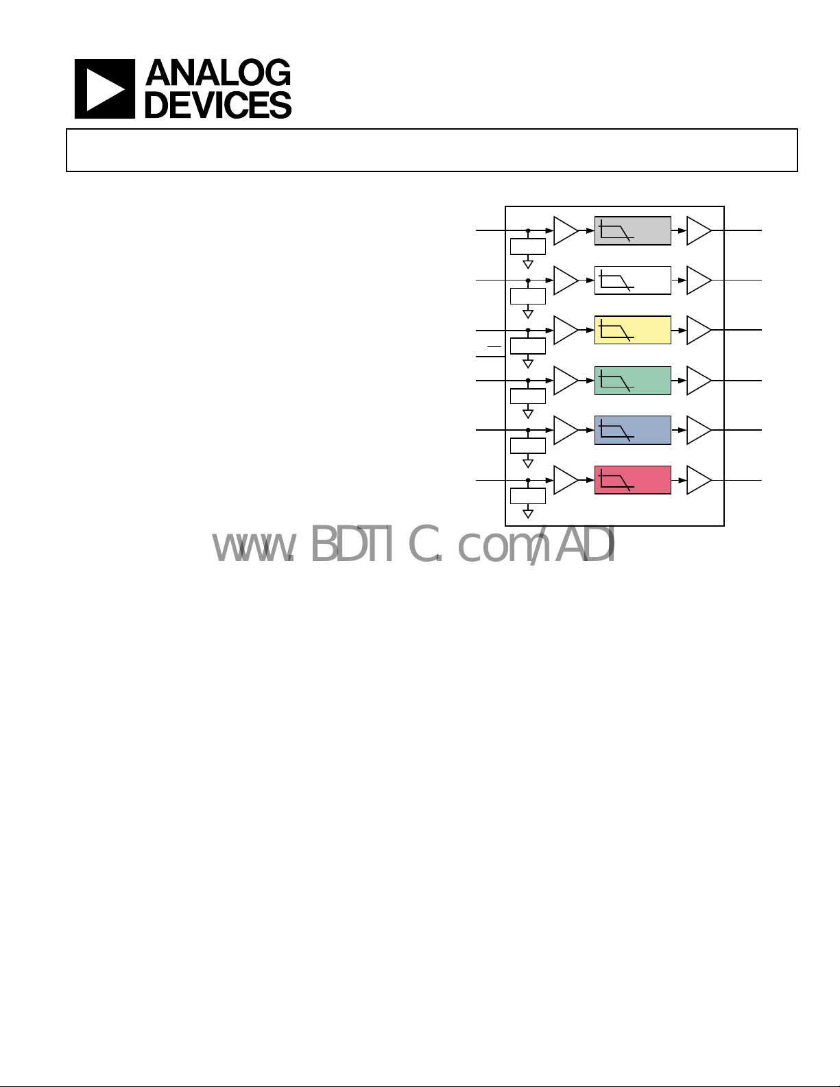
FUNCTIONAL BLOCK DIAGRAM FUNCTIONAL BLOCK DIAGRAM
INSD1
INSD2
INSD3
DIS
INHD1
INHD2
INHD3
CLAMP
CLAMP
CLAMP
CLAMP
CLAMP
CLAMP
×1
×1
×1
×1
×1
×1
Figure 1.
SD
SD
SD
HD
HD
HD
ADA4420-6
Each channel features a transparent sync tip clamp, allowing ac
coupling of the inputs without requiring dc restoration.
The output drivers on the ADA4420-6 have rail-to-rail output
capabilities with 6 dB gain. A built-in offset of 250 mV allows
the outputs to be dc-coupled, eliminating the need for large
coupling capacitors. Each output is capable of driving two 75 Ω
doubly terminated cables.
The ADA4420-6 is available in a 16-lead QSOP and operates in
the extended industrial temperature range of −40°C to +85°C.
OUTSD1
×2
OUTSD2
×2
OUTSD3
×2
OUTHD1
×2
OUTHD2
×2
OUTHD3
×2
07532-001
Rev. 0
Information furnished by Analog Devices is believed to be accurate and reliable. However, no
responsibility is assumed by Analog Devices for its use, nor for any infringements of patents or other
rights of third parties that may result from its use. Specifications subject to change without notice. No
license is granted by implication or otherwise under any patent or patent rights of Analog Devices.
Trademarks and registered trademarks are the property of their respective owners.
One Technology Way, P.O. Box 9106, Norwood, MA 02062-9106, U.S.A.
Tel: 781.329.4700 www.analog.com
Fax: 781.461.3113 ©2008 Analog Devices, Inc. All rights reserved.
Page 2

ADA4420-6
www.BDTIC.com/ADI
TABLE OF CONTENTS
Features .............................................................................................. 1
Applications ....................................................................................... 1
General Description ......................................................................... 1
Functional Block Diagram .............................................................. 1
Revision History ............................................................................... 2
Specifications ..................................................................................... 3
Absolute Maximum Ratings ............................................................ 4
Thermal Resistance ...................................................................... 4
Maximum Power Dissipation ..................................................... 4
ESD Caution .................................................................................. 4
Pin Configuration and Function Descriptions ............................. 5
REVISION HISTORY
8/08—Revision 0: Initial Version
Typical Performance Characteristics ..............................................6
Test Circuits ........................................................................................9
Applications Information .............................................................. 10
Overview ..................................................................................... 10
Disable ......................................................................................... 10
Input and Output Coupling ...................................................... 10
Printed Circuit Board (PCB) Layout ....................................... 10
Video Encoder Reconstruction Filter ...................................... 10
Outline Dimensions ....................................................................... 12
Ordering Guide .......................................................................... 12
Rev. 0 | Page 2 of 12
Page 3
ADA4420-6
www.BDTIC.com/ADI
SPECIFICATIONS
VS = 5 V, TA = 25°C, VO = 2.0 V p-p, RL = 150 Ω, dc-coupled inputs, ac-coupled outputs, unless otherwise noted. See Figure 17, Figure 18,
and Figure 19 for the test circuits.
Table 1.
Parameter Test Conditions/Comments Min Typ Max Unit
OVERALL PERFORMANCE
DC Voltage Gain All channels 5.8 6.0 6.2 dB
Input Voltage Range, All Inputs 0 to 2.1 V
Output Voltage Range, All Outputs 0.25 to 4.6 V
Linear Output Current per Channel 30 mA
Filter Input Bias Current 1 μA
SD CHANNEL DYNAMIC PERFORMANCE
−1 dB Bandwidth 8.6 MHz
−3 dB Bandwidth 8.5 10 MHz
Out-of-Band Rejection f = 27 MHz 42 45 dB
Crosstalk f = 1 MHz −68 dB
Total Harmonic Distortion f = 1 MHz, VO = 1.4 V p-p, dc-coupled outputs 0.02 %
Signal-to-Noise Ratio f = 100 kHz to 6 MHz, unweighted 70 dB
Propagation Delay 57 ns
Group Delay Variation f = 100 kHz to 5 MHz 16 ns
Differential Gain
Differential Phase
HD CHANNEL DYNAMIC PERFORMANCE
−1 dB Bandwidth 26 MHz
−3 dB Bandwidth 27 31 MHz
Out-of-Band Rejection f = 75 MHz 43 48 dB
Crosstalk f = 1 MHz −68 dB
Total Harmonic Distortion f = 10 MHz, VO = 1.4 V p-p, dc-coupled outputs 0.57 %
Signal-to-Noise Ratio f = 100 kHz to 30 MHz, unweighted 66 dB
Propagation Delay 15 ns
Group Delay Variation f = 100 kHz to 30 MHz 11 ns
DC CHARACTERISTICS
Operating Voltage 4.75 to 5.25 V
Quiescent Supply Current
PSRR HD channel, referred to output 35 41 dB
SD channel, referred to output 40 45 dB
Output DC Offset All channels 135 250 375 mV
DISABLE Assert Voltage 1.9 V
DISABLE Assert Time 20 ns
DISABLE De-Assert Time 450 ns
DISABLE Input Bias Current
Input-to-Output Isolation
NTSC; ac-coupled inputs, dc-coupled outputs;
see Figure 18
NTSC; ac-coupled inputs, dc-coupled outputs;
see Figure 18
Active, DIS
Disabled, DIS
Disabled, DIS
Disabled, DIS
= 1
= 0
= 0
= 0, f = 5 MHz
0.19 %
0.76 Degrees
32 36 mA
7 13 μA
−6.8 μA
−96 dB
Rev. 0 | Page 3 of 12
Page 4
ADA4420-6
www.BDTIC.com/ADI
ABSOLUTE MAXIMUM RATINGS
Table 2.
Parameter Rating
Supply Voltage 5.5 V
Power Dissipation See Figure 2
Storage Temperature Range −65°C to +125°C
Operating Temperature Range −40°C to +85°C
Lead Temperature (Soldering, 10 sec) 300°C
Junction Temperature 150°C
Stresses above those listed under Absolute Maximum Ratings
may cause permanent damage to the device. This is a stress
rating only; functional operation of the device at these or any
other conditions above those indicated in the operational
section of this specification is not implied. Exposure to absolute
maximum rating conditions for extended periods may affect
device reliability.
THERMAL RESISTANCE
θJA is specified for the device soldered to a high thermal
conductivity 4-layer (2s2p) circuit board, as described in
EIA/JESD 51-7.
Table 3.
Package Type θJA θJC Unit
16-Lead QSOP 105 23 °C/W
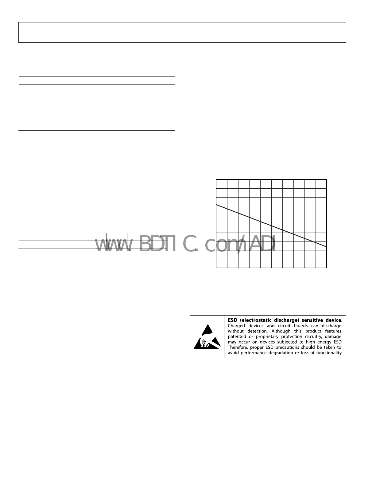
MAXIMUM POWER DISSIPATION
The maximum safe power dissipation in the ADA4420-6
package is limited by the associated rise in junction temperature
(T
) on the die. At approximately 150°C, which is the glass
J
transition temperature, the plastic changes its properties. Even
temporarily exceeding this temperature limit can change the
stresses that the package exerts on the die, permanently shifting
the parametric performance of the ADA4420-6. Exceeding a
junction temperature of 150°C for an extended time can result
in changes in the silicon devices, potentially causing failure.
The power dissipated in the package (P
) is the sum of the
D
quiescent power dissipation and the power dissipated in the
package due to the load drive for all outputs. The quiescent
power is the voltage between the supply pins (V
quiescent current (I
). The power dissipated due to load drive
S
) times the
S
depends on the particular application. For each output, the
power due to load drive is calculated by multiplying the load
current by the associated voltage drop across the device. The
power dissipated due to the loads is equal to the sum of the
power dissipations due to each individual load. RMS voltages
and currents must be used in these calculations.
Airflow increases heat dissipation, effectively reducing θ
.
JA
Figure 2 shows the maximum power dissipation in the package
vs. the ambient temperature for the 16-lead QSOP (105°C/W)
on a JEDEC standard 4-layer board. θ
2.0
1.8
1.6
1.4
1.2
1.0
0.8
0.6
0.4
MAXIMUM POWER DISSIPATION (W )
0.2
0
0 102030405060708090100
AMBIENT TEMPERATURE (°C)
Figure 2. Maximum Power Dissipation vs.
Ambient Temperature for a 4-Layer Board
values are approximate.
JA
07532-016
ESD CAUTION
Rev. 0 | Page 4 of 12
Page 5

ADA4420-6
3
www.BDTIC.com/ADI
PIN CONFIGURATION AND FUNCTION DESCRIPTIONS
INSD1
INSD2
INSD3
VCC
DIS
INHD1
INHD2
INHD
1
2
3
ADA4420-6
4
TOP VIEW
5
(Not to Scale)
6
7
8
Figure 3. Pin Configuration
16
15
14
13
12
11
10
9
OUTSD1
OUTSD2
OUTSD3
GND
GND
OUTHD1
OUTHD2
OUTHD3
Table 4. Pin Function Descriptions
Pin No. Mnemonic Description
1 INSD1 Standard Definition Input 1
2 INSD2 Standard Definition Input 2
3 INSD3 Standard Definition Input 3
4 VCC Power Supply
5
DIS
Disable/Power-Down Input
6 INHD1 High Definition Input 1
7 INHD2 High Definition Input 2
8 INHD3 High Definition Input 3
9 OUTHD3 High Definition Output 3
10 OUTHD2 High Definition Output 2
11 OUTHD1 High Definition Output 1
12 GND Ground
13 GND Ground
14 OUTSD3 Standard Definition Output 3
15 OUTSD2 Standard Definition Output 2
16 OUTSD1 Standard Definition Output 1
07532-002
Rev. 0 | Page 5 of 12
Page 6

ADA4420-6
www.BDTIC.com/ADI
TYPICAL PERFORMANCE CHARACTERISTICS
VS = 5.0 V, TA = 25°C, VO = 2.0 V p-p, RL = 150 Ω, dc-coupled inputs, ac-coupled outputs, unless otherwise noted. See Figure 17, Figure 18,
and Figure 19 for the test circuits.
10
0
–10
–20
–30
–40
GAIN (dB)
–50
–60
–70
–80
1 10 100
SD CHANNELS,
R
= 150Ω
L
FREQUENCY (MHz )
HD CHANNELS,
R
= 75Ω
L
HD CHANNELS,
R
= 150Ω
L
SD CHANNELS,
R
= 75Ω
L
Figure 4. Frequency Response vs. Load (RL)
10
0
–10
–20
–30
–40
GAIN (dB)
–50
HD –40°C
HD +25°C
–60
HD +85°C
SD –40°C
–70
SD +25°C
SD +85°C
–80
11010
FREQUENCY (MHz )
0
Figure 5. Frequency Response vs. Temperature
10
0
–10
–20
–30
–40
GAIN (dB)
–50
–60
SD VO = 100mV p-p
= 2.0V p-p
SD V
–70
–80
O
= 100mV p-p
HD V
O
= 2.0V p-p
HD V
O
11010
FREQUENCY (MHz )
0
Figure 6. Frequency Response vs. Amplitude
07532-004
07532-005
07532-006
1.0
SD CHANNELS,
R
= 75Ω
0.5
–0.5
–1.0
–1.5
NORMALIZE D GAIN (dB)
–2.0
–2.5
–3.0
L
0
SD CHANNELS,
R
= 150Ω
L
1 10 100
FREQUENCY (MHz )
Figure 7. Flatness vs. Load (R
HD CHANNELS,
R
= 75Ω
L
HD CHANNELS,
R
= 150Ω
L
)
L
07532-007
1.0
0.5
0
–0.5
–1.0
–1.5
NORMALIZED GAIN (dB)
HD –40°C
–2.0
HD +25°C
HD +85°C
SD –40°C
–2.5
SD +25°C
SD +85°C
–3.0
1 10 100
FREQUENCY (MHz )
07532-008
Figure 8. Flatness vs. Temperature
10
0
–10
–20
–30
–40
GAIN (dB)
–50
–60
–70
–80
110100
HD AC-COUPLED
FREQUENCY (MHz )
HD DC-COUPLED
SD AC-COUPLED
SD DC-COUPLED
Figure 9. Frequency Response vs. Output Coupling
07532-017
Rev. 0 | Page 6 of 12
Page 7

ADA4420-6
www.BDTIC.com/ADI
100
90
80
70
60
50
40
GROUP DELAY (ns)
30
20
10
0
0.1 1 10 100
SD CHANNELS
HD CHANNELS
FREQUENCY (MHz )
Figure 10. Group Delay vs. Frequency
10k
DIS = 0
1k
07532-009
6
5
4
3
2
1
DISABLE VOLTAGE (V)
0
–1
–600 –400 –200 0 200 400 600 800 1000 1200
TIME (ns)
SD CHANNELS
HD CHANNELS
Figure 12. Enable Turn-On Time
36
35
34
33
32
07532-012
100
OUTPUT IM PEDANCE (Ω)
10
0.1 1 10 100
FREQUENCY (MHz)
Figure 11. Output Impedance vs. Frequency
31
SUPPLY CURRENT (mA)
30
29
28
–60 –40 –20 0 20 40 60 80 100
7532-011
TEMPERATURE ( °C)
7532-013
Figure 13. Supply Current vs. Temperature
Rev. 0 | Page 7 of 12
Page 8

ADA4420-6
www.BDTIC.com/ADI
0
–10
–20
–30
–40
–50
–60
CROSSTALK (dB)
SD CHANNELS
–70
–80
–90
0.1 1 10 100 1000
HD CHANNELS
FREQUENCY (MHz)
Figure 14. Crosstalk vs. Frequency
6
5
4
3
SD CHANNELS
07532-014
4.70
4.68
4.66
4.64
4.62
4.60
4.58
4.56
4.54
OUTPUT SAT URATION VOLTAGE (V)
4.52
4.50
–60 –40 –20 0 20 40 60 80 100
TEMPERATURE ( °C)
Figure 16. Output Saturation Voltage vs. Temperature
07532-010
2
HD CHANNELS
1
DISABLE VOLTAGE (V)
0
–1
–200 –160 –120 –80 –40 0 40 80 120 160 200
TIME (ns)
Figure 15. Disable Turn-Off Time
07532-015
Rev. 0 | Page 8 of 12
Page 9

ADA4420-6
V
V
V
V
www.BDTIC.com/ADI
TEST CIRCUITS
AGILENT E3631A POWER SUPPLY
+6V
–+
ADA4420-6
TEST CIRCUIT
CC
0.1µF
IN
49.9Ω
10µF
ADA4420-6
118Ω
220µF
86.6Ω
V
OUT
(SEE FIGURE 17)
BIAS
CONNECT
PORT 1
±25V
COM –+
V
GND DISABLE
CC
V
V
IN
PORT 1 PORT 2
OUT
50Ω
DISABLE
GND
07532-018
Figure 17. DC-Coupled Input, AC-Coupled Output
CC
0.1µF
IN
49.9Ω
0.1µF
DISABLE
10µF
ADA4420-6
GND
118Ω
86.6Ω
V
OUT
07532-019
AGILENT 8753D VECTOR NETWORK ANALYZER
Figure 19. Test Circuit for Frequency Response and Group Delay
07532-020
Figure 18. AC-Coupled Input, DC-Coupled Output
Rev. 0 | Page 9 of 12
Page 10

ADA4420-6
www.BDTIC.com/ADI
APPLICATIONS INFORMATION
OVERVIEW
With its high impedance inputs and high output drive, the
ADA4420-6 is ideally suited to video reconstruction and antialias filtering applications. The high impedance inputs give
designers flexibility with regard to how the input signals are
terminated. Devices with DAC current source outputs that feed
the ADA4420-6 can be loaded in whatever resistance provides
the best performance, and devices with voltage outputs can be
Figure 20. Driving Two AC-Coupled Loads with Two Coupling Capacitors
optimally terminated as well. The ADA4420-6 outputs can each
drive up to two source-terminated, 75 loads and, therefore, can
directly drive the outputs from set-top boxes and DVDs without
the need for a separate output buffer.
DISABLE
The ADA4420-6 includes a disable feature that can be used to
save power when a particular device is not in use. When disabled,
the ADA4420-6 typically draws only 7 µA from the supply. The
disable feature is asserted by pulling the
DIS
pin low.
Tabl e 5 summarizes the operation of the disable feature.
Table 5. Disable Function
Pin Connection Status
DIS
VCC or floating Enabled
GND Disabled
INPUT AND OUTPUT COUPLING
Inputs to the ADA4420-6 can be ac- or dc-coupled. For dc-coupled
inputs, the signal must be completely contained within the input
range of 0 V to 2.1 V. When using ac-coupled inputs, the lowest
point of the signal is clamped to approximately 0 V. The ADA4420-6
outputs can be either ac- or dc-coupled.
When driving single ac-coupled loads in standard 75 Ω video
distribution systems, a minimum capacitance of 220 µF is
recommended to avoid line and field droop. There are two ac
coupling options when driving two loads from one output. One
option simply uses the same value capacitor on the second load,
while the other option uses a common coupling capacitor that
is at least twice the value used for the single load (see Figure 20
and Figure 21).
When driving two parallel 150 Ω loads (75 Ω effective load), the
3 dB bandwidth of the filters typically varies from that of the filters
with a single 150 Ω load (see Figure 4).
Figure 21. Driving Two AC-Coupled Loads with One Common Coupling Capacitor
PRINTED CIRCUIT BOARD (PCB) LAYOUT
As with all high speed applications, attention to the PCB layout
is of paramount importance. When designing with the ADA4420-6,
adhere to standard high speed layout practices. A solid ground
plane is recommended, and surface-mount, ceramic power supply
decoupling capacitors should be placed as close as possible to the
supply pins. Connect all of the ADA4420-6 GND pins to the
ground plane with traces that are as short as possible. Controlled
impedance traces of the shortest length possible should be used
to connect to the signal I/O pins and should not pass over any
voids in the ground plane. A 75 Ω impedance level is typically
used in video applications. When driving transmission lines,
include series termination resistors on the signal outputs of the
ADA4420-6.
When the ADA4420-6 receives its inputs from a device with
current outputs, the required load resistor value for the output
current is often different from the characteristic impedance of
the signal traces. In this case, if the interconnections are short
(<< 0.1 wavelength), the trace does not have to be terminated in
its characteristic impedance. Traces of 75 Ω can be used in this
instance, provided their lengths are an inch or two at most. This
is easily achieved because the ADA4420-6 and the device feeding it
are usually adjacent to each other, and connections can be made
that are less than one inch in length.
VIDEO ENCODER RECONSTRUCTION FILTER
The ADA4420-6 is easily applied as a reconstruction filter at the
DAC outputs of a video encoder. Figure 22 illustrates how to use
the ADA4420-6 in this type of application following an ADV734x
series video encoder, with a single-supply and ac-coupled outputs.
ADA4420-6
ADA4420-6
470µF
75Ω
75Ω
75Ω
75Ω
220µF
220µF
CABLE
CABLE
75Ω
CABLE
75Ω
CABLE
75Ω
75Ω
75Ω
75Ω
75Ω
75Ω
7532-022
7532-023
Rev. 0 | Page 10 of 12
Page 11

ADA4420-6
www.BDTIC.com/ADI
ADV734x
MULTIFORMAT
VIDEO ENCODE R
R
R
SET1
SET2
4.12kΩ
4.12kΩ
DAC 1
DAC 2
DAC 3
DAC 4
DAC 5
DAC 6
300Ω
300Ω
300Ω
300Ω
300Ω
300Ω
INHD1
INHD2
INHD3
DIS
INSD1
INSD2
INSD3
×1 ×2
×1 ×2
×1 ×2
HD
HD
HD
ADA4420-6
×1 ×2
×1 ×2
×1 ×2
SD
SD
SD
OUTHD1
OUTHD2
OUTHD3
OUTSD1
OUTSD2
OUTSD3
220μF
+
220μF
+
220μF
+
220μF
+
220μF
+
220μF
+
75Ω
75Ω
75Ω
75Ω
75Ω
75Ω
Y
Pb
Pr
CVBS
S-VIDEO
07532-021
Figure 22. The ADA4420-6 Applied as a Reconstruction Filter Following an ADV734x Series Video Encoder
Rev. 0 | Page 11 of 12
Page 12

ADA4420-6
www.BDTIC.com/ADI
OUTLINE DIMENSIONS
0.197 (5.00)
0.193 (4.90)
0.189 (4.80)
0.065 (1.65)
0.049 (1.25)
0.010 (0.25)
0.004 (0.10)
COPLANARITY
0.004 (0.10)
16
1
0.025 (0.64)
BSC
COMPLIANT TO JEDEC STANDARDS MO-137-AB
CONTROLLING DIMENSIONS ARE IN INCHES; MILLIMETERS DIMENSIONS
(IN PARENTHESES) ARE ROUNDED-OFF INCH EQUIVALENTS FOR
REFERENCE ONLY AND ARE NOT APPROPRIATE FOR USE IN DESIGN.
9
8
0.012 (0.30)
0.008 (0.20)
0.158 (4.01)
0.154 (3.91)
0.150 (3.81)
0.069 (1.75)
0.053 (1.35)
SEATING
PLANE
0.244 (6.20)
0.236 (5.99)
0.228 (5.79)
8°
0°
0.010 (0.25)
0.006 (0.15)
0.050 (1.27)
0.016 (0.41)
0.020 (0.51)
0.010 (0.25)
0.041 (1.04)
REF
012808-A
Figure 23. 16-Lead Shrink Small Outline Package [QSOP]
(RQ-16)
Dimensions shown in inches and (millimeters)
ORDERING GUIDE
Model Temperature Range Package Description Package Option Ordering Quantity
ADA4420-6ARQZ
ADA4420-6ARQZ-R7
ADA4420-6ARQZ-RL
1
Z = RoHS Compliant Part.
1
–40°C to +85°C 16-Lead Shrink Small Outline Package (QSOP) RQ-16 1
1
–40°C to +85°C 16-Lead Shrink Small Outline Package (QSOP) RQ-16 1,000
1
–40°C to +85°C 16-Lead Shrink Small Outline Package (QSOP) RQ-16 1,500
©2008 Analog Devices, Inc. All rights reserved. Trademarks and
registered trademarks are the property of their respective owners.
D07532-0-8/08(0)
Rev. 0 | Page 12 of 12
 Loading...