

Page 1
q
Integrated Video Filter with Selectable Cutoff
Fre
FEATURES
Sixth-order filters with selectable cutoff frequencies
36 MHz, 18 MHz, 9 MHz
Many video standards supported
GBR/YPbPr/YUV/SD/YC/CV
Ideal for resolutions up to 1080i
−1 dB bandwidth of 30 MHz for HD
2:1 multiplexers on all inputs
Selectable gain: ×2 or ×4
Output dc adjust
Excellent video specifications
NTSC differential gain: 0.11%
NTSC differential phase: 0.25°
Low input bias current: 6.6 µA
Wide supply range: +4.5 V to ±5 V
Rail-to-rail output
Disable feature
APPLICATIONS
Set-top boxes
DVD players and recorders
HDTV
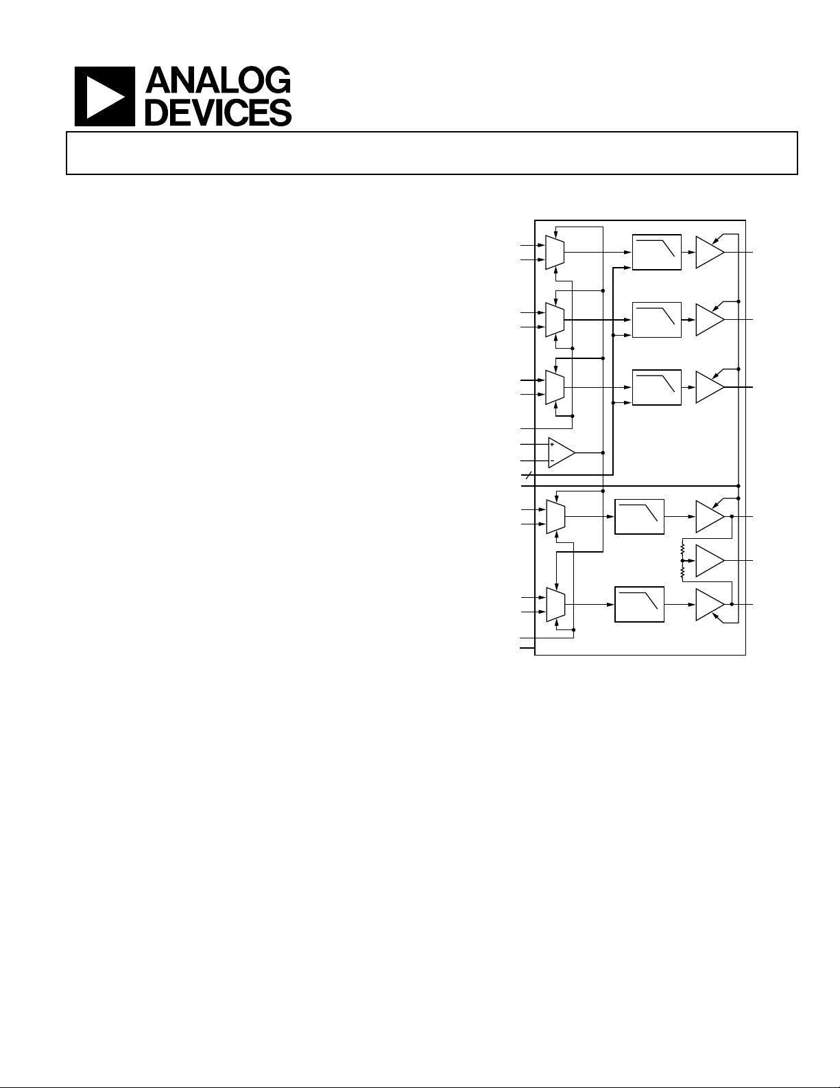
GENERAL DESCRIPTION
The ADA4410-6 is a comprehensive integrated filtering solution
that is carefully designed to give designers the flexibility to
easily filter and drive many types of video signals, including
high definition video. In the GBR/component channels, the
cutoff frequencies of the sixth-order filters can be selected by
two logic pins to obtain four filter combinations that are tuned
for GBR, high definition, and standard definition video. Cutoff
frequencies range from 36 MHz to 9 MHz.
The ADA4410-6 also provides filtering for the legacy standard
S-video and composite video signals. With a differential gain of
0.11% and a differential phase of 0.25°, the ADA4410-6 is an
excellent choice for any composite video (CV) application.
The ADA441-6 offers gain and output offset voltage
adjustments. The gain of the part can be ×2 or ×4, and the
output offset voltage is continuously adjustable up to ±2 V
by applying a differential voltage to an independent offset
control input.
uencies for GBR, HD/SD Y, C, and CV
ADA4410-6
FUNCTIONAL BLOCK DIAGRAM
Y1/G1 IN
Y2/G2 IN
Pb1/B1 IN
Pb2/B2 IN
Pr1/R1 IN
Pr2/R2 IN
HD INPUT SELECT
LEVEL2
LEVEL1
CUTOFF SELECT
GAIN SELECT
Y1 IN
Y2 IN
C1 IN
C2 IN
SD INPUT SELECT
DISABLE
DC
OFFSET
2
9MHz
9MHz
36MHz,
18MHz,
9MHz
36MHz,
18MHz,
9MHz
36MHz,
18MHz,
9MHz
ADA4410-6
Figure 1.
The ADA4410-6 can operate on a single +5 V supply as well as
±5 V supplies. Single-supply operation is ideal for applications
where power consumption is critical. A disable feature allows
for further power conservation.
Dual-supply operation is for applications where the negativegoing excursions of the signal must swing at or below ground
while maintaining excellent video performance. The output
buffers have the ability to drive two 75 Ω terminated loads that
are either dc- or ac-coupled.
The ADA4410-6 is available in a 32-lead LFCSP and operates in
the commercial temperature range of −40°C to +85°C.
×2
×4
×2
×4
×2
×4
×2
×4
×2
×2
×4
Y/G OUT
Pb/B OUT
Pr/R OUT
Y OUT
CV OUT
C OUT
05265-001
The ADA4410-6 offers 2:1 multiplexers on its inputs that can be
used in applications where multiple sources of video exist.
Rev. 0
Information furnished by Analog Devices is believed to be accurate and reliable.
However, no responsibility is assumed by Analog Devices for its use, nor for any
infringements of patents or other rights of third parties that may result from its use.
Specifications subject to change without notice. No license is granted by implication
or otherwise under any patent or patent rights of Analog Devices. Trademarks and
registered trademarks are the property of their respective owners.
One Technology Way, P.O. Box 9106, Norwood, MA 02062-9106, U.S.A.
Tel: 781.329.4700
Fax: 781.326.8703 © 2005 Analog Devices, Inc. All rights reserved.
www.analog.com
Page 2

ADA4410-6
TABLE OF CONTENTS
Specifications..................................................................................... 3
Gain Select................................................................................... 13
Absolute Maximum Ratings............................................................ 7
Thermal Resistance ...................................................................... 7
ESD Caution.................................................................................. 7
Pin Configuration and Function Descriptions............................. 8
Typical Performance Characteristics ............................................. 9
Theory of Operation ...................................................................... 12
Applications..................................................................................... 13
Overview...................................................................................... 13
Multiplexer Select Inputs........................................................... 13
REVISION HISTORY
1/05—Revision 0: Initial Version
Disable ......................................................................................... 13
Cutoff Frequency Selection....................................................... 13
Output DC Offset Control........................................................ 13
Input and Output Coupling ...................................................... 14
Printed Circuit Board Layout ................................................... 14
Video Encoder Reconstruction Filter...................................... 15
Outline Dimensions ....................................................................... 16
Ordering Guide .......................................................................... 16
Rev. 0 | Page 2 of 16
Page 3

ADA4410-6
SPECIFICATIONS
VS = 5 V, @ TA = 25°C, VO = 1.4 V p-p, G = ×2, RL = 150 Ω, unless otherwise noted.
Table 1.
Parameter Test Conditions/Comments Min Typ Max Unit
OVERALL PERFORMANCE
Offset Error Input referred, all channels except CV 10 34 mV
Input referred, CV 12 44 mV
Offset Adjust Range
(see the Output DC Offset Control section)
Input Voltage Range, All Inputs VS− − 0.1 VS+ − 2.0 V
Output Voltage Range, All Outputs IO = 15 mA, positive swing VS+ − 0.5 VS+ − 0.25 V
I
Linear Output Current per Channel 30 mA
Integrated Voltage Noise, Referred to Input All channels except CV 500 µV
Filter Input Bias Current All channels 6.6 9.5 µA
Total Harmonic Distortion at 1 MHz fC = 36 MHz, fC = 18 MHz/fC = 9 MHz 0.01/0.07 %
GBR/YPbPr CHANNEL DYNAMIC PERFORMANCE
−1 dB Bandwidth Cutoff frequency select = 36 MHz 30 MHz
Cutoff frequency select = 18 MHz 15 MHz
Cutoff frequency select = 9 MHz 8 MHz
−3 dB Bandwidth Cutoff frequency select = 36 MHz 34 36 MHz
Cutoff frequency select = 18 MHz 16 18 MHz
Cutoff frequency select = 9 MHz 8 9 MHz
Out-of-Band Rejection f = 75 MHz −27 −32 dB
Crosstalk f = 5 MHz, fC = 36 MHz −68 dB
Input MUX Isolation f = 1 MHz, R
Propagation Delay f = 16 MHz, fC = 36 MHz 20 ns
Group Delay Variation Cutoff frequency select = 36 MHz 8 ns
Cutoff frequency select = 18 MHz 15 ns
Cutoff frequency select = 9 MHz 26 ns
Y/C SD CHANNEL DYNAMIC PERFORMANCE
−1 dB Bandwidth 8 MHz
−3 dB Bandwidth 8 9 MHz
Out-of-Band Rejection f = 27 MHz −54 dB
Propagation Delay f = 1 MHz 70 ns
Group Delay Variation 26 ns
Crosstalk f = 1 MHz −72 dB
Input MUX Isolation f = 1 MHz, R
Y/C, CV OUTPUT VIDEO PERFORMANCE
Differential Gain NTSC 0.09 %
Differential Phase NTSC 0.37 Degrees
CONTROL INPUT PERFORMANCE
Input Logic 0 Voltage All inputs except DISABLE 0.8 V
Input Logic 1 Voltage All inputs except DISABLE 2.0 V
Input Bias Current All inputs except DISABLE 7 9.5 µA
DISABLE PERFORMANCE
DISABLE Assert Voltage VS+ − 0.5 V
DISABLE Assert Time 100 ns
DISABLE De-Assert Time 130 ns
DISABLE Input Bias Current 12 20 µA
Input-to-Output Isolation—Disabled 100 dB
Input Referred ±500 mV
= 15 mA, negative swing VS− + 0.4 VS- + 0.12 V
O
= 300 Ω 86 dB
SOURCE
= 75 Ω 77 dB
SOURCE
rms
Rev. 0 | Page 3 of 16
Page 4

ADA4410-6
Parameter Test Conditions/Comments Min Typ Max Unit
POWER SUPPLY
Operating Range 4.5 12 V
Quiescent Current 81 92 mA
Quiescent Current—Disabled 15 150 µA
PSRR, Positive Supply All channels except CV 60 72 dB
CV channel 54 66 dB
PSRR, Negative Supply All channels except CV 55 62 dB
CV channel 49 56 dB
Rev. 0 | Page 4 of 16
Page 5

ADA4410-6
VS = ±5 V, @ TA = 25°C, VO = 1.4 V p-p, G = ×2, RL = 150 Ω, unless otherwise noted.
Table 2.
Parameter Test Conditions/Comments Min Typ Max Unit
OVERALL PERFORMANCE
Offset Error Input referred, all channels except CV 14 35 mV
Input referred, CV 15 48 mV
Offset Adjust Range
(see the Output DC Offset Control section)
Input Voltage Range, All Inputs VS− − 0.1 VS+ − 2.0 V
Output Voltage Range, All Outputs IO = 30 mA, positive swing VS+ − 0.6 VS+ − 0.3 V
I
Linear Output Current per Channel 30 mA
Integrated Voltage Noise, Referred to Input All channels except CV 500 µV
Filter Input Bias Current All channels 6.3 9.5 µA
Total Harmonic Distortion at 1 MHz fC = 36 MHz, fC = 18 MHz/fC = 9 MHz 0.01/0.07 %
GBR/YPbPr CHANNEL DYNAMIC PERFORMANCE
−1 dB Bandwidth Cutoff frequency select = 36 MHz 28 MHz
Cutoff frequency select = 18 MHz 15 MHz
Cutoff frequency select = 9 MHz 8 MHz
−3 dB Bandwidth Cutoff frequency select = 36 MHz 33.5 35.5 MHz
Cutoff frequency select = 18 MHz 16 18 MHz
Cutoff frequency select = 9 MHz 8 9.5 MHz
Out-of-Band Rejection f = 75 MHz −27 −32 dB
Crosstalk f = 5 MHz, fC = 36 MHz −68 dB
Input MUX Isolation f = 1 MHz, R
Propagation Delay f = 5 MHz, fC = 36 MHz 21 ns
Group Delay Variation Cutoff frequency select = 36 MHz 6 ns
Cutoff frequency select = 18 MHz 13 ns
Cutoff frequency select = 9 MHz 23 ns
Y/C SD CHANNEL DYNAMIC PERFORMANCE
−1 dB Bandwidth 8 MHz
−3 dB Bandwidth 8 9 MHz
Out-of-Band Rejection f = 27 MHz −51 dB
Propagation Delay f = 1 MHz 67 ns
Group Delay Variation 22.5 ns
Crosstalk f = 1 MHz −72 dB
Input MUX Isolation f = 1 MHz, R
Y/C, CV OUTPUT VIDEO PERFORMANCE
Differential Gain NTSC 0.11 %
Differential Phase NTSC 0.25 Degrees
CONTROL INPUT PERFORMANCE
Input Logic 0 Voltage All inputs except DISABLE 0.8 V
Input Logic 1 Voltage All inputs except DISABLE 2.0 V
Input Bias Current All inputs except DISABLE 7 9.5 µA
DISABLE PERFORMANCE
DISABLE Assert Voltage VS+ − 0.5 V
DISABLE Assert Time 75 ns
DISABLE De-Assert Time 125 ns
DISABLE Input Bias Current 35 45 µA
Input-to-Output Isolation—Disabled 100 dB
Input Referred ±500 mV
= 30 mA, negative swing VS− + 0.6 VS− + 0.3 V
O
rms
= 300 Ω 86 dB
SOURCE
= 75 Ω 77 dB
SOURCE
Rev. 0 | Page 5 of 16
Page 6

ADA4410-6
Parameter Test Conditions/Comments Min Typ Max Unit
POWER SUPPLY
Operating Range 4.5 12 V
Quiescent Current 85 95 mA
Quiescent Current—Disabled 15 150 µA
PSRR, Positive Supply All channels except CV 60 72 dB
CV channel 54 66 dB
PSRR, Negative Supply All channels except CV 55 62 dB
CV channel 49 56 dB
Rev. 0 | Page 6 of 16
Page 7

ADA4410-6
ABSOLUTE MAXIMUM RATINGS
Table 3.
Parameter Rating
Supply Voltage 12 V
Power Dissipation See Figure 2
Storage Temperature –65°C to +125°C
Operating Temperature Range –40°C to +85°C
Lead Temperature Range (Soldering 10 sec) 300°C
Junction Temperature 150°C
The power dissipated in the package (P
quiescent power dissipation and the power dissipated in the
package due to the load drive for all outputs. The quiescent
power is the voltage between the supply pins (V
quiescent current (I
depends upon the particular application. For each output, the
power due to load drive is calculated by multiplying the load
current by the associated voltage drop across the device. The
power dissipated due to all of the loads is equal to the sum of
Stresses above those listed under Absolute Maximum Ratings
may cause permanent damage to the device. This is a stress
the power dissipations due to each individual load. RMS
voltages and currents must be used in these calculations.
rating only; functional operation of the device at these or any
other conditions above those indicated in the operational
section of this specification is not implied. Exposure to absolute
maximum rating conditions for extended periods may affect
device reliability.
Airflow increases heat dissipation, effectively reducing θ
Also, more metal directly in contact with the package leads
from metal traces, through-holes, ground, and power planes
reduces the θ
. The exposed paddle on the underside of the
JA
package must be soldered to a pad on the PCB surface that is
THERMAL RESISTANCE
θJA is specified for the worst-case conditions, that is, θJA is
specified for a device soldered in the circuit board with its
exposed paddle soldered to a pad on the PCB surface that is
thermally connected to a copper plane.
Table 4. Thermal Resistance
Package Type θ
5 mm × 5 mm, 32-Lead LFCSP 43 5.1 °C/W
Maximum Power Dissipation
θ
JA
Unit
JC
thermally connected to a copper plane in order to achieve the
specified θ
.
JA
Figure 2 shows the maximum safe power dissipation in the
package vs. the ambient temperature for the 32-lead LFCSP
(43°C/W) on a JEDEC standard 4-layer board with the
underside paddle soldered to a pad that is thermally connected
to a PCB plane. θ
4.5
4.0
The maximum safe power dissipation in the ADA4410-6
package is limited by the associated rise in junction temperature
) on the die. At approximately 150°C, which is the glass
(T
J
transition temperature, the plastic changes its properties.
Even temporarily exceeding this temperature limit may change
3.5
3.0
2.5
the stresses that the package exerts on the die, permanently
shifting the parametric performance of the ADA4410-6.
Exceeding a junction temperature of 150°C for an extended
period of time can result in changes in the silicon devices
potentially causing failure.
2.0
1.5
MAXIMUM POWER DISSIPATION (W)
1.0
–40 –20 0 20 40 60
Figure 2. Maximum Power Dissipation vs. Temperature for a 4-Layer Board
). The power dissipated due to load drive
S
values are approximations.
JA
AMBIENT TEMPERATURE (°C)
) is the sum of the
D
LFCSP
) times the
S
80
.
JA
05265-002
ESD CAUTION
ESD (electrostatic discharge) sensitive device. Electrostatic charges as high as 4000 V readily accumulate
on the human body and test equipment and can discharge without detection. Although this product features
proprietary ESD protection circuitry, permanent damage may occur on devices subjected to high energy
electrostatic discharges. Therefore, proper ESD precautions are recommended to avoid performance
degradation or loss of functionality.
Rev. 0 | Page 7 of 16
Page 8

ADA4410-6
PIN CONFIGURATION AND FUNCTION DESCRIPTIONS
1
PIN 1
INDICATOR
ADA4410-6
(Not to Scale)
8
Figure 3. 32-Lead LFCSP, Top View
2532
24
17
169
05265-003
Table 5. Pin Function Descriptions
Pin No. Name Description
1 Pb1/B1_HD Channel 1 Pb/B High Definition Input
2 GND Signal Ground Reference
3 Pr1/R1_HD Channel 1 Pr/R High Definition Input
4 F_SEL_A Filter Cutoff Select Input A
5 F_SEL_B Filter Cutoff Select Input B
6 Y2/G2_HD Channel 2 Y/G High Definition Input
7 GND Signal Ground Reference
8 Pb2/B2_HD Channel 2 Pb/B High Definition Input
9 GND Signal Ground Reference
10 Pr2/R2_HD Channel 2 Pr/R High Definition Input
11 MUX_SD Standard Definition Input MUX Select Line
12 Y1_SD Channel 1 Y Standard Definition Input
13 Y2_SD Channel 2 Y Standard Definition Input
14 C1_SD Channel 1 C Standard Definition Input
15 C2_SD Channel 2 C Standard Definition Input
16 VCC Positive Power Supply
17 VEE Negative Power Supply
18 CV_OUT Composite Video Output
19 C_SD_OUT C Standard Definition Output
20 Y_SD_OUT Y Standard Definition Output
21 G_SEL Gain Select
22 Pr/R_HD_OUT Pr/R High Definition Output
23 Pb/B_HD_OUT Pb/B High Definition Output
24 Y/G_HD_OUT Y/G High Definition Output
25 VEE Negative Power Supply
26 VCC Positive Power Supply
27 DISABLE Disable/Power Down/Logic Reference
28 LEVEL2 DC Level Adjust Pin 2
29 LEVEL1 DC Level Adjust Pin 1
30 MUX_HD High Definition Input MUX Select Line
31 Y1/G1_HD Channel 1 Y/G High Definition Input
32 GND Signal Ground Reference
Rev. 0 | Page 8 of 16
Page 9

ADA4410-6
TYPICAL PERFORMANCE CHARACTERISTICS
Unless otherwise noted, G = ×2, RL = 150 Ω, VO = 1.4 V p-p, VS = 5 V, TA = 25°C.
9
6
3
0
–3
–6
–9
–12
–15
–18
–21
BLACK LINES: VS = +5V
–24
GAIN (dB)
GRAY LINES: V
–27
–30
–33
–36
–39
–42
–45
–48
1 10 100
= ±5V
S
FREQUENCY (MHz)
F
C
= 9MHz
F
= 18MHz
C
F
= 36MHz
C
05265-004
Figure 4. Frequency Response vs. Power Supply and Cutoff Frequency (G = ×2)
15
12
9
6
3
0
–3
–6
–9
–12
BLACK LINES: VS = +5V
–15
GRAY LINES: V
–18
GAIN (dB)
–21
–24
–27
–30
–33
–36
–39
–42
–45
1 10 100
= ±5V
S
FREQUENCY (MHz)
F
C
= 9MHz
F
= 18MHz
C
F
= 36MHz
C
05265-006
Figure 7. Frequency Response vs. Power Supply and Cutoff Frequency (G = ×4)
6.5
6.0
BLACK LINES: VS = +5V
GRAY LINES: V
5.5
5.0
4.5
GAIN (dB)
4.0
3.5
3.0
= ±5V
S
1 10 100
FREQUENCY (MHz)
= 9MHz
F
C
F
F
= 18MHz
C
= 36MHz
C
05265-005
Figure 5. Frequency Response Flatness vs. Cutoff Frequency (G = ×2)
9
6
3
0
–3
–6
–9
–12
–15
–18
–21
–24
GAIN (dB)
–27
–30
–33
–36
–39
–42
–45
–48
1 10 100
FREQUENCY (MHz)
FC = 9MHz
F
= 18MHz
C
F
0.1V p-p
1.4V p-p
2.0V p-p
= 36MHz
C
05265-053
Figure 6. Frequency Response vs. Cutoff Frequency and Output Amplitude
12.5
12.0
BLACK LINES: VS = +5V
GRAY LINES: V
11.5
11.0
10.5
GAIN (dB)
10.0
9.5
9.0
= ±5V
S
1 10 100
FREQUENCY (MHz)
F
= 9MHz
C
F
F
= 18MHz
C
= 36MHz
C
Figure 8. Frequency Response Flatness vs. Cutoff Frequency (G = ×4)
9
6
3
0
–3
–6
–9
–12
–15
–18
–21
–24
GAIN (dB)
–27
–30
–33
–36
–39
–42
–45
–48
1 10010
FC = 9MHz
+85°C
+25°C
–40°C
FREQUENCY (MHz)
= 18MHz
F
C
F
= 36MHz
C
Figure 9. Frequency Response vs. Temperature and Cutoff Frequency
05265-007
05265-017
Rev. 0 | Page 9 of 16
Page 10

ADA4410-6
100
BLACK LINES: VS = +5V
GRAY LINES: V
90
FC = 9MHz
80
70
60
50
40
GROUP DELAY (ns)
30
20
10
1 10 100
Figure 10. Group D elay vs. Frequency, Power Supply, and Cutoff Frequency
= ±5V
S
FC = 18MHz
FC = 36MHz
FREQUENCY (MHz)
05265-008
–60
BANDWIDTH 100kHz TO 4.2MHz
NTC-7 WEIGHT
–65
–70
–75
–80
–85
–90
NOISE (dB)
–95
–100
–105
–110
01 432
Figure 13. CV Noise Spectrum
FREQUENCY (MHz)
05265-020
5
–40
–50
–60
–70
–80
–90
R
–100
SOURCE
CROSSTALK REFERRED TO INPUT (dB)
Y1, Pb1 SOURCE CHANNELS
Pr1 RECEPTOR CHANNEL
–110
0.1 1 10010
FC = 9MHz
= 300Ω
= 18MHz
F
C
FREQUENCY (MHz)
= 36MHz
F
C
Figure 11. HD Channel Crossta lk vs. Frequenc y and Cutoff Frequen cy
–40
R
= 300Ω
SOURCE
UNSELECTED MUX IS DRIVEN
–50
–60
–70
–80
–90
–100
MUX ISOLATION REFERRED TO INPUT (dB)
–110
0.1 1 10010
F
= 18MHz
C
= 9MHz
F
C
FREQUENCY (MHz)
FC = 36MHz
Figure 12. HD MUX Isolation vs. Frequency and Cutoff Frequency
05265-018
05265-013
–40
R
= 300Ω
SOURCE
MUX INPUT 2 SELECTED
–50
–60
–70
–80
–90
–100
CROSSTALK REFERRED TO INPUT (dB)
–110
0.1 1 10010
Y1, C1 SOURCE CHANNELS
Y2 RECEPTOR CHANNEL
C2 SOURCE CHANNELS
Y2 RECEPTOR CHANNEL
FREQUENCY (MHz)
Figure 14. SD Channel Crosstalk vs. Frequency
–40
UNSELECTED MUX IS DRIVEN
–50
–60
R
= 300Ω
SOURCE
–70
–80
R
= 75Ω
–90
–100
MUX ISOLATION REFERRED TO INPUT (dB)
–110
0.1 1 10010
SOURCE
FREQUENCY (MHz)
Figure 15. SD MUX Isolation vs. Frequency and Source Resistance
05265-019
05265-014
Rev. 0 | Page 10 of 16
Page 11

ADA4410-6
–5
–5
–15
–25
–35
–45
–55
PSRR REFERRED TO INPUT (dB)
–65
–75
0.1 1 10010
F
= 18MHz
C
FC = 9MHz
F
FREQUENCY (MHz)
= 36MHz
C
Figure 16. Positive Supply PSRR vs. Frequency and Cutoff Frequency
3.5
3.3
3.1
F
= 36MHz
C
2.9
2.7
2.5
2.3
2.1
OUTPUT VOLTAGE (V)
1.9
1.7
1.5
= 18MHz
F
C
= 9MHz
F
C
200ns/DIV
Figure 17. Transient Response vs. Cutoff Frequency (G = ×2)
3.5
3.3
3.1
2.9
2.7
2.5
2.3
2.1
OUTPUT VOLTAGE (V)
1.9
1.7
1.5
t = 0
1% (57ns)
2× INPUT
ERROR = 2
0.5% (65ns)
OUTPUT
×
INPUT – OUTPUT (0.5%/DIV)
50ns/DIV
Figure 18. Settling Time
05265-015
05265-009
05265-010
–15
= 18MHz
F
C
FC = 9MHz
= 36MHz
F
C
FREQUENCY (MHz)
–25
–35
–45
–55
PSRR REFERRED TO INPUT (dB)
–65
–75
0.1 1 10010
Figure 19. Negat ive Supply PSRR vs. Frequenc y and Cutoff Frequen cy
3.5
3.3
3.1
F
= 36MHz
C
2.9
2.7
2.5
2.3
2.1
OUTPUT VOLTAGE (V)
1.9
1.7
1.5
= 18MHz
F
C
F
= 9MHz
C
G = 4
V
= 1.4V p-p
O
200ns/DIV
Figure 20. Transient Response vs. Cutoff Frequency (G = ×4)
6
5
4
F
3
2
1
OUTPUT VOLTAGE (V)
0
–1
C
= 36MHz
2
×
INPUT VOLTAGE
= 18MHz
F
C
FC = 9MHz
200ns/DIV
Figure 21. Overdrive Recovery vs. Cutoff Frequency
05265-016
05265-011
05265-012
NETWORK
ANALYZER Tx
50Ω 118Ω
MINIMUM-LOSS MATCHING NETWORK LOSS CALIBRATED OUT
= 150Ω
R
L
DUT
50Ω 86.6Ω
NETWORK
ANALYZER Rx
50Ω
Figure 22. Basic Test Circuit for Swept Frequency Measurements
Rev. 0 | Page 11 of 16
05265-051
Page 12

ADA4410-6
THEORY OF OPERATION
The ADA4410-6 is an integrated video filtering and driving
solution that offers variable bandwidth to meet the needs of
several different video formats. There are a total of five filter
sections, three for component video and two for Y/C and
composite video. The component video filters have switchable
bandwidths for standard definition interlaced, progressive, and
high definition systems. The Y/C channels have fixed 9 MHz
3 dB cutoff frequencies and include a summing circuit that
feeds an additional buffer for a composite video output. Each
filter section has a sixth-order Butterworth response that
includes group delay optimization. The group delay variation
from 100 kHz to 36 MHz in the 36 MHz section is 8 ns, which
produces a fast settling pulse response.
The ADA4410-6 is designed to operate in many different video
environments. The supply range is 5 V to 12 V, single supply or
dual supply, and requires a relatively low quiescent current of
15 mA per channel. In single-supply applications, the PSRR is
greater than 70 dB, providing excellent rejection in systems with
supplies that are noisy or underregulated. In applications where
power consumption is critical, the part can be powered down to
draw less than 10 µA by pulling the DISABLE pin to the most
positive rail. The ADA4410-6 is also well-suited for high
encoding frequency applications because it maintains a stopband attenuation of 50 dB beyond 200 MHz.
The ADA4410-6 is intended to take dc-coupled inputs from an
encoder or other ground referenced video signals. The
ADA4410-6 input is high impedance. No minimum or
maximum input termination is required, although, input
terminations above 1 kΩ can degrade crosstalk performance at
high frequencies. No clamping is provided internally. For
applications where dc restoration is required, dual supplies
work best. Using a termination resistance of less than a few
hundred ohms to ground on the inputs and suitably adjusting
the level shift circuitry provides precise placement of the output
voltage.
For single-supply applications (V
range extends from 100 mV below ground to within 2.0 V of
the most positive supply. Each filter section has a 2:1 input
multiplexer that includes level-shifting circuitry. The levelshifting circuitry adds a dc component to ground-referenced
input signals so that they can be reproduced accurately without
the output buffers hitting the negative rail. Because the filters
have negative rail input and rail-to-rail output, dc level shifting
is generally not necessary, unless accuracy greater than that of
the saturated output of the driver is required at the most
negative edge. This varies with load but is typically 100 mV
in a dc-coupled, single-supply application. If ac coupling is
used, the saturated output level is higher because the drivers
have to sink more current on the low side. If dual supplies are
used (V
applications, the level shifting circuitry can be used to take a
ground referenced signal and put the blanking level at ground
while the sync level is below ground.
The output drivers on the ADA4410-6 have rail-to-rail output
capabilities. They provide either 6 dB or 12 dB of gain with
respect to the ground pins. Gain is controlled by the external
gain select pin. Each output is capable of driving two ac- or dccoupled 75 Ω source-terminated loads. If a large dc output level
is required while driving two loads, ac coupling should be used
to limit the power dissipation.
Input MUX isolation is primarily a function of the source
resistance driving into the ADA4410-6. Higher resistances
result in lower isolation over frequency, while a low source
resistance, such as 75 Ω, has the best isolation performance. In
the SD channels, the isolation variation is most pronounced due
to the stray capacitance that exists between the adjacent input
pins. The HD input pins are not adjacent; therefore, this effect is
less pronounced on the HD channels. See Figure 15 for a
perform-ance comparison of the different source resistances
feeding the SD inputs.
< GND), no level shifting is required. In dual-supply
S−
= GND), the input voltage
S−
Rev. 0 | Page 12 of 16
Page 13

ADA4410-6
APPLICATIONS
OVERVIEW
With its high impedance multiplexed inputs and high output
drive, the ADA4410-6 is ideally suited to video reconstruction
and antialias filtering applications. The high impedance inputs
give designers flexibility with regard to how the input signals
are terminated. Devices with DAC outputs that feed the
ADA4410-6 can be loaded in whatever resistance provides
the best performance, and devices with voltage outputs can be
optimally terminated as well. The ADA4410-6 outputs can each
drive up to two source-terminated 75 Ω loads and can therefore
directly drive the outputs from set-top boxes, DVD players, and
the like without the need for a separate output buffer.
Binary control inputs are provided to select cutoff frequency,
throughput gain, and input signal. These inputs are compatible
with 3 V and 5 V TTL and CMOS logic levels, referenced to
GND. The disable feature is asserted by pulling the DISABLE
pin to the positive supply.
A differential input, comprising of the LEVEL1 and LEVEL2
inputs, controls the dc level at the output pins. The output offset
is nominally calculated as
OS
where
LEVEL2 and LEVEL1 are the voltages applied to the
respective inputs and
−= (1)
G is throughput gain.
))(()( GLEVEL1LEVEL2OUTV
MULTIPLEXER SELECT INPUTS
Selection between the two multiplexer inputs is controlled by
the logic signals applied to the MUX_SD and MUX_HD inputs.
The MUX_SD input controls the standard definition (SD)
inputs, and the MUX_HD input controls the high definition
(HD) inputs. Table 6 summarizes the multiplexer operation.
GAIN SELECT
The throughput gain of the ADA4410-6 signal paths can
either be ×2 or ×4. Gain selection is controlled by the logic
signal applied to the G_SEL pin. Table 6 summarizes how the
gain is selected.
DISABLE
The ADA4410-6 includes a disable feature that can be used
to save power when a particular device is not in use. As
indicated in the Overview section, the disable feature is
asserted by pulling the DISABLE pin to the positive supply.
Table 6 summarizes the disable feature operation. The
DISABLE pin also functions as a reference level for the logic
inputs and, therefore, must be connected to ground when the
device is not disabled.
Table 6. Logic Pin Function Description
DISABLE MUX_HD MUX_SD G_SEL
VS+ =
Disabled
GND =
Enabled
1 = HD Channel 1
Selected
0 = HD Channel 2
Selected
1 = SD Channel 1
Selected
0 = SD Channel 2
Selected
1 = ×4
Gain
0 = ×2
Gain
CUTOFF FREQUENCY SELECTION
Four combinations of cutoff frequencies are provided for the
HD video signals. The cutoff frequencies have been selected to
correspond with the most commonly deployed HD scanning
systems. Selection between the cutoff frequency combinations is
controlled by the logic signals applied to the F_SEL_A and
F_SEL_B inputs. Table 7 summarizes cutoff frequency selection.
Table 7. Filter Cutoff Frequency Selection
Y/G Cutoff
F_SEL_A F_SEL_B
0 0 36 36 36
0 1 36 18 18
1 0 18 18 18
1 1 9 9 9
(MHz)
Pb/B Cutoff
(MHz)
Pr/R Cutoff
(MHz)
OUTPUT DC OFFSET CONTROL
The LEVEL1 and LEVEL2 inputs work as a differential
input-referred output offset control. In other words, the output
offset voltage of a given channel (with the exception of the CV
channel) is equal to the difference in voltage between the
LEVEL2 and LEVEL1 inputs, multiplied by the overall filter
gain. This relationship is expressed in Equation 1. For example,
with the G_SEL input set for ×2 gain, setting LEVEL2 to
300 mV and LEVEL1 to 0 V shifts the offset voltages at the
ADA4401-6 outputs to 600 mV. This particular setting can be
used in most single-supply applications to keep the output
swings safely above the negative supply rail.
The CV output is developed by passively summing the Y and C
outputs that have passed through their respective output gain
stages, then multiplying this sum by a factor of two to obtain
the output (see Figure 1). The offset of this output is therefore
equal to two times that of the other outputs. Because of this, in
many cases it is necessary to ac-couple the CV output or ensure
that it is connected to an input that is ac-coupled. This is
generally not an issue because it is common practice to employ
ac coupling on composite video inputs.
The maximum differential voltage that can be applied across the
LEVEL1 and LEVEL2 inputs is ±500 mV. From a single-ended
standpoint, the LEVEL1 and LEVEL2 inputs have the same
range as the filter inputs. See the Specifications tables for the
limits. The LEVEL1 and LEVEL2 inputs must each be bypassed
to GND with a 0.1 µF ceramic capacitor.
Rev. 0 | Page 13 of 16
Page 14

ADA4410-6
In single-supply applications, a positive output offset must be
applied to keep the negative-most excursions of the output
signals above the specified minimum output swing limit.
Figure 23 and Figure 24 illustrate several ways to use the
LEVEL1 and LEVEL2 inputs. Figure 23 shows an example of
how to generate fully adjustable LEVEL1 and LEVEL2 voltages
from ±5 V supplies. Figure 24 illustrates an effective way to
produce a 600 mV output offset voltage in a single-supply
application. Although the LEVEL1 input could simply be
connected to GND, Figure 24 includes bypassed resistive
voltage dividers for each input so that the input levels can be
changed, if necessary. Additionally, many in-circuit testers
require that I/O signals not be tied directly to the supplies or
GND. DNP indicates do not populate.
DUAL SUPPLY
+5V
9.53kΩ
1kΩ
9.53kΩ
–5V
+5V
9.09kΩ
1kΩ
Figure 23. Generating Fully Adjustable Output Offsets
LEVEL1
0.1µF
SINGLE SUPPLY
LEVEL1
0.1µF
+5V
DNP
LEVEL1
0Ω
Figure 24. Setting Output Offsets to 600 mV on a Single Supply
DNP
9.53kΩ
1kΩ
9.53kΩ
9.09kΩ
1kΩ
10kΩ
634Ω
+5V
+5V
–5V
+5V
0.1µF
0.1µF
0.1µF
LEVEL2
LEVEL2
LEVEL2
05265-048
05265-049
INPUT AND OUTPUT COUPLING
Inputs to the ADA4410-6 are normally dc-coupled. Ac coupling
the inputs is not recommended; however, if ac coupling is
necessary, a suitable resistive network must be provided
following the ac coupling element to provide proper level
shifting and bias currents for the ADA4410-6 input stages.
The ADA4410-6 outputs can be either ac- or dc-coupled. As
discussed in the Output DC Offset Control section, the CV
output offset is different than the other outputs and is generally
ac-coupled.
PRINTED CIRCUIT BOARD LAYOUT
As with all high speed applications, attention to printed
circuit board layout is of paramount importance. Standard high
speed layout practices should be adhered to when designing
with the ADA4410-6. A solid ground plane is recommended,
and surface-mount ceramic power supply decoupling capacitors
should be placed as close as possible to the supply pins. All of
the ADA4410-6 GND pins should be connected to the ground
plane with traces that are as short as possible. Controlled
impedance traces of the shortest length possible should be used
to connect to the signal I/O pins and should not pass over any
voids in the ground plane. A 75 Ω impedance level is typically
used in video applications. All signal outputs of the ADA4410-6
should include series termination resistors when driving
transmission lines.
When the ADA4410-6 receives its inputs from a device
with current outputs, the required load resistor value for the
output current is most often different from the characteristic
impedance of the signal traces. In this case, if the interconnections are sufficiently short (<< 0.1 wavelength), the trace
does not have to be terminated in its characteristic impedance.
Figure 25 shows an example in which the ADA4410-6 input
originates from DACs that require 300 Ω load resistors. Traces
of 75 Ω can be used in this instance, provided their lengths are
an inch or two at the most. This is easily achieved because the
ADA4410-6 and the device feeding it are usually adjacent to
each other, and connections can be made that are less than one
inch in length.
Rev. 0 | Page 14 of 16
Page 15

ADA4410-6
DEVICE
ADDRESS
SELECT
5kΩ
5kΩ5kΩ
CHANNEL 2
VIDEO INPUTS
5V
(ANALOG)
0.1µF
26
VCC
CV_OUT
Y_SD_OUT
C_SD_OUT
VEE
17, 25
0.1µF
75Ω
18
220µF
75Ω
20
220µF
75Ω
19
0.1µF
75Ω
24
220µF
75Ω
23
220µF
75Ω
22
220µF
2
I
BUS
DNP*
C
0Ω
10kΩ
634Ω
DNP*
BINARY
CONTROL
INPUTS
28
LEVEL2
0.1µF
29
LEVEL1
27
DISABLE
21
G_SEL
11
MUX_SD
30
MUX_HD
4
F_SEL_A
5
F_SEL_B
12
Y1_SD
13
Y2_SD
14
C1_SD
15
C2_SD
31
Y1/G1_HD
6
Y2/G2_HD
1
Pb1/B1_HD
8
Pb2/B2_HD
3
Pr1/R1_HD
10
Pr2/R2_HD
GND
*DO NOT POPULATE
16
VCC
ADA4410-6
2, 7, 9, 32
Y/G_HD_OUT
Pb/B_HD_OUT
Pr/R_HD_OUT
VIDEO ENCODER RECONSTRUCTION FILTER
The ADA4410-6 is easily applied as a reconstruction filter at the
DAC outputs of a video encoder. Figure 25 illustrates how to
use the ADA4410-6 in this type of application with an
ADV7314 video encoder in a single-supply application with accoupled outputs.
NOTE: EACH POWER SUPPLY PIN MUST HAVE ITS OWN DECOUPLING NETWORK
1.1kΩ
0.01µF 0.1µF
AD1580
4.7kΩ
RESET
820pF
4.7kΩ
DIGITAL
BUSES
MULTIFUNCTIONAL
VIDEO
PIXEL
CLOCKS
SYNC AND
BLANKING
SIGNALS
INPUT
14-18, 26-30
51-55, 58-62
0.1µF
4.7µF
3.5pF
2-9, 12, 13
2.5V
(ANALOG)
V
AA
46
V
REF
33
RESET
+
34
EXT_LF
Y9–Y0
C9–C0
S9–S0
32
CLKIN_A
63
CLKIN_B
23
P_HSYNC
24
P_VSYNC
25
P_BLANK
50
S_HSYNC
49
S_VSYNC
48
S_BLANK
31
RTC_SCR_TR
2.5V
(DIGITAL)
V
AGNDDGNDGND_IO
10, 56364541
DD
V
DD_IO
SCLK
ALSB
DAC A
DAC B
DAC C
DAC D
DAC E
DAC F
R
R
0.01µF
I2C
SDA
SET1
SET2
1
19
22
21
20
44
43
42
39
38
37
47
35
0.1µF 0.1µF
COMP1 COMP2
ADV7314
64 11, 57 40
Figure 25. The ADA4410-6 Applied as a Reconstruction Filter Following the ADV7314
0.1µF
5kΩ
100Ω
100Ω
NC
2.5V/3.3V
(DIGITAL I/O)
0.01µF
300Ω
300Ω
300Ω
300Ω
300Ω
3.04kΩ
3.04kΩ
0.1µF
5265-050
Rev. 0 | Page 15 of 16
Page 16

ADA4410-6
OUTLINE DIMENSIONS
0.08
0.60 MAX
25
24
EXPOSED
PAD
(BOTTOM VIEW)
17
16
32
1
8
9
3.50 REF
PIN 1
INDICATOR
3.45
3.30 SQ
3.15
0.25 MIN
PIN 1
INDICATOR
1.00
0.85
0.80
12° MAX
SEATING
PLANE
5.00
BSC SQ
TOP
VIEW
0.80 MAX
0.65 TYP
0.30
0.23
0.18
COMPLIANT TO JEDEC STANDARDS MO-220-VHHD-2
4.75
BSC SQ
0.20 REF
0.05 MAX
0.02 NOM
0.60 MAX
0.50
BSC
0.50
0.40
0.30
COPLANARITY
Figure 26. 32-Lead Lead Frame Chip Scale Package [VQ_LFCSP]
5 mm × 5 mm Body, Very Thin Quad (CP-32-3)
Dimensions shown in millimeters
ORDERING GUIDE
Model Temperature Range Package Description Package Option
ADA4410-6ACPZ-R2
ADA4410-6ACPZ-R71 –40°C to +85°C 32-Lead Lead Frame Chip Scale Package (VQ_LFCSP) CP-32-3
ADA4410-6ACPZ-RL1 –40°C to +85°C 32-Lead Lead Frame Chip Scale Package (VQ_LFCSP) CP-32-3
1
Z = Pb-free part.
1
–40°C to +85°C 32-Lead Lead Frame Chip Scale Package (VQ_LFCSP) CP-32-3
© 2005 Analog Devices, Inc. All rights reserved. Trademarks and
registered trademarks are the property of their respective owners.
D05265–0–1/05(0)
Rev. 0 | Page 16 of 16
 Loading...