

Page 1
O
www.BDTIC.com/ADI
Tiny, Low Power JFET-Input Op Amp
FEATURES
Low input bias current: 50 pA maximum
Offset voltage
1.5 mV maximum for ADA4062-2 B grade
2.5 mV maximum for ADA4062-2 A grade
Offset voltage drift: 4 µV/°C typical
Slew rate: 3.3 V/s typical
CMRR: 90 dB typical
Low supply current: 165 µA typical
High input impedance
Unity-gain stable
Packaging: SOIC, MSOP
APPLICATIONS
Power control and monitoring
Active filters
Industrial/process control
Body probe electronics
Data acquisition
Integrators
Input buffering
GENERAL DESCRIPTION
The ADA4062-2 is a dual JFET-input amplifier with industryleading performance. It offers lower power, offset voltage, drift
and ultralow bias current. The ADA4062-2 B grade features typical
low offset voltage of 0.5 mV, offset drift of 4 μV/°C, and bias current
of 2 pA. The ADA4062-2 is ideal for various applications, including
process control, industrial and instrumentation equipment, active
filtering, data conversion, buffering, and power control and
monitoring. With a low supply current of 165 μA per amplifier,
it is also very well suited for lower power applications. The
ADA4062-2 is specified for the extended industrial temperature
range of −40°C to +125°C and is available in lead-free SOIC and
MSOP packages.
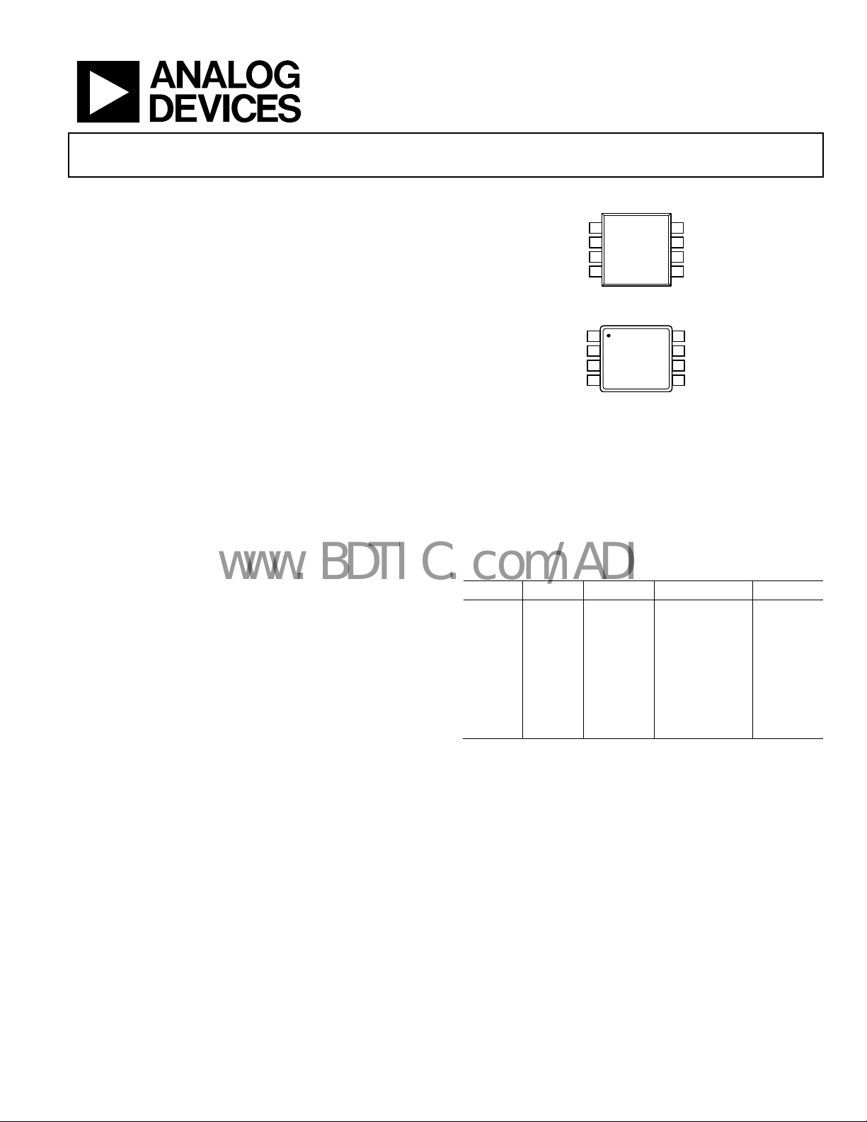
ADA4062-2
PIN CONFIGURATIONS
OUT A
1
ADA4062-2
–IN A
2
+IN A
Figure 1. 8-Lead Narrow-Body SOIC
UT A
–IN A
+IN A
TOP VIEW
3
(Not to Scale)
4
V–
1
ADA4062-2
2
TOP VIEW
3
(Not to Scale)
V–
4
Figure 2. 8-Lead MSOP
Table 1. Low Power Op Amps
Supply 40 V 36 V 12 V to 16 V 5 V
Single OP97 AD820 AD8641 AD8541
AD8663
Dual OP297 OP282 AD8642 AD8542
AD8682 AD8667
AD822
Quad OP497 OP482 AD8643 AD8544
AD8684 AD8669
AD824
8
7
6
5
8
7
6
5
V+
OUT B
–IN B
+IN B
V+
OUT B
–IN B
+IN B
07670-001
7670-002
Rev. 0
Information furnished by Analog Devices is believed to be accurate and reliable. However, no
responsibility is assumed by Analog Devices for its use, nor for any infringements of patents or other
rights of third parties that may result from its use. Specifications subject to change without notice. No
license is granted by implication or otherwise under any patent or patent rights of Analog Devices.
Trademarks and registered trademarks are the property of their respective owners.
One Technology Way, P.O. Box 9106, Norwood, MA 02062-9106, U.S.A.
Tel: 781.329.4700 www.analog.com
Fax: 781.461.3113 ©2008 Analog Devices, Inc. All rights reserved.
Page 2

ADA4062-2
www.BDTIC.com/ADI
TABLE OF CONTENTS
Features .............................................................................................. 1
Applications ....................................................................................... 1
Pin Configurations ........................................................................... 1
General Description ......................................................................... 1
Revision History ............................................................................... 2
Specifications ..................................................................................... 3
Electrical Characteristics ............................................................. 3
Absolute Maximum Ratings ............................................................ 4
Thermal Resistance ...................................................................... 4
Power Sequencing ........................................................................ 4
REVISION HISTORY
10/08—Revision 0: Initial Version
ESD Caution...................................................................................4
Typical Performance Characteristics ..............................................5
Applications Information .............................................................. 14
Notch Filter ................................................................................. 14
High-Side Signal Conditioning ................................................ 14
Micropower Instrumentation Amplifier ................................. 14
Phase Reversal ............................................................................ 14
Schematic ......................................................................................... 16
Outline Dimensions ....................................................................... 17
Ordering Guide .......................................................................... 18
Rev. 0 | Page 2 of 20
Page 3
ADA4062-2
www.BDTIC.com/ADI
SPECIFICATIONS
ELECTRICAL CHARACTERISTICS
VSY = ±15 V, VCM = 0 V, TA = 25°C, unless otherwise noted.
Table 2.
Parameter Symbol Conditions Min Typ Max Unit
INPUT CHARACTERISTICS
Offset Voltage VOS
B Grade 0.5 1.5 mV
−40°C ≤ TA ≤ +125°C 3 mV
A Grade 0.75 2.5 mV
−40°C ≤ TA ≤ +125°C 5 mV
Input Bias Current IB 2 50 pA
−40°C ≤ TA ≤ +125°C 5 nA
Input Offset Current IOS 0.5 25 pA
−40°C ≤ TA ≤ +125°C 2.5 nA
Input Voltage Range −40°C ≤ TA ≤ +125°C −11.5 +15 V
Common-Mode Rejection Ratio CMRR
B Grade VCM = −11.5 V to +11.5 V 80 90 dB
−40°C ≤ TA ≤ +125°C 80 dB
A Grade VCM = −11.5 V to +11.5 V 74 90 dB
−40°C ≤ TA ≤ +125°C 70 dB
Large-Signal Voltage Gain AVO R
−40°C ≤ TA ≤ +125°C 72 dB
Offset Voltage Drift ∆VOS/∆T −40°C ≤ TA ≤ +125°C 4 μV/°C
Input Resistance RIN 10 TΩ
Input Capacitance, Differential Mode C
Input Capacitance, Common Mode C
OUTPUT CHARACTERISTICS
Output Voltage High VOH R
−40°C ≤ TA ≤ +125°C 12.5 V
Output Voltage Low VOL R
−40°C ≤ TA ≤ +125°C −12.5 V
Short-Circuit Current ISC 20 mA
Closed-Loop Output Impedance Z
POWER SUPPLY
Power Supply Rejection Ratio PSRR
B Grade VSY = ±4 V to ±18 V 80 90 dB
−40°C ≤ TA ≤ +125°C 80 dB
A Grade VSY = ±4 V to ±18 V 74 90 dB
−40°C ≤ TA ≤ +125°C 70 dB
Supply Current per Amplifier ISY I
−40°C ≤ TA ≤ +125°C 220 μA
DYNAMIC PERFORMANCE
Slew Rate SR RL = 10 kΩ, CL = 100 pF, AV = 1 3.3 V/μs
Settling Time tS To 0.01%, VIN = 2 V step, CL = 100 pF, RL = 5 kΩ, AV = 1 3.5 μs
Gain Bandwidth Product GBP RL = 10 kΩ, AV = 1 1.4 MHz
Phase Margin ΦM R
Channel Separation CS f = 10 kHz 130 dB
NOISE PERFORMANCE
Voltage Noise en p-p f = 0.1 Hz to 10 Hz 1.5 μV p-p
Voltage Noise Density en f = 1 kHz 36 nV/√Hz
Current Noise Density in f = 1 kHz 5 fA/√Hz
1.5 pF
INDM
4.8 pF
INCM
f = 100 kHz, AV = 1 4 Ω
OUT
= 10 kΩ, VO = −10 V to +10 V 76 83 dB
L
= 10 kΩ to VCM 13 13.5 V
L
= 10 kΩ to VCM −13.8 −13 V
L
= 0 mA 165 200 μA
O
= 10 kΩ, AV = 1 80 Degrees
L
Rev. 0 | Page 3 of 20
Page 4
ADA4062-2
www.BDTIC.com/ADI
ABSOLUTE MAXIMUM RATINGS
Table 3.
Parameter Rating
Supply Voltage ±18 V
Input Voltage ±VSY
Differential Input Voltage ±VSY
Output Short-Circuit Duration to GND Indefinite
Storage Temperature Range −65°C to +150°C
Operating Temperature Range −40°C to +125°C
Junction Temperature Range −65°C to +150°C
Lead Temperature (Soldering, 60 sec) 300°C
Stresses above those listed under Absolute Maximum Ratings
may cause permanent damage to the device. This is a stress
rating only; functional operation of the device at these or any
other conditions above those indicated in the operational
section of this specification is not implied. Exposure to absolute
maximum rating conditions for extended periods may affect
device reliability.
THERMAL RESISTANCE
θJA is specified for the worst-case conditions, that is, a device
soldered in a circuit board for surface-mount packages. It was
measured using a standard 2-layer board.
Table 4. Thermal Resistance
Package Type θJA θ
8-Lead SOIC 158 43 °C/W
8-Lead MSOP 210 45 °C/W
Unit
JC
POWER SEQUENCING
The op amp supply voltages must be established simultaneously
with, or before, any input signals are applied. If this is not
possible, the input current must be limited to 10 mA.
ESD CAUTION
Rev. 0 | Page 4 of 20
Page 5
ADA4062-2
www.BDTIC.com/ADI
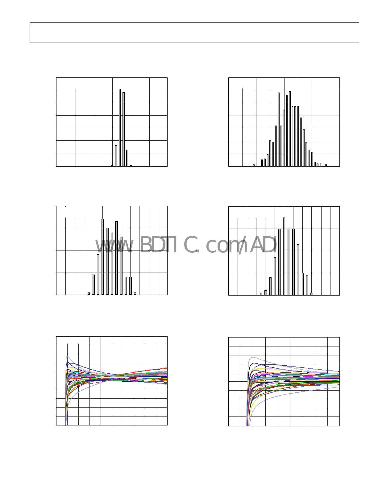
TYPICAL PERFORMANCE CHARACTERISTICS
TA = 25°C, unless otherwise noted.
280
240
VSY = ±15V
V
= 0V
CM
70
60
VSY = ±5V
V
= 0V
CM
200
160
120
80
NUMBER OF AMPLI FERS
40
0
–3 –2 –1 0 1 2 3
VOS (mV)
Figure 3. Input Offset Voltage Distribution
40
VSY = ±15V
–40°C T
30
20
NUMBER OF AMPLIFERS
10
+125°C
A
50
40
30
20
NUMBER OF AMPLI FERS
10
0
–4 –3 –2 –1 0 1 2 43
07670-003
VOS (mV)
07670-054
Figure 6. Input Offset Voltage Distribution
40
VSY = ±5V
–40°C T
30
20
NUMBER OF AMPLIFERS
10
+125°C
A
0
–20246810
TCVOS (µV/°C)
Figure 4. Input Offset Voltage Drift Distribution
5
VSY = ±15V
4
3
2
1
0
(mV)
OS
V
–1
–2
–3
–4
–5
–15 –12 –9 –6 –3 0 3 6 9 12 15
VCM (V)
Figure 5. Input Offset Voltage vs. Common-Mode Voltage
07670-005
07670-006
Rev. 0 | Page 5 of 20
0
–20246810
TCVOS (µV/°C)
Figure 7. Input Offset Voltage Drift Distribution
5
= ±5V
V
SY
4
3
2
1
0
(mV)
OS
V
–1
–2
–3
–4
–5
–4 –3 –2 –1 0 1 2 3 4 5
VCM (V)
Figure 8. Input Offset Voltage vs. Common-Mode Voltage
07670-055
07670-056
Page 6
ADA4062-2
www.BDTIC.com/ADI
10000
VSY = ±15V
10000
VSY = ±5V
1000
100
(pA)
B
I
10
1
0.1
–50 –25 0 25 50 75 100 125
TEMPERATURE (° C)
Figure 9. Input Bias Current vs. Temperature
5
VSY = ±15V
4
3
(pA)
B
I
2
1000
100
(pA)
B
I
10
1
0.1
–50 –25 0 25 50 75 100 125
07670-009
TEMPERATURE (°C)
07670-012
Figure 12. Input Bias Current vs. Temperature
3
VSY = ±5V
2
1
(pA)
B
I
0
1
0
–12–10–8–6–4 –2 0 2 4 6 810121416
VCM (V)
Figure 10. Input Bias Current vs. Input Common-Mode Voltage
10
VSY = ±15V
VCC – V
OH
1
OUTPUT VOLTAGE TO SUPPLY RAIL (V)
0.1
0.01 0.1 1 10 100
VOL – V
EE
LOAD CURRENT (mA)
Figure 11. Output Voltage to Supply Rail vs. Load Current
–1
–2
–3–2–1012345
07670-010
VCM (V)
07670-013
Figure 13. Input Bias Current vs. Input Common-Mode Voltage
10
VSY = ±5V
VCC – V
OH
1
OUTPUT VOLTAGE TO SUPPLY RAIL (V)
0.1
0.01 0.1 1 10 100
07670-011
VOL – V
EE
LOAD CURRENT (mA)
07670-014
Figure 14. Output Voltage to Supply Rail vs. Load Current
Rev. 0 | Page 6 of 20
Page 7

ADA4062-2
www.BDTIC.com/ADI
2.0
1.5
1.0
VCC – V
VOL – V
VSY = ±15V
R
= 10k
OH
EE
L
2.0
1.5
1.0
VCC – V
VOL – V
VSY = ±5V
R
OH
EE
= 10k
L
0.5
OUTPUT VOTLAGE TO SUPPLY RAIL (V)
0
–50 –25 1250 25 50 75 100
TEMPERATURE (°C)
Figure 15. Output Voltage to Supply Rail vs. Temperature
120
100
80
60
40
20
GAIN (dB)
0
–20
–40
–60
1k 10k 100k 1M 10M 100M
PHASE
GAIN
FREQUENCY (Hz)
VSY = ±15V
Figure 16. Open-Loop Gain and Phase vs. Frequency
120
100
80
60
40
20
0
–20
–40
–60
07670-015
PHASE (Degrees)
07670-016
0.5
OUTPUT VOTLAGE TO SUPPLY RAIL (V)
0
–50 –25 1250 25 50 75 100
TEMPERATURE
(°C)
Figure 18. Output Voltage to Supply Rail vs. Temperature
120
100
80
60
40
20
GAIN (dB)
0
–20
–40
–60
1k 10k 100k 1M 10M 100M
PHASE
GAIN
FREQUENCY (Hz)
Figure 19. Open-Loop Gain and Phase vs. Frequency
VSY = ±5V
120
100
80
60
40
20
0
–20
–40
–60
07670-018
PHASE (Degrees)
07670-019
50
AV = +100
40
30
AV = +10
20
10
GAIN (dB)
AV = +1
0
–10
–20
10 100 1k 10k 100k 1M 10M 100M
FREQUENCY (Hz)
VSY = ±15V
07670-017
Figure 17. Closed-Loop Gain vs. Frequency
Rev. 0 | Page 7 of 20
50
AV = +100
40
30
AV = +10
20
10
GAIN (dB)
AV = +1
0
–10
–20
10 100 1k 10k 100k 1M 10M 100M
FREQUENCY (Hz)
Figure 20. Closed-Loop Gain vs. Frequency
VSY = ±5V
07670-020
Page 8

ADA4062-2
www.BDTIC.com/ADI
1000
VSY = ±15V
100
AV = +100
()
10
AV = +10
OUT
Z
AV = +1
1
0.1
100 1k 10k 100k 1M 10M
FREQUENCY (Hz)
Figure 21. Output Impedance vs. Frequency
100
90
80
70
60
50
CMRR (dB)
40
30
20
10
0
100 1k 10k 100k 1M 10M
FREQUENCY (Hz)
VSY = ±15V
Figure 22. CMRR vs. Frequency
07670-021
07670-022
1000
VSY = ±5V
100
AV = +100
()
10
OUT
Z
AV = +10
AV = +1
1
0.1
100 1k 10k 100k 1M 10M
FREQUENCY (Hz)
Figure 24. Output Impedance vs. Frequency
100
90
80
70
60
50
CMRR (dB)
40
30
20
10
0
100 1k 10k 100k 1M 10M
FREQUENCY (Hz)
VSY = ±5V
Figure 25. CMRR vs. Frequency
07670-024
07670-025
140
120
100
80
60
PSRR (dB)
40
20
–20
0
10 100
PSRR–
1k 10k 100k 1M 10M
FREQUENCY (Hz)
VSY = ±15V
PSRR+
07670-023
Figure 23. PSRR vs. Frequency
Rev. 0 | Page 8 of 20
120
100
80
60
40
PSRR (dB)
20
–20
0
10 100
PSRR+
PSRR–
1k 10k 100k 1M 10M
FREQUENCY (Hz)
Figure 26. PSRR vs. Frequency
VSY = ±5V
07670-026
Page 9

ADA4062-2
www.BDTIC.com/ADI
60
50
VSY = ±15V
A
= +1
V
R
= 10k
L
60
50
VSY = ±5V
A
= +1
V
R
= 10k
L
40
30
OVERSHOOT (%)
20
10
0
10 100 1000 10000
CL (pF)
Figure 27. Small-Signal Overshoot vs. Load Capacitance
VSY = ±15V
V
= 20V p-p
IN
A
= +1
V
R
= 10k
L
C
= 100pF
L
VOLTAGE (5V/DIV)
40
30
OVERSHOOT (%)
20
10
0
10 100 1000 10000
07670-027
CL (pF)
07670-030
Figure 30. Small-Signal Overshoot vs. Load Capacitance
VSY = ±5V
V
= 4V p-p
IN
A
= +1
V
R
= 10k
L
C
= 100pF
L
VOLTAGE (1V/DIV )
TIME (10µs/DIV)
Figure 28. Large-Signal Transient Response
VSY = ±15V
V
= 100mV p-p
IN
A
= +1
V
R
= 10k
L
C
= 100pF
L
VOLTAGE (20mV/DIV)
TIME (10µs/DIV)
Figure 29. Small-Signal Transient Response
07670-028
TIME (4µs/DIV)
07670-031
Figure 31. Large-Signal Transient Response
VSY = ±5V
V
= 100mV p-p
IN
A
= +1
V
R
= 10k
L
C
= 100pF
L
VOLTAGE (20mV/DIV)
07670-029
TIME (10µs/DIV)
07670-032
Figure 32. Small-Signal Transient Response
Rev. 0 | Page 9 of 20
Page 10

ADA4062-2
www.BDTIC.com/ADI
4
2
0
INPUT
VSY = ±15V
4
2
0
INPUT
VSY = ±5V
OUTPUT
INPUT VOLTAGE (V)
TIME (2µs/DIV)
Figure 33. Negative Overload Recovery
2
0
–2
INPUT VOLTAGE (V)
INPUT
OUTPUT
VSY = ±15V
0
–5
–10
–15
–20
15
10
5
0
OUTPUT
OUTPUT VOL TAGE (V)
07670-033
INPUT VOLTAGE (V)
TIME (2µs/DIV)
0
OUTPUT VOLTAGE (V)
–2
–4
–6
07670-036
Figure 36. Negative Overload Recovery
2
0
–2
OUTPUT VOLTAGE (V)
INPUT VOLTAGE (V)
INPUT
OUTPUT
VSY = ±5V
4
2
OUTPUT VOLTAGE (V)
0
TIME (2µs/DIV)
Figure 34. Positive Overload Recovery
INPUT
ERROR
VOLTAGE (5V/ DIV)
BAND
OUTPUT
TIME (1µs/DIV)
VSY = ±15V
Figure 35. Positive Settling Time to 0.01%
–5
IDEAL STEP
FUNCTION
OF 10V
+10mV
0V
–10
mV
07670-042
07670-034
TIME (2µs/DIV)
Figure 37. Positive Overload Recovery
INPUT
OUTPUT
VOLTAGE (1V/DIV)
ERROR BAND
TIME (2µs/DIV)
VSY = ±5V
Figure 38. Positive Settling Time to 0.01%
–2
+2mV
0V
–2mV
07670-037
07670-035
Rev. 0 | Page 10 of 20
Page 11

ADA4062-2
www.BDTIC.com/ADI
VSY = ±15V
VSY = ±5V
VOLTAGE (5V/ DIV)
1000
100
INPUT
ERROR
BAND
TIME (1µs/DIV)
Figure 39. Negative Settling Time to 0.01%
VSY = ±15V
OUTPUT
+10mV
0V
–10mV
INPUT
ERROR BAND
VOLTAGE (1V/DIV)
07670-038
TIME (2µs/DIV)
OUTPUT
+2mV
0V
–2mV
07670-039
Figure 42. Negative Settling Time to 0.01%
1000
VSY = ±5V
100
VOLTAGE NOISE DENSI TY (nV/ Hz)
10
1 10 100 1k 10k 100k
FREQUENCY (Hz)
Figure 40. Voltage Noise Density
VSY = ±15V
INPUT NOISE VOLTAGE (0.5µV/DIV)
TIME (1s/ DIV)
Figure 41. 0.1 Hz to 10 Hz Noise
VOLTAGE NOISE DENSITY (nV/Hz)
10
1 10 100 1k 10k 100k
07670-040
FREQUENCY (Hz)
07670-043
Figure 43. Voltage Noise Density
VSY = ±5V
INPUT NOISE VOLTAGE (0.5µV/DIV)
07670-041
TIME (1s/ DIV)
07670-044
Figure 44. 0.1 Hz to 10 Hz Noise
Rev. 0 | Page 11 of 20
Page 12

ADA4062-2
www.BDTIC.com/ADI
410
410
390
370
350
330
SUPPLY CURRENT ( µA)
310
290
34567891011121314151617181920
SUPPLY VOLTAGE (±V)
125°C
85°C
25°C
–40°C
Figure 45. Supply Current vs. Supply Voltage
0
VSY = ±15V
V
= 10V p-p
IN
–20
R
= 10k
L
–40
–60
–80
390
370
350
330
310
SUPPLY CURRENT ( µA)
290
270
–50 –25 0 25 50 75 100 125
07670-045
TEMPERATURE (° C)
VSY = ±15V
VSY = ±5V
07670-048
Figure 48. Supply Current vs. Temperature
0
VSY = ±5V
V
= 5V p-p
IN
R
= 10k
–20
L
–40
–60
–80
–100
–120
CHANNEL SEPARATION (dB)
–140
–160
100 1k 10k 100k
FREQUENCY (Hz)
Figure 46. Channel Separation vs. Frequency
100
VSY = ±15V
f = 1kHz
R
= 10k
L
10
1
0.1
THD + N (%)
0.01
0.001
0.001 0.01 0. 1 1 10
AMPLITUDE ( V rms)
Figure 47. THD + N vs. Amplitude
–100
–120
CHANNEL SEPARATION (dB)
–140
–160
100 1k 10k 100k
07670-046
FREQUENCY (Hz)
07670-049
Figure 49. Channel Separation vs. Frequency
100
VSY = ±5V
f = 1kHz
R
= 10k
L
10
1
0.1
THD + N (%)
0.01
0.001
0.001 0.01 0.1 1 10
07670-047
AMPLITUDE (V rms)
07670-050
Figure 50. THD + N vs. Amplitude
Rev. 0 | Page 12 of 20
Page 13

ADA4062-2
www.BDTIC.com/ADI
10
1
VSY = ±15V
V
= 0.5 V rms
IN
R
= 10k
L
10
1
VSY = ±5V
V
= 0.5 V rms
IN
R
= 10k
L
0.1
0.01
THD + N (%)
0.001
0.0001
10 100 1k 10k 100k
FREQUENCY (Hz)
Figure 51. THD + N vs. Frequency
07670-051
0.1
0.01
THD + N (%)
0.001
0.0001
10 100 1k 10k 100k
FREQUENCY (Hz)
Figure 52. THD + N vs. Frequency
07670-052
Rev. 0 | Page 13 of 20
Page 14

ADA4062-2
www.BDTIC.com/ADI
APPLICATIONS INFORMATION
NOTCH FILTER
A notch filter rejects a specific interfering frequency and can
be implemented using a single op amp. Figure 53 shows a 60 Hz
notch filter that uses the twin T network with the ADA4062-2
configured as a voltage follower. The ADA4062-2 works as a buffer
that provides high input resistance and low output impedance.
The low bias current (2 pA typical) and high input resistance
(10 TΩ typical) of the ADA4062-2 enable large resistors and
small capacitors to be used.
Alternatively, different combinations of resistors and capacitors
values can be used to achieve the desired notch frequency.
However, the major drawback to this circuit topology is the
need to ensure that all the resistors and capacitors be closely
matched. If they are not closely matched, the notch frequency
offset and drift cause the circuit to attenuate at a frequency
other than the ideal notch frequency.
Therefore, to achieve the desired performance, 1% or better component tolerances are usually required. In addition, a notch filter
requires an op amp with a bandwidth of at least 100 to 200 times
the center frequency. Hence, using the ADA4062-2 with a
bandwidth of 1.4 MHz is excellent for a 60 Hz notch filter.
Figure 54 shows the gain of the notch filter with respect to
frequency. At 60 Hz, the notch filter has about 50 dB attenuation of signal.
+V
SY
R1
804k
IN
C1
3.3nF
1
f
=
O
2 R
1 C1
R1 = R2 = 2R3
C1 = C2 =
C3
2
Figure 53. Notch Filter Circuit
20
10
0
–10
–20
–30
GAIN (dB)
–40
–50
–60
–70
–80
10 100 1k
Figure 54. Notch Filter: Gain vs. Frequency
R2
804k
C3
6.6nF
R3
402k
C2
3.3nF
FREQUENCY (Hz)
1/2
ADA4062-2
–V
SY
V
O
07670-060
07670-057
Rev. 0 | Page 14 of 20
HIGH-SIDE SIGNAL CONDITIONING
There are many applications that require the sensing of signals
near the positive rail. The ADA4062-2 can be used in high-side
current sensing applications. Figure 55 shows a high-side signal
conditioning circuit using the ADA4062-2. The ADA4062-2 has
an input common-mode range that includes the positive supply
(−11.5 V ≤ V
≤ +15 V). In the circuit, the voltage drop across
CM
a low value resistor, such as the 0.1 Ω shown in Figure 55, is
amplified by a factor of 5 using the ADA4062-2.
+15V
100k
500k
Figure 55. High-Side Signal Conditioning
0.1
100k
500k
+15V
1/2
ADA4062-2
–15V
R
L
V
O
07670-058
MICROPOWER INSTRUMENTATION AMPLIFIER
The ADA4062-2 is a dual amplifier and is perfectly suited for
applications that require lower supply currents. For supply voltages
of ±15 V, the supply current per amplifier is 165 μA typical. The
ADA4062-2 also offers a typical low offset voltage drift of 4 μV/°C
and a very low bias current of 2 pA, which makes it well suited for
instrumentation amplifiers.
Figure 56 shows the classic 2-op-amp instrumentation amplifier
with four resistors using the ADA4062-2. The key to high CMRR
for this instrumentation amplifier are resistors that are well
matched to both the resistive ratio and relative drift. For true
difference amplification, matching of the resistor ratio is very
important, where R3/R4 = R1/R2. Assuming perfectly matched
resistors, the gain of the circuit is 1 + R2/R1, which is approximately 100. Tighter matching of two op amps in one package,
as is the case with the ADA4062-2, offers a significant boost in
performance over the 3-op-amp configuration. Overall, the circuit
only requires about 330 μA of supply current.
R3
10.1k
+15V
R4
1M
1/2
R1
10.1k
ADA4062-2
V1
V2
VO = 100(V2 – V1)
TYPICAL: 0.5mV < V2 – V1< 135mV
TYPICAL: –13.8V < V
USE MATCHED RESIS TORS
–15V
< +13.5V
O
Figure 56. Micropower Instrumentation Amplifier
R2
1M
+15V
1/2
ADA4062-2
–15V
V
O
07670-059
PHASE REVERSAL
Phase reversal occurs in some amplifiers when the input commonmode voltage range is exceeded. When the voltage driving the
input to these amplifiers exceeds the maximum input commonmode voltage range, the output of the amplifiers changes polarity.
Page 15

ADA4062-2
T
www.BDTIC.com/ADI
Most JFET input amplifiers have phase reversal if either input
exceeds the input common-mode range.
For the ADA4062-2, the output does not phase reverse if one or
both of the inputs exceeds the input voltage range but stays below
the positive supply rail and 0.5 V above the negative supply rail.
With a supply voltage of ±15 V, phase reversal occurs when the
input voltage is a negative signal greater than −14.5 V. This is due
to saturation of the input stage leading to forward biasing of the
gate-drain diode. Phase reversal in ADA4062-2 can be prevented
by using a Schottky diode to clamp the input terminals to each
other. In the simple buffer circuit in Figure 57, D1 protects the
op amp against phase reversal and R limits the input current
that flows into the op amp.
+V
SY
R
D1
10k
IN
Figure 57. Phase Reversal Solution Circuit
IN5711
1/2
ADA4062-2
–V
SY
V
O
07670-053
V
IN
V
OUT
AGE (5V/DIV)
VOL
TIME (40µs/DIV)
Figure 58. No Phase Reversal
VSY = ±15V
07670-038
Rev. 0 | Page 15 of 20
Page 16

ADA4062-2
www.BDTIC.com/ADI
SCHEMATIC
V
CC
OUT A/
OUT B
–IN A/
–IN B
Figure 59. Simplified Schematic
+IN A/
+IN B
V
EE
07670-062
Rev. 0 | Page 16 of 20
Page 17

ADA4062-2
www.BDTIC.com/ADI
OUTLINE DIMENSIONS
3.20
3.00
2.80
8
5
4
SEATING
PLANE
5.15
4.90
4.65
1.10 MAX
0.23
0.08
8°
0°
0.80
0.60
0.40
3.20
3.00
2.80
PIN 1
0.95
0.85
0.75
0.15
0.00
COPLANARITY
1
0.65 BSC
0.38
0.22
0.10
COMPLIANT TO JEDEC STANDARDS MO-187-AA
Figure 60. 8-Lead Mini Small Outline Package [MSOP]
(RM-8)
Dimensions shown in millimeters
5.00 (0.1968)
4.80 (0.1890)
4.00 (0.1574)
3.80 (0.1497)
0.25 (0.0098)
0.10 (0.0040)
COPLANARITY
0.10
CONTROLL ING DIMENSI ONS ARE IN MILLIMETERS; INCH DI MENSIONS
(IN PARENTHESES) ARE ROUNDED-OFF MILLIMETER EQUIVALENTS FOR
REFERENCE ONLY AND ARE NOT APPROPRI ATE FOR USE IN DESIGN.
85
1
1.27 (0.0500)
SEATING
PLANE
COMPLIANT TO JEDEC STANDARDS MS-012-A A
BSC
6.20 (0.2441)
5.80 (0.2284)
4
1.75 (0.0688)
1.35 (0.0532)
0.51 (0.0201)
0.31 (0.0122)
8°
0°
0.25 (0.0098)
0.17 (0.0067)
0.50 (0.0196)
0.25 (0.0099)
1.27 (0.0500)
0.40 (0.0157)
45°
012407-A
Figure 61. 8-Lead Standard Small Outline Package [SOIC_N]
Narrow Body
(R-8)
Dimensions shown in millimeters and (inches)
Rev. 0 | Page 17 of 20
Page 18

ADA4062-2
www.BDTIC.com/ADI
ORDERING GUIDE
Model Temperature Range Package Description Package Option Branding
ADA4062-2ARMZ
ADA4062-2ARMZ-RL
ADA4062-2ARZ
ADA4062-2ARZ-R7
ADA4062-2ARZ-RL
ADA4062-2BRZ
ADA4062-2BRZ-R7
ADA4062-2BRZ-RL
1
Z = RoHS Compliant Part.
1
−40°C to +125°C 8-Lead MSOP RM-8 A25
1
−40°C to +125°C 8-Lead MSOP RM-8 A25
1
−40°C to +125°C 8-Lead SOIC_N R-8
1
−40°C to +125°C 8-Lead SOIC_N R-8
1
−40°C to +125°C 8-Lead SOIC_N R-8
1
−40°C to +125°C 8-Lead SOIC_N R-8
1
−40°C to +125°C 8-Lead SOIC_N R-8
1
−40°C to +125°C 8-Lead SOIC_N R-8
Rev. 0 | Page 18 of 20
Page 19

ADA4062-2
www.BDTIC.com/ADI
NOTES
Rev. 0 | Page 19 of 20
Page 20

ADA4062-2
www.BDTIC.com/ADI
NOTES
©2008 Analog Devices, Inc. All rights reserved. Trademarks and
registered trademarks are the property of their respective owners.
D07670-0-10/08(0)
Rev. 0 | Page 20 of 20
 Loading...