

Page 1
10-Bit CCD Signal Processor with
FEATURES
6-Phase Vertical Transfer Clock Support
Correlated Double Sampler (CDS)
6 dB to 42 dB 10-Bit Variable Gain Amplifi er (VGA)
10- Bit 27 MHz A/D Converter
Black Level Clamp with Variable Level Control
Complete On-Chip Timing Generator
Precision Timing Core with 800 ps Resolution
On-Chip 3 V Horizontal and RG Drivers
2-Phase and 4-Phase H-Clock Modes
Electronic and Mechanical Shutter Modes
On-Chip Driver for External Crystal
On-Chip Sync Generator with External Sync Input
56-Lead LFCSP Package
APPLICATIONS
Digital Still Cameras
Digital Video Camcorders
Industrial Imaging
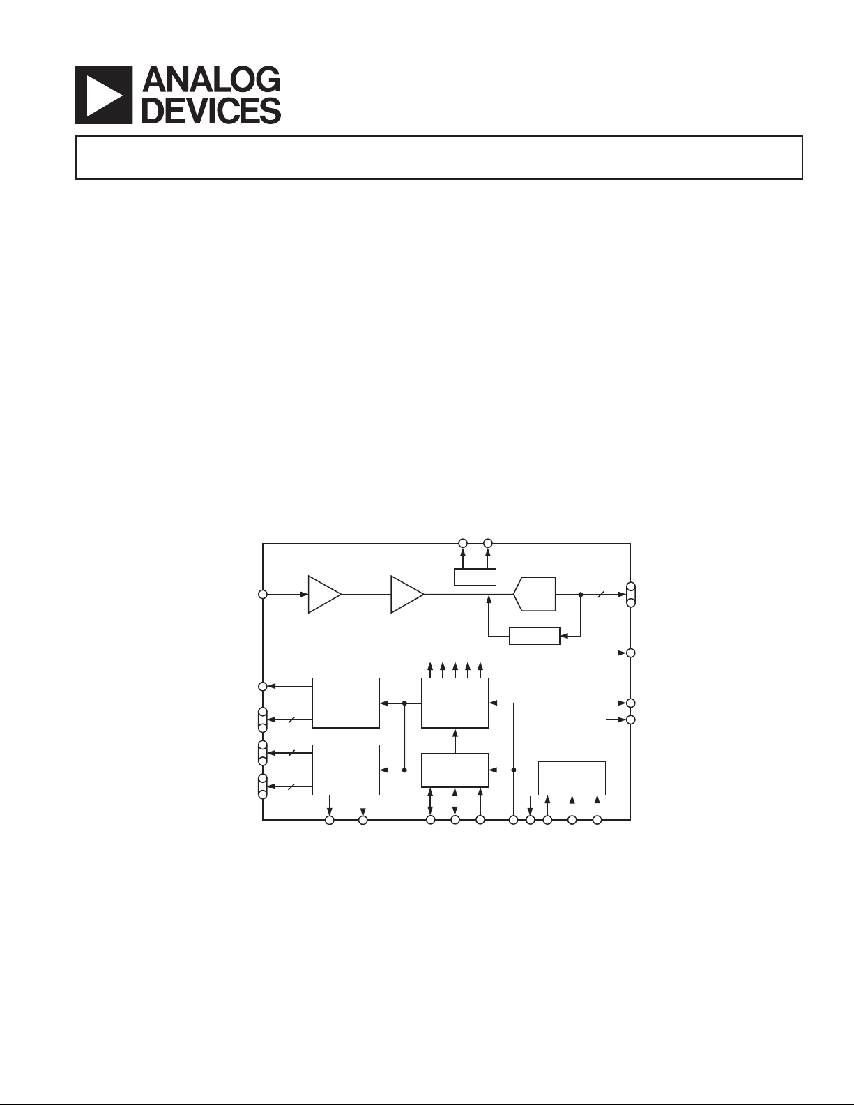
FUNCTIONAL BLOCK DIAGRAM
Precision Timing
™
Generator
AD9991
GENERAL DESCRIPTION
The AD9991 is a highly integrated CCD signal processor for
digital still camera and camcorder applications. It includes a
complete analog front end with A/D conversion, combined with a
full-function programmable timing generator. The timing generator is capable of supporting both 4- and 6-phase vertical clocking.
A Precision Timing core allows adjustment of high speed clocks
with 800 ps resolution at 27 MHz operation.
The AD9991 is specifi ed at pixel rates of up to 27 MHz. The
analog front end includes black level clamping, CDS, VGA,
and a 10-bit A/D converter. The timing generator provides all
the necessary CCD clocks: RG, H-clocks, V-clocks, sensor gate
pulses, substrate clock, and substrate bias control. Operation is
programmed using a 3-wire serial interface.
Packaged in a space-saving 56-lead LFCSP, the AD9991 is specifi ed over an operating temperature range of –20°C to +85°C.
VRT VRB
REV. 0
CCDIN
H1–H4
V1–V6
VSG1–VSG5
RG
6dB TO 42dB
CDS
HORIZONTAL
DRIVERS
4
6
V- H
CONTROL
5
VSUB SUBCK HD VD SYNC
VGA
INTERNAL CLOCKS
VREF
PRECISION
TIMING
GENERATOR
SYNC
GENERATOR
10-BIT
ADC
CLAMP
CLOCLI
AD9991
INTERNAL
REGISTERS
SL SCK DATA
10
DOUT
DCLK
MSHUT
STROBE
Information furnished by Analog Devices is be lieved to be accurate and
reliable. However, no responsibility is assumed by Analog Devices for its
use, nor for any infringements of patents or other rights of third parties
that may result from its use. No license is granted by implication or otherwise under any patent or patent rights of Analog Devices. Trademarks
and registered trademarks are the property of their respective companies.
One Technology Way, P.O. Box 9106, Norwood, MA 02062-9106, U.S.A.
Tel: 781/329-4700 www.analog.com
Fax: 781/326-8703 © 2003 Analog Devices, Inc. All rights reserved.
Page 2

AD9991
TABLE OF CONTENTS
SPECIFICATIONS ............................................................... 3
Digital Specifi cations .......................................................... 3
Analog Specifi cations ...........................................................4
Timing Specifi cations ........................................................... 5
ABSOLUTE MAXIMUM RATINGS .....................................5
PACKAGE THERMAL CHARACTERISTICS ...................... 5
ORDERING GUIDE .............................................................5
PIN CONFIGURATION .......................................................6
PIN FUNCTION DESCRIPTIONS....................................... 6
TERMINOLOGY ..................................................................7
EQUIVALENT CIRCUITS .................................................... 7
TYPICAL PERFORMANCE CHARACTERISTICS .............8
SYSTEM OVERVIEW............................................................ 9
PRECISION TIMING HIGH SPEED TIMING
GENERATION .................................................................... 10
Timing Resolution .............................................................10
High Speed Clock Programmability.................................... 10
H-Driver and RG Outputs ................................................. 11
Digital Data Outputs ........................................................ 11
HORIZONTAL CLAMPING AND BLANKING ................. 13
Individual CLPOB and PBLK Patterns ..............................13
Individual HBLK Patterns .................................................13
Generating Special HBLK Patterns .................................... 14
Generating HBLK Line Alteration ..................................... 14
HORIZONTAL TIMING SEQUENCE EXAMPLE .............15
VERTICAL TIMING GENERATION ................................. 16
Ver tical Pattern Groups ...................................................... 17
Ver tical Sequences..............................................................18
Complete Field: Combining V-Sequences ........................... 19
Generating Line Alternation for V-Sequence and HBLK...... 20
Second V-Pattern Group during VSG Active Line................ 20
Sweep Mode Operation...................................................... 21
Multiplier Mode ................................................................ 21
Ver tical Sensor Gate (Shift Gate) Patterns........................... 22
MODE Register ................................................................ 23
VERTICAL TIMING EXAMPLE ....................................... 24
Important Note about Signal Polarities ............................... 24
SHUTTER TIMING CONTROL ........................................ 26
Normal Shutter Operation ................................................. 26
High Precision Shutter Operation.......................................26
Low Speed Shutter Operation ............................................ 26
SUBCK Suppression ......................................................... 27
Readout after Exposure...................................................... 27
Using the TRIGGER Register ............................................27
VSUB Control ................................................................... 28
MSHUT and STROBE Control ........................................ 28
TRIGGER Register Limitations ......................................... 29
EXPOSURE AND READOUT EXAMPLE.......................... 30
ANALOG FRONT END DESCRIPTION
AND OPERATION ......................................................... 31
DC Restore ..................................................................... 31
Correlated Double Sampler............................................... 31
Variable Gain Amplifi er .................................................... 31
A/D Converter .................................................................. 31
Optical Black Clamp......................................................... 32
Digital Data Outputs ......................................................... 32
POWER-UP AND SYNCHRONIZATION ........................... 33
Recommended Power-Up Sequence for Master Mode......... 33
Generating Software SYNC without
External SYNC Signal ................................................... 33
SYNC during Master Mode Operation...............................34
Power-Up and Synchronization in Slave Mode.................... 34
STANDBY MODE OPERATION ........................................34
CIRCUIT LAYOUT INFORMATION ................................. 36
SERIAL INTERFACE TIMING........................................... 37
Register Address Banks 1 and 2..........................................38
Updating of New Register Values........................................ 39
COMPLETE LISTING OF REGISTER BANK 1 ............... 40
COMPLETE LISTING OF REGISTER BANK 2 ............... 43
OUTLINE DIMENSIONS.................................................. 59
–2–
REV. 0
Page 3
AD9991–SPECIFICATIONS
Parameter Min Typ Max Unit
TEMPERATURE RANGE
Operating –20 +85 °C
Storage –65 +150 °C
POWER SUPPLY VOLTAGE
AVDD (AFE Analog Supply) 2.7 3.0 3.6 V
TCVDD (Timing Core Analog Supply) 2.7 3.0 3.6 V
RGVDD (RG Driver) 2.7 3.0 3.6 V
HVDD (H1–H4 Drivers) 2.7 3.0 3.6 V
DRVDD (Data Output Drivers) 2.7 3.0 3.6 V
DVDD (Digital) 2.7 3.0 3.6 V
POWER DISSIPATION (See TPC 1 for Power Curves)
27 MHz, Typ Supply Levels, 100 pF H1–H4 Loading 270 mW
Power from HVDD Only* 100 mW
Standby 1 Mode 105 mW
Standby 2 Mode 10 mW
Standby 3 Mode 0.5 mW
MAXIMUM CLOCK RATE (CLI) 27 MHz
*The total power dissipated by the HVDD supply may be approximated using the equation
To tal HVDD Power = [C
Reducing the H-loading, using only two of the outputs, and/or using a lower HVDD supply will reduce the power dissipation.
Specifi cations subject to change without notice.
HVDD Pixel Frequency] HVDD Number of H-outputs used
LOAD
DIGITAL SPECIFICATIONS
(RGVDD = HVDD = DVDD = DRVDD = 2.7 V to 3.6 V, CL = 20 pF, T
MIN
to T
, un less oth er wise noted.)
MAX
Parameter Symbol Min Typ Max Unit
LOGIC INPUTS
High Level Input Voltage V
Low Level Input Voltage V
High Level Input Current I
Low Level Input Current I
Input Capacitance C
2.1 V
IH
0.6 V
IL
10 µA
IH
10 µA
IL
10 pF
IN
LOGIC OUTPUTS (Except H and RG)
High Level Output Voltage @ I
Low Level Output Voltage @ I
= 2 mA VOH 2.2 V
OH
= 2 mA VOL 0.5 V
OL
RG and H-DRIVER OUTPUTS (H1–H4)
High Level Output Voltage @ Max Current V
Low Level Output Voltage @ Max Current V
VDD – 0.5 V
OH
0.5 V
OL
Maximum Output Current (Programmable) 30 mA
Maximum Load Capacitance (For Each Output) 100 pF
Specifi cations subject to change without notice.
REV. 0
–3–
Page 4
AD9991
ANALOG SPECIFICATIONS
(AVDD = 3.0 V, f
= 27 MHz, Typical Timing Specifi cations, T
CLI
MIN
to T
, unless otherwise noted.)
MAX
Parameter Min Typ Max Unit Notes
CDS*
Allowable CCD Reset Transient 500 mV
Max Input Range before Saturation 1.0 V p-p
Max CCD Black Pixel Amplitude ±50 mV
VARIABLE GAIN AMPLIFIER (VGA)
Gain Control Resolution 1024 Steps
Gain Monotonicity Guaranteed
Gain Range
Min Gain (VGA Code 0) 6 dB
Max Gain (VGA Code 1023) 42 dB
BLACK LEVEL CLAMP
Clamp Level Resolution 256 Steps
Clamp Level Measured at ADC output.
Min Clamp Level (Code 0) 0 LSB
Max Clamp Level (Code 255) 63.75 LSB
A/D CONVERTER
Resolution 10 Bits
Differential Nonlinearity (DNL) –1.0 ±0.5 +1.0 LSB
No Missing Codes Guaranteed
Full-Scale Input Voltage 2.0 V
VOLTAGE REFERENCE
Reference Top Voltage (REFT) 2.0 V
Reference Bottom Voltage (REFB) 1.0 V
SYSTEM PERFORMANCE Includes entire signal chain.
Gain Accuracy
Low Gain (VGA Code 0) 5.0 5.5 6.0 dB Gain = (0.0351 Code) + 6 dB
Max Gain (VGA Code 1023) 40.5 41.5 42.5 dB
Peak Nonlinearity, 500 mV Input Signal 0.2 % 12 dB gain applied.
Total Output Noise 0.25 LSB rms AC grounded input, 6 dB gain applied.
Power Supply Rejection (PSR) 50 dB Measured with step change on supply.
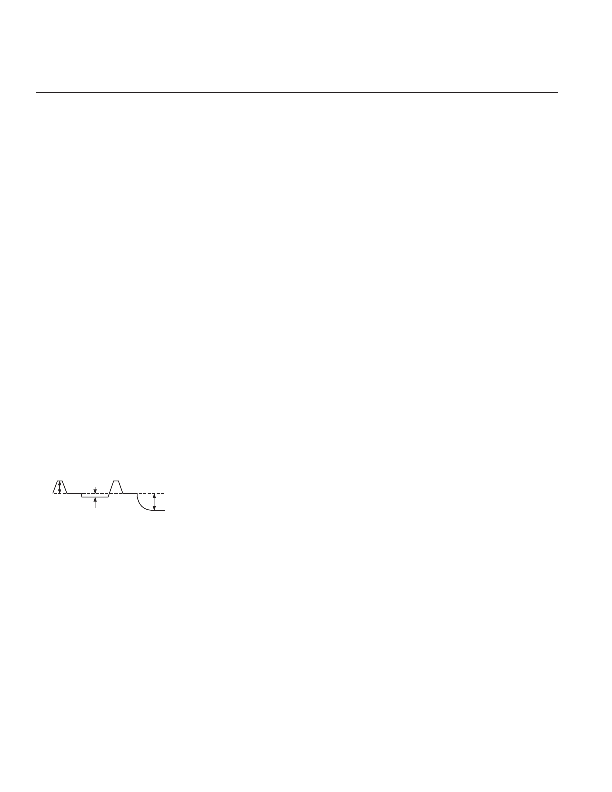
*Input signal characteristics defi ned as follows:
500mV TYP
RESET TRANSIENT
Specifi cations subject to change without notice.
50mV MAX
OPTICAL BLACK PIXEL
1V MAX
INPUT SIGNAL RANGE
–4–
REV. 0
Page 5
AD9991
TIMING SPECIFICATIONS
(CL = 20 pF, AVDD = DVDD = DRVDD = 3.0 V, f
= 27 MHz, unless otherwise noted.)
CLI
Parameter Symbol Min Typ Max Unit
MASTER CLOCK, CLI (Figure 4)
CLI Clock Period t
CONV
37 ns
CLI High/Low Pulsewidth 14.8 18.5 21.8 ns
Delay from CLI Rising Edge to Internal Pixel Position 0 t
AFE CLPOB Pulsewidth
AFE SAMPLE LOCATION
1, 2
(Figures 9 and 14) 2 20 Pixels
1
(Figure 7)
SHP Sample Edge to SHD Sample Edge t
DATA OUTPUTS (Figures 8a and 8b)
Output Delay from DCLK Rising Edge
1
tOD 8 ns
CLIDLY
S1
17 18.5 ns
6 ns
Pipeline Delay from SHP/SHD Sampling to DOUT 11 Cycles
SERIAL INTERFACE (Figures 40a and 40b)
Maximum SCK Frequency f
SL to SCK Setup Time t
SCK to SL Hold Time t
SDATA Valid to SCK Rising Edge Setup t
SCK Falling Edge to SDATA Valid Hold t
SCK Falling Edge to SDATA Valid Read t
NOTES
1
Parameter is programmable.
2
Minimum CLPOB pulsewidth is for functional operation only. Wider typical pulses are recommended to achieve good clamp performance.
Specifi cations subject to change without notice.
ABSOLUTE MAXIMUM RATINGS*
With
Respect
Parameter To Min Max Unit
10 MHz
SCLK
10 ns
LS
10 ns
LH
DS
10 ns
DH
10 ns
DV
10 ns
PA CKAGE THERMAL CHARACTERISTICS
Thermal Resistance
JA = 25°C/W*
*
is measured using a 4-layer PCB with the exposed paddle soldered to the
JA
board.
AVDD AVSS –0.3 +3.9 V
TCVDD TCVSS –0.3 +3.9 V
HVDD HVSS –0.3 +3.9 V
RGVDD RGVSS –0.3 +3.9 V
DVDD DVSS –0.3 +3.9 V
DRVDD DRVSS –0.3 +3.9 V
RG Output RGVSS –0.3 RGVDD + 0.3 V
Temperature Package Package
Model Range Description Option
AD9991KCP –20°C to +85°C LFCSP CP-56
AD9991KCPRL –20°C to +85°C LFCSP CP-56
ORDERING GUIDE
H1–H4 Output HVSS –0.3 HVDD + 0.3 V
Digital Outputs DVSS –0.3 DVDD + 0.3 V
Digital Inputs DVSS –0.3 DVDD + 0.3 V
SCK, SL, SDATA DVSS –0.3 DVDD + 0.3 V
REFT, REFB, CCDIN AVSS –0.3 AVDD + 0.3 V
Junction Temperature 150 °C
Lead Temperature, 10 sec 350 °C
*Stresses above those listed under Absolute Maximum Ratings may cause permanent
damage to the device. This is a stress rating only. Functional operation of the device
at these or any other conditions above those listed in the operational sections of
this specifi cation is not implied. Exposure to absolute maximum rating conditions
for extended periods may affect device reliability. Absolute maximum ratings apply
individually only, not in combination. Unless otherwise specifi ed, all other voltages
are referenced to GND.
CAUTION
ESD (electrostatic discharge) sensitive device. Electrostatic charges as high as 4000 V readily ac cu mu late on
the human body and test equipment and can discharge without detection. Although the AD9991 features
proprietary ESD pro tec tion circuitry, permanent damage may occur on devices subjected to high energy
electrostatic discharges. Therefore, proper ESD pre cau tions are rec om mend ed to avoid per for mance
deg ra da tion or loss of functionality.
REV. 0
–5–
Page 6
AD9991
PIN CONFIGURATION
48 DVSS
52 NC
51 DCLK
49 DVDD
50 HD
55 D1
56 D2
54 D0
53 NC
47 VD
46 SYNC
44 MSHUT
43 SCK
45 STROBE
D3 1
D4 2
D5 3
D6 4
D7 5
D8 6
D9 7
DRVDD 8
DRVSS 9
VSUB 10
SUBCK 11
V1 12
V2 13
V3 14
PIN 1
IDENTIFIER
V4 15
V5 16
V6 17
VSG1 18
AD9991
TOP VIEW
VSG2 19
VSG3 20
PIN FUNCTION DESCRIPTIONS
Pin Mnemonic Type2 Description
1 D3 DO Data Output
2 D4 DO Data Output
3 D5 DO Data Output
4 D6 DO Data Output
5 D7 DO Data Output
6 D8 DO Data Output
7 D9 DO Data Output (MSB)
8 DRVDD P Data Output Driver Supply
9 DRVSS P Data Output Driver Ground
10 VSUB DO CCD Substrate Bias
11 SUBCK DO CCD Substrate Clock (E-Shutter)
12 V1 DO CCD Vertical Transfer Clock 1
13 V2 DO CCD Vertical Transfer Clock 2
14 V3 DO CCD Vertical Transfer Clock 3
15 V4 DO CCD Vertical Transfer Clock 4
16 V5 DO CCD Vertical Transfer Clock 5
17 V6 DO CCD Vertical Transfer Clock 6
18 VSG1 DO CCD Sensor Gate Pulse 1
19 VSG2 DO CCD Sensor Gate Pulse 2
20 VSG3 DO CCD Sensor Gate Pulse 3
21 VSG4 DO CCD Sensor Gate Pulse 4
22 VSG5 DO CCD Sensor Gate Pulse 5
23 H1 DO CCD Horizontal Clock 1
24 H2 DO CCD Horizontal Clock 2
25 HVSS P H1–H4 Driver Ground
26 HVDD P H1–H4 Driver Supply
27 H3 DO CCD Horizontal Clock 3
28 H4 DO CCD Horizontal Clock 4
29 RGVSS P RG Driver Ground
30 RG DO CCD Reset Gate Clock
31 RGVDD P RG Driver Supply
32 TCVSS P Analog Ground for Timing Core
33 TCVDD P Analog Supply for Timing Core
34 CLO DO Clock Output for Crystal
35 CLI DI Reference Clock Input
42 SDI
41 SL
40 REFB
39 REFT
38 AVSS
37 CCDIN
36 AVDD
35 CLI
34 CLO
33 TCVDD
32 TCVSS
31 RGVDD
30 RG
29 RGVSS
H1 23
VSG4 21
VSG5 22
H2 24
HVSS 25
H3 27
H4 28
HVDD 26
1
Pin Mnemonic Type2 Description
36 AVDD P Analog Supply for AFE
37 CCDIN AI CCD Signal Input
38 AVSS P Analog Ground for AFE
39 REFT AO Voltage Reference Top Bypass
40 REFB AO Voltage Reference Bottom Bypass
41 SL DI 3-Wire Serial Load Pulse
42 SDI DI 3-Wire Serial Data Input
43 SCK DI 3-Wire Serial Clock
44 MSHUT DO Mechanical Shutter Pulse
45 STROBE DO Strobe Pulse
46 SYNC DI External System Sync Input
47 VD DIO Vertical Sync Pulse
(Input for Slave Mode,
Output for Master Mode)
48 DVSS P Digital Ground
49 DVDD P Power Supply for VSG, V1–V6,
HD/VD, MSHUT, STROBE,
SYNC, and Serial Interface
50 HD DIO Horizontal Sync Pulse
(Input for Slave Mode, Output for
Master Mode)
51 DCLK DO Data Clock Output
52 NC Not Internally Connected
53 NC Not Internally Connected
54 D0 DO Data Output (LSB)
55 D1 DO Data Output
56 D2 DO Data Output
NOTES
1
See Figure 38 for circuit confi guration.
2
AI = Analog Input, AO = Analog Output, DI = Digital Input,
DO = Digital Output, DIO = Digital Input/Output, P = Power.
–6–
REV. 0
Page 7
AD9991
T
TERMINOLOGY
Differential Nonlinearity (DNL)
An ideal ADC exhibits code transitions that are exactly 1 LSB
apart. DNL is the deviation from this ideal value. Thus every
code must have a fi nite width. No missing codes guaranteed to
10-bit resolution indicates that all 1024 codes must be present
over all operating conditions.
Peak Nonlinearity
Peak nonlinearity, a full signal chain specifi cation, refers to
the peak deviation of the output of the AD9991 from a true
straight line. The point used as zero scale occurs 0.5 LSB
before the fi rst code transition. Positive full scale is defi ned as
a level 1.5 LSB beyond the last code transition. The deviation
is measured from the middle of each particular output code to
the true straight line. The error is then expressed as a percent-
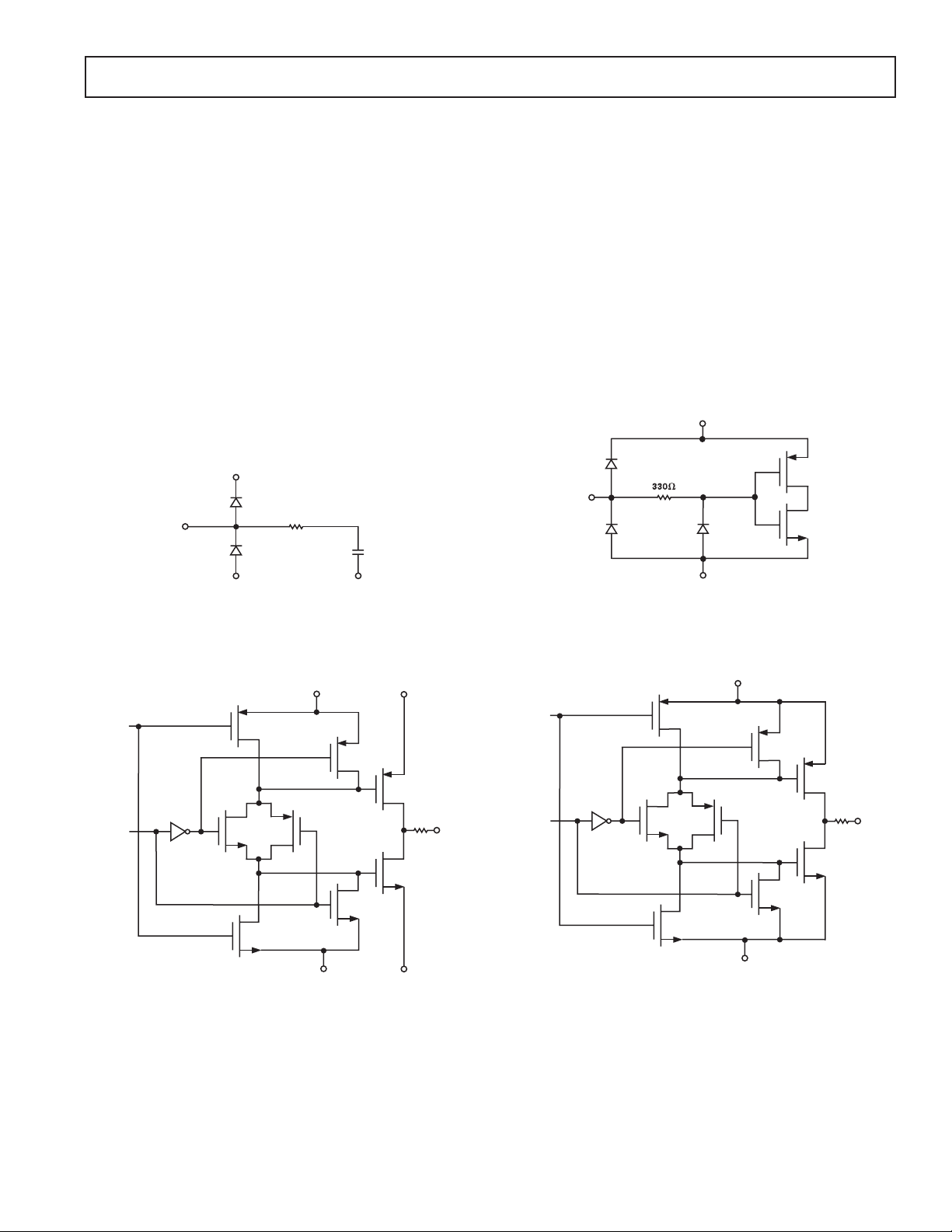
EQUIVALENT CIRCUITS
AV DD
R
age of the 2 V ADC full-scale signal. The input signal is always
appropriately gained up to fi ll the ADC’s full-scale range.
Total Output Noise
The rms output noise is measured using histogram techniques.
The standard deviation of the ADC output codes is calculated in
LSB and represents the rms noise level of the total signal chain at
the specifi ed gain setting. The output noise can be converted to
an equivalent voltage using the relationship 1 LSB = (ADC Full
n
Scale/2
codes), where n is the bit resolution of the ADC. For the
AD9991, 1 LSB is 1.95 mV.
Power Supply Rejection (PSR)
The PSR is measured with a step change applied to the supply
pins. The PSR specifi cation is calculated from the change in the
data outputs for a given step change in the supply voltage.
DVD D
DATA
THREE-
STATE
AVSS AVSS
Circuit 1. CCDIN
DVD D
DVSS
Circuit 2. Digital Data Outputs
DRVDD
DRVSS
DOUT
RG, H1–H4
ENABLE
DVSS
Circuit 3. Digital Inputs
HVDD OR
RGVDD
HVSS OR
RGVSS
Circuit 4. H1–H4, RG Drivers
OUTPU
REV. 0
–7–
Page 8
AD9991–Typical Performance Characteristics
350
TOTA L H1-4 LOAD = 400 pF
300
250
200
POWER DISSIPATION (mW)
150
100
10
VDD = 3.3V
15
SAMPLE RATE (MHz)
VDD = 3.0V
21
TPC 1. Power Dissipation vs. Sample Rate
1.0
0.5
VDD = 2.7V
10
7.5
5
OUTPUT NOISE (LSB)
2.5
27
0
0
200
400
VGA GAIN CODE (LSB)
600 800
1000
TPC 3. Output Noise vs. VGA Gain
0
DNL (LSB)
–0.5
–1.0
0
200 600 800
400
CODES
TPC 2. Typical DNL Performance
1000
–8–
REV. 0
Page 9
AD9991
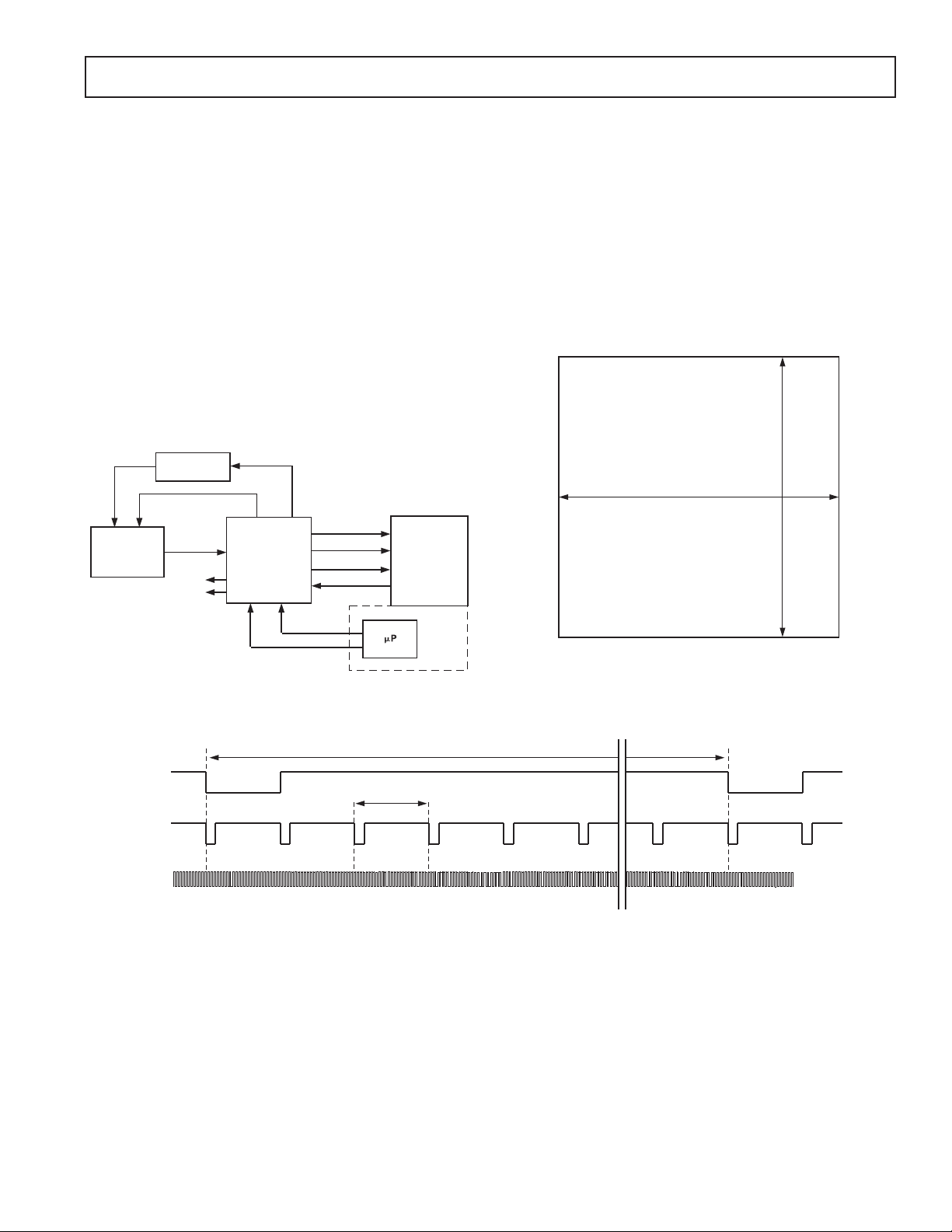
SYSTEM OVERVIEW
Figure 1 shows the typical system block diagram for the AD9991
used in Master mode. The CCD output is processed by the
AD9991’s AFE circuitry, which consists of a CDS, VGA, black
level clamp, and A/D converter. The digitized pixel information
is sent to the digital image processor chip, which performs the
postprocessing and compression. To operate the CCD, all CCD
timing parameters are programmed into the AD9991 from the
system microprocessor through the 3-wire serial interface. From
the system master clock, CLI, provided by the image processor
or external crystal, the AD9991 generates all of the CCD’s horizontal and vertical clocks and all internal AFE clocks. External
synchronization is provided by a SYNC pulse from the microprocessor, which will reset internal counters and resync the VD and
HD outputs.
Alternatively, the AD9991 may be operated in Slave mode, in
which VD and HD are provided externally from the image processor. In this mode, all AD9991 timing will be synchronized
with VD and HD.
V1–V6, VSG1–VSG5, SUBCK
AD9991
AFETG
SYNC
SERIAL
INTERFACE
DOUT
DCLK
HD, VD
CLI
DIGITAL
IMAGE
PROCESSING
ASIC
CCD
V- DRIVER
H1–H4, RG, VSUB
CCDIN
MSHUT
STROBE
The H-drivers for H1–H4 and RG are included in the AD9991,
allowing these clocks to be directly connected to the CCD.
H-drive voltage of up to 3.3 V is supported. An external V-driver
is required for the vertical transfer clocks, the sensor gate pulses,
and the substrate clock.
The AD9991 also includes programmable MSHUT and
STROBE outputs, which may be used to trigger mechanical
shutter and strobe (fl ash) circuitry.
Figures 2 and 3 show the maximum horizontal and vertical
counter dimensions for the AD9991. All internal horizontal and
vertical clocking is controlled by these counters to specify line
and pixel locations. Maximum HD length is 4095 pixels per line,
and maximum VD length is 4095 lines per fi eld.
MAXIMUM
FIELD
DIMENSIONS
12-BIT HORIZONTAL = 4096 PIXELS MAX
12-BIT VERTICAL = 4096 LINES MAX
Figure 1. Typical System Block Diagram, Master Mode
MAX VD LENGTH IS 4095 LINES
VD
HD
CLI
MAX HD LENGTH IS 4095 PIXELS
Figure 3. Maximum VD/HD Dimensions
Figure 2. Vertical and Horizontal Counters
REV. 0
–9–
Page 10
AD9991
PRECISION TIMING HIGH SPEED TIMING GENERATION
The AD9991 generates high speed timing signals using the
fl exible Precision Timing core. This core is the foundation for
generating the timing used for both the CCD and the AFE: the
reset gate RG, horizontal drivers H1–H4, and the SHP/SHD
sample clocks. A unique architecture makes it routine for the
system designer to optimize image quality by providing precise
control over the horizontal CCD readout and the AFE correlated
double sampling.
The high speed timing of the AD9991 operates the same in either
Master or Slave mode confi guration. For more information on
synchronization and pipeline delays, see the Power-Up and Synchronization section.
Timing Resolution
The Precision Timing core uses a 1 master clock input (CLI)
as a reference. This clock should be the same as the CCD pixel
clock frequency. Figure 4 illustrates how the internal timing core
divides the master clock period into 48 steps or edge positions.
Using a 20 MHz CLI frequency, the edge resolution of the Precision Timing core is 1 ns. If a 1 system clock is not available, it
is also possible to use a 2 reference clock by programming the
POSITION
CLI
P[0] P[48] = P[0]P[12] P[24] P[36]
CLIDIVIDE register (Addr 0x30). The AD9991 will then internally divide the CLI frequency by 2.
The AD9991 also includes a master clock output, CLO, which is
the inverse of CLI. This output is intended to be used as a crystal
driver. A crystal can be placed between the CLI and CLO pins to
generate the master clock for the AD9991. For more information
on using a crystal, see Figure 39.
High Speed Clock Programmability
Figure 5 shows how the high speed clocks RG, H1–H4, SHP, and
SHD are generated. The RG pulse has programmable rising and
falling edges, and may be inverted using the polarity control. The
horizontal clocks H1 and H3 have programmable rising and falling edges and polarity control. The H2 and H4 clocks are always
inverses of H1 and H3, respectively. Table I summarizes the high
speed timing registers and their parameters. Figure 6 shows the
typical 2-phase H-clock arrangement in which H3 and H4 are
programmed for the same edge location as H1 and H2.
The edge location registers are six bits wide, but there are only
48 valid edge locations available. Therefore, the register values
aremapped into four quadrants, with each quadrant containing
t
CLIDLY
1 PIXEL
PERIOD
NOTES
PIXEL CLOCK PERIOD IS DIVIDED INTO 48 POSITIONS, PROVIDING FINE EDGE RESOLUTION FOR HIGH SPEED CLOCKS.
THERE IS A FIXED DELAY FROM THE CLI INPUT TO THE INTERNAL PIXEL PERIOD POSITIONS (
t
CLIDLY
= 6ns TYP).
Figure 4. High Speed Clock Resolution from CLI Master Clock Input
3
CCD
SIGNAL
12
RG
56
H1
H2
78
H3
4
H4
PROGRAMMABLE CLOCK POSITIONS:
1. RG RISING EDGE
2. RG FALLING EDGE
3. SHP SAMPLE LOCATION
4. SHD SAMPLE LOCATION
Figure 5. High Speed Clock Programmable Locations
5. H1 RISING EDGE POSITION
6. H1 FALLING EDGE POSITION (H2 IS INVERSE OF H1)
7. H3 RISING EDGE POSITION
8. H3 FALLING EDGE POSITION (H4 IS INVERSE OF H3)
–10–
REV. 0
Page 11
AD9991
12 edge locations. Table II shows the correct register values for
the corresponding edge locations.
Figure 7 shows the default timing locations for all of the high
speed clock signals.
H-Driver and RG Outputs
In addition to the programmable timing positions, the AD9991
features on-chip output drivers for the RG and H1–H4 outputs.
These drivers are powerful enough to directly drive the CCD
inputs. The H-driver and RG current can be adjusted for optimum
rise/fall time into a particular load by using the DRVCONTROL
register (Addr 0x35). The 3-bit drive setting for each output is
adjustable in 4.1 mA increments, with the minimum setting of 0
equal to OFF or three-state, and the maximum setting of 7 equal
to 30.1 mA.
As shown in Figures 5, 6, and 7, the H2 and H4 outputs are
inverses of H1 and H3, respectively. The H1/H2 crossover voltage is approximately 50% of the output swing. The crossover
voltage is not programmable.
Ta b le I. Timing Core Register Parameters for H1, H3, RG, SHP/SHD
Digital Data Outputs
The AD9991 data output and DCLK phases are programmable
using the DOUTPHASE register (Addr 0x37, Bits [5:0]). Any
edge from 0 to 47 may be programmed, as shown in Figure 8a.
Normally, the DOUT and DCLK signals will track in phase based
on the DOUTPHASE register contents. The DCLK output phase
can also be held fi xed with respect to the data outputs by changing the DCLKMODE register HIGH (Addr 0x37, Bit 6). In this
mode, the DCLK output will remain at a fi xed phase equal to
CLO (the inverse of CLI) while the data output phase is still
programmable.
There is a fi xed output delay from the DCLK rising edge to the
DOUT transition, called t
. This delay can be programmed to
OD
four values between 0 ns and 12 ns, by using the DOUTDELAY
register (Addr 0x037, Bits [8:7]). The default value is 8 ns.
The pipeline delay through the AD9991 is shown in Figure 8b.
After the CCD input is sampled by SHD, there is an 11-cycle
delay until the data is available.
Parameter Length Range Description
Polarity 1b High/Low Polarity Control for H1, H3, and RG (0 = No Inversion, 1 = Inversion)
Positive Edge 6b 0–47 Edge Location Positive Edge Location for H1, H3, and RG
Negative Edge 6b 0–47 Edge Location Negative Edge Location for H1, H3, and RG
Sampling Location 6b 0-47 Edge Location Sampling Location for Internal SHP and SHD Signals
Drive Strength 3b 0–47 Current Steps Drive Current for H1–H4 and RG Outputs (4.1 mA per Step)
CCD
SIGNAL
RG
H1/H3
H2/H4
USING THE SAME TOGGLE POSITIONS FOR H1 AND H3 GENERATES STANDARD 2-PHASE H-CLOCKING.
Figure 6. 2-Phase H-Clock Operation
Ta b le II. Precision Timing Edge Locations
Quadrant Edge Location (Dec) Register Value (Dec) Register Value (Bin)
I 0 to 11 0 to 11 000000 to 001011
II 12 to 23 16 to 27 010000 to 011011
III 24 to 35 32 to 43 100000 to 101011
IV 36 to 47 48 to 59 110000 to 111011
REV. 0
–11–
Page 12
AD9991
POSITION
PIXEL
PERIOD
RG
H1/H3
H2/H4
CCD
SIGNAL
P[0]
RGr[0]
Hr[0]
NOTES
ALL SIGNAL EDGES ARE FULLY PROGRAMMABLE TO ANY OF THE 48 POSITIONS WITHIN ONE PIXEL PERIOD.
DEFAULT POSITIONS FOR EACH SIGNAL ARE SHOWN.
RGf[12]
P[24]P[12] P[36]
Hf[24]
SHP[24]
t
S1
P[48] = P[0]
SHD[0]
Figure 7. High Speed Timing Default Locations
P[0] P[48] = P[0]
P[12] P[24] P[36]
CLI
CCDIN
SHD
(INTERNAL)
DCLK
DOUT
PIXEL
PERIOD
DCLK
t
OD
DOUT
NOTES
DATA OUTPUT (DOUT) AND DCLK PHASE ARE ADJUSTABLE WITH RESPECT TO THE PIXEL PERIOD.
WITHIN ONE CLOCK PERIOD, THE DATA TRANSITION CAN BE PROGRAMMED TO 48 DIFFERENT LOCATIONS.
OUTPUT DELAY (
t
) FROM DCLK RISING EDGE TO DOUT RISING EDGE IS PROGRAMMABLE.
OD
Figure 8a. Digital Output Phase Adjustment
t
CLIDLY
N-1
N N+1
SAMPLE PIXEL N
N-13
N-12
NOTES
DEFAULT TIMING VALUES ARE SHOWN: SHDLOC = 0, DOUT PHASE = 0, DCLKMODE = 0.
HIGHER VALUES OF SHD AND/OR DOUTPHASE WILL SHIFT DOUT TRANSITION TO THE RIGHT, WITH RESPECT TO CLI LOCATION.
N+2
N+3
PIPELINE LATENCY=11 CYCLES
N-3N-4N-5N-6N-7N-8N-9N-10N-11
N-2
N-1
N+12N+11N+10N+9N+8N+7N+6N+5N+4
N
N+13
N+1
N+2
Figure 8b. Pipeline Delay
–12–
REV. 0
Page 13
AD9991
HORIZONTAL CLAMPING AND BLANKING
The AD9991’s horizontal clamping and blanking pulses are fully
programmable to suit a variety of applications. Individual control
is provided for CLPOB, PBLK, and HBLK during the different
regions of each fi eld. This allows the dark pixel clamping and
blanking patterns to be changed at each stage of the readout in
order to accommodate different image transfer timing and high
speed line shifts.
Individual CLPOB and PBLK Patterns
The AFE horizontal timing consists of CLPOB and PBLK, as
shown in Figure 9. These two signals are independently programmed using the registers in Table III. SPOL is the start
polarity for the signal, and TOG1 and TOG2 are the fi rst and
second toggle positions of the pulse. Both signals are active low
and should be programmed accordingly.
A separate pattern for CLPOB and PBLK may be programmed
for each 10 V-sequence. As described in the Vertical Timing Generation section, up to 10 separate V-sequences can be created,
HD
CLPOB
PBLK
(1)
(3)(2)
ACTIVE
each containing a unique pulse pattern for CLPOB and PBLK.
Figure 9 shows how the sequence change positions divide the
readout fi eld into different regions. A different V-Sequence can be
assigned to each region, allowing the CLPOB and PBLK signals
to be changed accordingly with each change in the vertical timing.
Individual HBLK Patterns
The HBLK programmable timing shown in Figure 10 is similar to CLPOB and PBLK. However, there is no start polarity
control. Only the toggle positions are used to designate the start
and stop positions of the blanking period. Additionally, there is a
polarity control HBLKMASK that designates the polarity of the
horizontal clock signals H1–H4 during the blanking period. Setting HBLKMASK high will set H1 = H3 = Low and H2 = H4 =
High during the blanking, as shown in Figure 11. As with the
CLPOB and PBLK signals, HBLK registers are available in each
V-sequence, allowing different blanking signals to be used with
different vertical timing sequences.
. . .
. . .
ACTIVE
NOTES
PROGRAMMABLE SETTINGS:
(1) START POLARITY (CLAMP AND BLANK REGION ARE ACTIVE LOW)
(2) FIRST TOGGLE POSITION
(3) SECOND TOGGLE POSITION
Figure 9. Clamp and Pre-Blank Pulse Placement
Ta b le III. CLPOB and PBLK Pattern Registers
Register Length Range Description
SPOL 1b High/Low Starting Polarity of CLPOB/PBLK for V-Sequence 0–9
TOG1 12b 0–4095 Pixel Location First Toggle Position within Line for V-Sequence 0–9
TOG2 12b 0–4095 Pixel Location Second Toggle Position within Line for V-Sequence 0–9
Ta b le IV. HBLK Pattern Registers
Register Length Range Description
HBLKMASK 1b High/Low Masking Polarity for H1/H3 (0 = H1/H3 Low, 1 = H1/H3 High)
HBLKALT 2b 0–3 Alternation Mode Enables Odd/Even Alternation of HBLK Toggle Positions 0 =
Disable Alternation. 1 = TOG1–TOG2 Odd, TOG3–TOG6 Even.
2 = 3 = TOG1–TOG2 Even, TOG3–TOG6 Odd
HBLKTOG1 12b 0–4095 Pixel Location First Toggle Position within Line for Each V-Sequence 0–9
HBLKTOG2 12b 0–4095 Pixel Location Second Toggle Position within Line for Each V-Sequence 0–9
HBLKTOG3 12b 0–4095 Pixel Location Third Toggle Position within Line for Each V-Sequence 0–9
HBLKTOG4 12b 0–4095 Pixel Location Fourth Toggle Position within Line for Each V-Sequence 0–9
HBLKTOG5 12b 0–4095 Pixel Location Fifth Toggle Position within Line for Each V-Sequence 0–9
HBLKTOG6 12b 0–4095 Pixel Location Sixth Toggle Position within Line for Each V-Sequence 0–9
REV. 0
–13–
Page 14
AD9991
Generating Special HBLK Patterns
There are six toggle positions available for HBLK. Normally,
only two of the toggle positions are used to generate the standard
HBLK interval. However, the additional toggle positions may be
used to generate special HBLK patterns, as shown in Figure 12.
The pattern in this example uses all six toggle positions to generate two extra groups of pulses during the HBLK interval. By
changing the toggle positions, different patterns can be created.
HD
12
HBLK
PROGRAMMABLE SETTINGS:
1. FIRST TOGGLE POSITION = START OF BLANKING
2. SECOND TOGGLE POSITION = END OF BLANKING
BLANK BLANK
Figure 10. Horizontal Blanking (HBLK) Pulse Placement
HD
Generating HBLK Line Alternation
One further feature of the AD9991 is the ability to alternate different HBLK toggle positions on odd and even lines. This may be
used in conjunction with V-pattern odd/even alternation or on its
own. When a 1 is written to the HBLKALT register, TOG1 and
TOG2 are used on odd lines only, while TOG3–TOG6 are used
on even lines. Writing a 2 to the HBLKALT register gives the
opposite result: TOG1 and TOG2 are used on even lines, while
TOG3–TOG6 are used on odd lines. See the Vertical Timing
Generation, Line Alternation section for more information.
HBLK
H1/H3
H1/H3
H2/H4
THE POLARITY OF H1 DURING BLANKING IS PROGRAMMABLE (H2 IS OPPOSITE POLARITY OF H1).
Figure 11. HBLK Masking Control
TOG1
HBLK
H1/H3
H2/H4
TOG2 TOG3
TOG4 TOG5 TOG6
SPECIAL H-BLANK PATTERN IS CREATED USING MULTIPLE HBLK TOGGLE POSITIONS
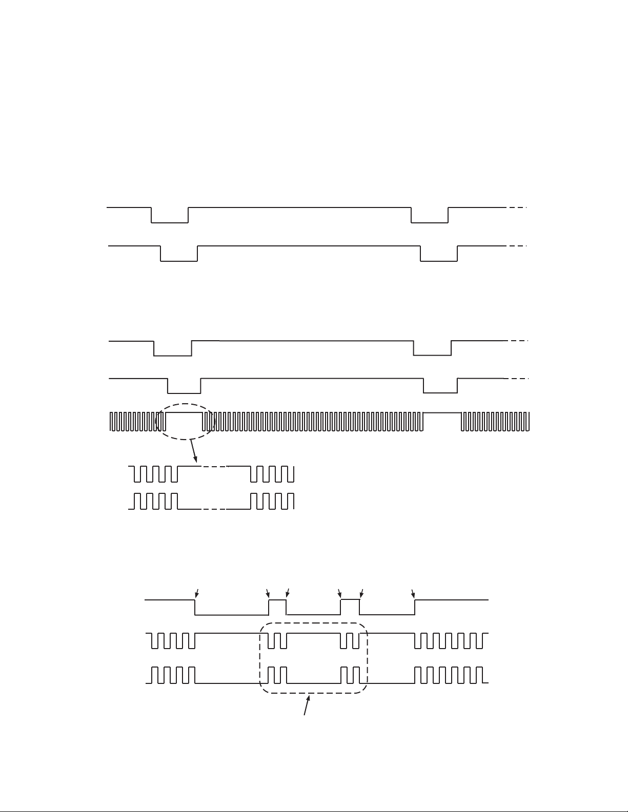
Figure 12. Generating Special HBLK Patterns
–14–
REV. 0
Page 15
AD9991
HORIZONTAL TIMING SEQUENCE EXAMPLE
Figure 13 shows an example CCD layout. The horizontal register
contains 28 dummy pixels, which will occur on each line clocked
from the CCD. In the vertical direction, there are 10 optical
black (OB) lines at the front of the readout and two at the back
of the readout. The horizontal direction has four OB pixels in the
front and 48 in the back.
Figure 14 shows the basic sequence layout, to be used during the
effective pixel readout. The 48 OB pixels at the end of each line
are used for the CLPOB signals. PBLK is optional and is often
used to blank the digital outputs during the noneffective CCD
pixels. HBLK is used during the vertical shift interval.
V
4 OB PIXELS
EFFECTIVE IMAGE AREA
H
HORIZONTAL CCD REGISTER
The HBLK, CLPOB, and PBLK parameters are programmed in
the V-sequence registers.
More elaborate clamping schemes may be used, such as adding
in a separate sequence to clamp during the entire shield OB lines.
This requires confi guring a separate V-sequence for reading out
the OB lines.
2 VERTICAL OB LINES
10 VERTICAL OB LINES
48 OB PIXELS
HD
CCDIN
SHP
SHD
H1/H3
H2/H4
HBLK
PBLK
CLPOB
OPTICAL BLACK
28 DUMMY PIXELS
VERTICAL SHIFT
Figure 13. Example CCD Confi guration
OB
DUMMY
EFFECTIVE PIXELS
Figure 14. Horizontal Sequence Example
OPTICAL BLACK
VERT SHIFT
REV. 0
–15–
Page 16
AD9991
VERTICAL TIMING GENERATION
The AD9991 provides a very fl exible solution for generating
vertical CCD timing, and can support multiple CCDs and different system architectures. The 6-phase vertical transfer clocks
V1–V6 are used to shift each line of pixels into the horizontal
output register of the CCD. The AD9991 allows these outputs to
be individually programmed into various readout confi gurations
using a four step process.
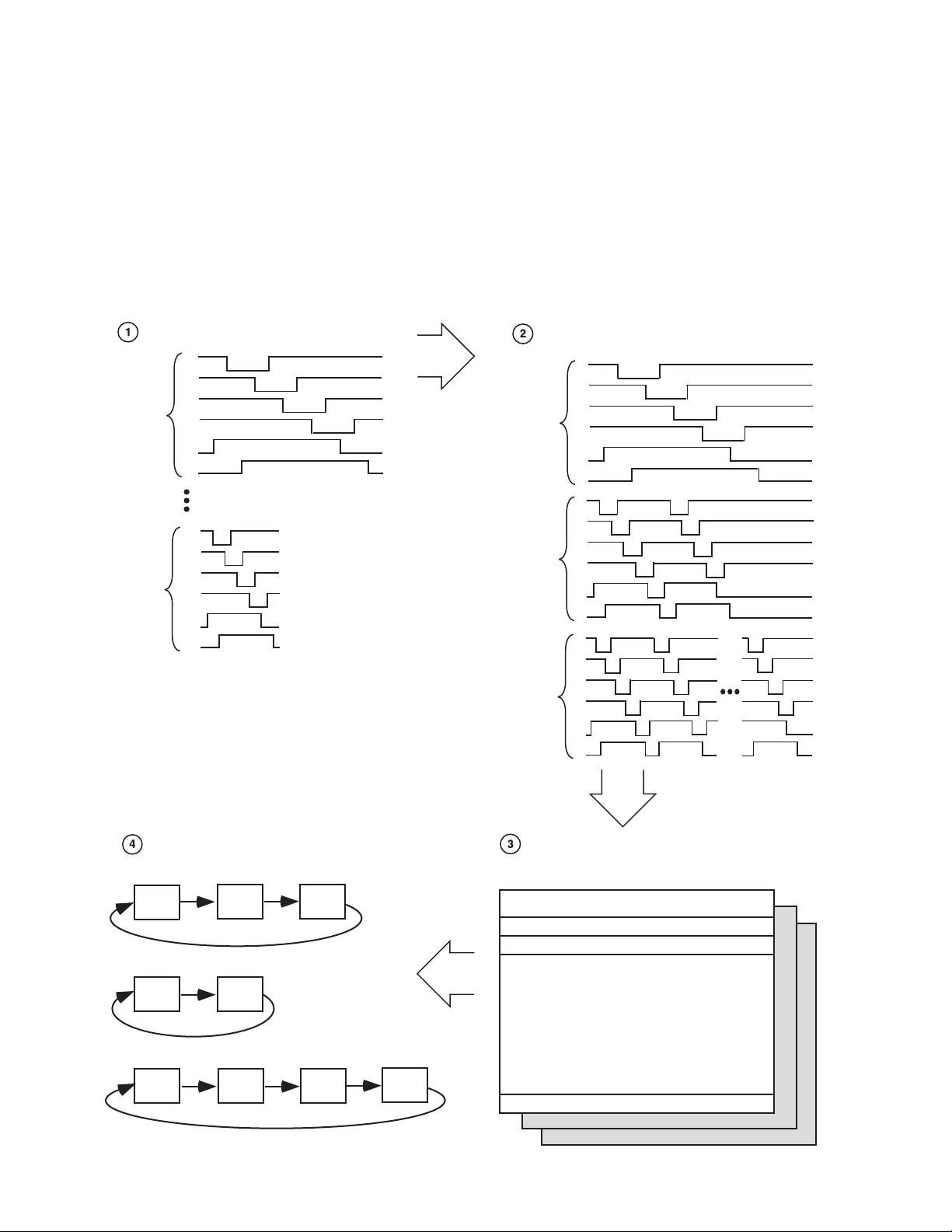
Figure 15 shows an overview of how the vertical timing is generated in four steps. First, the individual pulse patterns for V1–V6
CREATE THE VERTICAL PATTERN GROUPS
(MAXIMUM OF 10 GROUPS).
V1
V2
VPAT 0
VPAT 9
V3
V4
V5
V6
V1
V2
V3
V4
V5
V6
are created by using the vertical pattern group registers. Second,
the V-pattern groups are used to build the sequences, where
additional information is added. Third, the readout for an entire
fi eld is constructed by dividing the fi eld into different regions and
then assigning a sequence to each region. Each fi eld can contain
up to seven different regions to accommodate different steps of
the readout such as high speed line shifts and unique vertical line
transfers. Up to six different fi elds may be created. Finally, the
Mode register allows the different fi elds to be combined into any
order for various readout confi gurations.
BUILD THE V-SEQUENCES BY ADDING LINE START
POSITION, # OF REPEATS, AND HBLK/CLPOB PULSES
(MAXIMUM OF 10 V-SEQUENCES).
V1
V2
V-SEQUENCE 0
(VPAT0, 1 REP)
V-SEQUENCE 1
(VPAT9, 2 REP)
V-SEQUENCE 2
(VPAT9, N REP)
V3
V4
V5
V6
V1
V2
V3
V4
V5
V6
V1
V2
V3
V4
V5
V6
USE THE MODE REGISTER TO CONTROL WHICH FIELDS
ARE USED, AND IN WHAT ORDER
(MAXIMUM OF 7 FIELDS MAY BE COMBINED IN ANY ORDER).
FIELD 0
FIELD 3
FIELD 5
FIELD 1 FIELD 2
FIELD 4
FIELD 1 FIELD 4
FIELD 2
Figure 15. Summary of Vertical Timing Generation
–16–
BUILD EACH FIELD BY DIVIDING INTO DIFFERENT REGIONS,
AND ASSIGNING A DIFFERENT V-SEQUENCE TO EACH
(MAXIMUM OF 7 REGIONS IN EACH FIELD)
(MAXIMUM OF 6 FIELDS).
FIELD 0
REGION 0: USE V-SEQUENCE 2
REGION 0: USE V-SEQUENCE 3
REGION 1: USE V-SEQUENCE 0
REGION 0: USE V-SEQUENCE 3
REGION 2: USE V-SEQUENCE 3
REGION 1: USE V-SEQUENCE 2
REGION 1: USE V-SEQUENCE 2
REGION 3: USE V-SEQUENCE 0
REGION 2: USE V-SEQUENCE 1
REGION 2: USE V-SEQUENCE 1
REGION 4: USE V-SEQUENCE 2
FIELD 1
FIELD 2
REV. 0
Page 17
AD9991
Ve r tical Pattern Groups (VPAT)
The vertical pattern groups defi ne the individual pulse patterns
for each V1–V6 output signal. Table V summarizes the registers
available for generating each of the 10 V-pattern groups. The start
polarity (VPOL) determines the starting polarity of the vertical sequence, and can be programmed high or low for
each V1–V6 output. The fi rst, second, and third toggle position (VTOG1, VTOG2, VTOG3) are the pixel locations within
the line where the pulse transitions. A fourth toggle position
(VTOG4) is also available for V-Pattern Groups 8 and 9. All toggle positions are 12-bit values, allowing their placement anywhere
in the horizontal line. A separate register, VPATSTART, specifi es
the start position of the V-pattern group within the line (see the
Ve rtical Sequences section). The VPATLEN register designates
the total length of the V-pattern group, which will determine the
number of pixels between each of the pattern repetitions, when
repetitions are used (see the Vertical Sequences section).
The FREEZE and RESUME registers are used to temporarily
stop the operation of the V1–V6 outputs. At the pixel location
specifi ed in the FREEZE register, the V1–V6 outputs will be
held static at their current dc state, high or low. The V1–V6
outputs are held until the pixel location specifi ed by RESUME
register. Two sets of FREEZE/RESUME registers are provided, allowing the vertical outputs to be interrupted twice in
the same line. The FREEZE and RESUME positions are programmed in the V-pattern group registers, but are separately
enabled using the VMASK registers, which are described in the
Vertical Sequence section.
Ta b le V. Ver tical Pattern Group Registers
Register Length Range Description
VPOL 1b High/Low Starting Polarity of Each V1–V6 Output
VTOG1 12b 0–4096 Pixel Location First Toggle Position within Line for Each V1–V6 Output
VTOG2 12b 0–4096 Pixel Location Second Toggle Position within Line for Each V1–V6 Output
VTOG3 12b 0–4096 Pixel Location Third Toggle Position within Line for Each V1–V6 Output
VTOG4 12b 0–4096 Pixel Location Fourth Toggle Position, only Available in V-Pattern Groups 8 and 9
VPATLEN 12b 0–4096 Pixels Total Length of Each V-Pattern Group
FREEZE1 12b 0–4096 Pixel Location Holds the V1–V6 Outputs at Their Current Levels (Static DC)
RESUME1 12b 0–4096 Pixel Location Resumes Operation of the V1–V6 Outputs to Finish Their Pattern
FREEZE2 12b 0–4096 Pixel Location Holds the V1–V6 Outputs at Their Current Levels (Static DC)
RESUME2 12b 0–4096 Pixel Location Resumes Operation of the V1–V6 Outputs to Finish Their Pattern
START POSITION OF V-PATTERN GROUP IS PROGRAMMABLE IN V-SEQUENCE REGISTERS
HD
4
V1
V2
V6
PROGRAMMABLE SETTINGS FOR EACH V-PATTERN:
1. START POLARITY
2. FIRST TOGGLE POSITION
3. SECOND TOGGLE POSITION (THIRD TOGGLE POSITION ALSO AVAILABLE, FOURTH TOGGLE POSITION AVAILABLE FOR V-PATTERN GROUPS 8 AND 9)
4. TOTAL PATTERN LENGTH FOR ALL V1–V6 OUTPUTS
1
2
3
1
2
3
1
2
3
Figure 16. Vertical Pattern Group Programmability
REV. 0
–17–
Page 18
AD9991
Ve r tical Sequences (VSEQ)
The vertical sequences are created by selecting one of the 10
V-pattern groups and adding repeats, start position, and horizontal clamping, and blanking information. Up to 10 V-sequences
can be programmed, each using the registers shown in Table VI.
Figure 17 shows how the different registers are used to generate
each V-sequence.
The VPATSEL register selects which V-pattern group will be
used in a given V-sequence. The basic V-pattern group can have
repetitions added, for high speed line shifts or line binning, by
using the VPATREPO and VPATREPE registers. Generally, the
same number of repetitions are programmed into both registers,
but if a different number of repetitions is required on odd and
even lines, separate values may be used for each register (see
the V-Sequence Line Alternation section). The VPATSTART
register specifi es where in the line the V-pattern group will start.
The VMASK register is used in conjunction with the FREEZE/
RESUME registers to enable optional masking of the V-outputs.
Either or both of the FREEZE1/RESUME1 and FREEZE2/
RESUME2 registers can be enabled.
The line length (in pixels) is programmable using the HDLEN
registers. Each V-sequence can have a different line length to
accommodate various image readout techniques. The maximum
number of pixels per line is 4096. Note that the last line of the
fi eld is separately programmable using the HDLAST register
located in the Field register section.
Ta b le VI. V-Sequence Registers (see Tables III and IV for HBLK, CLPOB, PBLK Registers)
Register Length Range Description
VPATSEL 4b 0–9 V-Pattern Group # Selected V-Pattern Group for Each V-Sequence.
VMASK 2b 0–3 Mask Mode Enables the Masking of V1–V6 Outputs at the Locations Specifi ed by
the FREEZE/RESUME Registers. 0 = No Mask, 1 = Enable
FREEZE1/RESUME1, 2 = Enable FREEZE2/RESUME2, 3 = Enable
both 1 and 2.
VPATREPO 12b 0–4095 # of Repeats Number of Repetitions for the V-Pattern Group for Odd Lines.
If no odd/even alternation is required, set equal to VPATREPE.
VPATREPE 12b 0–4095 # of Repeats Number of Repetitions for the V-Pattern Group for Even Lines.
If no odd/even alternation is required, set equal to VPATREPO.
VPATSTART 12b 0–4095 Pixel Location Start Position for the Selected V-Pattern Group.
HDLEN 12b 0–4095 # of Pixels HD Line Length for Lines in Each V-Sequence.
1
HD
2
3
V1–V6
CLPOB
PBLK
HBLK
PROGRAMMABLE SETTINGS FOR EACH V-SEQUENCE:
1. START POSITION IN THE LINE OF SELECTED V-PATTERN GROUP
2. HD LINE LENGTH
3. V-PATTERN SELECT (VPATSEL) TO SELECT ANY V-PATTERN GROUP
4. NUMBER OF REPETITIONS OF THE V-PATTERN GROUP (IF NEEDED)
5. START POLARITY AND TOGGLE POSITIONS FOR CLPOB AND PBLK SIGNALS
6. MASKING POLARITY AND TOGGLE POSITIONS FOR HBLK SIGNAL
V-PATTERN GROUP
6
44
VPAT REP 2
5
Figure 17. V-Sequence Programmability
VPAT REP 3
–18–
REV. 0
Page 19

AD9991
Complete Field: Combining V-Sequences
After the V-sequences have been created, they are combined
to create different readout fi elds. A fi eld consists of up to seven
different regions, and within each region a different V-sequence
can be selected. Figure 18 shows how the sequence change
positions (SCP) designate the line boundry for each region, and
the VSEQSEL registers then select which V-sequence is used
during each region. Registers to control the VSG outputs are
also included in the Field registers.
Table VII summarizes the registers used to create the different
fi elds. Up to six different fi elds can be preprogrammed using all
of the Field registers.
The VEQSEL registers, one for each region, select which of the
10 V-sequences will be active during each region. The SWEEP
registers are used to enable SWEEP mode during any region.
The MULTI registers are used to enable Multiplier mode dur-
ing any region. The SCP registers create the line boundries for
each region. The VDLEN register specifi es the total number of
lines in the fi eld. The total number of pixels per line (HDLEN) is
specifi ed in the V-sequence registers, but the HDLAST register
specifi es the number of pixels in the last line of the fi eld. The
VPATSECOND register is used to add a second V-pattern group
to the V1–6 outputs during the sensor gate (VSG) line.
The SGMASK register is used to enable or disable each individual VSG output. There is a single bit for each VSG output:
setting the bit high will mask the output, setting it low will enable
the output. The SGPAT register assigns one of the four different
SG patterns to each VSG output. The individual SG patterns are
created separately using the SG pattern registers. The SGLINE1
register specifi es which line in the fi eld will contain the VSG outputs. The optional SGLINE2 register allows the same VSG pulses
to be repeated on a different line.
Ta b le VII. Field Registers
Register Length Range Description
VSEQSEL 4b 0–9 V-Sequence # Selected V-Sequence for Each Region in the Field.
SWEEP 1b High/Low Enables Sweep Mode for Each Region, When Set High.
MULTI 1b High/Low Enables Multiplier Mode for Each Region, When Set High.
SCP 12b 0–4095 Line # Sequence Change Position for Each Region.
VDLEN 12b 0–4095 # of Lines Total Number of Lines in Each Field.
HDLAST 12b 0–4095 # of Pixels Length in Pixels of the Last HD Line in Each Field.
VPATSECOND 4b 0–9 V-Pattern Group # Selected V-Pattern Group for Second Pattern Applied During VSG Line.
SGMASK 6b High/Low, Each VSG Set High to Mask Each Individual VSG Output. VSG1 [0], VSG2 [1],
VSG3 [2], VSG4 [3], VSG5 [4].
SGPATSEL 12b 0–3 Pattern #, Each VSG Selects the VSG Pattern Number for Each VSG Output. VSG1 [1:0],
VSG2 [3:2], VSG3 [5:4], VSG4 [7:6], VSG5 [9:8].
SGLINE1 12b 0–4095 Line # Selects the Line in the Field where the VSG Are Active.
SGLINE2 12b 0–4095 Line # Selects a Second Line in the Field to Repeat the VSG Signals.
SGLINE1
SCP 2
REGION 2
VSEQSEL2
SCP 3
REGION 3
VSEQSEL3
SCP 4
SCP 5
REGION 4
VSEQSEL4
SCP 1
VD
REGION 0
HD
V1–V6
VSG
VSEQSEL0
FIELD SETTINGS:
1. SEQUENCE CHANGE POSITIONS (SCP1–6) DEFINE EACH OF THE 7 REGIONS IN THE FIELD.
2. VSEQSEL0–6 SELECTS THE DESIRED V-SEQUENCE (0–9) FOR EACH REGION.
3. SGLINE1 REGISTER SELECTS WHICH HD LINE IN THE FIELD WILL CONTAIN THE SENSOR GATE PULSE(S).
REGION 1
VSEQSEL1
Figure 18. Complete Field is Divided into Regions
SCP 6
REGION 5
VSEQSEL5 VSEQSEL6
REGION 6
REV. 0
–19–
Page 20

AD9991
Generating Line Alternation for V-Sequence and HBLK
During low resolution readout, some CCDs require a different
number of vertical clocks on alternate lines. The AD9991 can
support this by using the VPATREPO and VPATREPE registers. This allows a different number of VPAT repetitions to be
programmed on odd and even lines. Note that only the number
of repeats can be different in odd and even lines, but the VPAT
group remains the same.
Additionally, the HBLK signal can also be alternated for odd
and even lines. When the HBLKALT register is set high, the
HBLK TOG1 and TOG2 positions will be used on odd lines,
while the TOG3–TOG6 positions will be used on even lines.
This allows the HBLK interval to be adjusted on odd and even
lines if needed.
Figure 19 shows an example of VPAT repetition alternation and
HBLK alternation used together. It is also possible to use VPAT
and HBLK alternation separately.
HD
VPATREPO = 2
V1
V2
VPATREPE = 5
Second V-Pattern Group during VSG Active Line
Most CCDs require additional vertical timing during the sensor
gate line. The AD9991 supports the option to output a second
V-pattern group for V1–V6 during the line when the sensor gates
VSG1–VSG5 are active. Figure 20 shows a typical VSG line,
which includes two separate sets of V-pattern groups for V1–V6.
The V-pattern group at the start of the VSG line is selected in the
same manner as the other regions, using the appropriate VSEQSEL register. The second V-pattern group, unique to the VSG
line, is selected using the VPATSECOND register, located with
the Field registers. The start position of the second VPAT group
uses the VPATLEN register from the selected VPAT registers.
Because the VPATLEN register is used as the start position and
not as the VPAT length, it is not possible to program multiple
repetitions for the second VPAT group.
VPATREPO = 2
V6
TOG1 TOG2
HBLK
NOTES
1. THE NUMBER OF REPEATS FOR THE V-PATTERN GROUP MAY BE ALTERNATED ON ODD AND EVEN LINES.
2. THE HBLK TOGGLE POSITIONS MAY BE ALTERNATED BETWEEN ODD AND EVEN LINES IN ORDER TO GENERATE DIFFERENT HBLK PATTERNS FOR ODD/EVEN LINES.
TOG3
TOG4
TOG1 TOG2
Figure 19. Odd/Even Line Alternation of VPAT Repetitions and HBLK Toggle Positions
HD
VSG
V1
V2
V6
START POSITION FOR 2ND VPAT GROUP
USES VPATLEN REGISTER
2ND VPAT GROUP
Figure 20. Example of Second VPAT Group during Sensor Gate Line
–20–
REV. 0
Page 21

AD9991
Sweep Mode Operation
The AD9991 contains an additional mode of vertical timing
operation called Sweep mode. This mode is used to generate a
large number of repetitive pulses that span multiple HD lines.
One example of where this mode is needed is at the start of the
CCD readout operation. At the end of the image exposure but
before the image is transferred by the sensor gate pulses, the
vertical interline CCD registers should be free of all charge. This
can be accomplished by quickly shifting out any charge using
a long series of pulses from the V1–V6 outputs. Depending on
the vertical resolution of the CCD, up to 2,000 or 3,000 clock
cycles will be needed to shift the charge out of each vertical CCD
line. This operation will span across multiple HD line lengths.
Normally, the AD9991 vertical timing must be contained within
one HD line length, but when Sweep mode is enabled, the HD
boundaries will be ignored until the region is fi nished. To enable
Sweep mode within any region, program the appropriate
SWEEP register to High.
Figure 21 shows an example of the Sweep mode operation. The
number of vertical pulses needed will depend on the vertical
resolution of the CCD. The V1–V6 output signals are generated using the V-pattern registers (shown in Table VII). A single
pulse is created using the polarity and toggle position registers.
The number of repetitions is then programmed to match the
number of vertical shifts required by the CCD. Repetitions are
programmed in the V-sequence registers using the VPATREP
registers. This produces a pulse train of the appropriate length.
Normally, the pulse train would be truncated at the end of the
HD line length, but with Sweep mode enabled for this region,
the HD boundaries will be ignored. In Figure 21, the Sweep
region occupies 23 HD lines. After the Sweep mode region is
completed, in the next region, normal sequence operation will
resume. When using Sweep mode, be sure to set the region
boundries (using the sequence change positions) to the appropriate lines to prevent the Sweep operation from overlapping the
next V-sequence.
Multiplier Mode
To generate very wide vertical timing pulses, a vertical region
may be confi gured into a multiplier region. This mode uses
the V-pattern registers in a slightly different manner. Multiplier
mode can be used to support unusual CCD timing requirements,
such as vertical pulses that are wider than a single HD line length.
The start polarity and toggle positions are still used in the same
manner as the standard VPAT group programming, but the
VPATLEN is used differently. Instead of using the pixel counter
(HD counter) to specify the toggle position locations (VTOG1,
2, 3) of the VPAT group, the VPATLEN is multiplied with the
VTOG position to allow very long pulses to be generated. To calculate the exact toggle position, counted in pixels after the start
position, use the equation
Multiplier Mode Toggle Position = VTOG VPATLEN
Because the VTOG register is multiplied by VPATLEN,
the resolution of the toggle position placement is reduced. If
VPATLEN = 4, the toggle position accuracy is now reduced
to 4-pixel steps instead of single pixel steps. Table VIII summarizes how the VPAT group registers are used in Multiplier
mode operation. In Multiplier mode, the VPATREPO and
VPATREPE registers should always be programmed to the same
value as the highest toggle position.
VD
HD
V1–V6
LINE 0 LINE 1
REGION 0 REGION 2
Figure 21. Example of Sweep Region for High Speed Vertical Shift
SCP 1 SCP 2
LINE 24 LINE 25LINE 2
REGION 1: SWEEP REGION
Ta b le VIII. Multiplier Mode Register Parameters
Register Length Range Description
MULTI 1b High/Low High enables Multiplier mode.
VPOL 1b High/Low Starting Polarity of V1–V6 Signal in Each VPAT Group.
VTOG1 12b 0–4095 Pixel Location First Toggle Position for V1–V6 Signal in Each VPAT Group.
VTOG2 12b 0–4095 Pixel Location Second Toggle Position for V1–V6 Signal in Each VPAT Group.
VTOG3 12b 0–4095 Pixel Location Third Toggle Position for V1–V6 Signal in Each VPAT Group.
VPATLEN 10b 0–1023 Pixels Used as Multiplier Factor for Toggle Position Counter.
VPATREP 12b 0–4096 VPATREPE/VPATREPO should be set to the same value as TOG2 or 3.
REV. 0
–21–
Page 22

AD9991
The example shown in Figure 22 illustrates this operation. The
fi rst toggle position is 2, and the second toggle position is 9. In
non-Multiplier mode, this would cause the V-sequence to toggle
at pixel 2 and then pixel 9 within a single HD line. However,
toggle positions are now multiplied by the VTPLEN = 4, so the
fi rst toggle occurs at pixel count 8, and the second toggle occurs
at pixel count 36. Sweep mode has also been enabled to allow the
toggle positions to cross the HD line boundaries.
Ve r tical Sensor Gate (Shift Gate) Patterns
In an Interline CCD, the vertical sensor gates (VSG) are used
to transfer the pixel charges from the light-sensitive image area
into light-shielded vertical registers. From the light-shield vertical registers, the image is then read out line-by-line by using the
vertical transfer pulses V1–V6 in conjunction with the high speed
horizontal clocks.
START POSITION OF VPAT GROUP IS STILL PROGRAMMED IN THE V-SEQUENCE REGISTERS
HD
55
VPATLEN
PIXEL
NUMBER
3
123412341234123412341234123412 3412341234
1 2345678 910111213141516171819202122232425262728293031323334353637383940
Table IX contains the summary of the VSG pattern registers. The
AD9991 has fi ve VSG outputs, VSG1–VSG5. Each of the outputs can be assigned to one of four programmed patterns by using
the SGPATSEL registers. Each pattern is generated in a similar
manner as the V-pattern groups, with a programmable start polarity (SGPOL), fi rst toggle position (SGTOG1), and second toggle
position (SGTOG2). The active line where the VSG1–VSG5
pulses occur is programmable using the SGLINE1 and SGLINE2
registers. Additionally, any of the VSG1–VSG5 pulses may be
individually disabled by using the SGMASK register. The individual masking allows all of the SG patterns to be preprogrammed,
and the appropriate pulses for the different fi elds can be separately
enabled. For maximum fl exibility, the SGPATSEL, SGMASK,
and SGLINE registers are separately programmable for each fi eld.
More detail is given in the Complete Field section.
4
V1–V6
1
MULTIPLIER MODE V-PATTERN GROUP PROPERTIES:
1. START POLARITY (ABOVE: STARTPOL = 0)
2. FIRST, SECOND, AND THIRD TOGGLE POSITIONS (ABOVE: VTOG1 = 2, VTOG2 = 9)
3. LENGTH OF VPAT COUNTER (ABOVE: VPATLEN = 4). THIS IS THE MINIMUM RESOLUTION FOR TOGGLE POSITION CHANGES.
4. TOGGLE POSITIONS OCCUR AT LOCATION EQUAL TO (VTOG ⴛ VPATLEN)
5. IF SWEEP REGION IS ENABLED, THE V-PULSES MAY ALSO CROSS THE HD BOUNDRIES, AS SHOWN ABOVE
2
4
2
Figure 22. Example of Multiplier Region for Wide Vertical Pulse Timing
Ta b le IX. VSG Pattern Registers (also see Field Registers in Table VII)
Register Length Range Description
SGPOL 1b High/Low Sensor Gate Starting Polarity for SG Pattern 0–3
SGTOG1 12b 0–4095 Pixel Location First Toggle Position for SG Pattern 0–3
SGTOG2 12b 0–4095 Pixel Location Second Toggle Position for SG Pattern 0–3
VD
4
HD
VSG PATTERNS
12 3
PROGRAMMABLE SETTINGS FOR EACH PATTERN:
1. START POLARITY OF PULSE
2. FIRST TOGGLE POSITION
3. SECOND TOGGLE POSITION
4. ACTIVE LINE FOR VSG PULSES WITHIN THE FIELD (PROGRAMMABLE IN THE FIELD REGISTER, NOT FOR EACH PATTERN)
Figure 23. Vertical Sensor Gate Pulse Placement
–22–
REV. 0
Page 23

AD9991
MODE Register
The MODE register is a single register that selects the fi eld timing of the AD9991. Typically, all of the fi eld, V-sequence, and
V-pattern group information is programmed into the AD9991
at startup. During operation, the MODE register allows the user
to select any combination of fi eld timing to meet the current
requirements of the system. The advantage of using the MODE
register in conjunction with preprogrammed timing is that it
greatly reduces the system programming requirements during
camera operation. Only a few register writes are required when
the camera operating mode is changed, rather than having to
write in all of the vertical timing information with each camera
mode change.
A basic still camera application might require fi ve different
fi elds of vertical timing: one for draft mode operation, one for
autofocusing, and three for still image readout. All of the register timing information for the fi ve fi elds would be loaded at
startup. Then, during camera operation, the MODE register
would select which fi eld timing would be active, depending on
how the camera was being used.
Table X shows how the MODE register bits are used. The three
MSBs, D23–D21, are used to specify how many total fi elds will
be used. Any value from 1 to 7 can be selected using these three
bits. The remaining register bits are divided into 3-bit sections to
select which of the six fi elds are used and in which order. Up to
seven fi elds may be used in a single MODE write. The AD9991
will start with the Field timing specifi ed by the fi rst Field bits,
and on the next VD will switch to the timing specifi ed by the
second Field bits, and so on.
After completing the total number of fi elds specifi ed in Bits
D23 to D21, the AD9991 will repeat by starting at the fi rst
Field again. This will continue until a new write to the MODE
register occurs. Figure 24 shows example MODE register settings for different fi eld confi gurations.
Ta b le X. MODE Register Data Bit Breakdown (D23 = MSB)
D23 22 21 20 19 18 17 16 15 14 13 12 11 10 9 8 7 6 5 4 3 2 1 D0
Total Number of 7th Field 6th Field 5th Field 4th Field 3rd Field 2nd Field 1st Field
Fields to Use. 0 = Field 0 0 = Field 0 0 = Field 0 0 = Field 0 0 = Field 0 0 = Field 0 0 = Field 0
1 = 1st Field Only 5 = Field 5 5 = Field 5 5 = Field 5 5 = Field 5 5 = Field 5 5 = Field 5 5 = Field 5
7 = All 7 Fields 6, 7 = Invalid 6, 7 = Invalid 6, 7 = Invalid 6, 7 = Invalid 6, 7 = Invalid 6, 7 = Invalid 6, 7 = Invalid
0 = Invalid
EXAMPLE 1:
TOTAL FIELDS = 3, 1ST FIELD = FIELD 0, 2ND FIELD = FIELD 1, 3RD FIELD = FIELD 2
MODE REGISTER CONTENTS = 0x600088
FIELD 0
EXAMPLE 2:
TOTAL FIELDS = 2, 1ST FIELD = FIELD 3, 2ND FIELD = FIELD 4
MODE REGISTER CONTENTS = 0x400023
FIELD 3
EXAMPLE 3:
TOTAL FIELDS = 4, 1ST FIELD = FIELD 5, 2ND FIELD = FIELD 1, 3RD FIELD = FIELD 4, 4TH FIELD = FIELD 2
MODE REGISTER CONTENTS = 0x80050D
FIELD 5
FIELD 1 FIELD 2
FIELD 4
FIELD 1 FIELD 4
FIELD 2
Figure 24. Using the MODE Register to Select Field Timing
REV. 0
–23–
Page 24

AD9991
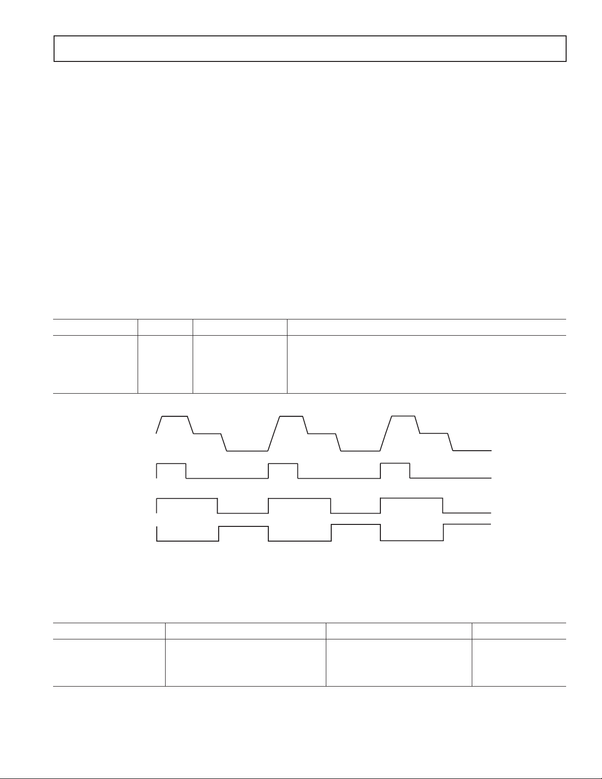
VERTICAL TIMING EXAMPLE
To better understand how the AD9991 vertical timing generation
is used, consider the example CCD timing chart in Figure 25.
This particular example illustrates a CCD using a general 3-fi eld
readout technique. As described in the previous Field section,
each readout fi eld should be divided into separate regions to
perform each step of the readout. The sequence change positions (SCP) determine the line boundaries for each region, and
the VSEQSEL registers will then assign a particular V-sequence
to each region. The V-sequences will contain the specifi c timing
information required in each region: V1–V6 pulses (using VPAT
groups), HBLK/CLPOB timing, and VSG patterns for the SG
active lines.
This particular timing example requires four regions for each
of the three fi elds, labeled Region 0, Region 1, Region 2, and
Region 3. Because the AD9991 allows up to six individual fi elds
to be programmed, the Field 0, Field 1, and Field 2 registers can
be used to meet the requirements of this timing example. The
four regions for each fi eld are very similar in this example, but
the individual registers for each fi eld allow fl exibility to accommodate other timing charts.
Region 0 is a high speed vertical shift region. Sweep mode can be
used to generate this timing operation, with the desired number
of high speed vertical pulses needed to clear any charge from the
CCD’s vertical registers.
Region 1 consists of only two lines, and uses standard single line
vertical shift timing. The timing of this region area will be the
same as the timing in Region 3.
Region 2 is the sensor gate line, where the VSG pulses transfer the
image into the vertical CCD registers. This region may require the
use of the second V-pattern group for SG active line.
Region 3 also uses the standard single line vertical shift timing,
the same timing as Region 1.
In summary, four regions are required in each of the three fi elds.
The timing for Regions 1 and 3 is essentially the same, reducing
the complexity of the register programming.
Other registers will need to be used during the actual readout
operation, such as the MODE register, shutter control registers
(TRIGGER, SUBCK, VSUB, MSHUT, STROBE), and the AFE
gain register. These registers will be explained in other examples.
Important Note About Signal Polarities
When programming the AD9991 to generate the V1–V6,
VSG1–VSG5, and SUBCK signals, it is important to note that
the V-driver circuit usually inverts these signals. Carefully check
the required timing signals needed at the input and output of
the V-driver circuit being used, and adjust the polarities of the
AD9991 outputs accordingly.
–24–
REV. 0
Page 25

THIRD FIELD READOUT
OPEN
AD9991
n
n– 3
21
18
15
12
9
6
3
FIELD 2
REGION 1 REGION 2
REGION 0 REGION 3
n–1
n–4
20
17
14
11
8
5
2
SECOND FIELD READOUT
FIRST FIELD READOUT
)
EXP
t
EXPOSURE (
CLOSED
OPEN
FIELD 1
REGION 1 REGION 2
REGION 0 REGION 3
n–2
n–5
16
13
10
7
4
1
Figure 25. CCD Timing Example: Dividing Each Field into Regions
FIELD 0
REGION 1 REGION 2
REGION 0 REGION 3
REV. 0
VD
HD
V3
V1
V2
V4
V5
V6
SUBCK
MSHUT
VSUB
CCD
OUT
–25–
Page 26

AD9991
SHUTTER TIMING CONTROL
The CCD image exposure time is controlled by the substrate
clock signal (SUBCK), which pulses the CCD substrate to clear
out accumulated charge. The AD9991 supports three types of
electronic shuttering: normal shutter, high precision shutter,
and low speed shutter. Along with the SUBCK pulse placement,
the AD9991 can accommodate different readout confi gurations
to further suppress the SUBCK pulses during multiple fi eld
readouts. The AD9991 also provides programmable outputs to
control an external mechanical shutter (MSHUT), strobe/fl ash
(STROBE), and the CCD bias select signal (VSUB).
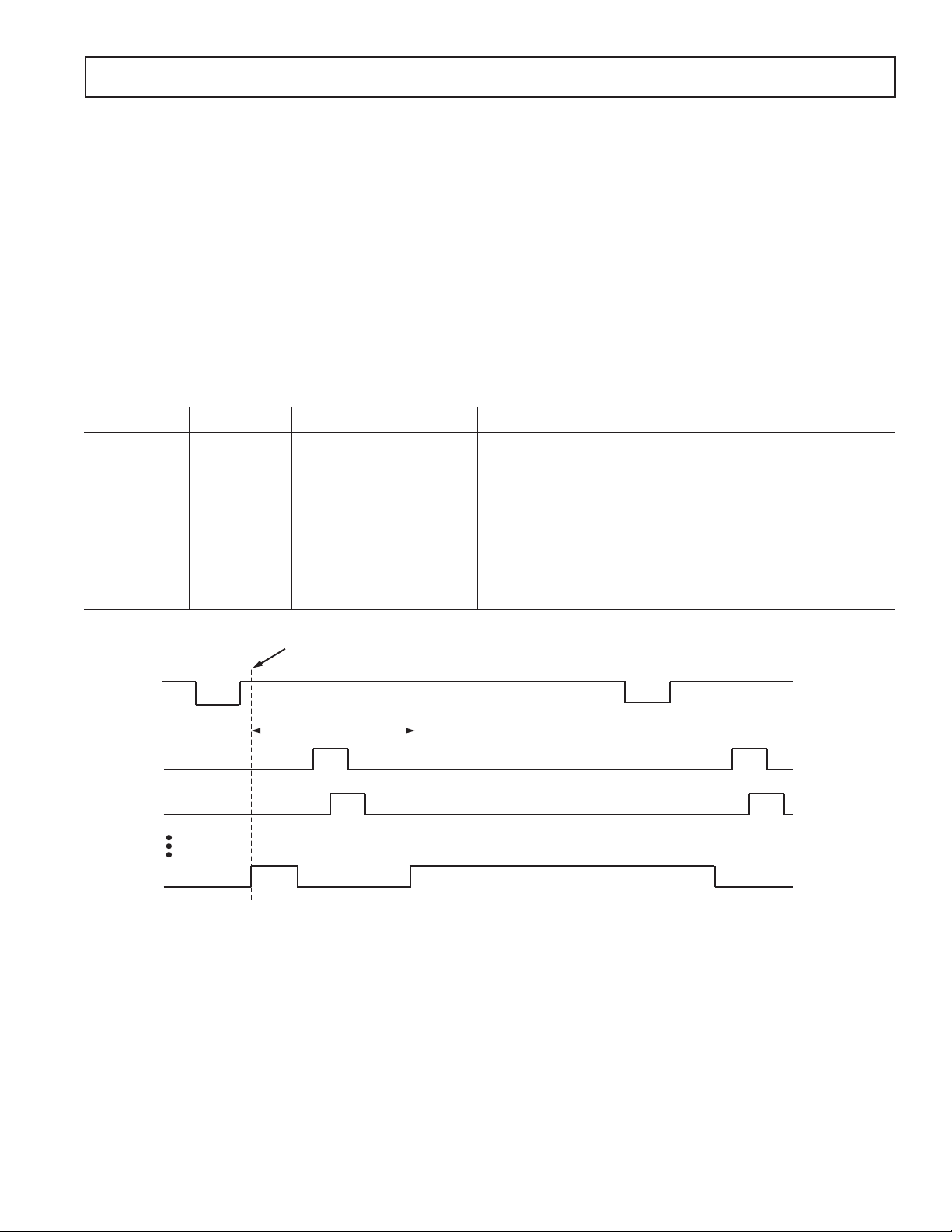
Normal Shutter Operation
By default, the AD9991 is always operating in the normal shutter
confi guration in which the SUBCK signal is pulsing in every VD
fi eld (see Figure 26). The SUBCK pulse occurs once per line,
and the total number of repetitions within the fi eld will determine
the length of the exposure time. The SUBCK pulse polarity
and toggle positions within a line are programmable using the
SUBCKPOL and SUBCK1TOG registers (see Table XI).
The number of SUBCK pulses per fi eld is programmed in the
SUBCKNUM register (addr. 0x63).
As shown in Figure 26, the SUBCK pulses will always begin
in the line following the SG active line, which is specifi ed in
the SGACTLINE registers for each fi eld. The SUBCKPOL,
SUBCK1TOG, SUBCK2TOG, SUBCKNUM, and SUBCKSUPPRESS registers are updated at the start of the line after the
sensor gate line, as described in the Serial Update section.
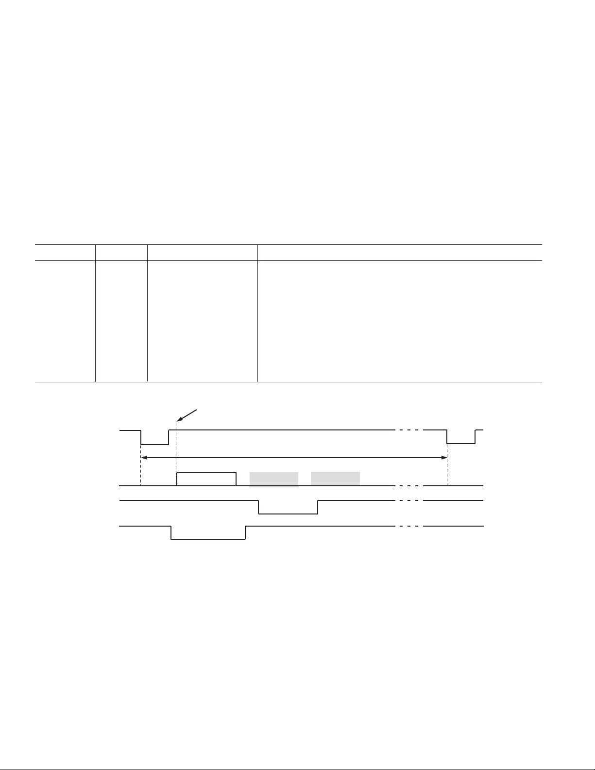
High Precision Shutter Operation
High precision shuttering is used in the same manner as normal shuttering, but uses an additional register to control the
very last SUBCK pulse. In this mode, the SUBCK still pulses
once per line, but the last SUBCK in the fi eld will have an
additional SUBCK pulse whose location is determined by the
SUBCK2TOG register, as shown in Figure 27. Finer resolution
of the exposure time is possible using this mode. Leaving the
SUBCK2TOG register set to max value (0xFFFFFF) will disable
the last SUBCK pulse (default setting).
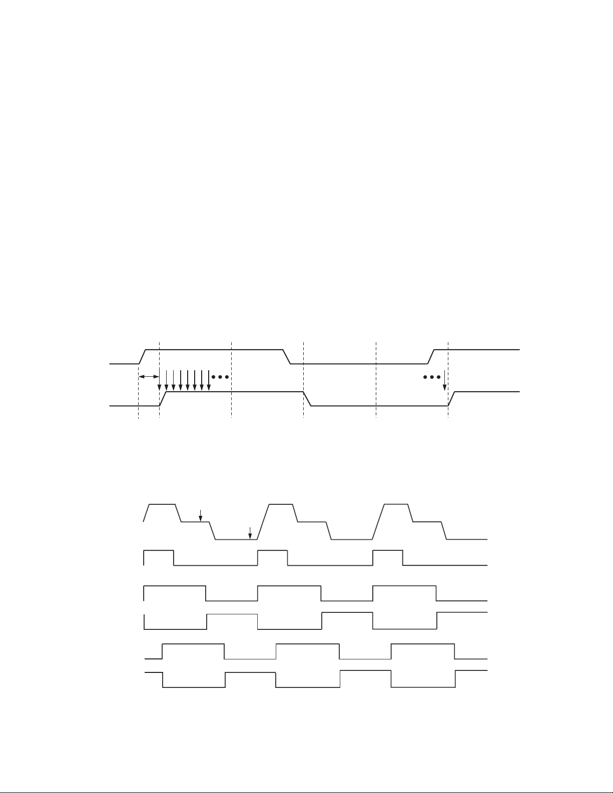
Low Speed Shutter Operation
Normal and high precision shutter operations are used when
the exposure time is less than one fi eld long. For long exposure
times greater than one fi eld interval, low speed shutter operation is used. The AD9991 uses a separate exposure counter to
achieve long exposure times. The number of fi elds for the low
speed shutter operation is specifi ed in the EXPOSURE register
(addr. 0x62). As shown in Figure 28, this shutter mode will
suppress the SUBCK and VSG outputs for up to 4095 fi elds
(VD periods). The VD and HD outputs may be suppressed
during the exposure period by programming the VDHDOFF
register to 1.
To generate a low speed shutter operation, it is necessary to trigger the start of the long exposure by writing to the TRIGGER
register bit D3. When this bit is set High, the AD9991 will begin
an exposure operation at the next VD edge. If a value greater than
zero is specifi ed in the EXPOSURE register, the AD9991 will
suppress the SUBCK output on subsequent fi elds.
VD
HD
VSG
SUBCK
SUBCK PROGRAMMABLE SETTINGS:
1. PULSE POLARITY USING THE SUBCKPOL REGISTER
2. NUMBER OF PULSES WITHIN THE FIELD USING THE SUBCKNUM REGISTER (SUBCKNUM = 3 IN THE ABOVE FIGURE)
3. PIXEL LOCATION OF PULSE WITHIN THE LINE AND PULSEWIDTH PROGRAMMED USING SUBCK1 TOGGLE POSITION REGISTER
t
EXP
Figure 26. Normal Shutter Mode
VD
HD
VSG
SUBCK
NOTES
1. SECOND SUBCK PULSE IS ADDED IN THE LAST SUBCK LINE.
2. LOCATION OF 2ND PULSE IS FULLY PROGRAMMABLE USING THE SUBCK2 TOGGLE POSITION REGISTER.
t
EXP
t
EXP
t
EXP
Figure 27. High Precision Shutter Mode
–26–
REV. 0
Page 27

AD9991
If the exposure is generated using the TRIGGER register and the
EXPOSURE register is set to zero, the behavior of the SUBCK
will not be any different than the normal shutter or high precision
shutter operations, in which the TRIGGER register is not used.
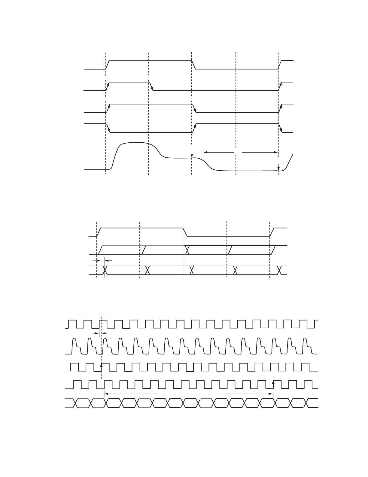
SUBCK Suppression
Normally, the SUBCKs will begin to pulse on the line following
the sensor gate line (VSG). With some CCDs, the SUBCK pulse
needs to be suppressed for one or more lines following the VSG
line. The SUBCKSUPPRESS register allows for suppression of
the SUBCK pulses for additional lines following the VSG line.
Readout after Exposure
After the exposure, the readout of the CCD data occurs, beginning
with the sensor gate (VSG) operation. By default, the AD9991 is
generating the VSG pulses in every fi eld. In the case where only a
single exposure and single readout frame are needed, such as the
CCD’s preview mode, the VSG and SUBCK pulses can be operating in every fi eld.
However in many cases, during readout the SUBCK output
needs to be further suppressed until the readout is completed.
The READOUT register specifi es the number of additional
fi elds after the exposure to continue the suppression of SUBCK.
READOUT can be programmed for zero to seven additional
fi elds, and should be preprogrammed at startup, not at the same
time as the exposure write. A typical interlaced CCD frame read-
out mode will generally require two additional fi elds of SUBCK
suppression (READOUT = 2). A 3-fi eld, 6-phase CCD will
require three additional fi elds of SUBCK suppression after the
readout begins (READOUT = 3).
If the SUBCK output is required to start back up during the last
fi eld of readout, simply program the READOUT register to one
less than the total number of CCD readout fi elds.
Like the exposure operation, the readout operation must be triggered by using the TRIGGER register.
Using the TRIGGER Register
As described previously, by default the AD9991 will output the
SUBCK and VSG signals on every fi eld. This works well for continuous single fi eld exposure and readout operations, such as the
CCD’s live preview mode. However, if the CCD requires a longer
exposure time, or if multiple readout fi elds are needed, then the
TRIGGER register is needed to initiate specifi c exposure and
readout sequences.
Typically, the exposure and readout bits in the TRIGGER
register are used together. This will initiate a complete exposureplus-readout operation. Once the exposure has been completed,
the readout will automatically occur. The values in the EXPOSURE and READOUT registers will determine the length of
each operation.
TRIGGER
EXPOSURE
VD
VSG
SUBCK
NOTES
1. SUBCK MAY BE SUPPRESSED FOR MULTIPLE FIELDS BY PROGRAMMING THE EXPOSURE REGISTER GREATER THAN ZERO.
2. ABOVE EXAMPLE USES EXPOSURE = 1.
3. TRIGGER REGISTER MUST ALSO BE USED TO START THE LOW SPEED EXPOSURE.
4. VD/HD OUTPUTS MAY ALSO BE SUPPRESSED USING THE VDHDOFF REGISTER = 1.
Figure 28. Low Speed Shutter Mode Using EXPOSURE Register
Ta b le XI. Shutter Mode Register Parameters
t
EXP
Register Length Range Description
TRIGGER 5b On/Off for Five Signals Trigger for VSUB [0], MSHUT [1], STROBE [2], Exposure [3],
and Readout Start [4]
READOUT 3b 0–7 # of Fields Number of Fields to Suppress SUBCK after Exposure
EXPOSURE 12b 0–4095 # of Fields Number of Fields to Suppress to SUBCK and VSG during
Exposure Time (Low Speed Shutter)
VDHDOFF 1b On/Off Disable VD/HD Output during Exposure (1 = On, 0 = Off)
SUBCKPOL* 1b High/Low SUBCK Start Polarity for SUBCK1 and SUBCK2
SUBCK1TOG* 24b 0–4095 Pixel Locations Toggle Positions for First SUBCK Pulse (Normal Shutter)
SUBCK2TOG* 24b 0–4095 Pixel Locations Toggle Positions for Second SUBCK Pulse in Last Line
(High Precision)
SUBCKNUM* 12b 1–4095 # of Pulses Total Number of SUBCKs per Field, at One Pulse per Line
SUBCKSUPPRESS* 12b 0–4095 # of Pulses Number of Lines to Further Suppress SUBCK after the VSG Line
*Register is not VD updated, but is updated at the start of line after sensor gate line.
REV. 0
–27–
Page 28

AD9991
It is possible to independently trigger the readout operation
without triggering the exposure operation. This will cause the
readout to occur at the next VD, and the SUBCK output will be
suppressed according to the value of the READOUT register.
The TRIGGER register is also used to control the STROBE,
MSHUT, and VSUB signal transitions. Each of these signals are
individually controlled, although they will be dependent on the
triggering of the exposure and readout operation.
See Figure 32 for a complete example of triggering the exposure
and readout operations.
VSUB Control
The CCD readout bias (VSUB) can be programmed to accommodate different CCDs. Figure 29 shows two different modes
that are available. In Mode 0, VSUB goes active during the fi eld
of the last SUBCK when the exposure begins. The On position
(rising edge in Figure 29) is programmable to any line within
TRIGGER
VSUB
VD
VSG1
t
EXP
the fi eld. VSUB will remain active until the end of the image
readout. In Mode 1, the VSUB is not activated until the start of
the readout.
An additional function called VSUB KEEP-ON is also available.
When this bit is set high, the VSUB output will remain on (active)
even after the readout has fi nished. To disable the VSUB at a later
time, set this bit back to low.
MSHUT and STROBE Control
MSHUT and STROBE operation is shown in Figures 30, 31,
and 32. Table XII shows the register parameters for controlling
the MSHUT and STROBE outputs. The MSHUT output is
switched on with the MSHUTON registers, and will remain on
until the location specifi ed in the MSHUTOFF registers. The
location of MSHUTOFF is fully programmable to anywhere
within the exposure period, using the FD (fi eld), LN (line), and
PX (pixel) registers. The STROBE pulse is defi ned by the on and
READOUT
SUBCK
2
VSUB
1
VSUB OPERATION:
1. ACTIVE POLARITY IS POLARITY (ABOVE EXAMPLE IS VSUB ACTIVE HIGH).
2. ON POSITION IS PROGRAMMABLE. MODE 0 TURNS ON AT THE START OF EXPOSURE, MODE 1 TURNS ON AT THE START OF READOUT.
3. OFF POSITION OCCURS AT END OF READOUT.
4. OPTIONAL VSUB KEEP-ON MODE WILL LEAVE THE VSUB ACTIVE AT THE END OF READOUT.
MODE 0
2
MODE 1
Figure 29. VSUB Programmability
TRIGGER
EXPOSURE
AND MSHUT
VD
VSG
SUBCK
MSHUT
2
1
MSHUT PROGRAMMABLE SETTINGS:
1. ACTIVE POLARITY.
2. ON POSITION IS VD UPDATED AND MAY BE SWITCHED ON AT ANY TIME.
3. OFF POSITION CAN BE PROGRAMMED ANYWHERE FROM THE FIELD OF LAST SUBCK UNTIL THE FIELD BEFORE READOUT.
t
EXP
3
4
3
Figure 30. MSHUT Output Programmability
–28–
REV. 0
Page 29

AD9991
off positions. STROBON_FD is the fi eld in which the STROBE
is turned on, measured from the fi eld containing the last SUBCK
before exposure begins. The STROBON_ LN PX register gives
the line and pixel positions with respect to STROBON_FD. The
STROBE off position is programmable to any fi eld, line, and
pixel location with respect to the fi eld of the last SUBCK.
TRIGGER Register Limitations
While the TRIGGER register can be used to perform a complete
exposure and readout operation, there are limitations on its use.
Once an exposure-plus-readout operation has been triggered,
another exposure/readout operation cannot be triggered right
away. There must be at least one idle fi eld (VD intervals) before
the next exposure/readout can be triggered.
TRIGGER
EXPOSURE
AND STROBE
VD
VSG
SUBCK
The same limitation applies to the triggering of the MSHUT
signal. There must be at least one idle fi eld after the completion
of the MSHUT OFF operation before another MSHUT OFF
operation may be programmed.
The VSUB trigger requires two idle fi elds between exposure/
readout operations in order to ensure proper VSUB on/off triggering. If the VSUB signal is not required to be turned on and
off in between each successive exposure/readout operation, this
limitation can be ignored. The VSUB Keep-On mode is useful
when successive exposure/readout operations are required.
t
EXP
STROBE
1
STROBE PROGRAMMABLE SETTINGS:
1. ACTIVE POLARITY.
2. ON POSITION IS PROGRAMMABLE IN ANY FIELD DURING THE EXPOSURE TIME (WITH RESPECT TO THE FIELD CONTAINING THE LAST SUBCK).
3. OFF POSITION IS PROGRAMMABLE IN ANY FIELD DURING THE EXPOSURE TIME.
2
3
Figure 31. STROBE Output Programmability
Ta b le XII. VSUB, MSHUT, and STROBE Register Parameters
Register Length Range Description
VSUBMODE[0] 1b High/Low VSUB Mode (0 = Mode 0, 1 = Mode 1) (See Figure 29).
VSUBMODE[1] 1b High/Low VSUB Keep-On Mode. VSUB will stay active after readout
when set high.
VSUBON[11:0] 12b 0–4095 Line Location VSUB On Position. Active starting in any line of fi eld.
VSUBON[12] 1b High/Low VSUB Active Polarity.
MSHUTPOL[0] 1b High/Low MSHUT Active Polarity.
MSHUTPOL[1] 1b On/Off MSHUT Manual Enable (1 = Active or Open).
MSHUTON 24b 0–4095 Line/Pix Location MSHUT On Position Line [11:0] and Pixel [23:12] Location.
MSHUTOFF_FD 12b 0–4095 Field Location Field Location to Switch Off MSHUT (Inactive or Closed).
MSHUTOFF_LNPX 24b 0–4095 Line/Pix Location Line/Pixel Position to Switch Off MSHUT (Inactive or Closed).
STROBPOL 1b High/Low STROBE Active Polarity.
STROBON_FD 12b 0–4095 Field Location STROBE ON Field Location, with Respect to Last SUBCK Field.
STROBON_LNPX 24b 0–4095 Line/Pix Location STROBE ON Line/Pixel Position.
STROBOFF_FD 12b 0–4095 Field Location STROBE OFF Field Location, with Respect to Last SUBCK Field.
STROBOFF_LNPX 24b 0–4095 Line/Pix Location STROBE OFF Line/Pixel Position.
REV. 0
–29–
Page 30

AD9991
DRAFT IMAGEDRAFT IMAGE
OPEN
STILL IMAGE READOUT
ters (addr 0x6B and 0x6C).
STILL IMAGE 2ND FIELD STILL IMAGE 3RD FIELD
STILL IMAGE 1ST FIELD
CLOSED
OPEN
EXP
t
MODE 1
MODE 0
and OFF registers (addr 0x6E to 0x71).
6. The next VD falling edge will automatically start the fi rst readout fi eld.
4. STROBE output turns on and off at the location specifi ed in the STROBEON
5. MSHUT output turns off at the location specifi ed in the MSHUTOFF regis-
7. The next VD falling edge will automatically start the second readout fi eld.
8. The next VD falling edge will automatically start the third readout fi eld.
9. Write to the MODE register to reconfi gure the single Draft mode fi eld timing.
Write to the MSHUTON register (addr 0x6A) to open the mechanical shutter.
10. VD/HD falling edge will update the serial writes from 9.
VSG outputs return to Draft mode timing.
SUBCK output resumes operation.
MSHUT output returns to the on position (active or open).
VSUB output returns to the off position (inactive).
Figure 32. Example of Exposure and Still Image Readout Using Shutter Signals and Mode Register
DRAFT IMAGE
SERIAL
WRITES
VD
VSG
SUBCK
STROBE
MSHUT
VSUB
SHUTTER
MECHANICAL
–30–
CCD
OUT
to further suppress SUBCK while the CCD data is read out. In this example,
READOUT = 3.
1. Write to the READOUT register (addr 0x61) to specify the number of fi elds
Write to the EXPOSURE register (addr 0x62) to specify the number of fi elds
to suppress SUBCK and VSG outputs during exposure. In this example,
EXPOSURE = 1.
and VSUB signals, and to start the exposure/readout operation. To trigger all
of these events (as in Figure 32), set the register TRIGGER = 31. Readout will
Write to the TRIGGER register (addr 0x60) to enable the STROBE, MSHUT,
automatically occur after the exposure period is fi nished.
Write to the MODE register (0x1B) to confi gure the next fi ve fi elds. The fi rst
two fi elds during exposure are the same as the current draft mode fi elds, and the
following three fi elds are the still frame readout fi elds. The registers for the Draft
mode fi eld and the three readout fi elds have already been programmed.
2. VD/HD falling edge will update the serial writes from 1.
the VSUBON register (addr 0x68).
3. If VSUB mode = 0 (addr 0x67), VSUB output turns on at the line specifi ed in
REV. 0
Page 31

CCDIN
DC RESTORE
1.5V
SHP
CDS
SHP
SHD
SHD
DOUT
PHASE
6dB–42dB
VGA
VGA GAIN
REGISTER
CLPOB
PBLK
DAC
1.0V 2.0V
INTERNAL
V
REF
10-BIT
ADC
OPTICAL BLACK
CLAMP
DIGITAL
FILTER
REFTREFB
2V FULL SCALE
CLAMP LEVEL
REGISTER
CLPOB
8
AD9991
OUTPUT
DATA
LATCH
PBLK
DOUT
PHASE
AD9991
10
DOUT
PRECISION
TIMING
GENERATION
V- H
TIMING
GENERATION
Figure 33. Analog Front End Functional Block Diagram
ANALOG FRONT END DESCRIPTION AND OPERATION
The AD9991 signal processing chain is shown in Figure 33.
Each processing step is essential in achieving a high quality image
from the raw CCD pixel data.
DC Restore
To reduce the large dc offset of the CCD output signal, a dc
restore circuit is used with an external 0.1 µF series coupling
capacitor. This restores the dc level of the CCD signal to approximately 1.5 V, to be compatible with the 3 V supply voltage of the
AD9991.
Correlated Double Sampler
The CDS circuit samples each CCD pixel twice to extract the
video information and reject low frequency noise. The timing
shown in Figure 7 illustrates how the two internally generated
CDS clocks, SHP and SHD, are used to sample the reference
level and level of the CCD signal, respectively. The placement of
the SHP and SHD sampling edges is determined by the setting
of the SAMPCONTROL register located at address 0x63. Placement of these two clock signals is critical in achieving the best
performance from the CCD.
Va riable Gain Amplifi er
The VGA stage provides a gain range of 6 dB to 42 dB, programmable with 10-bit resolution through the serial digital interface.
The minimum gain of 6 dB is needed to match a 1 V input signal
with the ADC full-scale range of 2 V. When compared to 1 V fullscale systems, the equivalent gain range is 0 dB to 36 dB.
The VGA gain curve follows a “linear-in-dB” characteristic. The
exact VGA gain can be calculated for any gain register value by
using the equation
Gain (dB) = (0.0351 ⴛ Code) + 6 dB
where the code range is 0 to 1023.
42
36
30
24
VGA GAIN (dB)
18
12
6
0
127 255 383 511 639 767 895 1023
VGA GAIN REGISTER CODE
Figure 34. VGA Gain Curve
A/D Converter
The AD9991 uses a high performance ADC architecture,
optimized for high speed and low power. Differential nonlinearity
(DNL) performance is typically better than 0.5 LSB. The ADC
uses a 2 V input range. See TPC 2 and TPC 3 for typical linearity
and noise performance plots for the AD9991.
REV. 0
–31–
Page 32

AD9991
Optical Black Clamp
The optical black clamp loop is used to remove residual offsets
in the signal chain and to track low frequency variations in the
CCD’s black level. During the optical black (shielded) pixel interval on each line, the ADC output is compared with a fi xed black
level reference, selected by the user in the Clamp Level register.
The value can be programmed between 0 LSB and 63.75 LSB in
256 steps. The resulting error signal is fi ltered to reduce noise,
and the correction value is applied to the ADC input through a
D/A converter. Normally, the optical black clamp loop is turned
on once per horizontal line, but this loop can be updated more
slowly to suit a particular application. If external digital clamping is used during the postprocessing, the AD9991 optical black
clamping may be disabled using Bit D2 in the OPRMODE register. When the loop is disabled, the Clamp Level register may still
be used to provide programmable offset adjustment.
The CLPOB pulse should be placed during the CCD’s optical
black pixels. It is recommended that the CLPOB pulse duration
be at least 20 pixels wide to minimize clamp noise. Shorter pulsewidths may be used, but clamp noise may increase, and the ability
to track low frequency variations in the black level will be reduced.
See the Horizontal Clamping and Blanking section and the Horizontal Timing Sequence Example section for timing examples.
Digital Data Outputs
The AD9991 digital output data is latched using the DOUT
PHASE register value, as shown in Figure 33. Output data timing
is shown in Figure 8. It is also possible to leave the output latches
transparent so that the data outputs are valid immediately from
the A/D converter. Programming the AFE CONTROL register bit
D4 to a 1 will set the output latches transparent. The data outputs
can also be disabled (three-stated) by setting the AFE CONTROL
register bit D3 to a 1.
The data output coding is normally straight binary, but the coding
my be changed to gray coding by setting the AFE CONTROL
register Bit D5 to 1.
–32–
REV. 0
Page 33

VDD
(INPUT)
CLI
(INPUT)
SERIAL
WRITES
t
PWR
AD9991
SYNC
(INPUT)
VD
(OUTPUT)
HD
(OUTPUT)
H2/H4
DIGITAL
OUTPUTS
H1/H3, RG, DCLK
Figure 35. Recommended Power-Up Sequence and Synchronization, Master Mode
POWER-UP AND SYNCHRONIZATION
Recommended Power-Up Sequence for Master Mode
When the AD9991 is powered up, the following sequence is
recommended (refer to Figure 35 for each step). Note that a
SYNC signal is required for master mode operation. If an external SYNC pulse is not available, it is also possible generate an
internal SYNC pulse by writing to the SYNCPOL register, as
described in the next section.
1. Turn on power supplies for AD9991.
2. Apply the master clock input CLI.
3. Reset the internal AD9991 registers by writing a 1 to the
SW_RESET register (addr 0x10 in Bank 1).
4. By default, the AD9991 is in Standby3 mode. To place the
part into normal power operation, write 0x004 to the AFE
OPRMODE register (addr 0x00 in Bank 1).
5. Write a 1 to the BANKSELECT register (addr 0x7F). This
will select Register Bank 2.
6. Load Bank 2 registers with the required VPAT group,
V-sequence, and fi eld timing information.
7. Write a 0 to the BANKSELECT register to select Bank 1.
8. By default, the internal timing core is held in a reset state with
TGCORE_RSTB register = 0. Write a 1 to the TGCORE_
RSTB register (addr 0x15 in Bank 1) to start the internal
timing core operation.
9. Load the required registers to confi gure the high speed timing, horizontal timing, and shutter timing information.
10. Confi gure the AD9991 for Master mode timing by writing a
1 to the MASTER register (addr 0x20 in Bank 1).
REV. 0
–33–
t
SYNC
1V
1ST FIELD
1 H
CLOCKS ACTIVE WHEN OUT_CONTROL
REGISTER IS UPDATED AT VD/HD EDGE
11. Write a 1 to the OUT_CONTROL register (addr 0x11 in
Bank 1). This will allow the outputs to become active after
the next SYNC rising edge.
12. Generate a SYNC event: If SYNC is high at power-up, bring
the SYNC input low for a minimum of 100 ns. Then bring
SYNC back high. This will cause the internal counters to
reset and will start VD/HD operation. The fi rst VD/HD edge
allows most Bank 1 register updates to occur, including
OUT_CONTROL to enable all outputs.
Ta b le XIII. Power-Up Register Write Sequence
Address Data Description
0x10 0x01 Reset All Registers to Default Values
0x00 0x04 Power Up the AFE and CLO Oscillator
0x7F 0x01 Select Register Bank 2
0x00–0xFF VPAT, V-Sequence, and Field Timing
0x7F 0x00 Select Register Bank 1
0x15 0x01 Reset Internal Timing Core
0x30–71 Horizontal and Shutter Timing
0x20 0x01 Confi gure for Master Mode
0x11 0x01 Enable All Outputs after SYNC
0x13 0x01 SYNCPOL (for Software SYNC Only)
Generating Software SYNC without External SYNC Signal
If an external SYNC pulse is not available, it is possible to
generate an internal SYNC in the AD9991 by writing to the
SYNCPOL register (addr 0x13). If the software SYNC option is
used, the SYNC input (Pin 46) should be tied to ground (VSS).
After power-up, follow the same procedure as before for Steps
1–11. Then, for Step 12, instead of using the external SYNC
pulse, write a 1 to the SYNCPOL register. This will generate the
SYNC internally, and timing operation will begin.
Page 34

AD9991
H124, RG, V1–V4,
NOTES
1. SYNC RISING EDGE RESETS VD/HD AND COUNTERS TO ZERO.
2. SYNC POLARITY IS PROGRAMMABLE USING SYNCPOL REGISTER (ADDR 0x13).
3. DURING SYNC LOW, ALL INTERNAL COUNTERS ARE RESET AND VD/HD CAN BE SUSPENDED USING THE SYNCSUSPEND REGISTER (ADDR 0x14).
4. IF SYNCSUSPEND = 1, VERTICAL CLOCKS, H1–H2, AND RG ARE HELD AT THEIR DEFAULT POLARITIES.
5. IF SYNCSUSPEND = 0, ALL CLOCK OUTPUTS CONTINUE TO OPERATE NORMALLY UNTIL SYNC RESET EDGE.
SYNC
VD
SUSPEND
HD
VSG, SUBCK
Figure 36. SYNC Timing to Synchronize AD9991 with External Timing
VD
HD
CLI
H-COUNTER
(PIXEL COUNTER)
XXXXXXXXX
NOTES
INTERNAL H-COUNTER IS RESET 17 CLI CYCLES AFTER THE HD FALLING EDGE (WHEN USING VDHDPOL = 0).
TYPICAL TIMING RELATIONSHIP: CLI RISING EDGE IS COINCIDENT WITH HD FALLING EDGE.
XXXXXXXXXX
Figure 37. External VD/HD and Internal H-Counter Synchronization, Slave Mode
SYNC during Master Mode Operation
The SYNC input may be used any time during operation to
resync the AD9991 counters with external timing, as shown in
Figure 36. The operation of the digital outputs may be suspended
during the SYNC operation by setting the SYNCSUSPEND
register (addr 0x14) to a 1.
Power-Up and Synchronization in Slave Mode
The power-up procedure for Slave mode operation is the same
as the procedure described for Master mode operation, with two
exceptions:
• Eliminate Step 9. Do not write the part into Master mode.
• No SYNC pulse is required in Slave mode. Substitute Step 12
with starting the external VD and HD signals. This will synchronize the part, allow the Bank 1 register updates, and start
the timing operation.
When the AD9991 is used in Slave mode, the VD and HD inputs
are used to synchronize the internal counters. Following a falling
edge of VD, there will be a latency of 17 master clock cycles (CLI)
after the falling edge of HD until the internal H-counter will be
reset. The reset operation is shown in Figure 37.
H-COUNTER
RESET
012345678
9
STANDBY MODE OPERATION
The AD9991 contains three different standby modes
to optimize the overall power dissipation in a particular
application. Bits [1:0] of the OPRMODE register control
the power-down state of the device:
OPRMODE [1:0] = 00 = Normal Operation (Full Power)
OPRMODE[1:0] = 01 = Standby 1 Mode
OPRMODE[1:0] = 10 = Standby 2 Mode
OPRMODE[1:0] = 11 = Standby 3 Mode (Lowest Overall Power)
Table XIV summarizes the operation of each powerdown mode. Note that the OUT_CONTROL register
takes priority over the Standby 1 and Standby 2 modes in
determining the digital outpu t states, but Standby 3 mode
takes priority over OUT_CONTROL. Standby 3 has the
lowest power consumption, and even shuts down the crystal
oscillator circuit between CLI and CLO. Thus, if CLI and
CLO are being used with a crystal to generate the master
clock, this circuit will be powered down and there will be no
clock signal. When returning from Standby 3 mode to normal
operation, the timing core must be reset at least 500 µs after the
OPRMODE register is written to. This will allow suffi cient
time for the crystal circuit to settle.
–34–
REV. 0
Page 35

AD9991
Ta b le XIV. Standby Mode Operation
I/O Block Standby 3 (Default)
1, 2
OUT_CONT = LO
AFE OFF No Change OFF Only REFT, REFB ON
Timing Core OFF No Change OFF ON
CLO Oscillator OFF No Change ON ON
CLO HI Running Running Running
V1 LO LO LO LO
V2 LO LO LO LO
V3 LO LO LO LO
V4 LO LO LO LO
V5 LO HI HI HI
V6 LO HI HI HI
VSG1 LO HI HI HI
VSG2 LO HI HI HI
VSG3 LO HI HI HI
VSG4 LO HI HI HI
VSG5 LO HI HI HI
SUBCK LO HI HI HI
VSUB LO LO LO LO
MSHUT LO LO LO LO
STROBE LO LO LO LO
H1 Hi-Z LO LO (4.3 mA) LO (4.3 mA)
H2 Hi-Z HI HI (4.3 mA) HI (4.3 mA)
H3 Hi-Z LO LO (4.3 mA) LO (4.3 mA)
H4 Hi-Z HI HI (4.3 mA) HI (4.3 mA)
RG Hi-Z LO LO (4.3 mA) LO (4.3 mA)
VD LO VDHDPOL Value VDHDPOL Value Running
HD LO VDHDPOL Value VDHDPOL Value Running
DCLK LO LO LO Running
DOUT LO LO LO LO
NOTES
1
To exit Standby 3, fi rst write 00 to OPRMODE[1:0], then reset the Timing Core after ~500 µs to guarantee proper settling of the oscillator.
2
Standby 3 mode takes priority over OUT_CONTROL for determining the output polarities.
3
These polarities assume OUT_CONT = HI because OUT_CONTROL = LO takes priority over Standby 1 and 2.
4
Standby 1 and 2 will set H and RG drive strength to minimum value (4.3 mA).
2, 3
Standby 2
3, 4
Standby 1
3, 4
REV. 0
–35–
Page 36

AD9991
ANALOG
EXTERNAL SYNC FROM ASIC/DSP
LINE/FIELD/DCLK TO ASIC/DSP
SUPPLY
55 D1
56 D2
3V
3
54 D0
53 NC
52 NC
49 DVDD
51 DCLK
50 HD
48 DVSS
47 VD
46 SYNC
44 MSHUT
43 SCK
45 STROBE
TO STROBE CIRCUIT
TO MECHANICAL SHUTTER CIRCUIT
3
SERIAL INTERFACE TO ASIC OR DSP
DATA OUTPUTS
DRIVER
SUPPLY
VSUB TO CCD
D3 1
D4 2
D5 3
D6 4
D7 5
D8 6
10
3V
+
D9 7
DRVDD 8
DRVSS 9
VSUB 10
SUBCK 11
V1 12
V2 13
V3 14
PIN 1
IDENTIFIER
V4 15
V5 16
V6 17
VSG1 18
AD9991
TOP VIEW
VSG2 19
VSG4 21
VSG3 20
VSG1–VSG4,
TO V-DRIVER
VSG5 22
12
V1–V4,
SUBCK
H1 23
H2 24
Figure 38. AD9991 Typical Circuit Confi guration
CIRCUIT LAYOUT INFORMATION
The AD9991 typical circuit connection is shown in Figure 38.
The PCB layout is critical in achieving good image quality from
the AD999x products. All of the supply pins, particularly the
AVDD1, TCVDD, RGVDD, and HVDD supplies, must be
decoupled to ground with good quality high frequency chip capacitors. The decoupling capacitors should be located as close
as possible to the supply pins, and should have a very low impedance path to a continuous ground plane. There should also
be a 4.7 µF or larger value bypass capacitor for each main supply—AVDD, RGVDD, HVDD, and DRVDD—although this
is not necessary for each individual pin. In most applications,
it is easier to share the supply for RGVDD and HVDD, which
may be done as long as the individual supply pins are separately
bypassed. A separate 3 V supply may also be used for DRVDD,
but this supply pin should still be decoupled to the same ground
plane as the rest of the chip. A separate ground for DRVSS is not
recommended. It is recommended that the exposed paddle on
the bottom of the package be soldered to a large pad, with multiple vias connecting the pad to the ground plane.
The analog bypass pins (REFT, REFB) should also be
carefully decoupled to ground as close as possible to their
respective pins. The analog input (CCDIN) capacitor
should also be located close to the pin.
42 SDI
41 SL
40 REFB
39 REFT
38 AVSS
H3 27
HVSS 25
HVDD 26
H4 28
37 CCDIN
36 AVDD
35 CLI
34 CLO
33 TCVDD
32 TCVSS
31 RGVDD
30 RG
29 RGVSS
+
5
+
OUTPUT FROM CCD
MASTER CLOCK INPUT
3V
ANALOG
+
SUPPLY
3V
RG
SUPPLY
RG, H1–H4 TO CCD
3V
H1–H4
SUPPLY
The H1–4 and RG traces should be designed to have low
inductance to avoid excessive distortion of the signals. Heavier
traces are recommended because of the large transient current
demand on H1–4 by the CCD. If possible, physically locating the
AD9991 closer to the CCD will reduce the inductance on these
lines. As always, the routing path should be as direct as possible
from the AD9991 to the CCD.
The AD9991 also contains an on-chip oscillator for driving an
external crystal. Figure 39 shows an example application using
a typical 24 MHz crystal. For the exact values of the external
resistors and capacitors, it is best to consult with the crystal
manufacturer’s data sheet.
AD9991
24MHz
XTAL
D10
34
20pF
35
CLI CLO
20pF
Figure 39. Crystal Driver Application
–36–
REV. 0
Page 37

AD9991
SERIAL INTERFACE TIMING
All of the internal registers of the AD9991 are accessed through
a 3-wire serial interface. Each register consists of an 8-bit address
and a 24-bit data-word. Both the 8-bit address and 24-bit dataword are written starting with the LSB. To write to each register,
a 32-bit operation is required, as shown in Figure 40a. Although
many registers are fewer than 24 bits wide, all 24 bits must be
written for each register. For example, if the register is only 10
bits wide, the upper 14 bits are don’t cares and may be fi lled with
0s during the serial write operation. If fewer than 24 bits are written, the register will not be updated with new data.
8-BIT ADDRESS
SDATA
SCK
A0 A1 A2 A4 A5 A6 A7
t
DS
1 32234567891011 12 30 31
t
LS
SL
NOTES
1. SDATA BITS ARE LATCHED ON SCK RISING EDGES. SCK MAY IDLE HIGH OR LOW IN BETWEEN WRITE OPERATIONS.
2. ALL 32 BITS MUST BE WRITTEN: 8 BITS FOR ADDRESS AND 24 BITS FOR DATA.
3. IF THE REGISTER LENGTH IS <24 BITS, “DON’T CARE” BITS MUST BE USED TO COMPLETE THE 24-BIT DATA LENGTH.
4. NEW DATA VALUES ARE UPDATED IN THE SPECIFIED REGISTER LOCATION AT DIFFERENT TIMES, DEPENDING ON THE
PARTICULAR REGISTER WRITTEN TO. SEE THE REGISTER UPDATES SECTION FOR MORE INFORMATION.
A3
t
DH
D1 D2 D3 D21 D22 D23
D0
Figure 40a. Serial Write Operation
Figure 40b shows a more effi cient way to write to the registers,
using the AD9991’s address auto-increment capability. Using
this method, the lowest desired address is written fi rst, followed
by multiple 24-bit data-words. Each new 24-bit data-word will
automatically be written to the next highest register address. By
eliminating the need to write each 8-bit address, faster register
loading is achieved. Continuous write operations may be used
starting with any register location, and may be used to write to as
few as two registers, or as many as the entire register space.
24-BIT DATA
...
...
t
LH
...
DATA FOR STARTING
REGISTER ADDRESS
SDATA
SCK
A0 A1 A2 A4 A5 A6 A7 D0 D1 D22 D23
1 322345678910 31
SL
NOTES
1. MULTIPLE SEQUENTIAL REGISTERS MAY BE LOADED CONTINUOUSLY.
2. THE FIRST (LOWEST ADDRESS) REGISTER ADDRESS IS WRITTEN, FOLLOWED BY MULTIPLE 24-BIT DATA-WORDS.
3. THE ADDRESS WILL AUTOMATICALLY INCREMENT WITH EACH 24-BIT DATA-WORD (ALL 24 BITS MUST BE WRITTEN).
4. SL IS HELD LOW UNTIL THE LAST DESIRED REGISTER HAS BEEN LOADED.
A3
...
...
...
DATA FOR NEXT
REGISTER ADDRESS
D0 D1 D22 D23
3433 5655
Figure 40b. Continuous Serial Write Operation
...
...
...
D0
D2D1
585759
...
...
...
REV. 0
–37–
Page 38

AD9991
Register Address Banks 1 and 2
The AD9991 address space is divided into two different register banks, referred to as Register Bank 1 and Register Bank 2.
Figure 41 illustrates how the two banks are divided. Register
Bank 1 contains the registers for the AFE, miscellaneous functions, VD/HD parameters, timing core, CLPOB masking, VSG
patterns, and shutter functions. Register Bank 2 contains all
of the information for the V-pattern groups, V-sequences, and
fi eld information.
ADDR 0x00
ADDR 0x10
ADDR 0x20
ADDR 0x30
ADDR 0x40
ADDR 0x50
ADDR 0x60
ADDR 0x7F
ADDR 0x8F
ADDR 0xFF
REGISTER BANK 1
AFE REGISTERS
MISCELLANEOUS REGISTERS
VD/HD REGISTERS
TIMING CORE REGISTERS
CLPOB MASK REGISTERS
VSG PATTERN REGISTERS
SHUTTER REGISTERS
SWITCH TO REGISTER BANK 2
INVALID—DO NOT ACCESS
When writing to the AD9991, address 0x7F is used to specify
which address bank is being written to. To write to Bank 1, the
LSB of address 0x7F should be set to 0; to write to Bank 2, the
LSB of address 0x7F should be set to 1.
Note that Register Bank 1 contains many unused addresses. Any
undefi ned addresses between address 0x00 and 0x7F are considered don’t cares, and it is acceptable if these addresses are fi lled
in with all 0s during a continuous register write operation. However, the undefi ned addresses above 0x7F must not be written to,
or the AD9991 may not operate properly.
ADDR 0x00
ADDR 0x7E
ADDR 0x7F
ADDR 0x80
ADDR 0xCF
ADDR 0xD0
ADDR 0xFF
REGISTER BANK 2
VPAT0–VPAT9 REGISTERS
SWITCH TO REGISTER BANK 1
VSEQ0–VSEQ9 REGISTERS
FIELD 0–FIELD 5 REGISTERS
WRITE TO ADDRESS 0x7F TO SWITCH REGISTER BANKS
Figure 41. Layout of Internal Register Banks 1 and 2
–38–
REV. 0
Page 39

AD9991
Updating of New Register Values
The AD9991’s internal registers are updated at different times,
depending on the particular register. Table XV summarizes the
four different types of register updates:
1. SCK Updated: Some of the registers in Bank 1 are updated
immediately, as soon as the 24th data bit (D23) is written.
These registers are used for functions that do not require
gating with the next VD boundry, such as power-up and reset
functions. These registers are lightly shaded in gray in the
Bank 1 register list.
The Bank Select register (addr 0x7F in Bank 1 and 2) is also
SCK updated.
2. VD Updated: Most of the registers in Bank 1, as well as
the Field registers in Bank 2, are updated at the next VD
falling edge. By updating these values at the next VD edge,
the current fi eld will not be corrupted and the new register
values will be applied to the next fi eld. The Bank 1 register
updates may be further delayed past the VD falling edge
by using the UPDATE register (addr 0x19). This will delay
3. SG-Line Updated: A few of the registers in Bank 1 are
updated at the end of the SG active line, at the HD falling
edge. These are the registers to control the SUBCK signal
so that the SUBCK output will not be updated until after
the SG line has been completed. These registers are darkly
shaded in gray in the Bank 1 register list.
4. SCP Updated: In Bank 2, all of the V-pattern group and
V-sequence registers (addr 0x00 through 0xCF, excluding 0x7F) are updated at the next SCP, where they will
be used. For example, in Figure 42, this fi eld has selected
Region 1 to use V-Sequence 3 for the vertical outputs.
This means that a write to any of the V-Sequence 3 registers, or any of the V-pattern group registers that are
referenced by V-Sequence 3 will be updated at SCP1. If
multiple writes are done to the same register, the last one
done before SCP1 will be the one that is updated. Likewise,
register writes to any V-Sequence 5 registers will be updated
at SCP2, and register writes to any V-Sequence 8 registers
will be updated at SCP3.
the VD updated register updates to any HD line in the fi eld.
Note that the Bank 2 registers are not affected by the UPDATE
register.
Ta b le XV. Register Update Locations
Update Type Register Bank Description
SCK Updated Bank 1 Only Register is immediately updated when the 24th data bit (D23) is clocked in.
VD Updated Bank 1 and Bank 2 Register is updated at the VD falling edge. VD updated registers in Bank 1 may be
delayed further by using the UPDATE register at address 0x19 in Bank 1. Bank 2
updates will not be affected by the UPDATE register.
SG Line Updated Bank 1 Only Register is updated at the HD falling edge at the end of the SG-active line.
SCP Updated Bank 2 Only Register is updated at the next SCP when the register will be used.
SERIAL
WRITE
HD
VSG
V1–V6
VD
SCK
UPDATED
SCP 0
VD
UPDATEDSGUPDATED
SGLINE
USE VSEQ2
REGION 0
USE VSEQ3
REGION 1
SCP 1
SCP
UPDATED
USE VSEQ5 USE VSEQ8
SCP 2
REGION 2
SCP 3
REGION 3
Figure 42. Register Update Locations (See Table XV for Defi nitions)
SCP 0
REV. 0
–39–
Page 40

AD9991
COMPLETE LISTING FOR REGISTER BANK 1
All registers are VD updated, except where noted: = SCK Updated = SG-Line Updated
All address and default values are in hexadecimal.
Ta b le XVI. AFE Register Map
Data Bit Default
Address Content Value Register Name Register Description
00 [11:0] 7 OPRMODE AFE Operation Modes (See Table XXIV for Detail).
01 [9:0] 0 VGAGAIN VGA Gain.
02 [7:0] 80 CLAMPLEVEL Optical Black Clamp Level.
03 [11:0] 4 CTLMODE AFE Control Modes (See Table XXV for Detail).
Ta b le XVII. Miscellaneous Register Map
Data Bit Default
Address Content Value Register Name Register Description
10 [0] 0 SW_RST Software Reset. 1= Reset all registers to default, then self-clear back to 0.
11 [0] 0 OUTCONTROL Output Control. 0 = Make all outputs dc inactive.
12 [0] 1 TEST USE Internal Use Only. Must be set to 1.
13 [0] 0 SYNCPOL SYNC Active Polarity (0 = Active Low).
14 [0] 0 SYNCSUSPEND Suspend Clocks during SYNC Active (1 = Suspend).
15 [0] 0 TGCORE_RSTB Timing Core Reset Bar. 0 = Reset TG Core, 1= Resume Operation.
16 [0] 1 OSC_PWRDOWN CLO Oscillator Power-Down (0 = Oscillator is powered-down).
17 Unused.
18 [0] 0 TEST USE Internal Use Only. Must be set to 0.
19 [11:0] 0 UPDATE Serial Update. Line (HD) in the fi eld to update VD updated registers.
1A [0] 0 PREVENTUPDATE Prevents the Update of the VD Updated Registers. 1 = Prevent update.
1B [23:0] 0 MODE Mode Register.
1C [1:0] 0 FIELDVAL Field Value Sync. 0 = Next Field 0, 1 = Next Field 1, 2/3 = Next Field 2.
Ta b le XVIII. VD/HD Register Map
Data Bit Default
Address Content Value Register Name Register Description
20 [0] 0 MASTER VD/HD Master or Slave Timing (0 = Slave Mode).
21 [0] 0 VDHDPOL VD/HD Active Polarity. 0 = Low, 1 = High.
22 [17:0] 0 VDHDRISE Rising Edge Location for VD [17:12] and HD [11:0].
–40–
REV. 0
Page 41

AD9991
Ta b le XIX. Timing Core Register Map
Data Bit Default
Address Content Value Register Name Register Description
30 [0] 0 CLIDIVIDE Divide CLI Input Clock by 2. 1 = Divide by 2.
31 [12:0] 01001 H1CONTROL H1 Signal Control: Polarity [0](0 = Inversion, 1 = No Inversion).
H1 Positive Edge Location [6:1]. H1 Negative Edge Location [12:7].
32 [12:0] 01001 H3CONTROL H3 Signal Control: Polarity [0](0 = Inversion, 1 = No Inversion).
H3 Positive Edge Location [6:1]. H3 Negative Edge Location [12:7].
33 [12:0] 00801 RGCONTROL RG Signal Control: Polarity [0](0 = Inversion, 1 = No Inversion).
RG Positive Edge Location [6:1]. RG Negative Edge Location [12:7].
34 [1:0] 0 HBLKRETIME Retime HBLK to Internal H1/H3 Clocks. H1 Retime [0]. H3 Retime [1].
Preferred setting is 1 for each bit. Setting each bit to 1 will add one cycle delay
to HBLK toggle positions.
35 [14:0] 1249 DRVCONTROL Drive Strength Control for H1 [2:0], H2 [5:3], H3 [8:6], H4 [11:9], and
RG [14:12]. Drive Current Values: 0 = Off, 1 = 4.3 mA, 2 = 8.6 mA,
3 = 12.9 mA, 4 = 17.2 mA, 5 = 21.5 mA, 6 = 25.8 mA, 7 = 30.1 mA.
36 [11:0] 00024 SAMPCONTROL SHP/SHD Sample Control: SHP Sampling Location [5:0].
SHD Sampling Location [11:6].
37 [8:0] 100 DOUTCONTROL DOUT Phase Control [5:0]. DCLK Mode [6]. DOUTDELAY [8:7].
Ta b le XX. CLPOB Masking Register Map
Data Bit Default
Address Content Value Register Name Register Description
40 [23:0] FFFFFF CLPMASK01 CLPOB Line Masking. Line #0 [11:0]. Line #1 [23:0].
41 [23:0] FFFFFF CLPMASK23 CLPOB Line Masking. Line #2 [11:0]. Line #3 [23:0].
42 [11:0] FFFFFF CLPMASK4 CLPOB Line Masking. Line #4 [11:0].
Ta b le XXI. SG Pattern Register Map
Data Bit Default
Address Content Value Register Name Register Description
50 [3:0] F SGPOL Start Polarity for SG Patterns. Pattern #0 [0]. Pattern #1 [1].
Pattern #2 [2]. Pattern #3 [3].
51 [23:0] FFFFFF SGTOG12_0 Pattern #0. Toggle Position 1 [11:0]. Toggle Position 2 [23:12].
52 [23:0] FFFFFF SGTOG12_1 Pattern #1. Toggle Position 1 [11:0]. Toggle Position 2 [23:12].
53 [23:0] FFFFFF SGTOG12_2 Pattern #2. Toggle Position 1 [11:0]. Toggle Position 2 [23:12].
54 [23:0] FFFFFF SGTOG12_3 Pattern #3. Toggle Position 1 [11:0]. Toggle Position 2 [23:12].
Ta b le XXII. Shutter Control Register Map
Data Bit Default
Address Content Value Register Name Register Description
60 [4:0] 0 TRIGGER Trigger for VSUB [0], MSHUT [1], STROBE [2], Exposure [3], and
Readout [4]. Note that to trigger the Readout to automatically occur after the
Exposure period, both Exposure and Readout should be triggered together.
61 [2:0] 2 READOUT Number of Fields to Suppress the SUBCK Pulses after the VSG Line.
62 [11:0] 0 EXPOSURE Number of Fields to Suppress the SUBCK and VSG Pulses.
[12] 0 VDHDOFF Set = 1 to Disable the VD/HD Outputs during exposure (when >1 fi eld).
63 [11:0] 0 SUBCKSUPPRESS Number of SUBCK Pulses to Suppress after VSG Line.
[23:12] 0 SUBCKNUM Number of SUBCK Pulses per Field.
64 [0] 1 SUBCKPOL SUBCK Pulse Start Polarity.
65 [23:0] FFFFFF SUBCK1TOG First SUBCK Pulse. Toggle Position 1 [11:0]. Toggle Position 2 [23:0].
66 [23:0] FFFFFF SUBCK2TOG Second SUBCK Pulse. Toggle Position 1 [11:0]. Toggle Position 2 [23:0].
REV. 0
–41–
Page 42

AD9991
Ta b le XXII. Shutter Control Register Map (continued)
Data Bit Default
Address Content Value Register Name Register Description
67 [1:0] 0 VSUBMODE VSUB Readout Mode [0]. VSUB Keep-On Mode [1].
68 [12:0] 1000 VSUBON VSUB ON Position [11:0]. VSUB Active Polarity [12].
69 [1:0] 1 MSHUTPOL MSHUT Active Polarity [0]. MSHUT Manual Enable [1].
6A [23:0] 0 MSHUTON MSHUT ON Position. Line [11:0]. Pixel [23:0].
6B [11:0] 0 MSHUTOFF_FD MSHUT OFF Field Position.
6C [23:0] 0 MSHUTOFF_LNPX MSHUT OFF Position. Line [11:0]. Pixel [23:12].
6D [0] 1 STROBPOL STROBE Active Polarity.
6E [11:0] 0 STROBON_FD STROBE ON Field Position.
6F [23:0] 0 STROBON_LNPX STROBE ON Position. Line [11:0]. Pixel [23:12].
70 [11:0] 0 STROBOFF_FD STROBE OFF Field Position.
71 [23:0] 0 STROBOFF_LNPX STROBE OFF Position. Line [11:0]. Pixel [23:12].
Ta b le XXIII. Register Map Selection
Data Bit Default
Address Content Value Register Name Register Description
7F [0] 0 BANKSELECT1 Register Bank Access from Bank 1 to Bank 2. 0 = Bank 1, 1 = Bank 2.
Ta b le XXIV. AFE Operation Register Detail
Data Bit Default
Address Content Value Register Name Register Description
00 [1:0] 3 PWRDOWN 0 = Normal Operation, 1 = Standby 1, 2 = Standby 2, 3 = Standby 3.
[2] 1 CLPENABLE 0 = Disable OB Clamp, 1 = Enable OB Clamp.
[3] 0 CLPSPEED 0 = Select Normal OB Clamp Settling, 1 = Select Fast OB Clamp Settling.
[4] 0 TEST Test Use Only. Set to 0.
[5] 0 PBLK_LVL DOUT Value during PBLK: 0 = Blank to Zero, 1 = Blank to Clamp Level.
[7:6] 0 TEST Test Use Only. Set to 0.
[8] 0 DCBYP 0 = Enable DC Restore Circuit, 1 = Bypass DC Restore Circuit during PBLK.
[9] 0 TEST Test Use Only. Set to 0.
Ta b le XXV. AFE Control Register Detail
Data Bit Default
Address Content Value Register Name Register Description
03 [1:0] 0 TEST Test Use Only. Set to 00.
[2] 1 TEST Test Use Only. Set to 1.
[3] 0 DOUTDISABLE 0 = Data Outputs are Driven, 1 = Data Outputs are Three-Stated.
[4] 0 DOUTLATCH 0 = Latch Data Outputs with DOUT Phase, 1 = Output Latch Transparent.
[5] 0 GRAYENCODE 0 = Binary Encode Data Outputs, 1 = Gray Encode Data Outputs.
–42–
REV. 0
Page 43

AD9991
COMPLETE LISTING FOR REGISTER BANK 2
All V-pattern group and V-sequence registers are SCP updated, and all Field registers are VD updated.
All address and default values are in hexadecimal.
Ta b le XXVI. V-Pattern Group 0 (VPAT0) Register Map
Data Bit Default
Address Content Value Register Name Description
00 [5:0] 0 VPOL_0 VPAT0 Start Polarity. V1[0]. V2[1]. V3[2]. V4[3]. V5[4]. V6[5].
[11:6] 0 UNUSED Unused.
[23:12] 0 VPATLEN_0 Total Length of VPAT0. Note: If using VPAT0 as a second V-sequence in
the VSG active line, this value is the start position for second V-sequence.
01 [11:0] 0 V1TOG1_0 V1 Toggle Position 1
[23:12] 0 V1TOG2_0 V1 Toggle Position 2
02 [11:0] 0 V1TOG3_0 V1 Toggle Position 3
[23:12] 0 V2TOG1_0 V2 Toggle Position 1
03 [11:0] 0 V2TOG2_0 V2 Toggle Position 2
[23:12] 0 V2TOG3_0 V2 Toggle Position 3
04 [11:0] 0 V3TOG1_0 V3 Toggle Position 1
[23:12] 0 V3TOG2_0 V3 Toggle Position 2
05 [11:0] 0 V3TOG3_0 V3Toggle Position 3
[23:12] 0 V4TOG1_0 V4 Toggle Position 1
06 [11:0] 0 V4TOG2_0 V4 Toggle Position 2
[23:12] 0 V4TOG3_0 V4 Toggle Position 3
07 [11:0] 0 V5TOG1_0 V5 Toggle Position 1
[23:12] 0 V5TOG2_0 V5 Toggle Position 2
08 [11:0] 0 V5TOG3_0 V5 Toggle Position 3
[23:12] 0 V6TOG1_0 V6 Toggle Position 1
09 [11:0] 0 V6TOG2_0 V6 Toggle Position 2
[23:12] 0 V6TOG3_0 V6 Toggle Position 3
0A [11:0] 0 FREEZE1_0 V1–V6 Freeze Position 1
[23:12] 0 RESUME1_0 V1–V6 Resume Position 1
0B [11:0] 0 FREEZE2_0 V1–V6 Freeze Position 2
[23:12] 0 RESUME2_0 V1–V6 Resume Position 2
Ta b le XXVII. V-Pattern Group 1 (VPAT1) Register Map
Data Bit Default
Address Content Value Register Name Description
0C [5:0] 0 VPOL_1 VPAT1 Start Polarity. V1[0]. V2[1]. V3[2]. V4[3]. V5[4]. V6[5].
[11:6] 0 UNUSED Unused.
[23:12] 0 VPATLEN_1 Total Length of VPAT1. Note: If using VPAT1 as a second V-sequence in
the VSG active line, this value is the start position for second V-sequence.
0D [11:0] 0 V1TOG1_1 V1 Toggle Position 1
[23:12] 0 V1TOG2_1 V1 Toggle Position 2
0E [11:0] 0 V1TOG3_1 V1 Toggle Position 3
[23:12] 0 V2TOG1_1 V2 Toggle Position 1
0F [11:0] 0 V2TOG2_1 V2 Toggle Position 2
[23:12] 0 V2TOG3_1 V2 Toggle Position 3
10 [11:0] 0 V3TOG1_1 V3 Toggle Position 1
[23:12] 0 V3TOG2_1 V3 Toggle Position 2
11 [11:0] 0 V3TOG3_1 V3Toggle Position 3
[23:12] 0 V4TOG1_1 V4 Toggle Position 1
12 [11:0] 0 V4TOG2_1 V4 Toggle Position 2
[23:12] 0 V4TOG3_1 V4 Toggle Position 3
REV. 0
–43–
Page 44

AD9991
Ta b le XXVII. V-Pattern Group 1 (VPAT1) Register Map (continued)
Data Bit Default
Address Content Value Register Name Description
13 [11:0] 0 V5TOG1_1 V5 Toggle Position 1
[23:12] 0 V5TOG2_1 V5 Toggle Position 2
14 [11:0] 0 V5TOG3_1 V5 Toggle Position 3
[23:12] 0 V6TOG1_1 V6 Toggle Position 1
15 [11:0] 0 V6TOG2_1 V6 Toggle Position 2
[23:12] 0 V6TOG3_1 V6 Toggle Position 3
16 [11:0] 0 FREEZE1_1 V1–V6 Freeze Position 1
[23:12] 0 RESUME1_1 V1–V6 Resume Position 1
17 [11:0] 0 FREEZE2_1 V1–V6 Freeze Position 2
[23:12] 0 RESUME2_1 V1–V6 Resume Position 2
Ta b le XXVIII. V-Pattern Group 2 (VPAT2) Register Map
Data Bit Default
Address Content Value Register Name Description
18 [5:0] 0 VPOL_2 VPAT2 Start Polarity. V1[0]. V2[1]. V3[2]. V4[3]. V5[4]. V6[5].
[11:6] 0 UNUSED Unused.
[23:12] 0 VPATLEN_2 Total Length of VPAT2. Note: If using VPAT2 as a second V-sequence in
the VSG active line, this value is the start position for second V-sequence.
19 [11:0] 0 V1TOG1_2 V1 Toggle Position 1
[23:12] 0 V1TOG2_2 V1 Toggle Position 2
1A [11:0] 0 V1TOG3_2 V1 Toggle Position 3
[23:12] 0 V2TOG1_2 V2 Toggle Position 1
1B [11:0] 0 V2TOG2_2 V2 Toggle Position 2
[23:12] 0 V2TOG3_2 V2 Toggle Position 3
1C [11:0] 0 V3TOG1_2 V3 Toggle Position 1
[23:12] 0 V3TOG2_2 V3 Toggle Position 2
1D [11:0] 0 V3TOG3_2 V3Toggle Position 3
[23:12] 0 V4TOG1_2 V4 Toggle Position 1
1E [11:0] 0 V4TOG2_2 V4 Toggle Position 2
[23:12] 0 V4TOG3_2 V4 Toggle Position 3
1F [11:0] 0 V5TOG1_2 V5 Toggle Position 1
[23:12] 0 V5TOG2_2 V5 Toggle Position 2
20 [11:0] 0 V5TOG3_2 V5 Toggle Position 3
[23:12] 0 V6TOG1_2 V6 Toggle Position 1
21 [11:0] 0 V6TOG2_2 V6 Toggle Position 2
[23:12] 0 V6TOG3_2 V6 Toggle Position 3
22 [11:0] 0 FREEZE1_2 V1–V6 Freeze Position 1
[23:12] 0 RESUME1_2 V1–V6 Resume Position 1
23 [11:0] 0 FREEZE2_2 V1–V6 Freeze Position 2
[23:12] 0 RESUME2_2 V1–V6 Resume Position 2
Ta b le XXIX. V-Pattern Group 3 (VPAT3) Register Map
Data Bit Default
Address Content Value Register Name Description
24 [5:0] 0 VPOL_3 VPAT3 Start Polarity. V1[0]. V2[1]. V3[2]. V4[3]. V5[4]. V6[5].
[11:6] 0 UNUSED Unused.
[23:12] 0 VPATLEN_3 Total Length of VPAT3. Note: If using VPAT3 as a second V-sequence in
the VSG active line, this value is the start position for second V-sequence.
25 [11:0] 0 V1TOG1_3 V1 Toggle Position 1
[23:12] 0 V1TOG2_3 V1 Toggle Position 2
–44–
REV. 0
Page 45

AD9991
Ta b le XXIX. V-Pattern Group 3 (VPAT3) Register Map (continued)
Data Bit Default
Address Content Value Register Name Description
26 [11:0] 0 V1TOG3_3 V1 Toggle Position 3
[23:12] 0 V2TOG1_3 V2 Toggle Position 1
27 [11:0] 0 V2TOG2_3 V2 Toggle Position 2
[23:12] 0 V2TOG3_3 V2 Toggle Position 3
28 [11:0] 0 V3TOG1_3 V3 Toggle Position 1
[23:12] 0 V3TOG2_3 V3 Toggle Position 2
29 [11:0] 0 V3TOG3_3 V3Toggle Position 3
[23:12] 0 V4TOG1_3 V4 Toggle Position 1
2A [11:0] 0 V4TOG2_3 V4 Toggle Position 2
[23:12] 0 V4TOG3_3 V4 Toggle Position 3
2B [11:0] 0 V5TOG1_3 V5 Toggle Position 1
[23:12] 0 V5TOG2_3 V5 Toggle Position 2
2C [11:0] 0 V5TOG3_3 V5 Toggle Position 3
[23:12] 0 V6TOG1_3 V6 Toggle Position 1
2D [11:0] 0 V6TOG2_3 V6 Toggle Position 2
[23:12] 0 V6TOG3_3 V6 Toggle Position 3
2E [11:0] 0 FREEZE1_3 V1–V6 Freeze Position 1
[23:12] 0 RESUME1_3 V1–V6 Resume Position 1
2F [11:0] 0 FREEZE2_3 V1–V6 Freeze Position 2
[23:12] 0 RESUME2_3 V1–V6 Resume Position 2
Ta b le XXX. V-Pattern Group 4 (VPAT4) Register Map
Data Bit Default
Address Content Value Register Name Description
30 [5:0] 0 VPOL_4 VPAT4 Start Polarity. V1[0]. V2[1]. V3[2]. V4[3]. V5[4]. V6[5].
[11:6] 0 UNUSED Unused.
[23:12] 0 VPATLEN_4 Total Length of VPAT4. Note: If using VPAT4 as a second V-sequence in
the VSG active line, this value is the start position for second V-sequence.
31 [11:0] 0 V1TOG1_4 V1 Toggle Position 1
[23:12] 0 V1TOG2_4 V1 Toggle Position 2
32 [11:0] 0 V1TOG3_4 V1 Toggle Position 3
[23:12] 0 V2TOG1_4 V2 Toggle Position 1
33 [11:0] 0 V2TOG2_4 V2 Toggle Position 2
[23:12] 0 V2TOG3_4 V2 Toggle Position 3
34 [11:0] 0 V3TOG1_4 V3 Toggle Position 1
[23:12] 0 V3TOG2_4 V3 Toggle Position 2
35 [11:0] 0 V3TOG3_4 V3Toggle Position 3
[23:12] 0 V4TOG1_4 V4 Toggle Position 1
36 [11:0] 0 V4TOG2_4 V4 Toggle Position 2
[23:12] 0 V4TOG3_4 V4 Toggle Position 3
37 [11:0] 0 V5TOG1_4 V5 Toggle Position 1
[23:12] 0 V5TOG2_4 V5 Toggle Position 2
38 [11:0] 0 V5TOG3_4 V5 Toggle Position 3
[23:12] 0 V6TOG1_4 V6 Toggle Position 1
39 [11:0] 0 V6TOG2_4 V6 Toggle Position 2
[23:12] 0 V6TOG3_4 V6 Toggle Position 3
3A [11:0] 0 FREEZE1_4 V1–V6 Freeze Position 1
[23:12] 0 RESUME1_4 V1–V6 Resume Position 1
3B [11:0] 0 FREEZE2_4 V1–V6 Freeze Position 2
[23:12] 0 RESUME2_4 V1–V6 Resume Position 2
REV. 0
–45–
Page 46

AD9991
Ta b le XXXI. V-Pattern Group 5 (VPAT5) Register Map
Data Bit Default
Address Content Value Register Name Description
3C [5:0] 0 VPOL_5 VPAT5 Start Polarity. V1[0]. V2[1]. V3[2]. V4[3]. V5[4]. V6[5].
[11:6] 0 UNUSED Unused.
[23:12] 0 VPATLEN_5 Total Length of VPAT5. Note: If using VPAT5 as a second V-sequence in
the VSG active line, this value is the start position for second V-sequence.
3D [11:0] 0 V1TOG1_5 V1 Toggle Position 1
[23:12] 0 V1TOG2_5 V1 Toggle Position 2
3E [11:0] 0 V1TOG3_5 V1 Toggle Position 3
[23:12] 0 V2TOG1_5 V2 Toggle Position 1
3F [11:0] 0 V2TOG2_5 V2 Toggle Position 2
[23:12] 0 V2TOG3_5 V2 Toggle Position 3
40 [11:0] 0 V3TOG1_5 V3 Toggle Position 1
[23:12] 0 V3TOG2_5 V3 Toggle Position 2
41 [11:0] 0 V3TOG3_5 V3Toggle Position 3
[23:12] 0 V4TOG1_5 V4 Toggle Position 1
42 [11:0] 0 V4TOG2_5 V4 Toggle Position 2
[23:12] 0 V4TOG3_5 V4 Toggle Position 3
43 [11:0] 0 V5TOG1_5 V5 Toggle Position 1
[23:12] 0 V5TOG2_5 V5 Toggle Position 2
44 [11:0] 0 V5TOG3_5 V5 Toggle Position 3
[23:12] 0 V6TOG1_5 V6 Toggle Position 1
45 [11:0] 0 V6TOG2_5 V6 Toggle Position 2
[23:12] 0 V6TOG3_5 V6 Toggle Position 3
46 [11:0] 0 FREEZE1_5 V1–V6 Freeze Position 1
[23:12] 0 RESUME1_5 V1–V6 Resume Position 1
47 [11:0] 0 FREEZE2_5 V1–V6 Freeze Position 2
[23:12] 0 RESUME2_5 V1–V6 Resume Position 2
Ta b le XXXII. V-Pattern Group 6 (VPAT6) Register Map
Data Bit Default
Address Content Value Register Name Description
48 [5:0] 0 VPOL_6 VPAT6 Start Polarity. V1[0]. V2[1]. V3[2]. V4[3]. V5[4]. V6[5].
[11:6] 0 UNUSED Unused.
[23:12] 0 VPATLEN_6 Total Length of VPAT6. Note: If using VPAT6 as a second V-sequence in
the VSG active line, this value is the start position for second V-sequence.
49 [11:0] 0 V1TOG1_6 V1 Toggle Position 1
[23:12] 0 V1TOG2_6 V1 Toggle Position 2
4A [11:0] 0 V1TOG3_6 V1 Toggle Position 3
[23:12] 0 V2TOG1_6 V2 Toggle Position 1
4B [11:0] 0 V2TOG2_6 V2 Toggle Position 2
[23:12] 0 V2TOG3_6 V2 Toggle Position 3
4C [11:0] 0 V3TOG1_6 V3 Toggle Position 1
[23:12] 0 V3TOG2_6 V3 Toggle Position 2
4D [11:0] 0 V3TOG3_6 V3Toggle Position 3
[23:12] 0 V4TOG1_6 V4 Toggle Position 1
4E [11:0] 0 V4TOG2_6 V4 Toggle Position 2
[23:12] 0 V4TOG3_6 V4 Toggle Position 3
4F [11:0] 0 V5TOG1_6 V5 Toggle Position 1
[23:12] 0 V5TOG2_6 V5 Toggle Position 2
–46–
REV. 0
Page 47

AD9991
Ta b le XXXII. V-Pattern Group 6 (VPAT6) Register Map (continued)
Data Bit Default
Address Content Value Register Name Description
50 [11:0] 0 V5TOG3_6 V5 Toggle Position 3
[23:12] 0 V6TOG1_6 V6 Toggle Position 1
51 [11:0] 0 V6TOG2_6 V6 Toggle Position 2
[23:12] 0 V6TOG3_6 V6 Toggle Position 3
52 [11:0] 0 FREEZE1_6 V1–V6 Freeze Position 1
[23:12] 0 RESUME1_6 V1–V6 Resume Position 1
53 [11:0] 0 FREEZE2_6 V1–V6 Freeze Position 2
[23:12] 0 RESUME2_6 V1–V6 Resume Position 2
Ta b le XXXIII. V-Pattern Group 7 (VPAT7) Register Map
Data Bit Default
Address Content Value Register Name Description
54 [5:0] 0 VPOL_7 VPAT7 Start Polarity. V1[0]. V2[1]. V3[2]. V4[3]. V5[4]. V6[5].
[11:6] 0 UNUSED Unused.
[23:12] 0 VPATLEN_7 Total Length of VPAT7. Note: If using VPAT7 as a second V-sequence in
the VSG active line, this value is the start position for second V-sequence.
55 [11:0] 0 V1TOG1_7 V1 Toggle Position 1
[23:12] 0 V1TOG2_7 V1 Toggle Position 2
56 [11:0] 0 V1TOG3_7 V1 Toggle Position 3
[23:12] 0 V2TOG1_7 V2 Toggle Position 1
57 [11:0] 0 V2TOG2_7 V2 Toggle Position 2
[23:12] 0 V2TOG3_7 V2 Toggle Position 3
58 [11:0] 0 V3TOG1_7 V3 Toggle Position 1
[23:12] 0 V3TOG2_7 V3 Toggle Position 2
59 [11:0] 0 V3TOG3_7 V3Toggle Position 3
[23:12] 0 V4TOG1_7 V4 Toggle Position 1
5A [11:0] 0 V4TOG2_7 V4 Toggle Position 2
[23:12] 0 V4TOG3_7 V4 Toggle Position 3
5B [11:0] 0 V5TOG1_7 V5 Toggle Position 1
[23:12] 0 V5TOG2_7 V5 Toggle Position 2
5C [11:0] 0 V5TOG3_7 V5 Toggle Position 3
[23:12] 0 V6TOG1_7 V6 Toggle Position 1
5D [11:0] 0 V6TOG2_7 V6 Toggle Position 2
[23:12] 0 V6TOG3_7 V6 Toggle Position 3
5E [11:0] 0 FREEZE1_7 V1–V6 Freeze Position 1
[23:12] 0 RESUME1_7 V1–V6 Resume Position 1
5F [11:0] 0 FREEZE2_7 V1–V6 Freeze Position 2
[23:12] 0 RESUME2_7 V1–V6 Resume Position 2
Ta b le XXXIV. V-Pattern Group 8 (VPAT8) Register Map
Data Bit Default
Address Content Value Register Name Description
60 [5:0] 0 VPOL_8 VPAT8 Start Polarity. V1[0]. V2[1]. V3[2]. V4[3]. V5[4]. V6[5].
[11:6] 0 UNUSED Unused.
[23:12] 0 VPATLEN_8 Total Length of VPAT8. Note: If using VPAT8 as a second V-sequence in
the VSG active line, this value is the start position for second V-sequence.
61 [11:0] 0 V1TOG1_8 V1 Toggle Position 1
[23:12] 0 V1TOG2_8 V1 Toggle Position 2
62 [11:0] 0 V1TOG3_8 V1 Toggle Position 3
[23:12] 0 V1TOG4_8 V1 Toggle Position 4
REV. 0
–47–
Page 48

AD9991
Ta b le XXXIV. V-Pattern Group 8 (VPAT8) Register Map (continued)
Data Bit Default
Address Content Value Register Name Description
63 [11:0] 0 V2TOG1_8 V2 Toggle Position 1
[23:12] 0 V2TOG2_8 V2 Toggle Position 2
64 [11:0] 0 V3TOG3_8 V2 Toggle Position 3
[23:12] 0 V3TOG4_8 V2 Toggle Position 4
65 [11:0] 0 V3TOG1_8 V3Toggle Position 1
[23:12] 0 V4TOG2_8 V3 Toggle Position 2
66 [11:0] 0 V4TOG3_8 V3 Toggle Position 3
[23:12] 0 V4TOG4_8 V3 Toggle Position 4
67 [11:0] 0 V5TOG1_8 V4 Toggle Position 1
[23:12] 0 V5TOG2_8 V4 Toggle Position 2
68 [11:0] 0 V5TOG3_8 V4 Toggle Position 3
[23:12] 0 V6TOG4_8 V4 Toggle Position 4
69 [11:0] 0 V6TOG1_8 V5 Toggle Position 1
[23:12] 0 V6TOG2_8 V5 Toggle Position 2
6A [11:0] 0 V6TOG3_8 V5 Toggle Position 3
[23:12] 0 V6TOG4_8 V5 Toggle Position 4
6B [11:0] 0 V6TOG1_8 V6 Toggle Position 1
[23:12] 0 V6TOG2_8 V6 Toggle Position 2
6C [11:0] 0 V6TOG3_8 V6 Toggle Position 3
[23:12] 0 V6TOG4_8 V6 Toggle Position 4
6D [11:0] 0 FREEZE1_8 V1–V6 Freeze Position 1
[23:12] 0 RESUME1_8 V1–V6 Resume Position 1
6E [11:0] 0 FREEZE2_8 V1–V6 Freeze Position 2
[23:12] 0 RESUME2_8 V1–V6 Resume Position 2
6F UNUSED Unused
Ta b le XXXV. V-Pattern Group 9 (VPAT9) Register Map
Data Bit Default
Address Content Value Register Name Description
70 [5:0] 0 VPOL_9 VPAT9 Start Polarity. V1[0]. V2[1]. V3[2]. V4[3]. V5[4]. V6[5].
[11:6] 0 UNUSED Unused.
[23:12] 0 VPATLEN_9 Total Length of VPAT9. Note: If using VPAT9 as a second V-sequence in
the VSG active line, this value is the start position for second V-sequence.
71 [11:0] 0 V1TOG1_9 V1 Toggle Position 1
[23:12] 0 V1TOG2_9 V1 Toggle Position 2
72 [11:0] 0 V1TOG3_9 V1 Toggle Position 3
[23:12] 0 V1TOG4_9 V1 Toggle Position 4
73 [11:0] 0 V2TOG1_9 V2 Toggle Position 1
[23:12] 0 V2TOG2_9 V2 Toggle Position 2
74 [11:0] 0 V3TOG3_9 V2 Toggle Position 3
[23:12] 0 V3TOG4_9 V2 Toggle Position 4
75 [11:0] 0 V3TOG1_9 V3Toggle Position 1
[23:12] 0 V4TOG2_9 V3 Toggle Position 2
76 [11:0] 0 V4TOG3_9 V3 Toggle Position 3
[23:12] 0 V4TOG4_9 V3 Toggle Position 4
77 [11:0] 0 V5TOG1_9 V4 Toggle Position 1
[23:12] 0 V5TOG2_9 V4 Toggle Position 2
78 [11:0] 0 V5TOG3_9 V4 Toggle Position 3
[23:12] 0 V6TOG4_9 V4 Toggle Position 4
–48–
REV. 0
Page 49

AD9991
Ta b le XXXV. V-Pattern Group 9 (VPAT9) Register Map (continued)
Data Bit Default
Address Content Value Register Name Description
79 [11:0] 0 V6TOG1_9 V5 Toggle Position 1
[23:12] 0 V6TOG2_9 V5 Toggle Position 2
7A [11:0] 0 V6TOG3_9 V5 Toggle Position 3
[23:12] 0 V6TOG4_9 V5 Toggle Position 4
7B [11:0] 0 V6TOG1_9 V6 Toggle Position 1
[23:12] 0 V6TOG2_9 V6 Toggle Position 2
7C [11:0] 0 V6TOG3_9 V6 Toggle Position 3
[23:12] 0 V6TOG4_9 V6 Toggle Position 4
7D [11:0] 0 FREEZE1_9 V1–V6 Freeze Position 1
[23:12] 0 RESUME1_9 V1–V6 Resume Position 1
7E [11:0] 0 FREEZE2_9 V1–V6 Freeze Position 2
[23:12] 0 RESUME2_9 V1–V6 Resume Position 2
Ta b le XXXVI. Register Map Selection (SCK Updated Register)
Data Bit Default
Address Content Value Register Name Register Description
7F [0] 0 BANKSELECT2 Register Bank Access from Bank 2 to Bank 1. 0 = Bank 1, 1 = Bank 2.
Ta b le XXXVII. V-Sequence 0 (VSEQ0) Register Map
Data Bit Default
Address Content Value Register Name Description
80 [1:0] 0 HBLKMASK_0 Masking Polarity during HBLK. H1 [0]. H3 [1].
[2] 0 CLPOBPOL_0 CLPOB Start Polarity
[3] 0 PBLKPOL_0 PBLK Start Polarity
[7:4] 0 VPATSEL_0 Selected V-Pattern Group for V-Sequence 0
[9:8] 0 VMASK_0 Enable Masking of V-Outputs (Specifi ed by Freeze/Resume Registers)
[11:10] 0 HBLKALT_0 Enable HBLK Alternation
[23:12] 0 UNUSED Unused
81 [11:0] 0 VPATREPO_0 Number of Selected V-Pattern Group Repetitions for Odd Lines
[23:12] 0 VPATREPE_0 Number of Selected V-Pattern Group Repetitions for Even Lines
82 [11:0] 0 VPATSTART_0 Start Position in the Line for the Selected V-Pattern Group
[23:12] 0 HDLEN_0 HD Line Length (Number of Pixels) for V-Sequence 0
83 [11:0] 0 PBLKTOG1_0 PBLK Toggle Position 1 for V-Sequence 0
[23:12] 0 PBLKTOG2_0 PBLK Toggle Position 2 for V-Sequence 0
84 [11:0] 0 HBLKTOG1_0 HBLK Toggle Position 1 for V-Sequence 0
[23:12] 0 HBLKTOG2_0 HBLK Toggle Position 2 for V-Sequence 0
85 [11:0] 0 HBLKTOG3_0 HBLK Toggle Position 3 for V-Sequence 0
[23:12] 0 HBLKTOG4_0 HBLK Toggle Position 4 for V-Sequence 0
86 [11:0] 0 HBLKTOG5_0 HBLK Toggle Position 5 for V-Sequence 0
[23:12] 0 HBLKTOG6_0 HBLK Toggle Position 6 for V-Sequence 0
87 [11:0] 0 CLPOBTOG1_0 CLPOB Toggle Position 1 for V-Sequence 0
[23:12] 0 CLPOBTOG2_0 CLPOB Toggle Position 2 for V-Sequence 0
REV. 0
–49–
Page 50

AD9991
Ta b le XXXVIII. V-Sequence 1 (VSEQ1) Register Map
Data Bit Default
Address Content Value Register Name Description
88 [1:0] 0 HBLKMASK_1 Masking Polarity during HBLK. H1 [0]. H3 [1].
[2] 0 CLPOBPOL_1 CLPOB Start Polarity
[3] 0 PBLKPOL_1 PBLK Start Polarity
[7:4] 0 VPATSEL_1 Selected V-Pattern Group for V-Sequence 1
[9:8] 0 VMASK_1 Enable Masking of V-) Outputs (Specifi ed by Freeze/Resume Registers)
[11:10] 0 HBLKALT_1 Enable HBLK Alternation
[23:12] 0 UNUSED Unused
89 [11:0] 0 VPATREPO_1 Number of Selected V-Pattern Group Repetitions for Odd Lines
[23:12] 0 VPATREPE_1 Number of Selected V-Pattern Group Repetitions for Even Lines
8A [11:0] 0 VPATSTART_1 Start Position in the Line for the Selected V-Pattern Group
[23:12] 0 HDLEN_1 HD Line Length (Number of Pixels) for V-Sequence 1
8B [11:0] 0 PBLKTOG1_1 PBLK Toggle Position 1 for V-Sequence 1
[23:12] 0 PBLKTOG2_1 PBLK Toggle Position 2 for V-Sequence 1
8C [11:0] 0 HBLKTOG1_1 HBLK Toggle Position 1 for V-Sequence 1
[23:12] 0 HBLKTOG2_1 HBLK Toggle Position 2 for V-Sequence 1
8D [11:0] 0 HBLKTOG3_1 HBLK Toggle Position 3 for V-Sequence 1
[23:12] 0 HBLKTOG4_1 HBLK Toggle Position 4 for V-Sequence 1
8E [11:0] 0 HBLKTOG5_1 HBLK Toggle Position 5 for V-Sequence 1
[23:12] 0 HBLKTOG6_1 HBLK Toggle Position 6 for V-Sequence 1
8F [11:0] 0 CLPOBTOG1_1 CLPOB Toggle Position 1 for V-Sequence 1
[23:12] 0 CLPOBTOG2_1 CLPOB Toggle Position 2 for V-Sequence 1
Ta b le XXXIX. V-Sequence 2 (VSEQ2) Register Map
Data Bit Default
Address Content Value Register Name Description
90 [1:0] 0 HBLKMASK_2 Masking Polarity during HBLK. H1 [0]. H3 [1].
[2] 0 CLPOBPOL_2 CLPOB Start Polarity
[3] 0 PBLKPOL_2 PBLK Start Polarity
[7:4] 0 VPATSEL_2 Selected V-Pattern Group for V-Sequence 2
[9:8] 0 VMASK_2 Enable Masking of V-Outputs (Specifi ed by Freeze/Resume Registers)
[11:10] 0 HBLKALT_2 Enable HBLK Alternation
[23:12] 0 UNUSED Unused
91 [11:0] 0 VPATREPO_2 Number of Selected V-Pattern Group Repetitions for Odd Lines
[23:12] 0 VPATREPE_2 Number of Selected V-Pattern Group Repetitions for Even Lines
92 [11:0] 0 VPATSTART_2 Start Position in the Line for the Selected V-Pattern Group
[23:12] 0 HDLEN_2 HD Line Length (Number of Pixels) for V-Sequence 2
93 [11:0] 0 PBLKTOG1_2 PBLK Toggle Position 1 for V-Sequence 2
[23:12] 0 PBLKTOG2_2 PBLK Toggle Position 2 for V-Sequence 2
94 [11:0] 0 HBLKTOG1_2 HBLK Toggle Position 1 for V-Sequence 2
[23:12] 0 HBLKTOG2_2 HBLK Toggle Position 2 for V-Sequence 2
95 [11:0] 0 HBLKTOG3_2 HBLK Toggle Position 3 for V-Sequence 2
[23:12] 0 HBLKTOG4_2 HBLK Toggle Position 4 for V-Sequence 2
96 [11:0] 0 HBLKTOG5_2 HBLK Toggle Position 5 for V-Sequence 2
[23:12] 0 HBLKTOG6_2 HBLK Toggle Position 6 for V-Sequence 2
97 [11:0] 0 CLPOBTOG1_2 CLPOB Toggle Position 1 for V-Sequence 2
[23:12] 0 CLPOBTOG2_2 CLPOB Toggle Position 2 for V-Sequence 2
–50–
REV. 0
Page 51

AD9991
Ta b le XL. V-Sequence 3 (VSEQ3) Register Map
Data Bit Default
Address Content Value Register Name Description
98 [1:0] 0 HBLKMASK_3 Masking Polarity during HBLK. H1 [0]. H3 [1].
[2] 0 CLPOBPOL_3 CLPOB Start Polarity
[3] 0 PBLKPOL_3 PBLK Start Polarity
[7:4] 0 VPATSEL_3 Selected V-Pattern Group for V-Sequence 3
[9:8] 0 VMASK_3 Enable Masking of V-Outputs (Specifi ed by Freeze/Resume Registers)
[11:10] 0 HBLKALT_3 Enable HBLK Alternation
[23:12] 0 UNUSED Unused
99 [11:0] 0 VPATREPO_3 Number of Selected V-Pattern Group Repetitions for Odd Lines
[23:12] 0 VPATREPE_3 Number of Selected V-Pattern Group Repetitions for Even Lines
9A [11:0] 0 VPATSTART_3 Start Position in the Line for the Selected V-Pattern Group
[23:12] 0 HDLEN_3 HD Line Length (Number of Pixels) for V-Sequence 3
9B [11:0] 0 PBLKTOG1_3 PBLK Toggle Position 1 for V-Sequence 3
[23:12] 0 PBLKTOG2_3 PBLK Toggle Position 2 for V-Sequence 3
9C [11:0] 0 HBLKTOG1_3 HBLK Toggle Position 1 for V-Sequence 3
[23:12] 0 HBLKTOG2_3 HBLK Toggle Position 2 for V-Sequence 3
9D [11:0] 0 HBLKTOG3_3 HBLK Toggle Position 3 for V-Sequence 3
[23:12] 0 HBLKTOG4_3 HBLK Toggle Position 4 for V-Sequence 3
9E [11:0] 0 HBLKTOG5_3 HBLK Toggle Position 5 for V-Sequence 3
[23:12] 0 HBLKTOG6_3 HBLK Toggle Position 6 for V-Sequence 3
9F [11:0] 0 CLPOBTOG1_3 CLPOB Toggle Position 1 for V-Sequence 3
[23:12] 0 CLPOBTOG2_3 CLPOB Toggle Position 2 for V-Sequence 3
Ta b le XLI. V-Sequence 4 (VSEQ4) Register Map
Data Bit Default
Address Content Value Register Name Description
A0 [1:0] 0 HBLKMASK_4 Masking Polarity during HBLK. H1 [0]. H3 [1].
[2] 0 CLPOBPOL_4 CLPOB Start Polarity
[3] 0 PBLKPOL_4 PBLK Start Polarity
[7:4] 0 VPATSEL_4 Selected V-Pattern Group for V-Sequence 4
[9:8] 0 VMASK_4 Enable Masking of V-Outputs (Specifi ed by Freeze/Resume Registers)
[11:10] 0 HBLKALT_4 Enable HBLK Alternation
[23:12] 0 UNUSED Unused
A1 [11:0] 0 VPATREPO_4 Number of Selected V-Pattern Group Repetitions for Odd Lines
[23:12] 0 VPATREPE_4 Number of Selected V-Pattern Group Repetitions for Even Lines
A2 [11:0] 0 VPATSTART_4 Start Position in the Line for the Selected V-Pattern Group
[23:12] 0 HDLEN_4 HD Line Length (Number of Pixels) for V-Sequence 4
A3 [11:0] 0 PBLKTOG1_4 PBLK Toggle Position 1 for V-Sequence 4
[23:12] 0 PBLKTOG2_4 PBLK Toggle Position 2 for V-Sequence 4
A4 [11:0] 0 HBLKTOG1_4 HBLK Toggle Position 1 for V-Sequence 4
[23:12] 0 HBLKTOG2_4 HBLK Toggle Position 2 for V-Sequence 4
A5 [11:0] 0 HBLKTOG3_4 HBLK Toggle Position 3 for V-Sequence 4
[23:12] 0 HBLKTOG4_4 HBLK Toggle Position 4 for V-Sequence 4
A6 [11:0] 0 HBLKTOG5_4 HBLK Toggle Position 5 for V-Sequence 4
[23:12] 0 HBLKTOG6_4 HBLK Toggle Position 6 for V-Sequence 4
A7 [11:0] 0 CLPOBTOG1_4 CLPOB Toggle Position 1 for V-Sequence 4
[23:12] 0 CLPOBTOG2_4 CLPOB Toggle Position 2 for V-Sequence 4
REV. 0
–51–
Page 52

AD9991
Ta b le XLII. V-Sequence 5 (VSEQ5)Register Map
Data Bit Default
Address Content Value Register Name Description
A8 [1:0] 0 HBLKMASK_5 Masking Polarity during HBLK. H1 [0]. H3 [1].
[2] 0 CLPOBPOL_5 CLPOB Start Polarity
[3] 0 PBLKPOL_5 PBLK Start Polarity
[7:4] 0 VPATSEL_5 Selected V-Pattern Group for V-Sequence 5
[9:8] 0 VMASK_5 Enable Masking of V-Outputs (Specifi ed by Freeze/Resume Registers)
[11:10] 0 HBLKALT_5 Enable HBLK Alternation
[23:12] 0 UNUSED Unused
A9 [11:0] 0 VPATREPO_5 Number of Selected V-Pattern Group Repetitions for Odd Lines
[23:12] 0 VPATREPE_5 Number of Selected V-Pattern Group Repetitions for Even Lines
AA [11:0] 0 VPATSTART_5 Start Position in the Line for the Selected V-Pattern Group
[23:12] 0 HDLEN_5 HD Line Length (Number of Pixels) for V-Sequence 5
AB [11:0] 0 PBLKTOG1_5 PBLK Toggle Position 1 for V-Sequence 5
[23:12] 0 PBLKTOG2_5 PBLK Toggle Position 2 for V-Sequence 5
AC [11:0] 0 HBLKTOG1_5 HBLK Toggle Position 1 for V-Sequence 5
[23:12] 0 HBLKTOG2_5 HBLK Toggle Position 2 for V-Sequence 5
AD [11:0] 0 HBLKTOG3_5 HBLK Toggle Position 3 for V-Sequence 5
[23:12] 0 HBLKTOG4_5 HBLK Toggle Position 4 for V-Sequence 5
AE [11:0] 0 HBLKTOG5_5 HBLK Toggle Position 5 for V-Sequence 5
[23:12] 0 HBLKTOG6_5 HBLK Toggle Position 6 for V-Sequence 5
AF [11:0] 0 CLPOBTOG1_5 CLPOB Toggle Position 1 for V-Sequence 5
[23:12] 0 CLPOBTOG2_5 CLPOB Toggle Position 2 for V-Sequence 5
Ta b le XLIII. V-Sequence 6 (VSEQ6) Register Map
Data Bit Default
Address Content Value Register Name Description
B0 [1:0] 0 HBLKMASK_6 Masking Polarity during HBLK. H1 [0]. H3 [1].
[2] 0 CLPOBPOL_6 CLPOB StartPolarity
[3] 0 PBLKPOL_6 PBLK Start Polarity
[7:4] 0 VPATSEL_6 Selected V-Pattern Group for V-Sequence 6
[9:8] 0 VMASK_6 Enable Masking of V-Outputs (Specifi ed by Freeze/Resume Registers)
[11:10] 0 HBLKALT_6 Enable HBLK Alternation
[23:12] 0 UNUSED Unused
B1 [11:0] 0 VPATREPO_6 Number of Selected V-Pattern Group Repetitions for Odd Lines
[23:12] 0 VPATREPE_6 Number of Selected V-Pattern Group Repetitions for Even Lines
B2 [11:0] 0 VPATSTART_6 Start Position in the Line for the Selected V-Pattern Group
[23:12] 0 HDLEN_6 HD Line Length (Number of Pixels) for V-Sequence 6
B3 [11:0] 0 PBLKTOG1_6 PBLK Toggle Position 1 for V-Sequence 6
[23:12] 0 PBLKTOG2_6 PBLK Toggle Position 2 for V-Sequence 6
B4 [11:0] 0 HBLKTOG1_6 HBLK Toggle Position 1 for V-Sequence 6
[23:12] 0 HBLKTOG2_6 HBLK Toggle Position 2 for V-Sequence 6
B5 [11:0] 0 HBLKTOG3_6 HBLK Toggle Position 3 for V-Sequence 6
[23:12] 0 HBLKTOG4_6 HBLK Toggle Position 4 for V-Sequence 6
B6 [11:0] 0 HBLKTOG5_6 HBLK Toggle Position 5 for V-Sequence 6
[23:12] 0 HBLKTOG6_6 HBLK Toggle Position 6 for V-Sequence 6
B7 [11:0] 0 CLPOBTOG1_6 CLPOB Toggle Position 1 for V-Sequence 6
[23:12] 0 CLPOBTOG2_6 CLPOB Toggle Position 2 for V-Sequence 6
–52–
REV. 0
Page 53

AD9991
Ta b le XLIV. V-Sequence 7 (VSEQ7) Register Map
Data Bit Default
Address Content Value Register Name Description
B8 [1:0] 0 HBLKMASK_7 Masking Polarity during HBLK. H1 [0]. H3 [1].
[2] 0 CLPOBPOL_7 CLPOB Start Polarity
[3] 0 PBLKPOL_7 PBLK Start Polarity
[7:4] 0 VPATSEL_7 Selected V-Pattern Group for V-Sequence 7
[9:8] 0 VMASK_7 Enable Masking of V-Outputs (Specifi ed by Freeze/Resume Registers)
[11:10] 0 HBLKALT_7 Enable HBLK Alternation
[23:12] 0 UNUSED Unused
B9 [11:0] 0 VPATREPO_7 Number of Selected V-Pattern Group Repetitions for Odd Lines
[23:12] 0 VPATREPE_7 Number of Selected V-Pattern Group Repetitions for Even Lines
BA [11:0] 0 VPATSTART_7 Start Position in the Line for the Selected V-Pattern Group
[23:12] 0 HDLEN_7 HD Line Length (Number of Pixels) for V-Sequence 7
BB [11:0] 0 PBLKTOG1_7 PBLK Toggle Position 1 for V-Sequence 7
[23:12] 0 PBLKTOG2_7 PBLK Toggle Position 2 for V-Sequence 7
BC [11:0] 0 HBLKTOG1_7 HBLK Toggle Position 1 for V-Sequence 7
[23:12] 0 HBLKTOG2_7 HBLK Toggle Position 2 for V-Sequence 7
BD [11:0] 0 HBLKTOG3_7 HBLK Toggle Position 3 for V-Sequence 7
[23:12] 0 HBLKTOG4_7 HBLK Toggle Position 4 for V-Sequence 7
BE [11:0] 0 HBLKTOG5_7 HBLK Toggle Position 5 for V-Sequence 7
[23:12] 0 HBLKTOG6_7 HBLK Toggle Position 6 for V-Sequence 7
BF [11:0] 0 CLPOBTOG1_7 CLPOB Toggle Position 1 for V-Sequence 7
[23:12] 0 CLPOBTOG2_7 CLPOB Toggle Position 2 for V-Sequence 7
Ta b le XLV. V-Sequence 8 (VSEQ8) Register Map
Data Bit Default
Address Content Value Register Name Description
C0 [1:0] 0 HBLKMASK_8 Masking Polarity during HBLK. H1 [0]. H3 [1].
[2] 0 CLPOBPOL_8 CLPOB Start Polarity
[3] 0 PBLKPOL_8 PBLK Start Polarity
[7:4] 0 VPATSEL_8 Selected V-Pattern Group for V-Sequence 8
[9:8] 0 VMASK_8 Enable Masking of V-Outputs (Specifi ed by Freeze/Resume Registers)
[11:10] 0 HBLKALT_8 Enable HBLK Alternation
[23:12] 0 UNUSED Unused
C1 [11:0] 0 VPATREPO_8 Number of Selected V-Pattern Group Repetitions for Odd Lines
[23:12] 0 VPATREPE_8 Number of Selected V-Pattern Group Repetitions for Even Lines
C2 [11:0] 0 VPATSTART_8 Start Position in the Line for the Selected V-Pattern Group
[23:12] 0 HDLEN_8 HD Line Length (Number of Pixels) for V-Sequence 8
C3 [11:0] 0 PBLKTOG1_8 PBLK Toggle Position 1 for V-Sequence 8
[23:12] 0 PBLKTOG2_8 PBLK Toggle Position 2 for V-Sequence 8
C4 [11:0] 0 HBLKTOG1_8 HBLK Toggle Position 1 for V-Sequence 8
[23:12] 0 HBLKTOG2_8 HBLK Toggle Position 2 for V-Sequence 8
C5 [11:0] 0 HBLKTOG3_8 HBLK Toggle Position 3 for V-Sequence 8
[23:12] 0 HBLKTOG4_8 HBLK Toggle Position 4 for V-Sequence 8
C6 [11:0] 0 HBLKTOG5_8 HBLK Toggle Position 5 for V-Sequence 8
[23:12] 0 HBLKTOG6_8 HBLK Toggle Position 6 for V-Sequence 8
C7 [11:0] 0 CLPOBTOG1_8 CLPOB Toggle Position 1 for V-Sequence 8
[23:12] 0 CLPOBTOG2_8 CLPOB Toggle Position 2 for V-Sequence 8
REV. 0
–53–
Page 54

AD9991
Ta b le XLVI. V-Sequence 9 (VSEQ9) Register Map
Data Bit Default
Address Content Value Register Name Description
C8 [1:0] 0 HBLKMASK_9 Masking Polarity during HBLK. H1 [0]. H3 [1].
[2] 0 CLPOBPOL_9 CLPOB Start Polarity
[3] 0 PBLKPOL_9 PBLK Start Polarity
[7:4] 0 VPATSEL_9 Selected V-Pattern Group for V-Sequence 9
[9:8] 0 VMASK_9 Enable Masking of V-Outputs (Specifi ed by Freeze/Resume Registers)
[11:10] 0 HBLKALT_9 Enable HBLK Alternation
[23:12] 0 UNUSED Unused
C9 [11:0] 0 VPATREPO_9 Number of Selected V-Pattern Group Repetitions for Odd Lines
[23:12] 0 VPATREPE_9 Number of Selected V-Pattern Group Repetitions for Even Lines
CA [11:0] 0 VPATSTART_9 Start Position in the Line for the Selected V-Pattern Group
[23:12] 0 HDLEN_9 HD Line Length (Number of Pixels) for V-Sequence 9
CB [11:0] 0 PBLKTOG1_9 PBLK Toggle Position 1 for V-Sequence 9
[23:12] 0 PBLKTOG2_9 PBLK Toggle Position 2 for V-Sequence 9
CC [11:0] 0 HBLKTOG1_9 HBLK Toggle Position 1 for V-Sequence 9
[23:12] 0 HBLKTOG2_9 HBLK Toggle Position 2 for V-Sequence 9
CD [11:0] 0 HBLKTOG3_9 HBLK Toggle Position 3 for V-Sequence 9
[23:12] 0 HBLKTOG4_9 HBLK Toggle Position 4 for V-Sequence 9
CE [11:0] 0 HBLKTOG5_9 HBLK Toggle Position 5 for V-Sequence 9
[23:12] 0 HBLKTOG6_9 HBLK Toggle Position 6 for V-Sequence 9
CF [11:0] 0 CLPOBTOG1_9 CLPOB Toggle Position 1 for V-Sequence 9
[23:12] 0 CLPOBTOG2_9 CLPOB Toggle Position 2 for V-Sequence 9
Ta b le XLVII. Field 0 Register Map
Data Bit Default
Address Content Value Register Name Description
D0 [3:0] 0 VSEQSEL0_0 Selected V-Sequence for Region 0.
[4] 0 SWEEP0_0 Select Sweep Region for Region 0. 0 = No Sweep, 1= Sweep.
[5] 0 MULTI0_0 Select Multiplier Region for Region 0. 0 = No Multiplier, 1 = Multiplier.
[9:6] 0 VSEQSEL1_0 Selected V-Sequence for Region 1.
[10] 0 SWEEP1_0 Select Sweep Region for Region 1. 0 = No Sweep, 1 = Sweep.
[11] 0 MULTI1_0 Select Multiplier Region for Region 1. 0 = No Multiplier, 1 = Multiplier.
[15:12] 0 VSEQSEL2_0 Selected V-Sequence for Region 2.
[16] 0 SWEEP2_0 Select Sweep Region for Region 2. 0 = No Sweep, 1 = Sweep.
[17] 0 MULTI2_0 Select Multiplier Region for Region 2. 0 = No Multiplier, 1 = Multiplier.
[21:18] 0 VSEQSEL3_0 Selected V-Sequence for Region 3.
[22] 0 SWEEP3_0 Select Sweep Region for Region 3. 0 = No Sweep, 1 = Sweep.
[23] 0 MULTI3_0 Select Multiplier Region for Region 3. 0 = No Multiplier, 1 = Multiplier.
D1 [3:0] 0 VSEQSEL4_0 Selected V-Sequence for Region 4.
[4] 0 SWEEP4_0 Select Sweep Region for Region 4. 0 = No Sweep, 1 = Sweep.
[5] 0 MULTI4_0 Select Multiplier Region for Region 4. 0 = No Multiplier, 1 = Multiplier.
[9:6] 0 VSEQSEL5_0 Selected V-Sequence for Region 5.
[10] 0 SWEEP5_0 Select Sweep Region for Region 5. 0 = No Sweep, 1 = Sweep.
[11] 0 MULTI5_0 Select Multiplier Region for Region 5. 0 = No Multiplier, 1 = Multiplier.
[15:12] 0 VSEQSEL6_0 Selected V-Sequence for Region 6.
[16] 0 SWEEP6_0 Select Sweep Region for Region 6. 0 = No Sweep, 1 = Sweep.
[17] 0 MULTI6_0 Select Multiplier Region for Region 6. 0 = No Multiplier, 1 = Multiplier.
[23:18] UNUSED Unused.
D2 [11:0] 0 SCP1_0 V-Sequence Change Position #1 for Field 0.
[23:12] 0 SCP2_0 V-Sequence Change Position #2 for Field 0.
D3 [11:0] 0 SCP3_0 V-Sequence Change Position #3 for Field 0.
[23:12] 0 SCP4_0 V-Sequence Change Position #4 for Field 0.
D4 [11:0] 0 VDLEN_0 VD Field Length (Number of Lines) for Field 0.
[23:12] 0 HDLAST_0 HD Line Length (Number of Pixels) for Last Line in Field 0.
–54–
REV. 0
Page 55

AD9991
Ta b le XLVII. Field 0 Register Map (continued)
Data Bit Default
Address Content Value Register Name Description
D5 [3:0] 0 VPATSECOND_0 Selected Second V-Pattern Group for VSG Active Line.
[9:4] 0 SGMASK_0 Masking of VSG Outputs during VSG Active Line.
[21:10] 0 SGPATSEL_0 Selection of VSG Patterns for Each VSG Output.
D6 [11:0] 0 SGLINE1_0 VSG Active Line 1.
[23:12] 0 SGLINE2_0 VSG Active Line 2 (if no Second Line Needed, Set to Same as Line 1 or Max).
D7 [11:0] 0 SCP5_0 V-Sequence Change Position #5 for Field 0.
[23:12] 0 SCP6_0 V-Sequence Change Position #6 for Field 0.
Ta b le XLVIII. Field 1 Register Map
Data Bit Default
Address Content Value Register Name Description
D8 [3:0] 0 VSEQSEL0_1 Selected V-Sequence for Region 0.
[4] 0 SWEEP0_1 Select Sweep Region for Region 0. 0 = No Sweep, 1 = Sweep.
[5] 0 MULTI0_1 Select Multiplier Region for Region 0. 0 = No Multiplier, 1 = Multiplier.
[9:6] 0 VSEQSEL1_1 Selected V-Sequence for Region 1.
[10] 0 SWEEP1_1 Select Sweep Region for Region 1. 0 = No Sweep, 1 = Sweep.
[11] 0 MULTI1_1 Select Multiplier Region for Region 1. 0 = No Multiplier, 1 = Multiplier.
[15:12] 0 VSEQSEL2_1 Selected V-Sequence for Region 2.
[16] 0 SWEEP2_1 Select Sweep Region for Region 2. 0 = No Sweep, 1 = Sweep.
[17] 0 MULTI2_1 Select Multiplier Region for Region 2. 0 = No Multiplier, 1 = Multiplier.
[21:18] 0 VSEQSEL3_1 Selected V-Sequence for Region 3.
[22] 0 SWEEP3_1 Select Sweep Region for Region 3. 0 = No Sweep, 1 = Sweep.
[23] 0 MULTI3_1 Select Multiplier Region for Region 3. 0 = No Multiplier, 1 = Multiplier.
D9 [3:0] 0 VSEQSEL4_1 Selected V-Sequence for Region 4.
[4] 0 SWEEP4_1 Select Sweep Region for Region 4. 0 = No Sweep, 1 = Sweep.
[5] 0 MULTI4_1 Select Multiplier Region for Region 4. 0 = No Multiplier, 1 = Multiplier.
[9:6] 0 VSEQSEL5_1 Selected V-Sequence for Region 5.
[10] 0 SWEEP5_1 Select Sweep Region for Region 5. 0 = No Sweep, 1 = Sweep.
[11] 0 MULTI5_1 Select Multiplier Region for Region 5. 0 = No Multiplier, 1 = Multiplier.
[15:12] 0 VSEQSEL6_1 Selected V-Sequence for Region 6.
[16] 0 SWEEP6_1 Select Sweep Region for Region 6. 0 = No Sweep, 1 = Sweep.
[17] 0 MULTI6_1 Select Multiplier Region for Region 6. 0 = No Multiplier, 1 = Multiplier.
[23:18] UNUSED Unused.
DA [11:0] 0 SCP1_1 V-Sequence Change Position #1 for Field 1.
[23:12] 0 SCP2_1 V-Sequence Change Position #2 for Field 1.
DB [11:0] 0 SCP3_1 V-Sequence Change Position #3 for Field 1.
[23:12] 0 SCP4_1 V-Sequence Change Position #4 for Field 1.
DC [11:0] 0 VDLEN_1 VD Field Length (Number of Lines) for Field 1.
[23:12] 0 HDLAST_1 HD Line Length (Number of Pixels) for Last Line in Field 1.
DD [3:0] 0 VPATSECOND_1 Selected Second V-Pattern Group for VSG Active Line.
[9:4] 0 SGMASK_1 Masking of VSG Outputs during VSG Active Line.
[21:10] 0 SGPATSEL_1 Selection of VSG Patterns for Each VSG Output.
DE [11:0] 0 SGLINE1_1 VSG Active Line 1.
[23:12] 0 SGLINE2_1 VSG Active Line 2 (if no Second Line Needed, Set to Same as Line 1 or Max).
DF [11:0] 0 SCP5_1 V-Sequence Change Position #5 for Field 1.
[23:12] 0 SCP6_1 V-Sequence Change Position #6 for Field 1.
REV. 0
–55–
Page 56

AD9991
Ta b le XLIX. Field 2 Register Map
Data Bit Default
Address Content Value Register Name Description
E0 [3:0] 0 VSEQSEL_2 Selected V-Sequence for Region 0.
[4] 0 SWEEP0_2 Select Sweep Region for Region 0. 0 = No Sweep, 1 = Sweep.
[5] 0 MULTI0_2 Select Multiplier Region for Region 0. 0 = No Multiplier, 1 = Multiplier.
[9:6] 0 VSEQSEL1_2 Selected V-Sequence for Region 1.
[10] 0 SWEEP1_2 Select Sweep Region for Region 1. 0 = No Sweep, 1 = Sweep.
[11] 0 MULTI1_2 Select Multiplier Region for Region 1. 0 = No Multiplier, 1 = Multiplier.
[15:12] 0 VSEQSEL2_2 Selected V-Sequence for Region 2.
[16] 0 SWEEP2_2 Select Sweep Region for Region 2. 0 = No Sweep, 1 = Sweep.
[17] 0 MULTI2_2 Select Multiplier Region for Region 2. 0 = No Multiplier, 1 = Multiplier.
[21:18] 0 VSEQSEL3_2 Selected V-Sequence for Region 3.
[22] 0 SWEEP3_2 Select Sweep Region for Region 3. 0 = No Sweep, 1 = Sweep
[23] 0 MULTI3_2 Select Multiplier Region for Region 3. 0 = No Multiplier, 1 = Multiplier.
E1 [3:0] 0 VSEQSEL4_2 Selected V-Sequence for Region 4.
[4] 0 SWEEP4_2 Select Sweep Region for Region 4. 0 = No Sweep, 1 = Sweep.
[5] 0 MULTI4_2 Select Multiplier Region for Region 4. 0 = No Multiplier, 1 = Multiplier.
[9:6] 0 VSEQSEL5_2 Selected V-Sequence for Region 5.
[10] 0 SWEEP5_2 Select Sweep Region for Region 5. 0 = No Sweep, 1 = Sweep.
[11] 0 MULTI5_2 Select Multiplier Region for Region 5. 0 = No Multiplier, 1 = Multiplier.
[15:12] 0 VSEQSEL6_2 Selected V-Sequence for Region 6.
[16] 0 SWEEP6_2 Select Sweep Region for Region 6. 0 = No Sweep, 1 = Sweep.
[17] 0 MULTI6_2 Select Multiplier Region for Region 6. 0 = No Multiplier, 1 = Multiplier.
[23:18] UNUSED Unused.
E2 [11:0] 0 SCP1_2 V-Sequence Change Position #1 for Field 2.
[23:12] 0 SCP2_2 V-Sequence Change Position #2 for Field 2.
E3 [11:0] 0 SCP3_2 V-Sequence Change Position #3 for Field 2.
[23:12] 0 SCP4_2 V-Sequence Change Position #4 for Field 2.
E4 [11:0] 0 VDLEN0_2 VD Field Length (Number of Lines) for Field 2.
[23:12] 0 HDLAST_2 HD Line Length (Number of Pixels) for Last Line in Field 2.
E5 [3:0] 0 VPATSECOND_2 Selected Second V-Pattern Group for VSG Active Line.
[9:4] 0 SGMASK_2 Masking of VSG Outputs during VSG Active Line.
[21:10] 0 SGPATSEL_2 Selection of VSG Patterns for Each VSG Output.
E6 [11:0] 0 SGLINE1_2 VSG Active Line 1.
[23:12] 0 SGLINE2_2 VSG Active Line 2 (if no Second Line Needed, Set to Same as Line 1 or Max).
E7 [11:0] 0 SCP5_2 V-Sequence Change Position #5 for Field 2.
[23:12] 0 SCP6_2 V-Sequence Change Position #6 for Field 2.
Ta b le L. Field 3 Register Map
Data Bit Default
Address Content Value Register Name Description
E8 [3:0] 0 VSEQSEL_3 Selected V-Sequence for Region 0.
[4] 0 SWEEP0_3 Select Sweep Region for Region 0. 0 = No Sweep, 1 = Sweep.
[5] 0 MULTI0_3 Select Multiplier Region for Region 0. 0 = No Multiplier, 1 = Multiplier.
[9:6] 0 VSEQSEL1_3 Selected V-Sequence for Region 1.
[10] 0 SWEEP1_3 Select Sweep Region for Region 1. 0 = No Sweep, 1 = Sweep.
[11] 0 MULTI1_3 Select Multiplier Region for Region 1. 0 = No Multiplier, 1 = Multiplier.
[15:12] 0 VSEQSEL2_3 Selected V-Sequence for Region 2.
[16] 0 SWEEP2_3 Select Sweep Region for Region 2. 0 = No Sweep, 1 = Sweep.
[17] 0 MULTI2_3 Select Multiplier Region for Region 2. 0 = No Multiplier, 1 = Multiplier.
[21:18] 0 VSEQSEL3_3 Selected V-Sequence for Region 3.
[22] 0 SWEEP3_3 Select Sweep Region for Region 3. 0 = No Sweep, 1 = Sweep.
[23] 0 MULTI3_3 Select Multiplier Region for Region 3. 0 = No Multiplier, 1 = Multiplier.
–56–
REV. 0
Page 57

AD9991
Ta b le L. Field 3 Register Map (continued)
Data Bit Default
Address Content Value Register Name Description
E9 [3:0] 0 VSEQSEL4_3 Selected V-Sequence for Region 4.
[4] 0 SWEEP4_3 Select Sweep Region for Region 4. 0 = No Sweep, 1 = Sweep.
[5] 0 MULTI4_3 Select Multiplier Region for Region 4. 0 = No Multiplier, 1 = Multiplier.
[9:6] 0 VSEQSEL5_3 Selected V-Sequence for Region 5.
[10] 0 SWEEP5_3 Select Sweep Region for Region 5. 0 = No Sweep, 1 = Sweep.
[11] 0 MULTI5_3 Select Multiplier Region for Region 5. 0 = No Multiplier, 1 = Multiplier.
[15:12] 0 VSEQSEL6_3 Selected V-Sequence for Region 6.
[16] 0 SWEEP6_3 Select Sweep Region for Region 6. 0 = No Sweep, 1 = Sweep.
[17] 0 MULTI6_3 Select Multiplier Region for Region 6. 0 = No Multiplier, 1 = Multiplier.
[23:18] UNUSED Unused.
EA [11:0] 0 SCP1_3 V-Sequence Change Position #1 for Field 3.
[23:12] 0 SCP2_3 V-Sequence Change Position #2 for Field 3.
EB [11:0] 0 SCP3_3 V-Sequence Change Position #3 for Field 3.
[23:12] 0 SCP4_3 V-Sequence Change Position #4 for Field 3.
EC [11:0] 0 VDLEN_3 VD Field Length (Number of Lines) for Field 3.
[23:12] 0 HDLAST_3 HD Line Length (Number of Pixels) for Last Line in Field 3.
ED [3:0] 0 VPATSECOND_3 Selected Second V-Pattern Group for VSG Active Line.
[9:4] 0 SGMASK_3 Masking of VSG Outputs during VSG Active Line.
[21:10] 0 SGPATSEL_3 Selection of VSG Patterns for Each VSG Output.
EE [11:0] 0 SGLINE1_3 VSG Active Line 1.
[23:12] 0 SGLINE2_3 VSG Active Line 2 (if no Second Line Needed, Set to Same as Line 1 or Max).
EF [11:0] 0 SCP5_3 V-Sequence Change Position #5 for Field 3.
[23:12] 0 SCP6_3 V-Sequence Change Position #6 for Field 3.
Ta b le LI. Field 4 Register Map
Data Bit Default
Address Content Value Register Name Description
F0 [3:0] 0 VSEQSEL0_4 Selected V-Sequence for Region 0.
[4] 0 SWEEP0_4 Select Sweep Region for Region 0. 0 = No Sweep, 1 = Sweep.
[5] 0 MULTI0_4 Select Multiplier Region for Region 0. 0 = No Multiplier, 1 = Multiplier.
[9:6] 0 VSEQSEL1_4 Selected V-Sequence for Region 1.
[10] 0 SWEEP1_4 Select Sweep Region for Region 1. 0 = No Sweep, 1 = Sweep.
[11] 0 MULTI1_4 Select Multiplier Region for Region 1. 0 = No Multiplier, 1 = Multiplier.
[15:12] 0 VSEQSEL2_4 Selected V-Sequence for Region 2.
[16] 0 SWEEP2_4 Select Sweep Region for Region 2. 0 = No Sweep, 1 = Sweep.
[17] 0 MULTI2_4 Select Multiplier Region for Region 2. 0 = No Multiplier, 1 = Multiplier.
[21:18] 0 VSEQSEL3_4 Selected V-Sequence for Region 3.
[22] 0 SWEEP3_4 Select Sweep Region for Region 3. 0 = No Sweep, 1 = Sweep.
[23] 0 MULTI3_4 Select Multiplier Region for Region 3. 0 = No Multiplier, 1 = Multiplier.
F1 [3:0] 0 VSEQSEL4_4 Selected V-Sequence for Region 4.
[4] 0 SWEEP4_4 Select Sweep Region for Region 4. 0 = No Sweep, 1 = Sweep.
[5] 0 MULTI4_4 Select Multiplier Region for Region 4. 0 = No Multiplier, 1 = Multiplier.
[9:6] 0 VSEQSEL5_4 Selected V-Sequence for Region 5.
[10] 0 SWEEP5_4 Select Sweep Region for Region 5. 0 = No Sweep, 1 = Sweep.
[11] 0 MULTI5_4 Select Multiplier Region for Region 5. 0 = No Multiplier, 1 = Multiplier..
[15:12] 0 VSEQSEL6_4 Selected V-Sequence for Region 6.
[16] 0 SWEEP6_4 Select Sweep Region for Region 6. 0 = No Sweep, 1 = Sweep.
[17] 0 MULTI6_4 Select Multiplier Region for Region 6. 0 = No Multiplier, 1 = Multiplier.
[23:18] UNUSED Unused.
F2 [11:0] 0 SCP1_4 V-Sequence Change Position #1 for Field 4.
[23:12] 0 SCP2_4 V-Sequence Change Position #2 for Field 4.
F3 [11:0] 0 SCP3_4 V-Sequence Change Position #3 for Field 4.
[23:12] 0 SCP4_4 V-Sequence Change Position #4 for Field 4.
REV. 0
–57–
Page 58

AD9991
Ta b le LI. Field 4 Register Map (continued)
Data Bit Default
Address Content Value Register Name Description
F4 [11:0] 0 VDLEN_4 VD Field Length (Number of Lines) for Field 4.
[23:12] 0 HDLAST_4 HD Line Length (Number of Pixels) for Last Line in Field 4.
F5 [3:0] 0 VPATSECOND_4 Selected Second V-Pattern Group for VSG Active Line.
[9:4] 0 SGMASK_4 Masking of VSG Outputs during VSG Active Line.
[21:10] 0 SGPATSEL_4 Selection of VSG Patterns for Each VSG Output.
F6 [11:0] 0 SGLINE1_4 VSG Active Line 1.
[23:12] 0 SGLINE2_4 VSG Active Line 2 (if no Second Line Needed, Set to Same as Line 1 or Max).
F7 [11:0] 0 SCP5_4 V-Sequence Change Position #5 for Field 4.
[23:12] 0 SCP6_4 V-Sequence Change Position #6 for Field 4.
Ta b le LII. Field 5 Register Map
Data Bit Default
Address Content Value Register Name Description
F8 [3:0] 0 VSEQSEL0_5 Selected V-Sequence for Region 0.
[4] 0 SWEEP0_5 Select Sweep Region for Region 0. 0 = No Sweep, 1 = Sweep.
[5] 0 MULTI0_5 Select Multiplier Region for Region 0. 0 = No Multiplier, 1 = Multiplier.
[9:6] 0 VSEQSEL1_5 Selected V-Sequence for Region 1.
[10] 0 SWEEP1_5 Select Sweep Region for Region 1. 0 = No Sweep, 1 = Sweep.
[11] 0 MULTI1_5 Select Multiplier Region for Region 1. 0 = No Multiplier, 1 = Multiplier.
[15:12] 0 VSEQSEL2_5 Selected V-Sequence for Region 2.
[16] 0 SWEEP2_5 Select Sweep Region for Region 2. 0 = No Sweep, 1 = Sweep.
[17] 0 MULTI2_5 Select Multiplier Region for Region 2. 0 = No Multiplier, 1 = Multiplier.
[21:18] 0 VSEQSEL3_5 Selected V-Sequence for Region 3.
[22] 0 SWEEP3_5 Select Sweep Region for Region 3. 0 = No Sweep, 1 = Sweep.
[23] 0 MULTI3_5 Select Multiplier Region for Region 3. 0 = No Multiplier, 1 = Multiplier.
F9 [3:0] 0 VSEQSEL4_5 Selected V-Sequence for Region 4.
[4] 0 SWEEP4_5 Select Sweep Region for Region 4. 0 = No Sweep, 1 = Sweep
[5] 0 MULTI4_5 Select Multiplier Region for Region 4. 0 = No Multiplier, 1 = Multiplier.
[9:6] 0 VSEQSEL5_5 Selected V-Sequence for Region 5.
[10] 0 SWEEP5_5 Select Sweep Region for Region 5. 0 = No Sweep, 1 = Sweep.
[11] 0 MULTI5_5 Select Multiplier Region for Region 5. 0 =No Multiplier, 1 = Multiplier.
[15:12] 0 VSEQSEL6_5 Selected V-Sequence for Region 6.
[16] 0 SWEEP6_5 Select Sweep Region for Region 6. 0 = No Sweep, 1 = Sweep.
[17] 0 MULTI6_5 Select Multiplier Region for Region 6. 0 = No Multiplier, 1 = Multiplier.
[23:18] UNUSED Unused.
FA [11:0] 0 SCP1_5 V-Sequence Change Position #1 for Field 5.
[23:12] 0 SCP2_5 V-Sequence Change Position #2 for Field 5.
FB [11:0] 0 SCP3_5 V-Sequence Change Position #3 for Field 5.
[23:12] 0 SCP4_5 V-Sequence Change Position #4 for Field 5.
FC [11:0] 0 VDLEN_5 VD Field Length (Number of Lines) for Field 5.
[23:12] 0 HDLAST_5 HD Line Length (Number of Pixels) for Last Line in Field 5.
FD [3:0] 0 VPATSECOND_5 Selected Second V-Pattern Group for VSG Active Line.
[9:4] 0 SGMASK_5 Masking of VSG Outputs during VSG Active Line.
[21:10] 0 SGPATSEL_5 Selection of VSG Patterns for Each VSG Output.
FE [11:0] 0 SGLINE1_5 VSG Active Line 1.
[23:12] 0 SGLINE2_5 VSG Active Line 2 (if no Second Line Needed, Set to Same as Line 1 or Max).
FF [11:0] 0 SCP5_5 V-Sequence Change Position #5 for Field 5.
[23:12] 0 SCP6_5 V-Sequence Change Position #6 for Field 5.
–58–
REV. 0
Page 59

OUTLINE DIMENSIONS
PIN 1
INDICATOR
TOP
VIEW
7.75
BSC SQ
8.00
BSC SQ
1
56
14
15
43
42
28
29
BOTTOM
VIEW
6.25
6.10
5.95
0.50
0.40
0.30
0.30
0.23
0.18
0.50 BSC
12 MAX
0.20
REF
0.80 MAX
0.65 NOM
1.00
0.90
0.80
6.50
REF
SEATING
PLANE
0.60 MAX
0.60 MAX
PIN 1
INDICATOR
COPLANARITY
0.08
SQ
0.05 MAX
0.02 NOM
0.25 MIN
COMPLIANT TO JEDEC STANDARDS MO-220-VLLD-2
56-Lead Lead Frame Chip Scale Package [LFCSP]
8 mm 8 mm Body
(CP-56)
Dimensions shown in millimeters
AD9991
REV. 0
–59–
Page 60

C03753–0–5/03(0)
–60–
 Loading...