

Page 1
Evaluation Board for the
High Performance 10-Bit Display Interface
FEATURES
Two analog input connectors for RGB or YPbPr input
Separate, low-noise regulators for each AD9981 power
domain (VD, VDD, and PVD)
100-pin interface connector provides 5 V input and
AD9981 outputs (syncs, clock, and data)
APPLICATIONS
For evaluation of AD9981 as part of the
AD9981 evaluation kit
Can also be adapted to end-user evaluation platform
using the 100-pin interface connector
PACKAGE CONTENTS
AD9981 evaluation board
10-bit display interface board (AD998xEB)
DEPL evaluation software including preset files
DEPL evaluation board documentation
5 V power supply
USB and parallel port cables
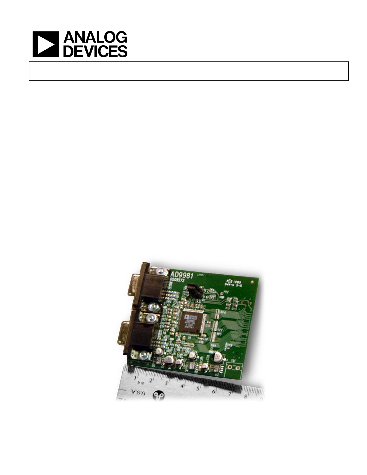
ANALOG FLAT PANEL INTERFACE BOARD
AD9981/PCB
PRODUCT DESCRIPTION
The purpose of the AD9981 evaluation board is both to
demonstrate the performance of the AD9981 and to serve as an
implementation example for design and layout. To aid in realworld evaluation, it was designed so that it could be connected
as easily as possible into another PC board, such as a graphics
controller board.
This board is for IC device evaluation purposes only. Analog
Devices does not recommend using this hardware outside of
this stated usage. Further, Analog Devices provides no warranties for use of this equipment beyond the scope of IC device
evaluation purposes.
REQUIREMENTS
The requirements to use the AD9981 evaluation board are a 5 V
power supply, graphics signals (through either of the 15-pin VGA
connectors), and a means to program the internal chip registers.
Hardware and software for programming the internal chip register are provided.
Rev. 0
Information furnished by Analog Devices is believed to be accurate and reliable.
However, no responsibility is assumed by Analog Devices for its use, nor for any
infringements of patents or other rights of third parties that may result from its use.
Specifications subject to change without notice. No license is granted by implication
or otherwise under any patent or patent rights of Analog Devices. Trademarks and
registered trademarks are the property of their respective owners.
Figure 1. Board Shown in Centimeters
05440-001
One Technology Way, P.O. Box 9106, Norwood, MA 02062-9106, U.S.A.
Tel: 781.329.4700
Fax: 781.461.3113 © 2005 Analog Devices, Inc. All rights reserved.
www.analog.com
Page 2

AD9981/PCB
TABLE OF CONTENTS
Evaluation Board Hardware ............................................................ 3
Sample Settings for The Evaluation Board ................................6
Typical Configuration.................................................................. 3
Power .............................................................................................. 3
Programming the Internal Chip Registers................................ 3
Evaluation Board Software .............................................................. 4
Settting up the Software............................................................... 4
AD9981 Software Control........................................................... 5
REVISION HISTORY
3/05—Revision 0: Initial Version
Schematics and Layout .....................................................................7
Ordering Information.................................................................... 11
Bill of Materials........................................................................... 11
Ordering Guide .......................................................................... 11
Contact Information.................................................................. 11
ESD Caution................................................................................ 11
Rev. 0 | Page 2 of 12
Page 3

AD9981/PCB
EVALUATION BOARD HARDWARE
TYPICAL CONFIGURATION
In most cases, this evaluation board is used to digitize analog
RGB graphics signals and pass the data to another board. To do
this, connect the graphics signals to the 15-pin VGA connector,
supply 5 V to the board, and program the internal serial
register. The digitized data, generated clock signals, and control
signals are passed off the board through the right-side
connector.
POWER
The AD9981 evaluation board contains two 3.3 V voltage
regulators and an adjustable regulator set for 1.8 V. These
regulators supply power to the AD9981. The three regulators
provide power to the three power supplies on the AD9981 (refer
to the AD9981 data sheet). The best performance can be
obtained from the AD9981 when the analog supply (V
) and
D
the PLL (PV
the primary 3.3 V supply (V
nominally when supplied with 5 V, but work with a range of
voltages. Power is applied to the board through the right-side
connector (Pins 1–4 of J3). Typically, power is supplied from
another board. In the AD9981 evaluation kit, 5 V is supplied by
the 10-bit display interface board.
PROGRAMMING THE INTERNAL CHIP REGISTERS
Hardware and software for programming the AD9981 internal
registers are provided. The hardware consists of a standard
printer cable and a receiver chip located on the panel driver
board. The programming signals come onto the AD9981
evaluation board through Pins 7 and 9 on Connector J3. The
software is included on the installation CD and is described in
the Evaluation Board Software section.
) supply have their own regulators separate from
D
). The three regulators work
DD
Rev. 0 | Page 3 of 12
Page 4
AD9981/PCB
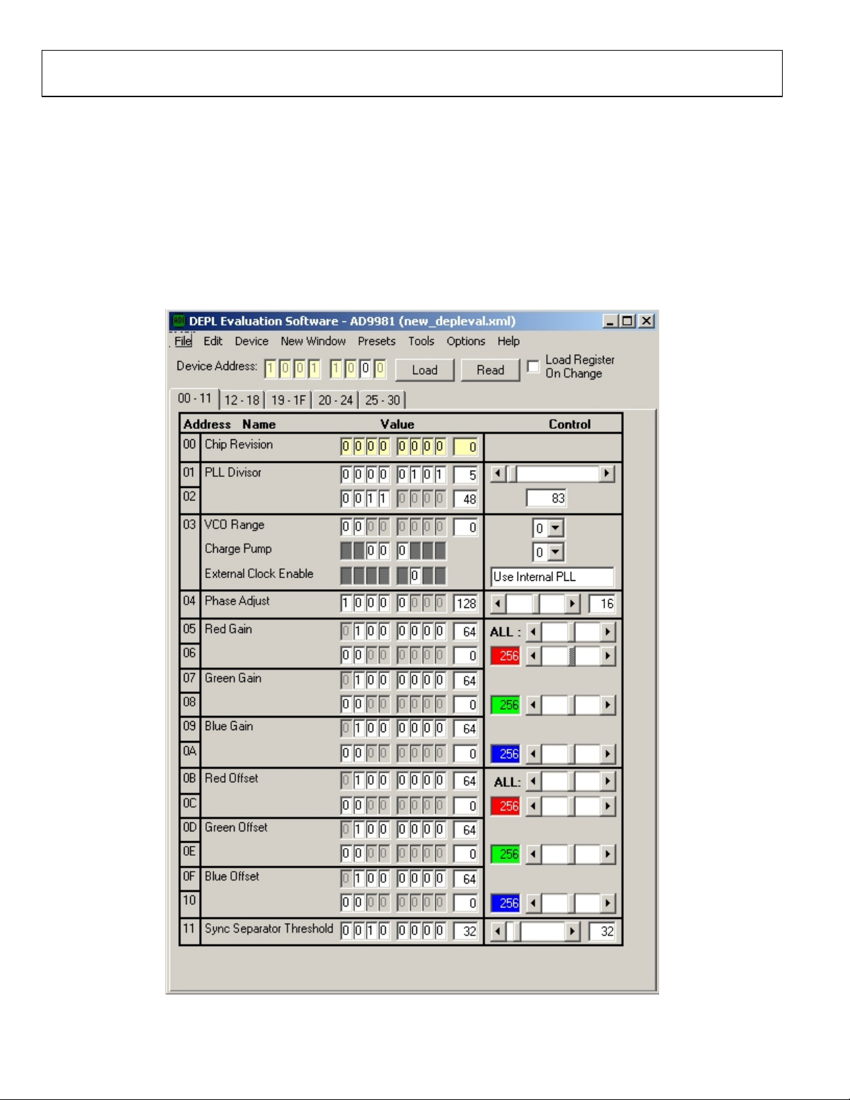
EVALUATION BOARD SOFTWARE
SETTTING UP THE SOFTWARE
The display electronics product line (DEPL) evaluation software
is a Visual Basic® program requiring Windows® 95, or later. It is
on a self-installing CD package included with the evaluation
board. When performing the software install, always use the
most recent Windows files (DLL or OCX, for example) if
prompted by the install software (these files may already be on
your system). The AD9882 register setup screen (similar to the
DEPL Evaluation Software – AD9981 register setup window in
Figure 2) should be displayed at program execution after a
successful installation. The DEPL evaluation software can
control any of the DEPL AD988x or AD998x devices. It can also
read and write to the 10-bit display interface board and includes
useful tools such as a PLL Divisor calculator.
Figure 2. DEPL Evaluation Software—AD9981 Register Setup Window
Rev. 0 | Page 4 of 12
Page 5

AD9981/PCB
AD9981 SOFTWARE CONTROL
To select the AD9981 as the target device for the DEPL
evaluation software, select Device > AD9981. This displays the
DEPL Evaluation Software – AD9981 register setup window,
as shown in Figure 2. From this window you can control every
bit within the AD9981. A detailed, bit-by-bit functional
description is provided in the AD9981 data sheet.
To update the registers in the AD9981, click Load at the top of
the window. This is true unless Load Register On Change is
checked. In this case, the appropriate register is updated as soon
as any change is made in the window. The five tabs in this
control window enable you to display groups of registers. The
selections are 00-011, 12-18, 19-24, or 25-30. Click the
appropriate tab to view/control the register desired.
PLL Settings
The PLL settings are in Registers 0x01 to 0x04. The PLL Divisor
setting (12 bits) can be set bit-by-bit (the value toggles when
clicking on the bit) by setting a value for Registers 0x01 and
0x02 (decimal value), by setting the 12-bit value (decimal
value), or by moving the control bar left (to decrease) or right
(to increase). When changing the value using one of these
methods, the change is reflected in the other three. The values
are not written to the AD9981 until you click Load.
The VCO Range and Charge Pump settings in Register 0x03
can be set by individual bit, by register, or by pull-down menu
selection.
The 5-bit Phase Adjust in Register 0x04 can be altered in the
some manner as the PLL Divisor.
Table 1 contains example PLL register settings for various video
modes. For PLL settings not included here, an Excel spreadsheet
for calculating PLL settings can be accessed under the Design
Tools section of the Analog Devices Display Electronics web site
at www.analog.com/flatpanel.
Gain and Offset Settings
The 9-bit gain control for the red, green, and blue video
channels are contained in Registers 0x05 to 0x0A and can be
changed bit-by-bit, by setting a value for the registers (decimal
value), or by moving the control bar left (to decrease) or right
(to increase). The 9-bit offset control for the red, green, and
blue channels are contained in Registers 0x0B to 0x10. These
can be set in the same manner as gain. Note that using the gain
and offset control bars at the top of their respective sections
changes all three channels by the same amount, regardless of
their setting. In other words, if, in order to achieve color
balance, your offset settings are 60, 70, and 80 for R, G, and B,
respectively, the minimum settings are 0, 10, and 20. The
maximum offset settings would then be 107, 117, and 127. To
control the gain or offset of an individual channel, separate
control bars for each color are also provided.
Sync Separator Control
Register 0x11 contains bits for setting the Sync Separator
Threshold. The threshold can be changed bit-by-bit by setting a
value for the register (decimal value), or by moving the control
bar left (to decrease) or right (to increase). The resulting state of
the register is reflected in the box to the right.
Sync Control
Registers 0x12 to 0x15 contain bits for controlling input and
output Hsync and Vsync signals. You can toggle each bit by
clicking on it. The resulting state of the bit is reflected in the
box to the right of each bit. The HSOUT and VSOUT (if
enabled) pulse widths can also be adjusted using the control bar
to the right of their respective registers.
Coast and Clamp Control
Pre-Coast, Post-Coast, various Coast and Clamp controls, and
Clamp Placement and Duration are controlled via Registers
0x16 to 0x1B. You can toggle each bit by clicking on it. The
resulting state of the bit is reflected in the box to the right of
each bit. The pre- and post-Coast as well as the Clamp
Placement and Duration registers can also be controlled via the
sliding bar to the right of their respective registers.
Auto-Offset Control
Register 0x1B contains bits for controlling the auto-offset
function. You can toggle each bit by clicking on it. The resulting
state of the bit is reflected in the box to the right of each bit. For
more details on this function, the application note
“Implementing the Auto-Offset Function of the AD9981” can
be downloaded from our web site. This information can also be
found in the AD9981 data sheet.
SOG Control and Power Management
Registers 0x1D and 0x1E contain bits for controlling the SOG,
Input Selection,m and Power Management functions. You can
toggle each bit by clicking on it. The resulting state of the bit is
reflected in the box to the right of each bit.
Output Control
Registers 0x1 and 0x20 contain bits for controlling Output
functions. You can toggle each bit by clicking on it. The
resulting state of the bit is reflected in the box to the right of
each bit. The Output Mode bits also have pull-down menus that
can be used for output mode selection.
Sync Pulse Filter Control
Registers 0x21 to 0x23 contain the bits for controlling Sync
Pulse Filter. These controls can be modified bit by bit, by
changing the 8-bit (decimal) value or by using the slider bar
to the right of each register.
Rev. 0 | Page 5 of 12
Page 6

AD9981/PCB
PLL Divider
VCO
1
Range
(0x03 7:6)
Charge Pump
Current
1
(0x03 5:3)
Latch Select
(0x2D 4:3)
Status Registers (Read-Only)
Registers 0x24 to 0x27 are read-only registers that provide
status for Hsync, Vsync, and SOG Detection (0x24), Hsync,
Vsync, Coast, and Clamp Polarity (0x25), and the Hsync per
Vsync Counter (0x16 to 0x27). Performing a read (by clicking
Read) lets you see the status of each of these bits. The status is
also reflected in the text to the right of each of these bits.
SAMPLE SETTINGS FOR THE EVALUATION BOARD
Table 1. Sample Settings
PLL Settings ADC Setting
Nominal
Mode Resolution
Frequency Hs (kHz)
VGA 640 × 480 at 60 Hz 31.469 25.175 800 00 101 01
640 × 480 at 72 Hz 37.861 31.500 832 01 011 01
640 × 480 at 75 Hz 37.500 31.500 840 01 011 01
640 × 480 at 85 Hz 43.269 36.000 832 01 100 01
SVGA 800 × 600 at 56 Hz 35.156 36.000 1024 01 100 01
800 × 600 at 60 Hz 37.879 40.000 1056 01 100 01
800 × 600 at 72 Hz 48.077 50.000 1040 01 110 01
800 × 600 at 75 Hz 46.875 49.500 1056 01 110 01
800 × 600 @ at 85 Hz 53.674 56.250 1048 01 110 01
XGA 1024 × 768 at 60 Hz 48.363 65.000 1344 10 100 01
1024 × 768 at 70 Hz 56.476 75.000 1328 10 100 01
1024 × 768 at 75 Hz 60.023 78.750 1312 10 101 01
1024 × 768 at 80 Hz 64.000 85.500 1336 10 101 01
1024 × 768 at 85 Hz 68.677 94.50 1376 10 110 01
SXGA 1280 × 1024 at 60 Hz 60.020 108.000 1688 10 111 10
TV 480i 15.750 13.510 858 00 001 01
480p 31.470 27.000 858 00 100 01
720p 45.000 74.250 1650 10 100 01
1080i 33.750 74.250 2200 10 100 01
1080p @30 Hz 33.750 74.250 2200 10 100 01
1
The VCO Range and Charge Pump Current settings are preliminary and may need slight adjustments.
Nominal Pixel
Clock (MHz)
Rev. 0 | Page 6 of 12
Page 7

AD9981/PCB
]
SCHEMATICS AND LAYOUT
SCL
SDA
COAST
VSYNC1
HSYNC1
VSYNC0
HSYNC0
CLAMP
Ω
R17
1k
22
11
Ω
R14
1k
66
67
68
69
70
71
72
73
78
SDA
SCL
FILT
BLUE_DATA_A[0:9]
[63:54]
BLUE[0:9]
HSYNC1
VSYNC1
HSYNC0
VSYNC0
CLAMP
EXTCLK/COAST
U1
AD9981
GND; 3, 7, 11, 15, 27, 39,
GREEN_DATA_A[0:9
[51:42]
GREEN[0:9]
VD; 1, 5, 9, 13
PVD; 41, 74, 76, 79
40, 53, 65, 75, 77, 80
OVDD; 26, 38, 52, 64
RED[0:9]
DATACK
25
SOGOUT
24
HSOUT
23
VSOUT/A0
22
O/EFIELD
21
[37:28]
TP9
TP8
TP7
TP6
TP5
RED_DATA_A[0:9]
1
1
1
1
1
DATA_CLOCK
SOG_OUT
HS_OUT
VS_OUT
PWRDN
ODD_EVEN~
2
R1
1.5kΩ
2
1
0.08µF
W2
2
131
HSYNC0
HSYNC0
HSYNC
HSYNC1
C25
W1
VSYNC0
2
C24
PVD
NOTE:
LABEL ALL TEST POINTS WITH
THE APPROPRIATE NET NAME.
VSYNC0
TP2
1
1
TP1
15151414131312121111101099887766554433221
J2
BIN0
0.008µF
C16
VSYNC
3
VSYNC1
CON-HD-15HFCON-HD-15HF
BAIN0
4
BIN1
C22
47nF
47nF
C15
BLU0
2
1
FB3
2
FB6
BV0
6
GIN0
RED0
GRN0
1
GV0
RV0
8
SOGIN0
C21
47nF
2
1
FB5
10
GIN1
1nF
C13
R5
221
221
R6
221
R7
12
SOGIN1
C20
47nF
75Ω
75Ω
75Ω
TP4
TP3
J1
14
RIN0
1nF
C19
20
19
18
17
16
RIN1
REFCM
REFLO
REFHI
C14
47nF
C18
0.1µF
C8
HSYNC1
C23
0.1µF
0.1µF
R8
1kΩ
2
1
BLU1
2
1
FB2
BV1
47nF
VSYNC1
1
1
RED1
GRN1
FB4
2
1
GV1
RV1
1
R11
10kΩ
12
R2
75Ω
R3
75Ω
R4
2
75Ω
1
FB1
1
1
1
05440-002
REFHI
REFCM
REFLO
PWRDN/TRI-ST
RAIN1
RAIN0
SOGIN1
GAIN1
SOGIN0
GAIN0
BAIN1
Figure 3.
Rev. 0 | Page 7 of 12
Page 8

AD9981/PCB
G
]
BLUE_DATA_A0
BLUE_DATA_A1
BLUE_DATA_A[0:9]
REEN_DATA_A[0:9
RED_DATA_A[0:9]
BLUE_DATA_A2
BLUE_DATA_A3
BLUE_DATA_A4
BLUE_DATA_A5
BLUE_DATA_A6
BLUE_DATA_A7
BLUE_DATA_A8
BLUE_DATA_A9
GREEN_DATA_A0
GREEN_DATA_A1
GREEN_DATA_A2
GREEN_DATA_A3
GREEN_DATA_A4
GREEN_DATA_A5
GREEN_DATA_A6
GREEN_DATA_A7
GREEN_DATA_A8
GREEN_DATA_A9
RED_DATA_A0
RED_DATA_A1
RED_DATA_A2
RED_DATA_A3
RP4
1
2
3
4
5
6
7
8
22
RP2
1
2
3
4
5
6
7
8
22
RP5
1
2
3
4
5
6
7
8
22
BLUE_OUT_A0
16
BLUE_OUT_A1
15
BLUE_OUT_A2
14
BLUE_OUT_A3
13
BLUE_OUT_A4
12
BLUE_OUT_A5
11
BLUE_OUT_A6
10
BLUE_OUT_A7
9
BLUE_OUT_A8
16
BLUE_OUT_A9
15
GREEN_OUT_A0
14
GREEN_OUT_A1
13
GREEN_OUT_A2
12
GREEN_OUT_A3
11
GREEN_OUT_A4
10
GREEN_OUT_A5
9
GREEN_OUT_A6
16
GREEN_OUT_A7
15
GREEN_OUT_A8
14
GREEN_OUT_A9
13
RED_OUT_A0
12
RED_OUT_A1
11
RED_OUT_A2
10
RED_OUT_A3
9
RED_DATA_A4
RED_DATA_A5
RED_DATA_A6
RED_DATA_A7
RED_DATA_A8
RED_DATA_A9
SOG_OUT
HS_OUT
VS_OUT
Figure 4.
RP1
1
2
3
4
5
6
7
8
22
RA7
22
RED_OUT_A4
16
RED_OUT_A5
15
RED_OUT_A6
14
RED_OUT_A7
13
RED_OUT_A8
12
RED_OUT_A9
11
10
9
DATA_CLOCK_OUTDATA_CLOCK
SOG
HSYNC_OUT
VSYNC_OUT
05440-003
Rev. 0 | Page 8 of 12
Page 9

AD9981/PCB
CTL3
CTL1
PWRDN
VSYNC
HSYNC
CLOCK_INVERT
DATA_CLOCK_OUT
CLAMP
NC
COAST
NC
GND
NC
NC
NC
NC
NC
NC
NC
NC
NC
NC
GND
NC
NC
NC
NC
NC
NC
NC
NC
NC
NC
GND
NC
NC
NC
NC
NC
NC
NC
NC
NC
NC
GND
NC
NC
GNDGND
VCC
2468101214161820222426283032343638404244464850525456586062646668707274767880828486889092949698
13579
NOTE: PINS 5, 6, 11, 12, 91, 92, AND 94 ARE NOT DEFINED.
VD
0.1µF
C2 C3
0.1µF
0.1µF
C4
C6
0.1µF
C27
+
1
NC
3
U2
ADP3303-3V3
NC
17
6
NR
ERR
OUTIN
82
111315171921232527293133353739414345474951535557596163656769717375777981838587899193959799
NC
NC
GND
SCL
SDA
BLUE_OUT_A5
BLUE_OUT_A4
BLUE_OUT_A3
BLUE_OUT_A2
BLUE_OUT_A1
BLUE_OUT_A0
22µF
2
NC
3
4
SD GND
5
U3
ADP3303-3V3
GND
BLUE_OUT_A9
BLUE_OUT_A8
BLUE_OUT_A7
BLUE_OUT_A6
OVDD
C11 C12
C9
C10
17
NR
OUTIN
82
0.1µF
0.1µF
0.1µF
0.1µF
NC
GREEN_OUT_A2
GREEN_OUT_A1
GREEN_OUT_A0
C28
22µF
+
1
2
6
ERR
4
SD GND
5
GREEN_OUT_A5
GREEN_OUT_A4
GREEN_OUT_A3
GND
RED_OUT_A5
RED_OUT_A4
RED_OUT_A3
RED_OUT_A2
RED_OUT_A1
RED_OUT_A0
GREEN_OUT_A9
GREEN_OUT_A8
GREEN_OUT_A7
GREEN_OUT_A6
PVD
C30 C31
C26
C17
1.8V
R9
1
5
64
OUT
U4
ADP3334
IN
3
GND
RED_OUT_A9
RED_OUT_A8
RED_OUT_A7
RED_OUT_A6
0.1µF
0.1µF
0.1µF
0.1µF
C29
22µF
+
2
1
76.8kΩ
R10
147kΩ
2
2
1
7
FB
1
SD GND
2
DATA_CLOCK_OUT
SOG
HSYNC_OUT
ODD_EVEN~
VSYNC_OUT
NC
DIG_DE
TB1
CTL0
VCC
1
X
100
CTL2
2
J3
MOLEX_53553-100
1
PR3
1
PR2
1
PR1
1
PR4
X
+
1
2
C1
47µF
VCC
+
1
2
C5
47µF
VCC
+
1
2
C7
22µF
VCC
05440-004
Figure 5.
Rev. 0 | Page 9 of 12
Page 10

AD9981/PCB
Figure 6.
Figure 7.
05440-005
05440-006
05440-007
Figure 8.
05440-008
Figure 9.
Rev. 0 | Page 10 of 12
Page 11
AD9981/PCB
ORDERING INFORMATION
BILL OF MATERIALS
Table 2.
L/I QTY REFDES Description Part No. Mfgr. Dist. Dist. Part No. Sub?
1 2 C1, C5 47 µF,16 V, ALUM, ELECTRO, 'D' ECE-V1CA470SP PANASONIC DIGIKEY PCE3164CT-ND Y
2 15 C2–C4, C6, C8–C12,
C17–C18, C23, C26,
C30–C31
3 4 C7, C27–C29 22 µF, 6.3 V, ALUM, ELECTRO ECE-V0JA220SR PANASONIC DIGIKEY PCE3056CT-ND Y
4 6 C13–C16, C19, C22 .047 µF, 50 V, X7R, 0805, CER ECJ-2YB1H473K PANASONIC DIGIKEY PCC1836CT-ND Y
5 2 C20, C21 .001 µF, 50 V, NPO, 0805, CER ECU-V1H102KBN PANASONIC DIGIKEY PCC102BNCT-ND Y
6 1 C24 .082 µF, 50 V, X7R, 0805, CER ECJ-2YB1H823K PANASONIC DIGIKEY PCC1839CT-ND Y
7 1 C25 8200 pF, 50 V, X7R, 0805, CER ECU-V1H822KBG PANASONIC DIGIKEY PCC822BNCT-ND Y
8 6 FB1–FB6 120 Ω @100 MHz BEAD, 0805 2508051217Z0 FAIR-RITE ALLIED 589-0585 N
9 2 J1, J2 15-PIN D-SUB CONN 181-015-212-171 NORCOMP DIGIKEY 815RF-ND N
10 1 J3 100-PIN MATED CONNECTOR 53553-1009 MOLEX FORCE 53553-1009 N
11 1 R1 1.50 kΩ, 1%, 1/10W 0805 ERJ-6ENF1501V PANASONIC DIGIKEY P1.50KCCT-ND Y
12 6 R2–R7 75.0 Ω, 1%, 1/10W 0805 ERJ-6ENF75R0V PANASONIC DIGIKEY P75.0CCT-ND Y
13 3 R8, R14, R17 1.00 kΩ, 1%, 1/10W 0805 ERJ-6ENF1001V PANASONIC DIGIKEY P1.00KCCT-ND Y
14 1 R9 76.8 kΩ, 1%, 1/10W 0805 ERJ-6ENF7682V PANASONIC DIGIKEY P76.8KCCT-ND Y
15 1 R10 147 kΩ, 1%, 1/10W 0805 ERJ-6ENF1472V PANASONIC DIGIKEY P147KCCT-ND Y
16 2 R18, R19 150 Ω, 1%, 1/10W 0805 ERJ-6ENF1500V PANASONIC DIGIKEY P150CCT-ND Y
17 2 R20, R21 2.00 kΩ, 1%, 1/10W 0805 ERJ-6ENF2001V PANASONIC DIGIKEY P2.00KCCT-ND Y
18 1 RA7 22 Ω RPAK, 1/16W, 5%, 4RES 742C083220J CTS DIGIKEY 742C083220JCT-ND Y
19 4 RP1, RP2, RP4, RP5 22 Ω RPAK, 1/16W, 5%, 8RES 742C163220J CTS DIGIKEY 742C163220JCT-ND Y
20 1 TB1 NOT POPULATED
21 1 U1 IC,10-BIT CONVERTER AD9981 ADI ADI AD9981 N
22 2 U2, U3 IC, 3.3 V REGULATOR ADP3303AR-3.3 ADI ADI ADP3303AR-3.3 N
23 1 U4 IC, VAR REGULATOR ADP3334 ADI ADI ADP3334 N
24 1 N/A PC BOARD GSO8272 ADI PCSM GSO8272 N
25 4 N/A SCREW 4-40 X 3/8" FOR J1, J2 SPC NEWARK 31G2198 Y
26 4 N/A 4-40 HEX NUT FOR J1, J2 SPC NEWARK 31F2106 Y
27 2 W1, W2 3-PIN HEADER 2340-6111TN 3M MOUSER 2340-6111TN Y
.1 µF, 25 V, X7R, 0805, CER ECJ-2VB1E104K PANASONIC DIGIKEY PCC1828CT-ND Y
ORDERING GUIDE
Model Package Description
AD9981/PCB Evaluation Board
CONTACT INFORMATION
Questions? Please email us directly at flatpanel_apps@analog.com, visit our web site at http://www.analog.com/flatpanel, or call the
Analog Devices help line at 1-800-AnalogD.
ESD CAUTION
ESD (electrostatic discharge) sensitive device. Electrostatic charges as high as 4000 V re adily accumulate on
the human body and test equipment and can discharge without detection. Although this product features
proprietary ESD protection circuitry, permanent damage may occur on devices subjected to high energy
electrostatic discharges. Therefore, proper ESD precautions are recommended to avoid performance degradation or loss of functionality.
Rev. 0 | Page 11 of 12
Page 12

AD9981/PCB
NOTES
© 2005 Analog Devices, Inc. All rights reserved. Trademarks and
registered trademarks are the property of their respective owners.
EB05440–0–3/05(0)
Rev. 0 | Page 12 of 12
 Loading...