

Page 1
10-Bit CCD Signal Processor with
FEATURES
Correlated Double Sampler (CDS)
0 dB to 18 dB Pixel Gain Amplifier (
PxGA
®
)
6 dB to 42 dB 10-Bit Variable Gain Amplifier (VGA)
10-Bit 25 MSPS A/D Converter
Black Level Clamp with Variable Level Control
Complete On-Chip Timing Driver
Precision Timing Core with 800 ps Resolution
On-Chip 3 V Horizontal and RG Drivers
40-Lead LFCSP Package
APPLICATIONS
Digital Still Cameras
High Speed Digital Imaging Applications
Precision Timing
™
Core
AD9948
GENERAL DESCRIPTION
The AD9948 is a highly integrated CCD signal processor for
digital still camera applications. Specified at pixel rates of up to
25 MHz, the AD9948 consists of a complete analog front end
with A/D conversion, combined with a programmable timing
driver. The Precision Timing core allows adjustment of high
speed clocks with 800 ps resolution.
The analog front end includes black level clamping, CDS, PxGA,
VGA, and a 25 MHz 10-bit A/D converter. The timing driver
provides the high speed CCD clock drivers for RG and H1–H4.
Operation is programmed using a 3-wire serial interface.
Packaged in a space-saving 40-lead LFCSP package, the
AD9948 is specified over an operating temperature range of
–20°C to +85°C.
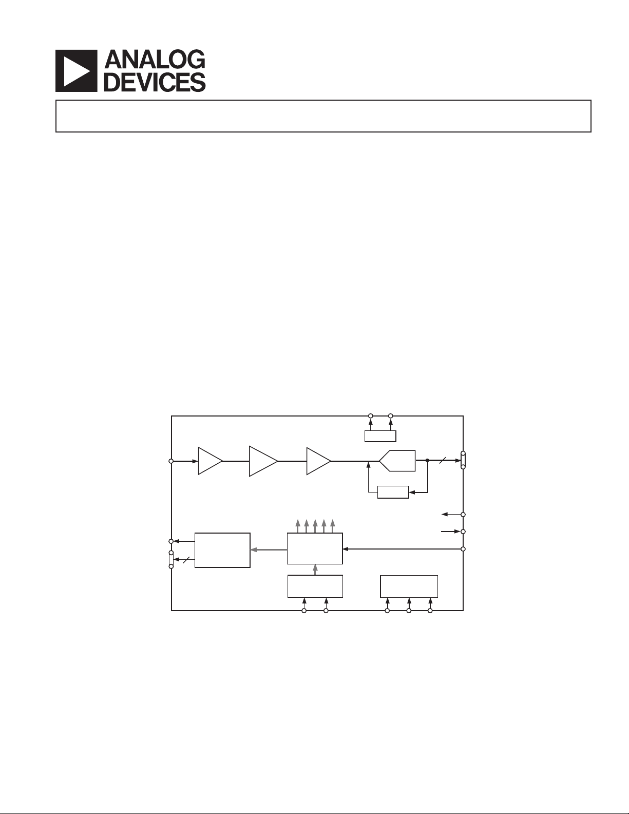
CCDIN
RG
H1–H4
4
AD9948
CDS
HORIZONTAL
DRIVERS
FUNCTIONAL BLOCK DIAGRAM
REFB
REFT
V
0dB TO 18dB
PxGA
6dB TO 42dB
VGA
INTERNAL
CLOCKS
PRECISION
TIMING
CORE
SYNC
GENERATOR
HD VD
REF
CLAMP
SL
10-BIT
ADC
INTERNAL
REGISTERS
10
DOUT
HBLK
CLP/PBLK
CLI
SDATASCK
REV. 0
Information furnished by Analog Devices is believed to be accurate and
reliable. However, no responsibility is assumed by Analog Devices for its
use, nor for any infringements of patents or other rights of third parties that
may result from its use. No license is granted by implication or otherwise
under any patent or patent rights of Analog Devices. Trademarks and
registered trademarks are the property of their respective companies.
One Technology Way, P.O. Box 9106, Norwood, MA 02062-9106, U.S.A.
Tel: 781/329-4700 www.analog.com
Fax: 781/326-8703 © 2003 Analog Devices, Inc. All rights reserved.
Page 2
AD9948–SPECIFICATIONS
GENERAL SPECIFICATIONS
Parameter Min Typ Max Unit
TEMPERATURE RANGE
Operating –20 +85 °C
Storage –65 +150 °C
MAXIMUM CLOCK RATE 25 MHz
POWER SUPPLY VOLTAGE
AVDD, TCVDD (AFE, Timing Core) 2.7 3.0 3.6 V
HVDD (H1–H4 Drivers) 2.7 3.0 3.6 V
RGVDD (RG Driver) 2.7 3.0 3.6 V
DRVDD (D0–D9 Drivers) 2.7 3.0 3.6 V
DVDD (All Other Digital) 2.7 3.0 3.6 V
POWER DISSIPATION
25 MHz, HVDD = RGVDD = 3 V, 100 pF H1–H4 Loading* 220 mW
Total Shutdown Mode 1 mW
*The total power dissipated by the HVDD supply may be approximated using the equation
Total HVDD Power C HVDD Pixel Frequency HVDD Number of H Outputs Used
Reducing the H-loading, using only two of the outputs, and/or using a lower HVDD supply will reduce the power dissipation.
Specifications subject to change without notice.
=×× ×× −()()
LOAD
DIGITAL SPECIFICATIONS
(T
to T
MIN
, AVDD = DVDD = DRVDD = HVDD = RGVDD = 2.7 V, CL = 20 pF, unless otherwise noted.)
MAX
Parameter Symbol Min Typ Max Unit
LOGIC INPUTS
High Level Input Voltage V
Low Level Input Voltage V
High Level Input Current I
Low Level Input Current I
Input Capacitance C
IH
IL
IH
IL
IN
2.1 V
0.6 V
10 µA
10 µA
10 pF
LOGIC OUTPUTS
High Level Output Voltage, IOH = 2 mA V
Low Level Output Voltage, IOL = 2 mA V
OH
OL
2.2 V
0.5 V
CLI INPUT
High Level Input Voltage
(TCVDD/2 + 0.5 V) V
Low Level Input Voltage V
IH–CLI
IL–CLI
1.85 V
0.85 V
RG AND H-DRIVER OUTPUTS
High Level Output Voltage
(RGVDD – 0.5 V and HVDD – 0.5 V) V
Low Level Output Voltage V
OH
OL
2.2 V
0.5 V
Maximum Output Current (Programmable) 30 mA
Maximum Load Capacitance 100 pF
Specifications subject to change without notice.
REV. 0–2–
Page 3
AD9948
(T
to T
, AVDD = DVDD = 3.0 V, f
MAX
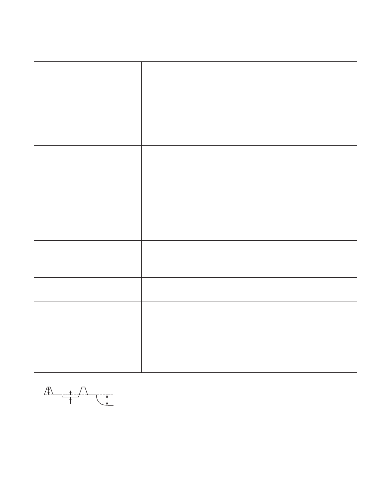
ANALOG SPECIFICATIONS
MIN
unless otherwise noted.)
Parameter Min Typ Max Unit Notes
CDS
Gain 0 dB
Allowable CCD Reset Transient* 500 mV
Max Input Range before Saturation* 1.0 V p-p
Max CCD Black Pixel Amplitude* ±50 mV
PIXEL GAIN AMPLIFIER (PxGA)
Gain Control Resolution 256 Steps
Gain Monotonicity
Min Gain 0 dB
Max Gain 18 dB
VARIABLE GAIN AMPLIFIER (VGA)
Max Input Range 1.0 V p-p
Max Output Range 2.0 V p-p
Gain Control Resolution 1024 Steps
Gain Monotonicity Guaranteed
Gain Range
Min Gain (VGA Code 0) 6 dB
Max Gain (VGA Code 1023) 42 dB
BLACK LEVEL CLAMP
Clamp Level Resolution 256 Steps
Clamp Level Measured at ADC output
Min Clamp Level (0) 0 LSB
Max Clamp Level (255) 63.75 LSB
A/D CONVERTER
Resolution 10 Bits
Differential Nonlinearity (DNL) –1.0 ± 0.5 +1.0 LSB
No Missing Codes Guaranteed
Full-Scale Input Voltage 2.0 V
VOLTAGE REFERENCE
Reference Top Voltage (REFT) 2.0 V
Reference Bottom Voltage (REFB) 1.0 V
SYSTEM PERFORMANCE Specifications include entire
VGA Gain Accuracy
Min Gain (Code 0) 5.0 5.5 6.0 dB
Max Gain (Code 1023) 40.5 41.5 42.5 dB
Peak Nonlinearity, 500 mV Input Signal 0.2 % 12 dB gain applied
Total Output Noise 0.25 LSB rms AC grounded input, 6 dB
Power Supply Rejection (PSR) 50 dB Measured with step change
*Input signal characteristics defined as follows:
= 25 MHz, Typical Timing Specifications,
CLI
signal chain
gain applied
on supply
500mV TYP
RESET TRANSIENT
Specifications subject to change without notice.
50mV MAX
OPTICAL BLACK PIXEL
1V MAX
INPUT SIGNAL RANGE
REV. 0
–3–
Page 4
AD9948
TIMING SPECIFICATIONS
(CL = 20 pF, f
= 25 MHz, Serial Timing in Figure 3, unless otherwise noted.)
CLI
Parameter Symbol Min Typ Max Unit
MASTER CLOCK (CLI) (See Figure 4)
CLI Clock Period t
CLI High/Low Pulsewidth t
CLI
ADC
40 ns
16 20 24 ns
Delay from CLI to Internal Pixel
Period Position t
CLPOB Pulsewidth (Programmable)* t
CLIDLY
COB
220 Pixels
6ns
SAMPLE CLOCKS (See Figure 6)
SHP Rising Edge to SHD Rising Edge t
S1
17 20 ns
DATA OUTPUTS (See Figures 7a and 7b)
Output Delay From Programmed Edge t
OD
6ns
Pipeline Delay 11 Cycles
SERIAL INTERFACE
Maximum SCK Frequency f
SL to SCK Setup Time t
SCK to SL Hold Time t
SDATA Valid to SCK Rising Edge Setup t
SCK Falling Edge to SDATA Valid Hold t
SCK Falling Edge to SDATA Valid Read t
*Minimum CLPOB pulsewidth is for functional operation only. Wider typical pulses are recommended to achieve low noise clamp reference.
Specifications subject to change without notice.
SCLK
LS
LH
DS
DH
DV
10 MHz
10 ns
10 ns
10 ns
10 ns
10 ns
ABSOLUTE MAXIMUM RATINGS*
With
Parameter Respect To Min Max Unit
AVDD, TCVDD AVSS –0.3 +3.9 V
HVDD, RGVDD HVSS, RGVSS –0.3 +3.9 V
DVDD, DRVDD DVSS, DRVSS –0.3 +3.9 V
Any VSS Any VSS –0.3 +0.3 V
Digital Outputs DRVSS –0.3 DRVDD + 0.3 V
CLPOB/PBLK, HBLK DVSS –0.3 DVDD + 0.3 V
SCK, SL, SDATA DVSS –0.3 DVDD + 0.3 V
RG RGVSS –0.3 RGVDD + 0.3 V
H1–H4 HVSS –0.3 HVDD + 0.3 V
REFT, REFB, CCDIN AVSS –0.3 AVDD + 0.3 V
Junction Temperature 150 °C
Lead Temperature (10 sec) 300 °C
*Stresses above those listed under Absolute Maximum Ratings may cause permanent damage to the device. This is a stress
rating only; functional operation of the device at these or any other conditions above those listed in the operational sections
of this specification is not implied. Exposure to absolute maximum rating conditions for extended periods may affect
device reliability.
ORDERING GUIDE
Temperature Package Package
Model Range Description Option
AD9948KCP –20°C to +85°C LFCSP CP-40
AD9948KCPRL –20°C to +85°C LFCSP CP-40
THERMAL CHARACTERISTICS
Thermal Resistance
40-Lead LFCSP Package
= 27°C/W*
JA
*
is measured using a 4-layer PCB with the exposed paddle
JA
soldered to the board.
AD9948KCPZ* –20°C to +85°C LFCSP CP-40
AD9948KCPZRL* –20°C to +85°C LFCSP CP-40
*This is a lead free product.
CAUTION
ESD (electrostatic discharge) sensitive device. Electrostatic charges as high as 4000 V readily
accumulate on the human body and test equipment and can discharge without detection. Although
the AD9948 features proprietary ESD protection circuitry, permanent damage may occur on
devices subjected to high energy electrostatic discharges. Therefore, proper ESD precautions are
recommended to avoid performance degradation or loss of functionality.
REV. 0–4–
Page 5
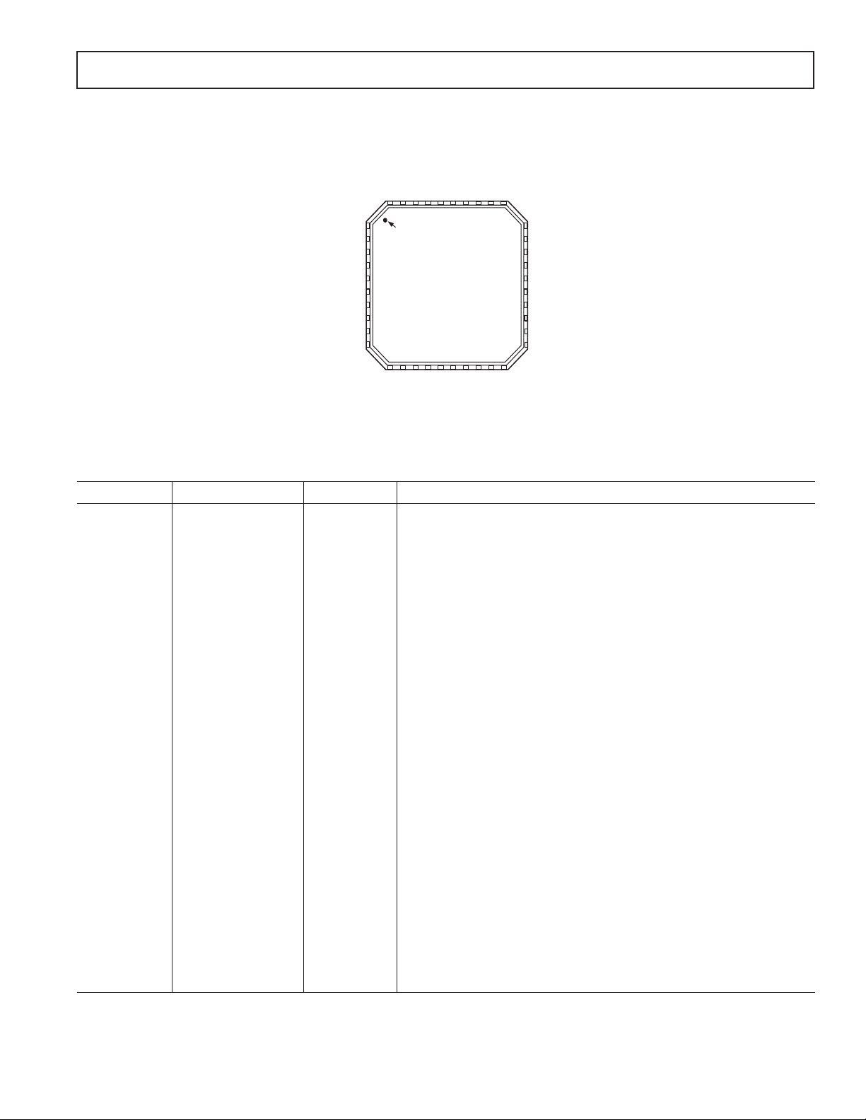
PIN CONFIGURATION
40 NC
38 HBLK
37 DVDD
36 DVSS
35 HD
34 VD
32 SDI
39 CLP/PBLK
33 SCK
31 SL
AD9948
NC 1
(LSB) D0 2
D1 3
D2 4
DRVSS 5
DRVDD 6
D3 7
D4 8
D5 9
D6 10
PIN 1
IDENTIFIER
D7 11
D8 12
AD9948
TOP VIEW
H1 14
H2 15
HVSS 16
(MSB) D9 13
H3 18
HVDD 17
30 REFB
29 REFT
28 AVSS
27 CCDIN
26 AVDD
25 CLI
24 TCVDD
23 TCVSS
22 RGVDD
21 RG
H4 19
RGVSS 20
PIN FUNCTION DESCRIPTIONS
Pin No. Mnemonic Type* Description
2–4 D0–D2 DO Data Outputs (D0 is LSB)
5 DRVSS P Digital Driver Ground
6 DRVDD P Digital Driver Supply
7–13 D3–D9 DO Data Outputs (D9 is MSB)
14 H1 DO CCD Horizontal Clock 1
15 H2 DO CCD Horizontal Clock 2
16 HVSS P H1–H4 Driver Ground
17 HVDD P H1–H4 Driver Supply
18 H3 DO CCD Horizontal Clock 3
19 H4 DO CCD Horizontal Clock 4
20 RGVSS P RG Driver Ground
21 RG DO CCD Reset Gate Clock
22 RGVDD P RG Driver Supply
23 TCVSS P Analog Ground for Timing Core
24 TCVDD P Analog Supply for Timing Core
25 CLI DI Master Clock Input
26 AVDD P Analog Supply for AFE
27 CCDIN AI Analog Input for CCD Signal (Connect through Series 0.1 µF Capacitor)
28 AVSS P Analog Ground for AFE
29 REFT AO Reference Top Decoupling (Decouple with 1.0 µF to AVSS)
30 REFB AO Reference Bottom Decoupling (Decouple with 1.0 µF to AVSS)
31 SL DI 3-Wire Serial Load
32 SDI DI 3-Wire Serial Data Input
33 SCK DI 3-Wire Serial Clock
34 VD DI Vertical Sync Pulse
35 HD DI Horizontal Sync Pulse
36 DVSS P Digital Ground
37 DVDD P Digital Supply
38 HBLK DI Optional HBLK Input
39 CLP/PBLK DO CLPOB or PBLK Output
1, 40 NC Not Internally Connected
*Type: AI = Analog Input, AO = Analog Output, DI = Digital Input, DO = Digital Output, P = Power.
REV. 0
–5–
Page 6
AD9948
TERMINOLOGY
Differential Nonlinearity (DNL)
An ideal ADC exhibits code transitions that are exactly 1 LSB
apart. DNL is the deviation from this ideal value. Thus every
code must have a finite width. No missing codes guaranteed to
10-bit resolution indicates that all 1024 codes, respectively,
must be present over all operating conditions.
Peak Nonlinearity
Peak nonlinearity, a full signal chain specification, refers to the
peak deviation of the output of the AD9948 from a true straight
line. The point used as zero scale occurs 0.5 LSB before the
first code transition. Positive full scale is defined as a level 1 LSB
and 0.5 LSB beyond the last code transition. The deviation is
measured from the middle of each particular output code to the
true straight line. The error is then expressed as a percentage of
the 2 V ADC full-scale signal. The input signal is always appropriately gained up to fill the ADC’s full-scale range.
EQUIVALENT CIRCUITS
AVDD
R
Total Output Noise
The rms output noise is measured using histogram techniques.
The standard deviation of the ADC output codes is calculated in
LSB, and represents the rms noise level of the total signal chain
at the specified gain setting. The output noise can be converted
to an equivalent voltage, using the relationship
12
LSB (ADC full scale/ codes)=
n
where n is the bit resolution of the ADC. For the AD9948,
1LSB is approximately 1.95 mV.
Power Supply Rejection (PSR)
The PSR is measured with a step change applied to the supply
pins. The PSR specification is calculated from the change in the
data outputs for a given step change in the supply voltage.
DVD D
330
AVSS
AVSS
Circuit 1. CCDIN (Pin 27)
AVDD
330
CLI
25k
1.4V
AVSS
Circuit 2. CLI (Pin 25)
DVSS DRVDD
DATA
THREE-
STATE
DVSS DRVSS
Circuit 3. Data Outputs D0–D9 (Pins 2–4, 7–13)
DOUT
DVSS
Circuit 4. Digital Inputs (Pins 31–35, 38)
HVDD or RGVDD
DATA
ENABLE
HVSS or RGVSS
Circuit 5. H1–H4 and RG (Pins 14, 15, 18, 19, 21)
OUTPUT
REV. 0–6–
Page 7
1.0
0.5
0
DNL (LSB)
–0.5
Typical Performance Characteristics–AD9948
–1.0
0
200 600 800
400
ADC OUTPUT CODE
TPC 1. Typical DNL
10
7.5
5.0
OUTPUT NOISE (LSB)
2.5
0
0
200
400
VGA GAIN CODE (LSB)
600 800
TPC 2. Output Noise vs. VGA Gain
275
1000
1000
REV. 0
250
225
200
175
150
POWER DISSIPATION (mW)
125
100
10
VDD = 3.3V
VDD = 3.0V
VDD = 2.7V
15
SAMPLE RATE (MHz)
20
TPC 3. Power Curves
25
–7–
Page 8
AD9948
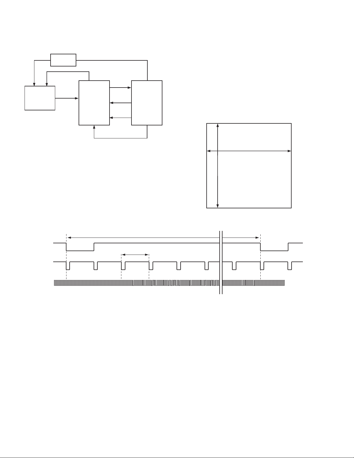
SYSTEM OVERVIEW
V-DRIVER
V1–Vx, VSG1–VSGx, SUBCK
H1–H4, RG
DOUT
CCD
CCDIN
INTEGRATED
SERIAL
INTERFACE
AD9948
AFE + TD
HD, VD
CLI
DIGITAL IMAGE
PROCESSING
ASIC
Figure 1. Typical Application
Figure 1 shows the typical system application diagram for the
AD9948. The CCD output is processed by the AD9948’s AFE
circuitry, which consists of a CDS, a PxGA, a VGA, a black level
clamp, and an A/D converter. The digitized pixel information is
sent to the digital image processor chip, where all postprocessing
and compression occurs. To operate the CCD, CCD timing
parameters are programmed into the AD9948 from the image
processor through the 3-wire serial interface. From the system
master clock, CLI, provided by the image processor, the AD9948
generates the high speed CCD clocks and all internal AFE clocks.
All AD9948 clocks are synchronized with VD and HD. All of
the AD9948’s horizontal pulses (CLPOB, PBLK, and HBLK)
are programmed and generated internally.
The H-drivers for H1–H4 and RG are included in the AD9948,
allowing these clocks to be connected directly to the CCD.
H-drive voltage of 3 V is supported in the AD9948.
Figure 2a shows the horizontal and vertical counter dimensions
for the AD9948. All internal horizontal clocking is programmed
using these dimensions to specify line and pixel locations.
MAXIMUM FIELD DIMENSIONS
12-BIT HORIZONTAL = 4096 PIXELS MAX
12-BIT VERTICAL = 4096 LINES MAX
Figure 2a. Vertical and Horizontal Counters
VD
HD
CLI
MAX VD LENGTH IS 4095 LINES
MAX HD LENGTH IS 4095 PIXELS
Figure 2b. Maximum VD/HD Dimensions
REV. 0–8–
Page 9
AD9948
SERIAL INTERFACE TIMING
All of the internal registers of the AD9948 are accessed through
a 3-wire serial interface. Each register consists of an 8-bit address
and a 24-bit data-word. Both the 8-bit address and 24-bit dataword are written starting with the LSB. To write to each register,
a 32-bit operation is required, as shown in Figure 3a. Although
many registers are less than 24 bits wide, all 24 bits must be
written for each register. If the register is only 16 bits wide, then
the upper eight bits are don’t cares and may be filled with zeros
during the serial write operation. If fewer than 24 bits are written,
the register will not be updated with new data.
Figure 3b shows a more efficient way to write to the registers by
using the AD9948’s address auto-increment capability. Using
this method, the lowest desired address is written first, followed
by multiple 24-bit data-words. Each new 24-bit data-word will
be written automatically to the next highest register address. By
eliminating the need to write each 8-bit address, faster register
loading is achieved. Address auto-increment may be used starting with any register location, and may be used to write to as
few as two registers or as many as the entire register space.
8-BIT ADDRESS
COMPLETE REGISTER LISTING
All addresses and default values are expressed in hexadecimal.
All registers are VD/HD updated as shown in Figure 3a, except
for the registers indicated in Table I, which are SL updated.
Table I. SL-Updated Registers
Register Description
OPRMODE AFE Operation Modes
CTLMODE AFE Control Modes
SW_RESET Software Reset Bit
TGCORE _RSTB Reset Bar Signal for Internal TG Core
PREVENTUPDATE Prevents Update of Registers
VDHDEDGE VD/HD Active Edge
FIELDVAL Resets Internal Field Pulse
HBLKRETIME Retimes the HBLK to Internal Clock
CLPBLKOUT CLP/BLK Output Pin Select
CLPBLKEN Enables CLP/BLK Output Pin
H1CONTROL H1/H2 Polarity Control
RGCONTROL H1 Positive Edge Location
DRVCONTROL H1 Negative Edge Location
SAMPCONTROL H1 Drive Current
DOUTPHASE H2 Drive Current
24-BIT DATA
SDATA
SCK
SDATA
SCK
A0 A1 A2 A4 A5 A6 A7
t
DS
1 32234567891011 12 30 31
t
LS
SL
VD
HD
NOTES
1. INDIVIDUAL SDATA BITS ARE LATCHED ON SCK RISING EDGES.
2. ALL 32 BITS MUST BE WRITTEN: 8 BITS FOR ADDRESS AND 24 BITS FOR DATA.
3. IF THE REGISTER LENGTH IS <24 BITS, THEN DON’T CARE BITS MUST BE USED TO COMPLETE THE 24-BIT DATA LENGTH.
4. NEW DATA IS UPDATED AT EITHER THE SL RISING EDGE OR AT THE HD FALLING EDGE AFTER THE NEXT VD FALLING EDGE.
5. VD/HD UPDATE POSITION MAY BE DELAYED TO ANY HD FALLING EDGE IN THE FIELD USING THE UPDATE REGISTER.
A3
t
DH
D1 D2 D3 D21 D22 D23
D0
...
...
...
...
...
t
LH
SL UPDATED
Figure 3a. Serial Write Operation
DATA FOR STARTING
REGISTER ADDRESS
A0 A1 A2 A4 A5 A6 A7 D0 D1 D22 D23
1 322345678910 31
A3
...
...
DATA FOR NEXT
REGISTER ADDRESS
D0 D1 D22 D23
...
...
3433 5655
VD/HD UPDATED
D0
D2D1
585759
...
...
REV. 0
SL
NOTES
1. MULTIPLE SEQUENTIAL REGISTERS MAY BE LOADED CONTINUOUSLY.
2. THE FIRST (LOWEST ADDRESS) REGISTER ADDRESS IS WRITTEN, FOLLOWED BY MULTIPLE 24-BIT DATA-WORDS.
3. THE ADDRESS WILL AUTOMATICALLY INCREMENT WITH EACH 24-BIT DATA-WORD (ALL 24 BITS MUST BE WRITTEN).
4. SL IS HELD LOW UNTIL THE LAST DESIRED REGISTER HAS BEEN LOADED.
5. NEW DATA IS UPDATED AT EITHER THE SL RISING EDGE OR AT THE HD FALLING EDGE AFTER THE NEXT VD FALLING EDGE.
...
...
Figure 3b. Continuous Serial Write Operation
–9–
...
Page 10

AD9948
Table II. AFE Register Map
Data Bit Default
Address Content Value Name Description
00 [11:0] 4 OPRMODE AFE Operation Modes. (See Table VIII.)
01 [9:0] 0 VGAGAIN VGA Gain.
02 [7:0] 80 CLAMP LEVEL Optical Black Clamp Level.
03 [11:0] 4 CTLMODE AFE Control Modes. (See Table IX.)
04 [17:0] 0 PxGA GAIN01 PxGA Gain Registers for Color 0 [8:0] and Color 1 [17:9].
05 [17:0] 0 PxGA GAIN23 PxGA Gain Registers for Color 2 [8:0] and Color 3 [17:9].
Table III. Miscellaneous Register Map
Data Bit Default
Address Content Value Name Description
10 [0] 0 SW_RST Software Reset.
1 = Reset all registers to default, then self-clear back to 0.
11 [0] 0 OUT_CONTROL Output Control.
0 = Make all dc outputs inactive.
12 [0] 0 TGCORE_RSTB Timing Core Reset Bar.
0 = Reset TG core.
1 = Resume operation.
13 [11:0] 0 UPDATE Serial Update.
Sets the line (HD) within the field to update serial data.
14 [0] 0 PREVENTUPDATE Prevents the update of the VD-Updated Registers.
1 = Prevent update.
15 [0] 0 VDHDEDGE VD/HD Active Edge.
0 = Falling edge triggered.
1 = Rising edge triggered.
16 [1:0] 0 FIELDVAL Field Value Sync.
0 = Next Field 0.
1 = Next Field 1.
2/3 = Next Field 2.
17 [0] 0 HBLKRETIME Retime HBLK to Internal H1 Clock.
Preferred setting is 1. Setting to 1 will add one cycle delay to HBLK
toggle positions.
18 [1:0] 0 CLPBLKOUT CLP/BLK Pin Output Select.
0 = CLPOB.
1 = PBLK.
2 = HBLK.
3 = Low.
19 [0] 1 CLPBLKEN Enable CLP/BLK Output.
1 = Enable.
1A [0] 0 TEST MODE Internal Test Mode.
Should always be set low.
REV. 0–10–
Page 11

AD9948
Table IV. CLPOB Register Map
Data Bit Default
Address Content Value (Hex) Name Description
20 [3:0] F CLPOBPOL Start Polarities for CLPOB Sequences 0, 1, 2, and 3.
21 [23:0] FFFFFF CLPOBTOG_0 Sequence 0. Toggle Position 1 [11:0] and Toggle Position 2 [23:12].
22 [23:0] FFFFFF CLPOBTOG_1 Sequence 1. Toggle Position 1 [11:0] and Toggle Position 2 [23:12].
23 [23:0] FFFFFF CLPOBTOG_2 Sequence 2. Toggle Position 1 [11:0] and Toggle Position 2 [23:12].
24 [23:0] FFFFFF CLPOBTOG_3 Sequence 3. Toggle Position 1 [11:0] and Toggle Position 2 [23:12].
0 CLPOBSCP0 CLPOB Sequence-Change-Position 0 (Hard-Coded to 0).
25 [7:0] 0 CLPOBSPTR CLPOB Sequence Pointers for Region 0 [1:0], 1 [3:2], 2 [5:4], 3 [7:6].
26 [11:0] FFF CLPOBSCP1 CLPOB Sequence-Change-Position 1.
27 [11:0] FFF CLPOBSCP2 CLPOB Sequence-Change-Position 2.
28 [11:0] FFF CLPOBSCP3 CLPOB Sequence-Change-Position 3.
Table V. PBLK Register Map
Data Bit Default
Address Content Value (Hex) Name Description
30 [3:0] F PBLKPOL Start Polarities for PBLK Sequences 0, 1, 2, and 3.
31 [23:0] FFFFFF PBLKTOG_0 Sequence 0. Toggle Position 1 [11:0] and Toggle Position 2 [23:12].
32 [23:0] FFFFFF PBLKTOG_1 Sequence 1. Toggle Position 1 [11:0] and Toggle Position 2 [23:12].
33 [23:0] FFFFFF PBLKTOG_2 Sequence 2. Toggle Position 1 [11:0] and Toggle Position 2 [23:12].
34 [23:0] FFFFFF PBLKTOG_3 Sequence 3. Toggle Position 1 [11:0] and Toggle Position 2 [23:12].
0 PBLKSCP0 PBLK Sequence-Change-Position 0 (Hard-Coded to 0).
35 [7:0] 0 PBLKSPTR PBLK Sequence Pointers for Region 0 [1:0], 1 [3:2], 2 [5:4], 3 [7:6].
36 [11:0] FFF PBLKSCP1 PBLK Sequence-Change-Position 1.
37 [11:0] FFF PBLKSCP2 PBLK Sequence-Change-Position 2.
38 [11:0] FFF PBLKSCP3 PBLK Sequence-Change-Position 3.
REV. 0
–11–
Page 12

AD9948
Table VI. HBLK Register Map
Data Bit Default
Address Content Value (Hex) Name Description
40 [0] 0 HBLKDIR HBLK Internal/External.
0 = Internal.
1 = External.
41 [0] 0 HBLKPOL HBLK External Active Polarity.
0 = Active Low.
1 = Active High.
42 [0] 1 HBLKEXTMASK HBLK External Masking Polarity.
0 = Mask H1 Low.
1 = Mask H1High.
43 [3:0] F HBLKMASK HBLK Internal Masking Polarity.
0 = Mask H1 Low.
1 = Mask H1 High.
44 [23:0] FFFFFF HBLKTOG12_0 Sequence 0. Toggle Position 1 [11:0] and Toggle Position 2 [23:12].
45 [23:0] FFFFFF HBLKTOG34_0 Sequence 0. Toggle Position 3 [11:0] and Toggle Position 4 [23:12].
46 [23:0] FFFFFF HBLKTOG56_0 Sequence 0. Toggle Position 5 [11:0] and Toggle Position 6 [23:12].
47 [23:0] FFFFFF HBLKTOG12_1 Sequence 1. Toggle Position 1 [11:0] and Toggle Position 2 [23:12].
48 [23:0] FFFFFF HBLKTOG34_1 Sequence 1. Toggle Position 3 [11:0] and Toggle Position 4 [23:12].
49 [23:0] FFFFFF HBLKTOG56_1 Sequence 1. Toggle Position 5 [11:0] and Toggle Position 6 [23:12].
4A [23:0] FFFFFF HBLKTOG12_2 Sequence 2. Toggle Position 1 [11:0] and Toggle Position 2 [23:12].
4B [23:0] FFFFFF HBLKTOG34_2 Sequence 2. Toggle Position 3 [11:0] and Toggle Position 4 [23:12].
4C [23:0] FFFFFF HBLKTOG56_2 Sequence 2. Toggle Position 5 [11:0] and Toggle Position 6 [23:12].
4D [23:0] FFFFFF HBLKTOG12_3 Sequence 3. Toggle Position 1 [11:0] and Toggle Position 2 [23:12].
4E [23:0] FFFFFF HBLKTOG34_3 Sequence 3. Toggle Position 3 [11:0] and Toggle Position 4 [23:12].
4F [23:0] FFFFFF HBLKTOG56_3 Sequence 3. Toggle Position 5 [11:0] and Toggle Position 6 [23:12].
0 HBLKSCP0 HBLK Sequence-Change-Position 0 (Hard-coded to 0).
50 [7:0] 0 HBLKSPTR HBLK Sequence Pointers for Region 0 [1:0], 1 [3:2], 2 [5:4], 3 [7:6].
51 [11:0] FFF HBLKSCP1 HBLK Sequence-Change-Position 1.
52 [11:0] FFF HBLKSCP2 HBLK Sequence-Change-Position 2.
53 [11:0] FFF HBLKSCP3 HBLK Sequence-Change-Position 3.
Table VII. H1–H2, RG, SHP, SHD Register Map
Data Bit Default
Address Content Value Name Description
60 [12:0] 01001 H1CONTROL H1 Signal Control. Polarity [0] (0 = Inversion, 1 = No Inversion).
H1 Positive Edge Location [6:1].
H1 Negative Edge Location [12:7].
61 [12:0] 00801 RGCONTROL RG Signal Control. Polarity [0] (0 = Inversion, 1 = No Inversion).
RG Positive Edge Location [6:1].
RG Negative Edge Location [12:7].
62 [14:0] 0 DRVCONTROL Drive Strength Control for H1 [2:0], H2 [5:3], H3 [8:6], H4 [11:9], and
RG [14:12].
Drive Current Values: 0 = Off, 1 = 4.3 mA, 2 = 8.6 mA, 3 = 12.9 mA,
4 = 17.2 mA, 5 = 21.5 mA, 6 = 25.8 mA, 7 = 30.1 mA.
63 [11:0] 00024 SAMPCONTROL SHP/SHD Sample Control. SHP Sampling Location [5:0].
SHD Sampling Location [11:6].
64 [5:0] 0 DOUTPHASE DOUT Phase Control.
REV. 0–12–
Page 13

Table VIII. AFE Operation Register Detail
Data Bit Default
Address Content Value Name Description
00 [1:0] 0 PWRDOWN 0 = Normal Operation.
1 = Reference Standby.
2/3 = Total Power-Down.
[2] 1 CLPENABLE 0 = Disable OB Clamp.
1 = Enable OB Clamp.
[3] 0 CLPSPEED 0 = Select Normal OB Clamp Settling.
1 = Select Fast OB Clamp Settling.
[4] 0 FASTUPDATE 0 = Ignore VGA Update.
1 = Very Fast Clamping when VGA Is Updated.
[5] 0 PBLK_LVL DOUT Value during PBLK.
0 = Blank to Zero.
1 = Blank to Clamp Level.
[7:6] 0 TEST MODE Test Operation Only. Set to zero.
[8] 0 DCBYP 0 = Enable DC Restore Circuit.
1 = Bypass DC Restore Circuit during PBLK.
[9] 0 TESTMODE Test Operation Only. Set to zero.
[11:10] 0 CDSGAIN Adjustment of CDS Gain.
0 = 0 dB.
01= –2 dB.
10 = –4 dB.
11 = 0 dB.
AD9948
Table IX. AFE Control Register Detail
Data Bit Default
Address Content Value Name Description
04 [1:0] 0 COLORSTEER 0 = Off.
1 = Progressive.
2 = Interlaced.
3 = Three Field.
[2] 1 PXGAENABLE 0 = Disable PxGA.
1 = Enable PxGA.
[3] 0 DOUTDISABLE 0 = Data Outputs Are Driven.
1 = Data Outputs Are Three-Stated.
[4] 0 DOUTLATCH 0 = Latch Data Outputs with DOUT Phase.
1 = Output Latch Transparent.
[5] 0 GRAYENCODE 0 = Binary Encode Data Outputs.
1= Gray Encode Data Outputs.
REV. 0
–13–
Page 14
AD9948
PRECISION TIMING HIGH SPEED TIMING GENERATION
The AD9948 generates flexible high speed timing signals using
the Precision Timing core. This core is the foundation for generating the timing used for both the CCD and the AFE; the reset
gate RG, horizontal drivers H1–H4, and the SHP/SHD sample
clocks. A unique architecture makes it routine for the system
designer to optimize image quality by providing precise control
over the horizontal CCD readout and the AFE correlated
double sampling.
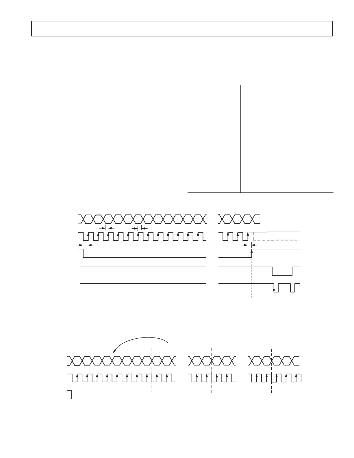
Timing Resolution
The Precision Timing core uses a 1× master clock input (CLI)
as a reference. This clock should be the same as the CCD pixel
clock frequency. Figure 4 illustrates how the internal timing core
divides the master clock period into 48 steps or edge positions.
Therefore, the edge resolution of the Precision Timing core is
/48). For more information on using the CLI input, refer to
(t
CLI
the Applications Information section.
POSITION
CLI
1 PIXEL
PERIOD
t
CLIDLY
P[0] P[48] = P[0]
P[12] P[24] P[36]
...
High Speed Clock Programmability
Figure 5 shows how the high speed clocks, RG, H1–H4, SHP,
and SHD, are generated. The RG pulse has programmable rising
and falling edges, and may be inverted using the polarity control.
The horizontal clocks H1 and H3 have programmable rising and
falling edges, and polarity control. The H2 and H4 clocks are
always inverses of H1 and H3, respectively. Table X summarizes
the high speed timing registers and their parameters.
Each edge location setting is 6 bits wide, but only 48 valid edge
locations are available. Therefore, the register values are mapped
into four quadrants, with each quadrant containing 12 edge
locations. Table XI shows the correct register values for the
corresponding edge locations.
...
NOTES
1. PIXEL CLOCK PERIOD IS DIVIDED INTO 48 POSITIONS, PROVIDING FINE EDGE RESOLUTION FOR HIGH SPEED CLOCKS.
2. THERE IS A FIXED DELAY FROM THE CLI INPUT TO THE INTERNAL PIXEL PERIOD POSITIONS (
t
CLIDLY
= 6 ns TYP).
Figure 4. High Speed Clock Resolution From CLI Master Clock Input
(3)
CCD SIGNAL
RG
H1/H3
H2/H4
(1) (2)
(5) (6)
PROGRAMMABLE CLOCK POSITIONS:
1. RG RISING EDGE
2. RG FALLING EDGE
3. SHP SAMPLE LOCATION
4. SHD SAMPLE LOCATION
5. H1/H3 RISING EDGE POSITION
6. H1/H3 FALLING EDGE POSITION (H2/H4 ARE INVERSE OF H1/H3)
(4)
Figure 5. High Speed Clock Programmable Locations
Table X. H1CONTROL, RGCONTROL, DRVCONTROL, and SAMPCONTROL Register Parameters
Parameter Length Range Description
Polarity 1b High/Low Polarity Control for H1/H3 and RG (0 = No Inversion, 1 = Inversion).
Positive Edge 6b 0–47 Edge Location Positive Edge Location for H1/H3 and RG.
Negative Edge 6b 0–47 Edge Location Negative Edge Location for H1/H3 and RG.
Sample Location 6b 0–47 Sample Location Sampling Location for SHP and SHD.
Drive Control 3b 0–7 Current Steps Drive Current for H1–H4 and RG Outputs, 0–7 Steps of 4.1 mA Each.
DOUT Phase 6b 0–47 Edge Location Phase Location of Data Outputs with Respect to Pixel Period.
REV. 0–14–
Page 15

AD9948
Table XI. Precision Timing Edge Locations
Quadrant Edge Location (Decimal) Register Value (Decimal) Register Value (Binary)
I0 to 11 0 to 11 000000 to 001011
II 12 to 23 16 to 27 010000 to 011011
III 24 to 35 32 to 43 100000 to 101011
IV 36 to 47 48 to 59 110000 to 111011
H-Driver and RG Outputs
In addition to the programmable timing positions, the AD9948
features on-chip output drivers for the RG and H1–H4 outputs.
These drivers are powerful enough to directly drive the CCD
inputs. The H-driver and RG driver current can be adjusted
for optimum rise/fall time into a particular load by using the
DRVCONTROL register (Address x062). The DRVCONTROL
register is divided into five different 3-bit values, each one being
adjustable in 4.1 mA increments. The minimum setting of 0 is
equal to OFF or three-state, and the maximum setting of 7 is
equal to 30.1 mA.
t
H1/H3
H2/H4
RISE
<<
tPDt
RISE
FIXED CROSSOVER VOLTAGE
Figure 6. H-Clock Inverse Phase Relationship
As shown in Figure 6, the H2/H4 outputs are inverses of H1/H3.
The internal propagation delay resulting from the signal inversion
is less than l ns, which is significantly less than the typical rise
time driving the CCD load. This results in a H1/H2 crossover
voltage at approximately 50% of the output swing. The crossover
voltage is not programmable.
Digital Data Outputs
The AD9948 data output phase is programmable using the
DOUTPHASE register (Address x064). Any edge from 0 to 47
may be programmed, as shown in Figure 7a. The pipeline delay
for the digital data output is shown in Figure 7b.
t
PD
H1/H3 H2/H4
REV. 0
CLI
CCDIN
SHD
(INTERNAL)
DOUT
1 PIXEL PERIOD
CLI
DOUT
P[0]
t
OD
NOTES
1. DIGITAL OUTPUT DATA (DOUT) PHASE IS ADJUSTABLE WITH RESPECT TO THE PIXEL PERIOD.
2. WITHIN ONE CLOCK PERIOD, THE DATA TRANSITION CAN BE PROGRAMMED TO ANY OF THE 48 LOCATIONS.
P[12]
P[24]
P[36]
P[48] = P[0]
Figure 7a. Digital Output Phase Adjustment
t
CLIDLY
N–1
N–13
NOTES
DEFAULT TIMING VALUES ARE SHOWN: SHDLOC = 0, DOUT PHASE = 0.
HIGHER VALUES OF SHD AND/OR DOUTPHASE WILL SHIFT DOUT TRANSITION TO THE RIGHT, WITH RESPECT TO CLI LOCATION.
N N+1
SAMPLE PIXEL N
N–12
N+2
N+3
PIPELINE LATENCY = 11 CYCLES
N+12N+11N+10N+9N+8N+7N+6N+5N+4
N–3N–4N–5N–6N–7N–8N–9N–10N–11
N–2
N–1
N
Figure 7b. Pipeline Delay for Digital Data Output
–15–
N+13
N+1
Page 16

AD9948
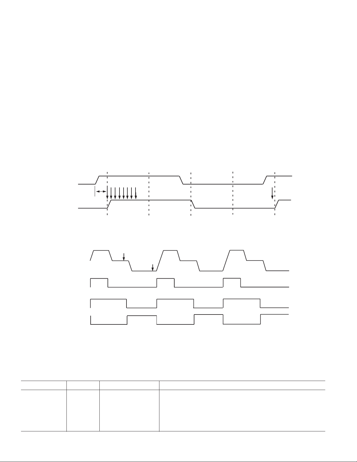
HORIZONTAL CLAMPING AND BLANKING
The AD9948’s horizontal clamping and blanking pulses are
fully programmable to suit a variety of applications. Individual
sequences are defined for each signal, which are then organized
into multiple regions during image readout. This allows the dark
pixel clamping and blanking patterns to be changed at each
stage of the readout to accommodate different image transfer
timing and high speed line shifts.
Individual CLPOB and PBLK Sequences
The AFE horizontal timing consists of CLPOB and PBLK, as
shown in Figure 8. These two signals are independently programmed using the parameters shown in Table XII. The start
polarity, first toggle position, and second toggle position are
HD
CLPOB
(1)
PBLK
PROGRAMMABLE SETTINGS:
1. START POLARITY (CLAMP AND BLANK REGION ARE ACTIVE LOW)
2. FIRST TOGGLE POSITION
3. SECOND TOGGLE POSITION
(3)(2)
ACTIVE
Figure 8. Clamp and Preblank Pulse Placement
fully programmable for each signal. The CLPOB and PBLK
signals are active low, and should be programmed accordingly.
Up to four individual sequences can be created for each signal.
Individual HBLK Sequences
The HBLK programmable timing shown in Figure 9 is similar
to CLPOB and PBLK. However, there is no start polarity control. Only the toggle positions are used to designate the start and
the stop positions of the blanking period. Additionally, there is a
polarity control, HBLKMASK, which designates the polarity of
the horizontal clock signals H1–H4 during the blanking period.
Setting HBLKMASK high will set H1 = H3 = low and H2 =
H4 = high during the blanking, as shown in Figure 10. Up to
four individual sequences are available for HBLK.
. . .
. . .
ACTIVE
. . .
HD
(1)
HBLK
PROGRAMMABLE SETTINGS:
1. FIRST TOGGLE POSITION = START OF BLANKING
2. SECOND TOGGLE POSITION = END OF BLANKING
Parameter Length Range Description
Polarity 1b High/Low Starting Polarity of Clamp and PBLK Pulses for Sequences 0–3.
Toggle Position 1 12b 0–4095 Pixel Location First Toggle Position within the Line for Sequences 0–3.
Toggle Position 2 12b 0–4095 Pixel Location Second Toggle Position within the Line for Sequences 0–3.
Parameter Length Range Description
HBLKMASK 1b High/Low Masking Polarity for H1 for Sequences 0–3 (0 = H1 Low, 1 = H1 High).
Toggle Position 1 12b 0–4095 Pixel Location First Toggle Position within the Line for Sequences 0–3.
Toggle Position 2 12b 0–4095 Pixel Location Second Toggle Position within the Line for Sequences 0–3.
Toggle Position 3 12b 0–4095 Pixel Location Third Toggle Position within the Line for Sequences 0–3.
Toggle Position 4 12b 0–4095 Pixel Location Fourth Toggle Position within the Line for Sequences 0–3.
Toggle Position 5 12b 0–4095 Pixel Location Fifth Toggle Position within the Line for Sequences 0–3.
Toggle Position 6 12b 0–4095 Pixel Location Sixth Toggle Position within the Line for Sequences 0–3.
(2)
BLANK
BLANK
Figure 9. Horizontal Blanking (HBLK) Pulse Placement
Table XII. CLPOB and PBLK Individual Sequence Parameters
Table XIII. HBLK Individual Sequence Parameters
. . .
REV. 0–16–
Page 17

HD
HBLK
H1/H3
AD9948
. . .
. . .
THE POLARITY OF H1 DURING BLANKING IS PROGRAMMABLE (H2 IS OPPOSITE POLARITY OF H1).
. . .
H1/H3
H2/H4
. . .
Figure 10. HBLK Masking Control
TOG1
HBLK
H1/H3
H2/H4
SPECIAL H-BLANK PATTERN IS CREATED USING MULTIPLE HBLK TOGGLE POSITIONS.
TOG2 TOG3
TOG4 TOG5 TOG6
Figure 11. Generating Special HBLK Patterns
Table XIV. Horizontal Sequence Control Parameters for CLPOB, PBLK, and HBLK
Register Length Range Description
SCP 12b 0–4095 Line Number CLOB/PBLK/HBLK SCP to Define Horizontal Regions 0–3.
SPTR 2b 0–3 Sequence Number Sequence Pointer for Horizontal Regions 0–3.
GENERATING SPECIAL HBLK PATTERNS
Six toggle positions are available for HBLK. Normally, only
two of the toggle positions are used to generate the standard
HBLK interval. However, the additional toggle positions may be
used to generate special HBLK patterns, as shown in Figure 11.
The pattern in this example uses all six toggle positions to
generate two extra groups of pulses during the HBLK interval. By changing the toggle positions, different patterns can
be created.
Horizontal Sequence Control
The AD9948 uses sequence change positions (SCPs) and sequence
pointers (SPTRs) to organize the individual horizontal sequences.
Up to four SCPs are available to divide the readout into four
separate regions, as shown in Figure 12. The SCP 0 is always hardcoded to Line 0, and SCP1–SCP3 are register programmable.
During each region bounded by the SCP, the SPTR registers
REV. 0
–17–
designate which sequence is used by each signal. CLPOB, PBLK,
and HBLK each have a separate set of SCPs. For example,
CLPOBSCP1 will define Region 0 for CLPOB, and in that region,
any of the four individual CLPOB sequences may be selected with
the CLPOBSPTR register. The next SCP defines a new region,
and in that region each signal can be assigned to a different
individual sequence. The sequence control registers are summarized in Table XIV.
External HBLK Signal
The AD9948 can also be used with an external HBLK signal. Setting the HBLKDIR register (Address x040) to high will disable the
internal HBLK signal generation. The polarity of the external
signal is specified using the HBLKPOL register, and the masking polarity of H1 is specified using the HBLKMASK register.
Table XV summarizes the register values when using an external
HBLK signal.
Page 18

AD9948
SEQUENCE CHANGE OF POSITION 0
SEQUENCE CHANGE OF POSITION 1
SEQUENCE CHANGE OF POSITION 2
SEQUENCE CHANGE OF POSITION 3
(V-COUNTER = 0)
UP TO FOUR INDIVIDUAL HORIZONTAL CLAMP AND BLANKING REGIONS MAY BE
PROGRAMMED WITHIN A SINGLE FIELD, USING THE SEQUENCE CHANGE POSITIONS.
SINGLE FIELD (1 VD INTERVAL)
CLAMP AND PBLK SEQUENCE REGION 0
CLAMP AND PBLK SEQUENCE REGION 1
CLAMP AND PBLK SEQUENCE REGION 2
CLAMP AND PBLK SEQUENCE REGION 3
Figure 12. Clamp and Blanking Sequence Flexibility
Table XV. External HBLK Register Parameters
Register Length Range Description
HBLKDIR 1b High/Low Specifies HBLK Internally Generated or Externally Supplied.
1 = External.
HBLKPOL 1b High/Low External HBLK Active Polarity.
0 = Active Low.
1 = Active High.
HBLKEXTMASK 1b High/Low External HBLK Masking Polarity.
0 = Mask H1 Low.
1 = Mask H1 High.
VD
H-COUNTER
(PIXEL COUNTER)
PxGA GAIN
REGISTER
HD
CLI
XXXXXXX
X
X
XXXXXXX
NOTES
1. INTERNAL H-COUNTER IS RESET SEVEN CLI CYCLES AFTER THE HD FALLING EDGE (WHEN USING VDHDEDGE = 0).
2. TYPICAL TIMING RELATIONSHIP: CLI RISING EDGE COINCIDES WITH HD FALLING EDGE.
3. PxGA STEERING IS SYNCHRONIZED WITH THE RESET OF THE INTERNAL H-COUNTER (MOSAIC SEPARATE MODE IS SHOWN).
H-COUNTER
RESET
X
01234567891011121415012 3
XXX
000 1 12111 0 031100
Figure 13. H-Counter Synchronization
H-COUNTER SYNCHRONIZATION
The H-Counter reset occurs seven CLI cycles following the HD
falling edge. The PxGA steering is synchronized with the reset
of the internal H-Counter (see Figure 13).
023
REV. 0–18–
Page 19

POWER-UP PROCEDURE
VDD
(INPUT)
CLI
(INPUT)
SERIAL
WRITES
VD
(OUTPUT)
HD
(OUTPUT)
DIGITAL
OUTPUTS
t
PWR
...
ODD FIELD EVEN FIELD
1 H
...
H2/H4
H1/H3, RG
CLOCKS ACTIVE WHEN OUT_CONTROL REGISTER IS
UPDATED AT VD/HD EDGE
Figure 14. Recommended Power-Up Sequence
AD9948
1V
...
...
Recommended Power-Up Sequence
When the AD9948 is powered up, the following sequence is
recommended (refer to Figure 14 for each step):
1. Turn on the power supplies for the AD9948.
2. Apply the master clock input, CLI, VD, and HD.
3. Although the AD9948 contains an on-chip power-on reset, a
software reset of the internal registers is recommended. Write
a 1 to the SW_RST register (Address x010), which will reset
all the internal registers to their default values. This bit is
self-clearing and will automatically be reset back to 0.
4. The Precision Timing core must be reset by writing a 0 to the
TGCORE_RSTB register (Address x012) followed by writing
a l to the TGCORE_RSTB register. This will start the internal
timing core operation.
5. Write a 1 to the PREVENTUPDATE register (Address x014).
This will prevent the updating of the serial register data.
6. Write to the desired registers to configure high speed timing
and horizontal timing.
7. Write a 1 to the OUT_CONTROL register (Address x011).
This will allow the outputs to become active after the next
VD/HD rising edge.
8. Write a 0 to the PREVENTUPDATE register (Address x014).
This will allow the serial information to be updated at next
VD/HD falling edge.
The next VD/HD falling edge allows register updates to occur,
including OUT_CONTROL, which enables all clock outputs.
REV. 0
–19–
Page 20

AD9948
1.0F
CCDIN
DC RESTORE
1.5V
SHP
0dB, –2dB, –4dB
CDS
SHD
SHP
PxGA GAIN
REGISTERS
SHD
0dB ~ 18dB
PxGA
DOUT
PHASE
CLPOB
6dB ~ 42dB
VGA
VGA GAIN
REGISTER
PBLK
DAC
1.0F 1.0F
1.0V 2.0V
INTERNAL
V
REF
10-BIT
ADC
OPTICAL BLACK
CLAMP
DIGITAL
FILTER
REFTREFB
2V FULL SCALE
CLAMP LEVEL
REGISTER
CLPOB
8
AD9948
OUTPUT
DATA
LATCH
PBLK
DOUT
PHASE
10
DOUT
PRECISION
TIMING
GENERATION
V- H
TIMING
GENERATION
Figure 15. Analog Front End Functional Block Diagram
ANALOG FRONT END DESCRIPTION AND OPERATION
The AD9948 signal processing chain is shown in Figure 15. Each
processing step is essential in achieving a high quality image from
the raw CCD pixel data.
DC Restore
To reduce the large dc offset of the CCD output signal,
adcrestore circuit is used with an external 0.1 µF series coupling capacitor. This restores the dc level of the CCD signal to
approximately 1.5 V to be compatible with the 3 V supply voltage
of the AD9948.
Correlated Double Sampler
The CDS circuit samples each CCD pixel twice to extract the
video information and reject low frequency noise. The timing
shown in Figure 5 illustrates how the two internally generated
CDS clocks, SHP and SHD, are used to sample the reference
level and the CCD signal level, respectively. The placement of
the SHP and SHD sampling edges is determined by the setting
of the SAMPCONTROL register located at Address 0x63.
Placement of these two clock signals is critical in achieving the
best performance from the CCD.
The gain in the CDS is fixed at 0 dB by default. Using Bits D10
and D11 in the AFE operation register, the gain may be reduced
to –2 dB or –4 dB. This will allow the AD9948 to accept an input
signal of greater than 1 V p-p. See Table VIII for register details.
PxGA
The PxGA provides separate gain adjustment for the individual
color pixels. A programmable gain amplifier with four separate
values, the PxGA has the capability to multiplex its gain value on
a pixel-to-pixel basis (see Figure 16). This allows lower output
color pixels to be gained up to match higher output color pixels.
Also, the PxGA may be used to adjust the colors for white balance, reducing the amount of digital processing that is needed.
The four different gain values are switched according to the color
steering circuitry. Three different color steering modes for different types of CCD color filter arrays are programmable in the AFE
CTLMODE register at Address 0x03 (see Figures 18a to 18c for
timing examples). For example, progressive steering mode accommodates the popular Bayer arrangement of red, green, and blue
filters (see Figure 17a).
VD
HD
SHP/SHD
8
COLOR
STEERING
CONTROL
2
4:1
MUX
PxGA STEERING
3
SELECTION
GAIN0
GAIN1
GAIN2
GAIN3
MODE
PxGA GAIN
REGISTERS
CONTROL
REGISTER
BITS D0–D1
Table XVI. Adjustable CDS Gain
Operation Register Bits
D11 D10 CDS Gain Max CDS Input
00 0 dB 1.0 V p-p
01 –2 dB 1.2 V p-p
10 –4 dB 1.6 V p-p
11 0 dB 1.0 V p-p
CDS
PxGA
VGA
Figure 16. PxGA Block Diagram
REV. 0–20–
Page 21

AD9948
CCD: PROGRESSIVE BAYER
RR
Gr
Gb B
RR
Gr
Gb B
Gr
Gb B
Gr
Gb B
COLOR STEERING MODE:
PROGRESSIVE
LINE0 GAIN0, GAIN1, GAIN0, GAIN1, ...
LINE1
LINE2
GAIN2, GAIN3, GAIN2, GAIN3, ...
GAIN0, GAIN1, GAIN0, GAIN1, ...
Figure 17a. CCD Color Filter Example—Progressive Scan
The same Bayer pattern can also be interlaced, and the interlaced
mode should be used with this type of CCD (see Figure 17b).
The color steering performs the proper multiplexing of the R,
G, and B gain values (loaded into the PxGA gain registers), and
is synchronized by the user with vertical (VD) and horizontal
(HD) sync pulses. For timing information, see Figure 18b.
CCD: INTERLACED BAYER
EVEN FIELD
RR
Gr
RR
Gr
RR
Gr
RR
Gr
ODD FIELD
Gb GbBB
Gb GbBB
Gb GbBB
Gr
Gr
Gr
Gr
COLOR STEERING MODE:
INTERLACED
LINE0 GAIN0, GAIN1, GAIN0, GAIN1, ...
LINE1
LINE2
LINE0 GAIN2, GAIN3, GAIN2, GAIN3, ...
LINE1
LINE2
GAIN0, GAIN1, GAIN0, GAIN1, ...
GAIN0, GAIN1, GAIN0, GAIN1, ...
GAIN2, GAIN3, GAIN2, GAIN3, ...
GAIN2, GAIN3, GAIN2, GAIN3, ...
A third type of readout uses the Bayer pattern divided into three
different readout fields. The three-field mode should be used
with this type of CCD (see Figure 17c). The color steering
performs the proper multiplexing of the R, G, and B gain values
(loaded into the PxGA gain registers), and is synchronized by
the user with vertical (VD) and horizontal (HD) sync pulses.
For timing information, see Figure 18c.
CCD: 3-FIELD READOUT
FIRST FIELD
RR
Gr
Gb GbBB
RR
Gr
Gb GbBB
SECOND FIELD
Gb GbBB
RR
Gr
Gb GbBB
RR
Gr
THIRD FIELD
RR
Gr
Gb GbBB
RR
Gr
Gb GbBB
Gr
Gr
Gr
Gr
Gr
Gr
COLOR STEERING MODE:
THREE FIELD
LINE0 GAIN0, GAIN1, GAIN0, GAIN1, ...
LINE1
LINE2
LINE0 GAIN2, GAIN3, GAIN2, GAIN3, ...
LINE1
LINE2
LINE0 GAIN0, GAIN1, GAIN0, GAIN1, ...
LINE1
LINE2
GAIN2, GAIN3, GAIN2, GAIN3, ...
GAIN0, GAIN1, GAIN0, GAIN1, ...
GAIN0, GAIN1, GAIN0, GAIN1, ...
GAIN2, GAIN3, GAIN2, GAIN3, ...
GAIN2, GAIN3, GAIN2, GAIN3, ...
GAIN0, GAIN1, GAIN0, GAIN1, ...
Gb GbBB
Figure 17b. CCD Color Filter Example—Interlaced Readout
Figure 17c. CCD Color Filter Example—Three-Field Readout
REV. 0
–21–
Page 22

AD9948
FIELDVAL
VD
HD
PxGA GAIN
REGISTER
NOTES
1. VD FALLING EDGE WILL RESET THE PxGA GAIN REGISTER STEERING TO 0101 LINE.
2. HD FALLING EDGES WILL ALTERNATE THE PxGA GAIN REGISTER STEERING BETWEEN 0101 AND 2323 LINES.
3. FIELDVAL IS ALWAYS RESET TO 0 ON VD FALLING EDGES.
FIELDVAL = 0
0
110XX
22033 11
022033 11
FIELDVAL = 0
0
110
Figure 18a. PxGA Color Steering—Progressive Mode
FIELDVAL
VD
HD
PxGA GAIN
REGISTER
NOTES
1. FIELDVAL = 0 (START OF FIRST FIELD) WILL RESET THE PxGA GAIN REGISTER STEERING TO 0101 LINE.
2. FIELDVAL = 1 (START OF SECOND FIELD) WILL RESET THE PxGA GAIN REGISTER STEERING TO 2323 LINE.
3. HD FALLING EDGES WILL RESET THE PxGA GAIN REGISTER STEERING TO EITHER 0 (FIELDVAL = 0) OR 2 (FIELDVAL = 1).
4. FIELDVAL WILL TOGGLE BETWEEN 0 AND 1 ON EACH VD FALLING EDGE.
FIELDVAL = 0
110XX
0
00 311 22
FIELDVAL = 1 FIELDVAL = 0
31100 00
2
332
Figure 18b. PxGA Color Steering—Interlaced Mode
0
1
0
1
FIELDVAL
VD
HD
PxGA GAIN
REGISTER
NOTES
1. FIELDVAL = 0 (START OF FIRST FIELD) WILL RESET THE PxGA GAIN REGISTER STEERING TO 0101 LINE.
2. FIELDVAL = 1 (START OF SECOND FIELD) WILL RESET THE PxGA GAIN REGISTER STEERING TO 2323 LINE.
2. FIELDVAL = 2 (START OF THIRD FIELD) WILL RESET THE PxGA GAIN REGISTER STEERING TO 0101 LINE.
3. HD FALLING EDGES WILL ALTERNATE THE PxGA GAIN REGISTER STEERING BETWEEN 0101 AND 2323 LINES.
4. FIELDVAL WILL INCREMENT AT EACH VD FALLING EDGE, REPEATING THE 0...1...2...0...1...2 PATTERN.
FIELDVAL = 0
110XX
0
22 333 22
FIELDVAL = 1 FIELDVAL = 2
31100 22
1
001
Figure 18c. PxGA Color Steering—Three-Field Mode
3
3
REV. 0–22–
Page 23

AD9948
The PxGA gain for each of the four channels is variable from 0 dB
to 18 dB in 512 steps, specified using the PxGA GAIN01 and
PxGA GAIN23 registers. The PxGA gain curve is shown in
Figure 19. The PxGA GAIN01 registers contains nine bits each
for PxGA Gain0 and Gain1, and the PxGA GAIN23 registers
contains nine bits each for PxGA Gain2 and Gain3.
18
15
12
9
PxGA GAIN (dB)
6
3
0
64 128 192 256 320 384 448 511
0
PxGA GAIN REGISTER CODE
Figure 19. PxGA Gain Curve
Variable Gain Amplifier
The VGA stage provides a gain range of 6 dB to 42 dB, programmable with 10-bit resolution through the serial digital interface.
The minimum gain of 6 dB is needed to match a 1 V input signal
with the ADC full-scale range of 2 V. When compared to 1 V
full-scale systems, the equivalent gain range is 0 dB to 36 dB.
The VGA gain curve follows a linear-in-dB characteristic. The
exact VGA gain can be calculated for any gain register value by
using the equation
Gain dB Code dB()(. )=×+0 0351 6
where the code range is 0 to 1023.
There is a restriction on the maximum amount of gain that can
be applied to the signal. The PxGA can add as much as 18 dB,
and the VGA is capable of providing up to 42 dB. However, the
maximum total gain from the PxGA and VGA is restricted to
42 dB. If the registers are programmed to specify a total gain
higher than 42 dB, the total gain will be clipped at 42 dB.
A/D Converter
The AD9948 uses a high performance ADC architecture, optimized for high speed and low power. Differential nonlinearity
(DNL) performance is typically better than 0.5 LSB. The ADC
uses a 2 V input range. See TPC 1 and TPC 2 for typical linearity
and noise performance plots for the AD9948.
Optical Black Clamp
The optical black clamp loop is used to remove residual offsets
in the signal chain and to track low frequency variations in the
CCD’s black level. During the optical black (shielded) pixel
interval on each line, the ADC output is compared with a fixed
black level reference, selected by the user in the clamp level register.
The value can be programmed between 0 LSB and 63.75 LSB
in 256 steps. The resulting error signal is filtered to reduce noise,
and the correction value is applied to the ADC input through a
D/A converter. Normally, the optical black clamp loop is turned
on once per horizontal line, but this loop can be updated more
slowly to suit a particular application. If external digital clamping
is used during the postprocessing, the AD9948 optical black
clamping may be disabled using Bit D2 in the OPRMODE register.
When the loop is disabled, the clamp level register may still be
used to provide programmable offset adjustment.
The CLPOB pulse should be placed during the CCD’s optical
black pixels. It is recommended that the CLPOB pulse duration
be at least 20 pixels wide to minimize clamp noise. Shorter
pulsewidths may be used, but clamp noise may increase and the
ability to track low frequency variations in the black level will be
reduced. See the Horizontal Clamping and Blanking and the
Applications Information sections for timing examples.
Digital Data Outputs
The AD9948 digital output data is latched using the DOUT
phase register value, as shown in Figure 15. Output data timing is
shown in Figure 7. It is also possible to leave the output latches
transparent, so that the data outputs are valid immediately from
the A/D converter. Programming the AFE control register Bit D4
to a 1 will set the output latches transparent. The data outputs
can also be disabled (three-stated) by setting the AFE control
register Bit D3 to a 1.
The data output coding is normally straight binary, but the
coding my be changed to gray coding by setting the AFE
control register Bit D5 to a 1.
REV. 0
42
36
30
24
VGA GAIN (dB)
18
12
6
0
127 255 383 511 639 767 895 1023
VGA GAIN REGISTER CODE
Figure 20. VGA Gain Curve (PxGA Not Included)
–23–
Page 24

AD9948
APPLICATIONS INFORMATION
Circuit Configuration
The AD9948 recommended circuit configuration is shown in
Figure 21. Achieving good image quality from the AD9948
requires careful attention to PCB layout. All signals should be
routed to maintain low noise performance. The CCD output
signal should be directly routed to Pin 27 through a 0.1 µF
capacitor. The master clock CLI should be carefully routed to
Pin 25 to minimize interference with the CCDIN, REFT, and
REFB signals.
The digital outputs and clock inputs are located on Pins 2 to 13
and Pins 31 to 39, and should be connected to the digital ASIC
away from the analog and CCD clock signals. Placing series
resistors close to the digital output pins may help to reduce
digital code transition noise. If the digital outputs must drive a
load larger than 20 pF, buffering is recommended to minimize
additional noise. If the digital ASIC can accept gray code, the
AD9948’s outputs can be selected to output data in gray code
format using the control register Bit D5. Gray coding will
help reduce potential digital transition noise compared with
binary coding.
The H1–H4 and RG traces should have low inductance to
avoid excessive distortion of the signals. Heavier traces are
recommended because of the large transient current demand
on H1–H4 from the capacitive load of the CCD. If possible,
physically locating the AD9948 closer to the CCD will reduce
the inductance on these lines. As always, the routing path
should be as direct as possible from the AD9948 to the CCD.
Grounding and Decoupling Recommendations
As shown in Figure 21, a single ground plane is recommended
for the AD9948. This ground plane should be as continuous as
possible, particularly around Pins 23 to 30. This will ensure that
all analog decoupling capacitors provide the lowest possible
impedance path between the power and bypass pins and their
respective ground pins. All high frequency decoupling capacitors
should be located as close as possible to the package pins. It is
recommended that the exposed paddle on the bottom of the
package be soldered to a large pad, with multiple vias connecting the pad to the ground plane.
All the supply pins must be decoupled to ground with good
quality, high frequency chip capacitors. There should also be a
4.7 µF or larger bypass capacitor for each main supply—AVDD,
RGVDD, HVDD, and DRVDD—although this is not necessary
for each individual pin. In most applications, it is easier to share
the supply for RGVDD and HVDD, which may be done as long
as the individual supply pins are separately bypassed. A separate
3 V supply may be used for DRVDD, but this supply pin should
still be decoupled to the same ground plane as the rest of the
chip. A separate ground for DRVSS is not recommended.
The reference bypass pins (REFT, REFB) should be decoupled
to ground as close as possible to their respective pins. The analog
input (CCDIN) capacitor should also be located close to the pin.
DRIVER
SUPPLY
VD/HD/HBLK INPUTS
3V
+
4.7F 0.1F
OUTPUTS
CLP/BLK OUTPUT
10
DATA
ANALOG
4
NC 1
(LSB) D0 2
D1 3
D2 4
DRVSS 5
DRVDD 6
D3 7
D4 8
D5 9
D6 10
3V
SUPPLY
40 NC
38 HBLK
39 CLP/PBLK
PIN 1
IDENTIFIER
D7 11
D8 12
(MSB) D9 13
0.1F
37 DVDD
36 DVSS
35 HD
AD9948
TOP VIEW
H1 14
H2 15
HVSS 16
34 VD
32 SDI
33 SCK
H4 19
H3 18
HVDD 17
31 SL
30 REFB
29 REFT
28 AVSS
27 CCDIN
26 AVDD
25 CLI
24 TCVDD
23 TCVSS
22 RGVDD
21 RG
RGVSS 20
0.1F
SERIAL
+
4.7F
INTERFACE
1F
1F
0.1F
0.1F
0.1F
+
4.7F
0.1F
+
4.7F
CCD SIGNAL
MASTER CLOCK INPUT
3V
ANALOG
SUPPLY
RG OUTPUT
RG DRIVER
SUPPLY
H DRIVER
SUPPLY
3
4
Figure 21. Recommended Circuit Configuration
H1–H4
REV. 0–24–
Page 25

AD9948
CLI
25
MASTER CLOCK
AD9948
ASIC
Driving the CLI Input
The AD9948’s master clock input (CLI) may be used in two
different configurations, depending on the application. Figure 23a
shows a typical dc-coupled input from the master clock source.
When the dc-coupled technique is used, the master clock signal
should be at standard 3 V CMOS logic levels. As shown in
CCDIN
SIGNAL
OUT
27
AD9948
18
19 14 15 21
H2 RGH3 H4 H1
H1
H2
CCD IMAGER
RG
Figure 22a. CCD Connections (2 H-Clock)
Figure 23b, a 1000 pF ac coupling capacitor may be used
between the clock source and the CLI input. In this configuration, the CLI input will self-bias to the proper dc voltage level
of approximately 1.4 V. When the ac-coupled technique is
used, the master clock signal can be as low as ±500 mV in
amplitude.
Figure 23a. CLI Connection, DC-Coupled
AD9948
CCDIN
SIGNAL
OUT
H2 H1
27
AD9948
14 15 21
H1 H2
18 19
H1
H2
CCD IMAGER
RGH3 H4
RG
Figure 22b. CCD Connections (4 H-Clock)
CLI
25
LPF
1nF
ASIC
MASTER CLOCK
Figure 23b. CLI Connection, AC-Coupled
REV. 0
–25–
Page 26

AD9948
HORIZONTAL TIMING SEQUENCE EXAMPLE
Figure 24 shows an example CCD layout. The horizontal register contains 28 dummy pixels, which will occur on each line
clocked from the CCD. In the vertical direction, there are 10
optical black (OB) lines at the front of the readout and two at
the back of the readout. The horizontal direction has four OB
pixels in the front and 48 in the back.
To configure the AD9948 horizontal signals for this CCD, three
sequences can be used. Figure 25 shows the first sequence, to be
used during vertical blanking. During this time, there are no
V
4 OB PIXELS
EFFECTIVE IMAGE AREA
H
48 OB PIXELS
HORIZONTAL CCD REGISTER
valid OB pixels from the sensor, so the CLPOB signal is not
used. PBLK may be enabled during this time, because no valid
data is available.
Figure 26 shows the recommended sequence for the vertical OB
interval. The clamp signals are used across the whole lines in
order to stabilize the clamp loop of the AD9948.
Figure 27 shows the recommended sequence for the effective
pixel readout. The 48 OB pixels at the end of each line are used
for the CLPOB signal.
SEQUENCE 2 (OPTIONAL)
2 VERTICAL OB LINES
USE SEQUENCE 3
10 VERTICAL OB LINES
USE SEQUENCE 2
SEQUENCE 1: VERTICAL BLANKING
CCDIN
SHP
SHD
H1/H3
H2/H4
HBLK
PBLK
CLPOB
28 DUMMY PIXELS
VERTICAL SHIFT
Figure 25. Horizontal Sequence during Vertical Blanking
Figure 24. Example CCD Configuration
DUMMY INVALID PIXELSINVALID PIX
VERT SHIFT
REV. 0–26–
Page 27

SEQUENCE 2: VERTICAL OPTICAL BLACK LINES
AD9948
CCDIN
OPTICAL BLACK
SHP
SHD
H1/H3
H2/H4
HBLK
PBLK
CLPOB
SEQUENCE 3: EFFECTIVE PIXEL LINES
OPTICAL BLACK
CCDIN
SHP
SHD
VERTICAL SHIFT
DUMMY
OPTICAL BLACK
Figure 26. Horizontal Sequences during Vertical Optical Black Pixels
OB
VERTICAL SHIFT
DUMMY
EFFECTIVE PIXELS
OPTICAL BLACK
VERT SHIFT
VERT SHIFT
H1/H3
H2/H4
HBLK
PBLK
CLPOB
Figure 27. Horizontal Sequences during Effective Pixels
REV. 0
–27–
Page 28

AD9948
OUTLINE DIMENSIONS
40-Lead Lead Frame Chip Scale Package [LFCSP]
6 mm 6 mm Body
(CP-40)
Dimensions shown in millimeters
PIN 1
INDICATOR
1.00
0.90
0.80
12 MAX
SEATING
PLANE
6.00
BSC SQ
TOP
VIEW
0.80 MAX
0.65 NOM
0.30
0.23
0.18
COMPLIANT TO JEDEC STANDARDS MO-220-VJJD-2
5.75
BSC SQ
0.20 REF
0.05 MAX
0.02 NOM
COPLANARITY
0.60 MAX
0.50
BSC
0.50
0.40
0.30
0.08
0.60 MAX
31
30
21
20
BOTTOM
VIEW
4.50
REF
PIN 1
40
11
INDICATOR
1
4.25
3.70 SQ
1.75
10
C03752–0–5/03(0)
–28–
REV. 0
 Loading...