

Page 1
A
Dual-Channel, 14-Bit, CCD Signal Processor
FEATURES OF EACH CHANNEL
40 MHz correlated double sampler (CDS)
0 dB to 18 dB, 9-bit variable gain amplifier (VGA)
40 MSPS analog-to-digital converter (ADC)
Black level clamp with variable level control
Complete on-chip timing driver
Precision Timing Core with <550 ps resolution
On-chip 3 V horizontal and RG drivers
4-phase H-clock mode
100-lead, 9 mm × 9 mm, CSP_BGA package
APPLICATIONS
Signal processor for dual-channel CCD outputs
Digital still cameras
Digital video cameras
High speed digital imaging applications
with
Precision Timing
™ Core
AD9942
GENERAL DESCRIPTION
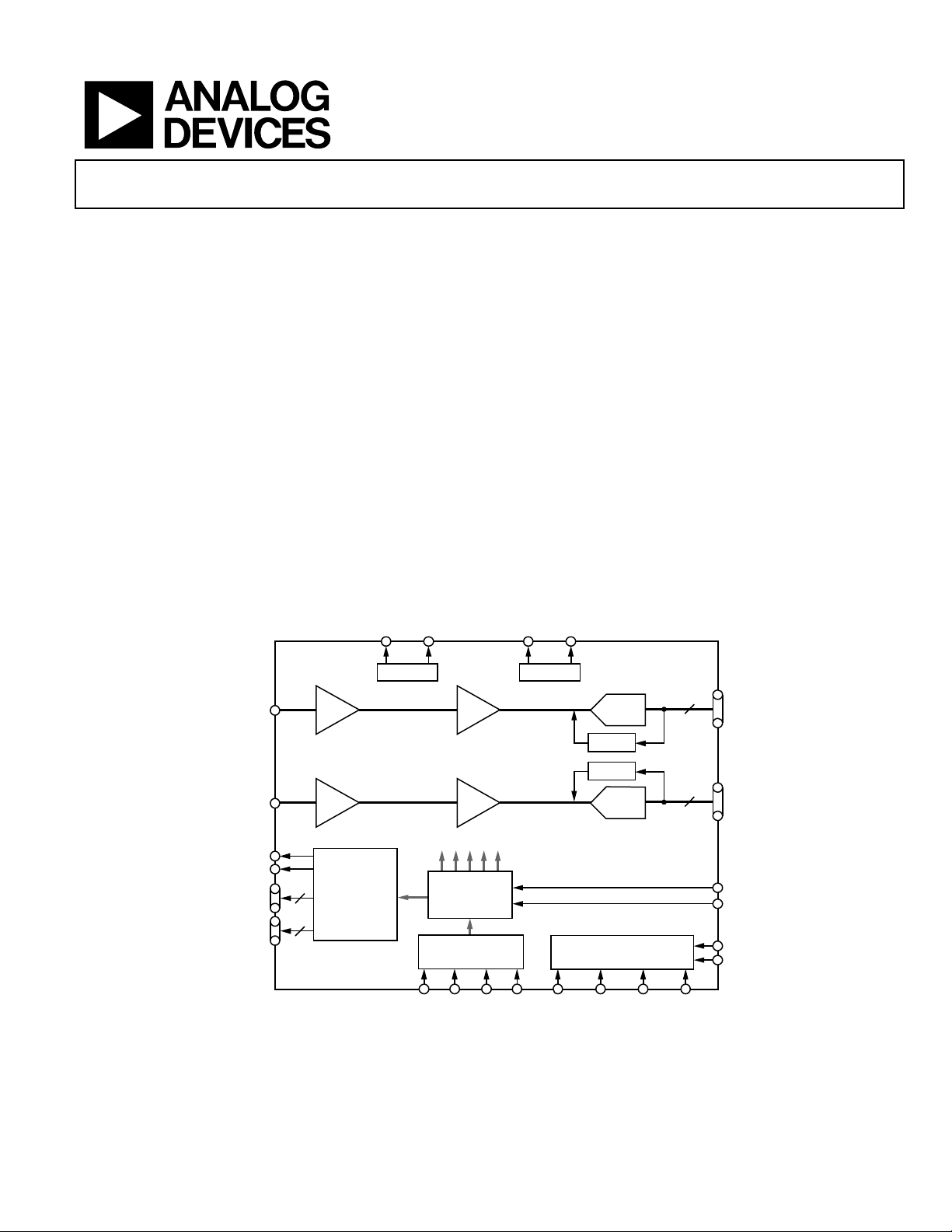
The AD9942 is a highly integrated dual-channel CCD signal
processor for digital still camera applications. Each channel is
specified at pixel rates of up to 40 MHz. The AD9942 consists of
a complete analog front end with analog-to-digital conversion,
combined with a programmable timing driver. The Precision
Timi ng Core allows high speed clocks to be adjusted with
550 ps resolution.
The analog front end uses black level clamping and includes a
VGA, a 40 MSPS ADC, and a CDS. The timing driver provides
the high speed CCD clock drivers for RG_A, RG_B, and the
H1A to H4A and H1B to H4B outputs. The 6-wire serial
interface is used to program the AD9942.
Available in a space-saving, 9 mm × 9 mm, CSP_BGA package,
the AD9942 is specified over an operating temperature range of
−25°C to +85°C.
CCDIN_A
CCDIN_B
RG_A
RG_B
H1A TO H4
H1B TO H4B
AD9942
4
4
CDS
CDS
HORIZONTAL
DRIVERS
FUNCTIONAL BLOCK DIAGRAM
0dB
0dB
Figure 1.
REFT_B REFB_B
VREF_B
~
18dB
~
18dB
SL_A
SDATA_A
REFT_A REFB_A
VREF_A
INTERNAL CLOCKS
HD_A VD_A HD_B VD_B
VGA
VGA
PRECISION
TIMING
CORE
SYNC
GENERATOR
ADC
CLAMP
CLAMP
ADC
INTERNAL
REGISTERS
SL_B
14
14
SDATA_B
DOUT_A
DOUT_B
CLI_A
CLI_B
SCK_A
SCK_B
05240-001
Rev. 0
Information furnished by Analog Devices is believed to be accurate and reliable.
However, no responsibility is assumed by Analog Devices for its use, nor for any
infringements of patents or other rights of third parties that may result from its use.
Specifications subject to change without notice. No license is granted by implication
or otherwise under any patent or patent rights of Analog Devices. Trademarks and
registered trademarks are the property of their respective owners.
One Technology Way, P.O. Box 9106, Norwood, MA 02062-9106, U.S.A.
Tel: 781.329.4700
Fax: 781.326.8703 © 2005 Analog Devices, Inc. All rights reserved.
www.analog.com
Page 2

AD9942
TABLE OF CONTENTS
General Specifications...................................................................... 3
Digital Specifications........................................................................ 4
Channel A and Channel B Horizontal Clamping
and Blanking ................................................................................... 22
Individual CLPOB and PBLK Sequences................................ 22
Analog Specifications....................................................................... 5
Channel-to-Channel Specifications ............................................... 6
Timing Specifications....................................................................... 7
Absolute Maximum Ratings............................................................ 8
Thermal Resistance ...................................................................... 8
ESD Caution.................................................................................. 8
Pin Configuration and Function Descriptions............................. 9
Te r mi n ol o g y .................................................................................... 11
Equivalent Input/Output Circuits................................................ 12
Typical Performance Characteristics ........................................... 13
System Overview ............................................................................ 14
Serial Interface Timing .................................................................. 15
Complete Register Listing......................................................... 16
Channel A and Channel B Precision Timing............................... 19
High Speed Timing Generation ............................................... 19
Timing Resolution...................................................................... 19
High Speed Clock Programmability ........................................ 19
H-Driver and RG Outputs ........................................................21
Digital Data Outputs.................................................................. 21
Individual HBLK Sequences..................................................... 22
Channel A and Channel B Special HBLK Patterns.................... 24
Horizontal Sequence Control ................................................... 24
H-Counter Synchronization..................................................... 24
Channel A and Channel B Power-Up Procedure....................... 25
Channel A and Channel B Analog Front End Operation......... 26
DC Restore .................................................................................. 26
Correlated Double Sampler ...................................................... 26
Channel A and Channel B Variable Gain Amplifier............. 27
Channel A and Channel B ADC .............................................. 27
Channel A and Channel B Optical Black Clamp ................... 27
Channel A and Channel B Digital Data Outputs................... 27
Applications Information.............................................................. 28
Circuit Configuration ................................................................ 28
Grounding/Decoupling Recommendations ........................... 28
Driving the CLI Input................................................................ 30
Horizontal Timing Sequence Example.................................... 30
Outline Dimensions ....................................................................... 32
Ordering Guide .......................................................................... 32
REVISION HISTORY
1/05—Revision 0: Initial Version
Rev. 0 | Page 2 of 32
Page 3

AD9942
GENERAL SPECIFICATIONS
In Table 1, X = A, B.
Table 1.
Parameter Min Typ Max Unit
TEMPERATURE RANGE
Operating
Storage
−25
−65
MAXIMUM CLOCK RATE 40 MHz
POWER SUPPLY VOLTAGE
AVDD_X, TCVDD_X (AFE, Timing Core) 2.7 3.0 3.6 V
HVDD_X (H1X to H4X Drivers) 2.7 3.0 3.6 V
RGVDD_X (RG_X Driver) 2.7 3.0 3.6 V
DRVDD_X (D0 to D13 Drivers) 2.7 3.0 3.6 V
DVDD_X (Digital) 2.7 3.0 3.6 V
POWER DISSIPATION FOR EACH CHANNEL
(40 MHz, 3 V Supplies, 100 pF H1X to H4X Loading, 10 pF RG_X Loading)
Power from AVDD_X 110 mW
Power from TCVDD_X 33 mW
Power from HVDD_X
1
160 mW
Power from RGVDD_X 13 mW
Power from DRVDD_X 15 mW
Power from DVDD_X 40 mW
Total Shutdown Mode 2 mW
1
Total HVDD_X Power = [(C
) × (HVDD_X) × (Pixel Frequency)] × (HVDD_X) × (Number of Horizontal Outputs Used).
LOAD
+85 °C
+150 °C
Rev. 0 | Page 3 of 32
Page 4

AD9942
DIGITAL SPECIFICATIONS
T
to T
MIN
In Table 2, X = A, B.
Table 2.
Parameter Symbol Min Typ Max Unit
LOGIC INPUTS
High Level Input Voltage V
Low Level Input Voltage V
High Level Input Current I
Low Level Input Current I
Input Capacitance CIN 10 pF
LOGIC OUTPUTS
High Level Output Voltage, IOH = 2 mA V
Low Level Output Voltage, IOL = 2 mA VOL 0.5 V
CLI INPUT
High Level Input Voltage (TCVDD_X/2 + 0.5 V) V
Low Level Input Voltage V
RG_X AND H1X TO H4X DRIVER OUTPUTS
High Level Output Voltage (RGVDD_X – 0.5 V and HVDD_X – 0.5 V) VOH 2.2 V
Low Level Output Voltage V
Maximum Output Current (Programmable) 30 mA
Maximum Load Capacitance 100 pF
, AVDD_X = DVDD_X = DRVDD_X = HVDD_X = RGVDD_X = 2.7 V, CL = 20 pF, unless otherwise noted.
MAX
IH
IL
IH
IL
OH
IH – CLI
IL – CLI
OL
2.1 V
0.6 V
10 µA
10 µA
2.2 V
1.85 V
0.85 V
0.5 V
Rev. 0 | Page 4 of 32
Page 5
AD9942
ANALOG SPECIFICATIONS
T
to T
MIN
Table 3.
Parameter Min Typ Max Unit Notes
CDS
Gain 0 dB
Allowable CCD Reset Transient
Max Input Range before Saturation 1.0 V p-p
Max CCD Black Pixel Amplitude ±100 mV Measured at 12 dB VGA gain
VARIABLE GAIN AMPLIFIER (VGA_X)
Max Input Range 1.0 V p-p
Max Output Range 2.0 V p-p
Gain Control Resolution 512 Steps
Gain Monotonicity Guaranteed
Gain Range
BLACK LEVEL CLAMP
Clamp Level Resolution 256 Steps 4 LSB/step
Clamp Level Measured at ADC output
CHN_A AND CHN_B ADC
Differential Nonlinearity (DNL) −1.0 ± 0.5 +1.0 LSB
No Missing Codes Guaranteed
Full-Scale Input Voltage 2.0 V
VOLTAGE REFERENCE
Reference Top Voltage (REFT_X) 2.0 V
Reference Bottom Voltage (REFB_X) 1.0 V
SYSTEM PERFORMANCE Specifications include entire signal chain
VGA Gain Accuracy
Peak Nonlinearity, 500 mV Input Signal 0.15 % 12 dB gain applied
Total Output Noise 3 LSB rms AC grounded input, 6 dB gain applied
Power Supply Rejection (PSR) 50 dB Measured with step change on supply
1
Input signal characteristics defined as follows:
, AVDD_X = DVDD_X = 3.0 V, f
MAX
1
= 40 MHz, typical timing specifications, unless otherwise noted. In Table 3, X = A, B.
CLI
500 mV
Min Gain (Code 0) 0 dB
Max Gain (Code 511) 18 dB
Min Clamp Level 0 LSB
Max Clamp Level 1023 LSB
Min Gain (Code 0) 5 5.5 6 dB
Max Gain (Code 511) 17.5 18 18.5 dB
(Typ = 70 mV at 15 dB and 50 mV at 18 dB)
500mV TYP
RESET TRANSIENT
OPTICAL BLACK PIXEL
100mV MAX
1V MAX
INPUT SIGNAL RANGE
05240-099
Rev. 0 | Page 5 of 32
Page 6
AD9942
CHANNEL-TO-CHANNEL SPECIFICATIONS
T
to T
MIN
Table 4.
Parameter Min Typ Max Unit Notes
CHANNEL A/CHANNEL B OUTPUT
CODE MATCHING ERROR
CROSSTALK ERROR VGA = 6 dB, 12 dB, and 18 dB conditions.
Channel A to Channel B
Channel B to ChannelA
1
Matching error calculated using a ramp input applied to Channel A and Channel B simultaneously. Typical Channel A/Channel B error is < 1.0% at each output code.
, AVDD_X = DVDD_X = 3.0 V, f
MAX
1
= 40 MHz, typical timing specifications, unless otherwise noted. In Table 4, X = A, B.
CLI
< 1.0 % VGA = 6 dB, 12 dB, and 18 dB conditions.
−84
dB
Full-scale step applied to Channel A while
measuring response on Channel B.
−84
dB
Full-scale step applied to Channel B while
measuring response on Channel A.
Rev. 0 | Page 6 of 32
Page 7
AD9942
TIMING SPECIFICATIONS
CL = 20 pF, f
Table 5.
Parameter Symbol Min Typ Max Unit
MASTER CLOCK (CLI_X) (See Figure 16)
CLI_X Clock Period 25.0 ns
CLI_X High/Low Pulse Width t
Delay from CLI_X to Internal Pixel
Period Position (See Figure 16) t
CLPOB_X PULSE WIDTH (Programmable)
SAMPLE CLOCKS (See Figure 18)
SHP_X Rising Edge to SHD_X Rising Edge t
DATA OUTPUTS (See Figure 19 and Figure 20)
Output Delay from Programmed Edge t
Pipeline Delay 11 Cycles
SERIAL INTERFACE
Maximum SCK_X Frequency f
SL_X to SCK_X Setup Time t
SCK to SL_X Hold Time t
SDATA_X Valid to SCK_X Rising Edge Setup t
SCK_X Falling Edge to SDATA_X Valid Hold t
SCK_X Falling Edge to SDATA_X Valid Read t
1
Minimum CLPOB pulse width is for functional operation only. Wider typical pulses are recommended to achieve low noise clamp reference.
= 40 MHz, serial timing in Figure 14 and Figure 15, unless otherwise noted. In Table 5, X = A, B.
CLI
ADC
1
CLIDLY
t
2 20 Pixels
COB
S1
OD
SCLK
LS
LH
DS
DH
DV
10.0 12.5 15.0 ns
6 ns
11.2 12.5 ns
6 ns
10 MHz
10 ns
10 ns
10 ns
10 ns
10 ns
Rev. 0 | Page 7 of 32
Page 8
AD9942
ABSOLUTE MAXIMUM RATINGS
Table 6. Ratings (X = A, B)
Parameter Rating
AVDD_X and TCVDD_X to AVSS_X −0.3 V to +3.9 V
HVDD_X and RGVDD_X to
HVSS_X and RGVSS_X
DVDD_X and DRVDD_X to
DVSS_X and DRVSS_X
Any VSS_X to Any VSS_X −0.3 V to +0.3 V
Digital Outputs to DRVSS_X −0.3 V to DRVDD + 0.3 V
SCK_X, SL_X, and SDATA_X to
DVSS_X
RG_X to RGVSS_X −0.3 V to RGVDD + 0.3 V
H1X to H4X to HVSS_X −0.3 V to HVDD + 0.3 V
REFT_X, REFB_X, and CCDIN_X to
AVSS_X
Junction Temperature 150°C
Lead Temperature (10 sec) 300°C
−0.3 V to +3.9 V
−0.3 V to +3.9 V
−0.3 V to DVDD + 0.3 V
−0.3 V to AVDD + 0.3 V
Stresses above those listed under Absolute Maximum Ratings
may cause permanent damage to the device. This is a stress
rating only; functional operation of the device at these or any
other conditions above those listed in the operational sections
of this specification is not implied. Exposure to absolute
maximum rating conditions for extended periods may affect
device reliability.
THERMAL RESISTANCE
100-lead, 9 mm × 9 mm, CSP_BGA package: θJA = 38.3°C/W
1
θJA is measured using a 4-layer PCB with the exposed paddle soldered to the
board.
1
ESD CAUTION
ESD (electrostatic discharge) sensitive device. Electrostatic charges as high as 4000 V readily accumulate on
the human body and test equipment and can discharge without detection. Although this product features
proprietary ESD protection circuitry, permanent damage may occur on devices subjected to high energy
electrostatic discharges. Therefore, proper ESD precautions are recommended to avoid performance
degradation or loss of functionality.
Rev. 0 | Page 8 of 32
Page 9
AD9942
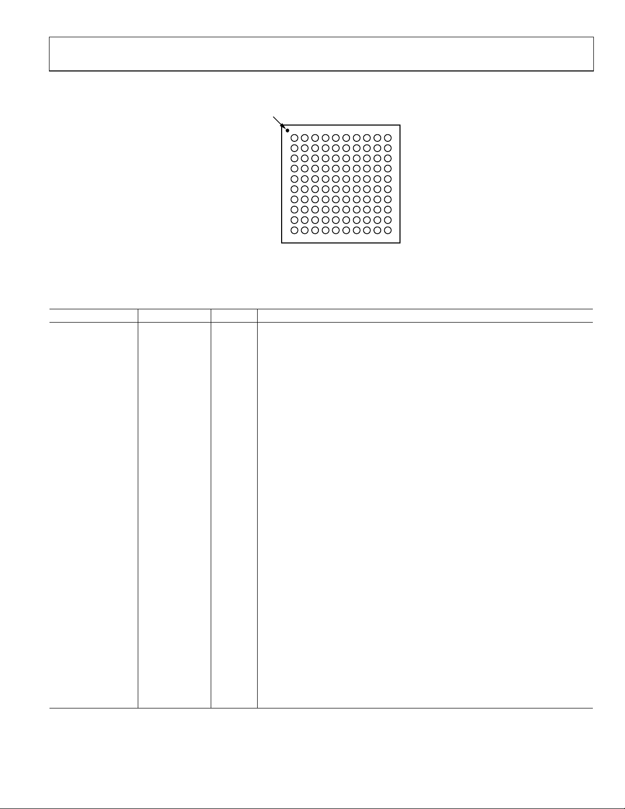
PIN CONFIGURATION AND FUNCTION DESCRIPTIONS
A1 CORNER
INDEX AREA
Table 7. Pin Function Descriptions
Ball Location Mnemonic Type1 Description
B2 SL_A DI 6-Wire Serial Load for Channel A
C2 SDATA_A DI 6-Wire Serial Data for Channel A
D2 SCK_A DI 6-Wire Serial Clock for Channel A
C1 REFT_A AO Reference Top Decoupling for Channel A (decouple with 1.0 µF to AVSS_A)
D1 REFB_A AO Reference Bottom Decoupling for Channel A (decouple with 1.0 µF to AVSS_A)
A1 CCDIN_A AI Analog Input for Channel A CCD Signal (connect through Series 0.1 µF capacitor)
F4 H1A DO CCD Horizontal Clock 1 for Channel A
F3 H2A DO CCD Horizontal Clock 2 for Channel A
D4 H3A DO CCD Horizontal Clock 3 for Channel A
D3 H4A DO CCD Horizontal Clock 4 for Channel A
B4 RG_A DO CCD Reset Gate Clock for Channel A
J2 DRVSS_A P Digital Driver Ground for Channel A
K3 DRVDD_A P Digital Driver Supply for Channel A
E3 HVSS_A P H1A to H4A Driver Ground for Channel A
E4 HVDD_A P H1A to H4A Driver Supply for Channel A
C3 RGVSS_A P RG_A Driver Ground for Channel A
C4 RGVDD_A P RG_A Driver Supply for Channel A
B3 TCVSS_A P Analog Ground for Channel A Timing Core
A4 TCVDD_A P Analog Supply for Channel A Timing Core
B1 AVSS_A P Analog Ground for Channel A
A2 AVDD_A P Analog Ground for Channel A
F2 DVSS_A P Digital Ground for Channel A
F1 DVDD_A P Digital Supply for Channel A
E2 VD_A DI Vertical Sync Pulse for Channel A
E1 HD_A DI Horizontal Sync Pulse for Channel A
B8 SL_B DI 6-Wire Serial Load for Channel B
C8 SDATA_B DI 6-Wire Serial Data for Channel B
D8 SCK_B DI 6-Wire Serial Clock for Channel B
C7 REFT_B AO Reference Top Decoupling for Channel B (decouple with 1.0 µF to AVSS_B)
D7 REFB_B AO Reference Bottom Decoupling for Channel B (decouple with 1.0 µF to AVSS_B)
A7 CCDIN_B AI Analog Input for Channel B CCD Signal (connect through series 0.1 µF capacitor)
1
Type: AI = Analog Input, AO = Analog Output, DI = Digital Input, DO = Digital Output, P = Power.
1
2345678910
A
B
C
D
E
F
G
H
J
K
AD9942
TOP VIEW
(Not to Scale)
Figure 2. Pin Configuration
05240-002
Rev. 0 | Page 9 of 32
Page 10
AD9942
Ball Location Mnemonic Type1 Description
F10 H1B DO CCD Horizontal Clock 1 for Channel B
F9 H2B DO CCD Horizontal Clock 2 for Channel B
D10 H3B DO CCD Horizontal Clock 3 for Channel B
D9 H4B DO CCD Horizontal Clock 4 for Channel B
B10 RG_B DO CCD Reset Gate Clock for Channel B
J8 DRVSS_B P Digital Driver Ground for Channel B
K9 DRVDD_B P Digital Driver Supply for Channel B
E9 HVSS_B P H1B to H4B Driver Ground for Channel B
E10 HVDD_B P H1B to H4B Driver Supply for Channel B
C9 RGVSS_B P RG_B Driver Ground for Channel B
C10 RGVDD_B P RG_B Driver Supply for Channel B
B9 TCVSS_B P Analog Ground for Channel B Timing Core
A10 TCVDD_B P Analog Supply for Channel B Timing Core
B7 AVSS_B P Analog Ground for Channel B
A8 AVDD_B P Analog Ground for Channel B
F8 DVSS_B P Digital Ground for Channel B
F7 DVDD_B P Digital Supply for Channel B
E8 VD_B DI Vertical Sync Pulse for Channel B
E7 HD_B DI Horizontal Sync Pulse for Channel B
A3 CLI_A DI Master Clock Input for Channel A
G1 D0_A DO Data Outputs Channel A
H1 D1_A DO Data Outputs Channel A
J1 D2_A DO Data Outputs Channel A
K1 D3_A DO Data Outputs Channel A
G2 D4_A DO Data Outputs Channel A
H2 D5_A DO Data Outputs Channel A
K2 D6_A DO Data Outputs Channel A
G3 D7_A DO Data Outputs Channel A
H3 D8_A DO Data Outputs Channel A
J3 D9_A DO Data Outputs Channel A
K4 D10_A DO Data Outputs Channel A
J4 D11_A DO Data Outputs Channel A
H4 D12_A DO Data Outputs Channel A
G4 D13_A DO Data Outputs Channel A
A5, B5, C5, D5, E5,
F5, G5, H5, J5, K5
A9 CLI_B DI Master Clock Input for Channel B
G7 D0_B DO Data Outputs Channel B
H7 D1_B DO Data Outputs Channel B
J7 D2_B DO Data Outputs Channel B
K7 D3_B DO Data Outputs Channel B
G8 D4_B DO Data Outputs Channel B
H8 D5_B DO Data Outputs Channel B
K8 D6_B DO Data Outputs Channel B
G9 D7_B DO Data Outputs Channel B
H9 D8_B DO Data Outputs Channel B
J9 D9_B DO Data Outputs Channel B
K10 D10_B DO Data Outputs Channel B
J10 D11_B DO Data Outputs Channel B
H10 D12_B DO Data Outputs Channel B
G10 D13_B DO Data Outputs Channel B
A6, B6, C6, D6, E6,
F6, G6, H6, J6, K6
GND P Ground Connection
GND P Ground Connection
Rev. 0 | Page 10 of 32
Page 11

AD9942
TERMINOLOGY
Differential Nonlinearity (DNL)
An ideal ADC exhibits code transitions that are exactly 1 LSB
apart. DNL is the deviation from this ideal value. Therefore,
every code must have a finite width. No missing codes
guaranteed to 12-bit resolution indicates that all 4096 codes,
respectively, must be present over all operating conditions.
Peak Nonlinearity
Peak nonlinearity, a full signal chain specification, refers to the
peak deviation of the output of the AD9942 from a true straight
line. The point used as zero scale occurs 0.5 LSB before the first
code transition. Positive full scale is defined as a level 1 LSB
and 0.5 LSB beyond the last code transition. The deviation is
measured from the middle of each particular output code to the
true straight line. The error is then expressed as a percentage
of the 2 V ADC full-scale signal. The input signal is always
appropriately gained up to fill the ADC’s full-scale range.
Tot a l O ut p ut Noi s e
The rms output noise is measured using histogram techniques.
The standard deviation of the ADC output codes is calculated
in LSBs and represents the rms noise level of the total signal
chain at the specified gain setting. The output noise can be
converted to an equivalent voltage, using the relationship
n
1 LSB = (ADC full scale/2
codes)
Power Supply Rejection (PSR)
The PSR is measured with a step change applied to the supply
pins. The PSR specification is calculated from the change in the
data outputs for a given step change in the supply voltage.
Matching Error
The matching error refers to the Channel A to Channel B
mismatch after post ADC correction calibration has been
applied to remove gain error between Channel A and
Channel B.
Crosstalk
The crosstalk is measured while applying a full-scale step to
one channel while measuring the interference on the opposite
channel.
)(
LSBceInterferen
Crosstalk
⎛
×=
LOG20)dB(
⎜
16384
⎝
⎞
⎟
⎠
where n is the bit resolution of the ADC. For the AD9942,
1 LSB is approximately 122.0 µV.
Rev. 0 | Page 11 of 32
Page 12

AD9942
C
EQUIVALENT INPUT/OUTPUT CIRCUITS
In Figure 3 through Figure 7, X = A, B.
AVDD
DVDD
DATA
R
AVSS
AVSS
05240-003
Figure 3. CCDIN_X
AVDD
330Ω
AVSS
25kΩ
1.4V
+
05240-004
LI
DATA
ENABLE DOUT
Figure 4. CLI_X
330Ω
DVSS
Figure 6. Digital Inputs
HVDD OR RGVDD
HVSS OR RGVSS
Figure 7. H1X to H4X and RG_X
05240-006
05240-007
DVSS
DRVDD
THREE-STATE DOUT
DVSS DRVSS
05240-005
Figure 5. Data Outputs D0_X to D13_X
Rev. 0 | Page 12 of 32
Page 13

AD9942
TYPICAL PERFORMANCE CHARACTERISTICS
1.0
1.015
0.5
0
LSB
–0.5
–1.0
0 4000 8000 12000 16000
ADC OUTPUT CODE
Figure 8. Typical DNL for Channel A and Channel B
10
5
0
–5
LSB
–10
–15
–20
DAC OUTPUT CODE
160001400012000100008000600040002000
Figure 9. Typical INL Performance for Channel A and Channel B
05240-008
05240-009
1.010
1.005
1.000
CHANNEL A/CHANNEL B RATIO
0.995
ADC OUTPUT CODE
–25°C +25°C
+85°C
Figure 10. Typical Noncalibrated Channel A/Channel B Ratio
05240-010
160001400012000100008000600040002000
Rev. 0 | Page 13 of 32
Page 14

AD9942
SYSTEM OVERVIEW
V-DRIVER
H1A TO H4A, RG_A
H1B TO H4B, RG_B
CCDIN_A
CCD
CCDIN_B
AD9942
INTEGRATED
AFE + TD
SERIAL
INTERFACE
Figure 11. Typical Application
V1 > Vx, VSG1 > VSGx, SUBCK
DOUT
DIGITAL IMAGE
HD_A, VD_A,
HD_B, VD_B
CLI_A, CLI_B
PROCESSING
ASIC
05240-014
MAXIMUM FIELD DIMENSIONS
12-BIT HORIZONTAL = 4096 PIXELS MAX
12-BIT VERTICAL = 4096 LINES MAX
05240-015
Figure 12. Vertical and Horizontal Counters
Figure 11 shows the typical system application diagram for the
AD9942. The CCD output is processed by the AD9942 AFE
circuitry, which consists of a CDS, VGA, a black level clamp,
and an ADC. The digitized pixel information is sent to the
digital image processor chip, where all postprocessing and
compression occurs. To operate the CCD, CCD timing parameters are programmed from the image processor to the AD9942
through the 6-wire serial interface. From the system master
clock, CLI, provided by the image processor, the device
generates the high speed CCD clocks and all internal AFE
clocks. All AD9942 clocks are synchronized with VD_X and
HD_X. The CLPOB is programmed and generated internally.
MAX VD LENGTH IS 4095 LINES
VD_X
HD_X
CLI_X
MAX HD LENGTH IS 4095 PIXELS
Figure 13. Maximum VD_X/HD_X Dimensions
The H-drivers for H1A to H4A, H1B to H4B, RG_A and RG_B
are included in the AD9942, allowing these clocks to be directly
connected to the CCD. H-drive voltage of 3 V is supported in
the AD9942.
Figure 12 shows the horizontal and vertical counter dimensions
for the device. All internal horizontal clocking is programmed
using these dimensions to specify line and pixel locations.
05240-016
Rev. 0 | Page 14 of 32
Page 15

AD9942
SERIAL INTERFACE TIMING
All of the AD9942 internal registers are accessed through a
6-wire serial interface. Each register consists of an 8-bit address
and a 24-bit data-word. Both the 8-bit address and 24-bit dataword are written starting with the LSB. To write to each register,
a 32-bit operation is required, as shown in Figure 14. Although
many registers are less than 24 bits wide, all 24 bits must be
written for each register. If the register is only 16 bits wide, then
the upper 8 bits may be filled with 0s during the serial write
operation. If fewer than 24 bits are written, the register is not
updated with new data.
8-BIT ADDRESS
Figure 15 shows a more efficient way to write to the registers by
using the AD9942 address auto-increment capability. In this
method, the lowest desired address is written first, followed by
multiple 24-bit data-words. Each new 24-bit data-word is
written automatically to the next highest register address. By
eliminating the need to write each 8-bit address, faster register
loading is achieved. Address auto-increment can be used,
starting with any register location, to write to as few as two
registers or to as many as the entire register space.
24-BIT DATA
SDATA_X
SCK_X
SDATA_X
...
...
...
...
t
LH
SL UPDATED VD/HD UPDATED
SL_X
VD_X
A0 A1 A2 A4 A5 A6 A7
1 322 3 4 5 6 7 8 9 10 11 12 30 31
t
LS
A3
t
DS
t
DH
D1 D2 D3 D21 D22 D23
D0
...
HD_X
NOTES
1. X = A, B
2. INDIVIDUAL SDATA_X BITS ARE LATCHED ON SCK_X RISING EDGES.
3. ALL 32 BITS MUST BE WRITTEN: 8 BITS FOR ADDRESS AND 24 BITS FOR DATA.
4. IF THE REGISTER LENGTH IS <24 BITS, THEN DON’T CARE BITS MUST BE USED TO COMPLETE THE 24-BIT DATA LENGTH.
5. NEW DATA IS UPDATED AT EITHER THE SL_X RISING EDGE OR AT THE HD_X FALLING EDGE AFTER THE NEXT VD_X FALLING EDGE.
6. VD_X/HD_X UPDATE POSITION MAY BE DELAYED TO ANY HD_X FALLING EDGE IN THE FIELD USING THE UPDATE REGISTER.
Figure 14. Serial Write Operation
DATA FOR STARTING
REGISTER ADDRESS
A0 A1 A2 A4 A5 A6 A7 D0 D1 D22 D23
A3
...
DATA FOR NEXT
REGISTER ADDRESS
D0 D1 D22 D23
...
D0
05240-017
...
D2D1
SCK_X
SL_X
1 322345678910 31
NOTES
1. X = A, B
2. MULTIPLE SEQUENTIAL REGISTERS MAY BE LOADED CONTINUOUSLY.
3. THE FIRST (LOWEST ADDRESS) REGISTER ADDRESS IS WRITTEN, FOLLOWED BY MULTIPLE 24-BIT DATA-WORDS.
4. THE ADDRESS WILL AUTOMATICALLY INCREMENT WITH EACH 24-BIT DATA-WORD (ALL 24 BITS MUST BE WRITTEN).
5. SL_X IS HELD LOW UNTIL THE LAST DESIRED REGISTER HAS BEEN LOADED.
6. NEW DATA IS UPDATED AT EITHER THE SL RISING EDGE OR AT THE HD FALLING EDGE AFTER THE NEXT VD FALLING EDGE.
...
...
...
3433 5655
...
Figure 15. Continuous Serial Write Operation
Rev. 0 | Page 15 of 32
585759
...
...
05240-018
Page 16

AD9942
COMPLETE REGISTER LISTING
In Table 8 through Table 16, note the following:
• All addresses and default values are expressed in hexadecimal.
• All registers are VD_X/HD_X updated as shown in Figure 14, except for the registers indicated in Table 8, which are SL_X updated.
• Each channel is programmed independently using the 5-wire serial interface. Both channels can be programmed with the same register
values by tying the SL_A and SL_B signals together and the SDATA_A and SDATA_B signals together.
Table 8. Updated Registers on Rising Edge of SL_X
Register Description
OPRMODE AFE operation modes
CTLMODE AFE control modes
SW_RESET Software reset bit
TGCORE _RSTB Reset bar signal for internal TG core
PREVENTUPDATE Prevents update of registers
VDHDEDGE VD/HD active edge
FIELDVAL Resets internal field pulse
HBLKRETIME Retimes the HBLK to internal clock
H1CONTROL H1 polarity control
RGCONTROL RG signal control polarity
DRVCONTROL Drive-strength control
SAMPCONTROL SHP/SHD sample control
DOUTPHASE DOUT phase control
Table 9. CHN_A and CHN_B AFE Register Map
Address Data Bit Content Default Name Description
00 [11:0] 4 OPRMODE AFE operation modes. (See Table 15.)
01 [9:0] 0 TEST MODE Internal test mode. Should always be set = 0.
02 [7:0] 80 CLAMP LEVEL Optical black clamp level.
03 [11:0] 4 CTLMODE AFE control modes. (See Table 16.)
04 [17:0] 0 TESTMODE Test operation only. Set = 0.
05 [17:0] 0 TESTMODE Test operation only. Set = 0.
Table 10. CHN_A and CHN_B Miscellaneous Register Map
Address Data Bit Content Default Name Description
10 [0] 0 SW_RST Software reset.1 = reset all registers to default, then self-clear back to 0.
11 [0] 0 OUT_CONTROL Output control. 0 = make all dc outputs inactive.
12 [0] 0 TGCORE_RSTB Timing core reset bar. 0 = reset TG core; 1 = resume operation.
13 [11:0] 0 UPDATE Serial update. Sets the line (HD) within the field to update serial data.
14 [0] 0 PREVENTUPDATE Prevents the update of the VD updated registers. 1 = prevent update.
15 [0] 0 VDHDEDGE
16 [1:0] 0 FIELDVAL
17 [0] 0 HBLKRETIME
18 [1:0] 0 TEST MODE Internal test mode. Should always be set = 0.
19 [0] 0 TEST MODE Internal test mode. Should always be set = 0.
1A [0] 0 TEST MODE Internal test mode. Should always be set = 0.
E8 [2:0]
[11:3]
0
0
TEST MODE
VGAGAIN
VD/HD active edge.
0 = falling edge triggered; 1 = rising edge triggered.
Field value sync.
0 = next field 0; 1 = next field 1; 2/3 = next field 2.
Retime HBLK to internal H1 clock. Preferred setting is 1. Setting to 1
adds one cycle delay to HBLK toggle positions.
Internal test mode. Should always be set = 0.
VGA gain control.
Rev. 0 | Page 16 of 32
Page 17

AD9942
Table 11. CHN_A and CHN_B CLPOB Register Map
Address Data Bit Content Default (Hex) Name Description (the CLPOBSCP0 Always Starts at Line 0)
20 [3:0] F CLPOBPOL Start polarities for CLPOB Sequences 0, 1, 2, and 3.
21 [23:0] FFFFFF CLPOBTOG_0 Sequence 0. Toggle Position 1 [11:0] and Toggle Position 2 [23:12].
22 [23:0] FFFFFF CLPOBTOG_1 Sequence 1. Toggle Position 1 [11:0] and Toggle Position 2 [23:12].
23 [23:0] FFFFFF CLPOBTOG_2 Sequence 2. Toggle Position 1 [11:0] and Toggle Position 2 [23:12].
24 [23:0] FFFFFF CLPOBTOG_3 Sequence 3. Toggle Position 1 [11:0] and Toggle Position 2 [23:12].
25 [7:0] 00 CLPOBSPTR CLPOB sequence pointers for Region 0 [1:0], 1 [3:2], 2 [5:4], 3 [7:6].
26 [11:0] FFF CLPOBSCP1 CLPOB Sequence—Change Position 1.
27 [11:0] FFF CLPOBSCP2 CLPOB Sequence—Change Position 2.
28 [11:0] FFF CLPOBSCP3 CLPOB Sequence—Change Position 3.
Table 12. PBLK Register Map
Address Data Bit Content Default (Hex) Name Description (the PBLKSCP0 Always Starts at Line 0)
30 [3:0] F PBLKPOL Start polarities for PBLK Sequences 0, 1, 2, and 3.
31 [23:0] FFFFFF PBLKTOG_0 Sequence 0. Toggle Position 1 [11:0] and Toggle Position 2 [23:12].
32 [23:0] FFFFFF PBLKTOG_1 Sequence 1. Toggle Position 1 [11:0] and Toggle Position 2 [23:12].
33 [23:0] FFFFFF PBLKTOG_2 Sequence 2. Toggle Position 1 [11:0] and Toggle Position 2 [23:12].
34 [23:0] FFFFFF PBLKTOG_3 Sequence 3. Toggle Position 1 [11:0] and Toggle Position 2 [23:12].
35 [7:0] 00 PBLKSPTR PBLK Sequence Pointers for Region 0 [1:0], 1 [3:2], 2 [5:4], 3 [7:6].
36 [11:0] FFF PBLKSCP1 PBLK Sequence—Change Position 1.
37 [11:0] FFF PBLKSCP2 PBLK Sequence—Change Position 2.
38 [11:0] FFF PBLKSCP3 PBLK Sequence—Change Position 3.
Table 13. HBLK Register Map
Address Data Bit Content Default (Hex) Name Description (the HBLKSCP0 Always Starts at Line 0)
40 [0] 0 HBLKDIR HBLK internal/external. 0 = internal; 1 = external.
41 [0] 0 HBLKPOL HBLK external active polarity. 0 = active low; 1 = active high.
42 [0] 1 HBLKEXTMASK HBLK external masking polarity. 0 = mask H1 low; 1 = mask H1 high.
43 [3:0] F HBLKMASK HBLK internal masking polarity. 0 = mask H1 low; 1 = mask H1 high.
44 [23:0] FFFFFF HBLKTOG12_0 Sequence 0. Toggle Position 1 [11:0] and Toggle Position 2 [23:12].
45 [23:0] FFFFFF HBLKTOG34_0 Sequence 0. Toggle Position 3 [11:0] and Toggle Position 4 [23:12].
46 [23:0] FFFFFF HBLKTOG56_0 Sequence 0. Toggle Position 5 [11:0] and Toggle Position 6 [23:12].
47 [23:0] FFFFFF HBLKTOG12_1 Sequence 1. Toggle Position 1 [11:0] and Toggle Position 2 [23:12].
48 [23:0] FFFFFF HBLKTOG34_1 Sequence 1. Toggle Position 3 [11:0] and Toggle Position 4 [23:12].
49 [23:0] FFFFFF HBLKTOG56_1 Sequence 1. Toggle Position 5 [11:0] and Toggle Position 6 [23:12].
4A [23:0] FFFFFF HBLKTOG12_2 Sequence 2. Toggle Position 1 [11:0] and Toggle Position 2 [23:12].
4B [23:0] FFFFFF HBLKTOG34_2 Sequence 2. Toggle Position 3 [11:0] and Toggle Position 4 [23:12].
4C [23:0] FFFFFF HBLKTOG56_2 Sequence 2. Toggle Position 5 [11:0] and Toggle Position 6 [23:12].
4D [23:0] FFFFFF HBLKTOG12_3 Sequence 3. Toggle Position 1 [11:0] and Toggle Position 2 [23:12].
4E [23:0] FFFFFF HBLKTOG34_3 Sequence 3. Toggle Position 3 [11:0] and Toggle Position 4 [23:12].
4F [23:0] FFFFFF HBLKTOG56_3 Sequence 3. Toggle Position 5 [11:0] and Toggle Position 6 [23:12].
50 [7:0] 00 HBLKSPTR HBLK sequence pointers for Region 0 [1:0], 1 [3:2], 2 [5:4], 3 [7:6].
51 [11:0] FFF HBLKSCP1 HBLK Sequence—Change Position 1.
52 [11:0] FFF HBLKSCP2 HBLK Sequence—Change Position 2.
53 [11:0] FFF HBLKSCP3 HBLK Sequence—Change Position 3.
Rev. 0 | Page 17 of 32
Page 18

AD9942
Table 14. CHN_A and CHN_B H1 to H4, RG, SHP, SHD Register Map
Address Data Bit Content Default Name Description
60 [12:0] 01001 H1CONTROL
61 [12:0] 00801 RGCONTROL
62 [14:0] 0 DRVCONTROL
63 [11:0] 00024 SAMPCONTROL
64 [5:0] 0 DOUTPHASE DOUT phase control.
Table 15. CHN_A and CHN_B AFE Operation Register Detail
Address Data Bit Content Default Name Description
00 [1:0] 0 PWRDOWN 0 = normal operation; 1 = reference standby; 2/3 = total power-down.
[2] 1 CLPENABLE 0 = disable OB clamp; 1 = enable OB clamp.
[3] 0 CLPSPEED 0 = select normal OB clamp settling; 1 = select fast OB clamp settling.
[4] 0 FASTUPDATE 0 = ignore VGA update; 1 = very fast clamping when VGA is updated.
[5] 0 PBLK_LVL DOUT value during PBLK; 0 = blank to zero; 1 = blank to clamp level.
[7:6] 0 TEST MODE Internal test mode. Should always be set = 3.
[8] 0 DCBYP 0 = enable DC restore circuit; 1 = bypass dc restore circuit during PBLK.
[9] 0 TESTMODE Test operation only. Set = 0.
[11:10] 0 TESTMODE Test operation only. Set = 0.
Table 16. CHN_A and CHN_B AFE Control Register Detail
Address Data Bit Content Default Name Description
03 [1:0] 0 TESTMODE Test operation only. Set = 0.
[2] 1 TESTMODE Test operation only. Set = 0.
[3] 0 DOUTDISABLE 0 = data outputs are driven; 1 = data outputs are three-stated.
[4] 0 DOUTLATCH 0 = latch data outputs with DOUT phase; 1 = output latch transparent.
[5] 0 GRAYENCODE 0 = binary encode data outputs; 1= gray encode data outputs.
H1 signal control. Polarity [0] (0 = inversion; 1 = no inversion).
H1 positive edge location [6:1].
H1 negative edge location [12:7].
RG signal control. Polarity [0] (0 = inversion; 1 = no inversion).
RG positive-edge location [6:1].
RG negative-edge location [12:7].
Drive-strength control for H1X [2:0], H2X [5:3], H3X [8:6], H4X [11:9], and
RG_X [14:12].
Drive-current values: 0 = off, 1 = 4.3 mA, 2 = 8.6 mA, 3 = 12.9 mA,
4 = 17.2 mA, 5 = 21.5 mA, 6 = 25.8 mA, 7 = 30.1 mA.
SHP/SHD sample control. SHP sampling location [5:0]. SHD sampling
location [11:6].
Rev. 0 | Page 18 of 32
Page 19

AD9942
CHANNEL A AND CHANNEL B PRECISION TIMING
HIGH SPEED TIMING GENERATION
The AD9942 generates flexible high speed timing signals using
the Precision Timing Core for both channels. This core is the
foundation for generating the timing used for both the CCD
and the AFE, the reset gate RG_X, the horizontal drivers H1X
to H4X, and the SHP/SHD sample clocks. A unique architecture
makes it routine for the system designer to optimize image
quality by providing precise control over the horizontal CCD
readout and the AFE correlated double sampling.
TIMING RESOLUTION
The Precision Timing Core uses a 1× master clock input (CLI) as
a reference. This clock should be the same as the CCD pixel
clock frequency. Figure 16 illustrates how the internal timing
core divides the master clock period into 48 steps or edge
positions. Therefore, the edge resolution of the Precision Timing
Core is (t
refer to the Applications Information section.
/48). For more information on using the CLI input,
CLI
POSITION
CLI_X
1 PIXEL
PERIOD
t
CLIDLY
P[0] P[48] = P[0]P[12] P[24] P[36]
...
HIGH SPEED CLOCK PROGRAMMABILITY
Figure 17 shows how the high speed clocks, RG_X, H1X to
H4X, SHP, and SHD, are generated. The RG_X pulse has
programmable rising and falling edges and may be inverted
using the polarity control. The horizontal clock, H1, has
programmable rising and falling edges, and polarity control.
The H2 clock is always the inverse of H1. Table 17 summarizes
the high speed timing registers and their parameters.
Each edge location setting is 6 bits wide, but only 48 valid edge
locations are available. Therefore, the register values are
mapped into 4 quadrants, with each quadrant containing
12 edge locations. Table 18 shows the correct register values for
the corresponding edge locations.
...
NOTES
1. PIXEL CLOCK PERIOD IS DIVIDED INTO 48 POSITIONS, PROVIDING FINE EDGE RESOLUTION FOR HIGH SPEED CLOCKS.
2. THERE IS A FIXED DELAY FROM THE CLI_X INPUT TO THE INTERNAL PIXEL PERIOD POSITIONS (
Figure 16. High Speed Clock Resolution from CLI Master Clock Input
3
CCD SIGNAL
RG_X
H1X/H3X
H2X/H4X
12
56
PROGRAMMABLE CLOCK POSITIONS:
1. RG_X RISING EDGE.
2. RG_X FALLING EDGE.
3. SHP SAMPLE LOCATION.
4. SHD SAMPLE LOCATION.
5. H1X/H3X RISING EDGE POSITION.
6. H1X/H3X RISING EDGE POSITION (H2X/H4X ARE INVERSE OF H1X/H3X).
Figure 17. High Speed Clock Programmable Locations
4
t
CLIDLY
= 6ns TYP).
05240-019
05240-020
Rev. 0 | Page 19 of 32
Page 20

AD9942
Table 17. Channel A and Channel B H1X to H4X CONTROL, RG_X CONTROL, DRVCONTROL, and SAMPCONTROL Register
Parameters
Parameter Length Range Description
Polarity 1 b High/Low Polarity control for H1X and RG_X (0 = no inversion; 1 = inversion).
Positive Edge 6 b 0 to 47 edge location Positive-edge location for H1X, H3X, and RG_X.
Negative Edge 6 b 0 to 47 edge location Negative-edge location for H1X and RG_X.
Sample Location 6 b 0 to 47 sample location Sampling location for SHP and SHD.
Drive Control 3 b 0 to7 current steps Drive current for H1X to H4X and RG_X outputs, 0 to 7 steps of 4.1 mA each.
DOUT Phase 6 b 0 to 47 edge location Phase location of data outputs with respect to pixel period.
Table 18.
Quadrant Edge Location (Decimal) Register Value (Decimal) Register Value (Binary)
I 0 to 11 0 to 11 000000 to 001011
II 12 to 23 16 to 27 010000 to 011011
III 24 to 35 32 to 43 100000 to 101011
IV 36 to 47 48 to 59 110000 to 111011
Channel A and Channel B Precision Timing Edge Locations
Rev. 0 | Page 20 of 32
Page 21

AD9942
H-DRIVER AND RG OUTPUTS
In addition to the programmable timing positions, the AD9942
features on-chip output drivers for the RG_X and H1X to H4X
outputs. These drivers are powerful enough to directly drive the
CCD inputs. The H-driver and RG driver current can be
adjusted for optimum rise and fall time into a particular load by
using the DRVCONTROL register (Address 0×62). The
DRVCONTROL register is divided into five different 3-bit
values, each one being adjustable in 4.1 mA increments. The
minimum setting of 0 is equal to off, or three-state, and the
maximum setting of 7 is equal to 30.1 mA.
As shown in Figure 18, the H2X/H4X outputs are inverses of
H1X. The internal propagation delay resulting from the signal
inversion is less than l ns, which is significantly less than the
typical rise time driving the CCD load. This results in a
H1X/H2X crossover voltage at approximately 50% of the output
swing. The crossover voltage is not programmable.
DIGITAL DATA OUTPUTS
The AD9942 data output phase is programmable using the
DOUTPHASE register (Address 0×64). Any edge from 0 to 47
may be programmed, as shown in Figure 19. The pipeline delay
for the digital data output is shown in Figure 20.
H1X/H3X
H2X/H4X
.
t
RISE
t
<<
t
PD
RISE
FIXED CROSSOVER VOLTAGE
t
PD
H1X/H3X H2X/H4X
05240-021
Figure 18. H-Clock Inverse Phase Relationship
P[12] P[24] P[36]
Figure 19. Digital Output Phase Adjustment
05240-022
CLI_X
1 PIXEL PERIOD
DOUT
P[0] P[48] = P[0]
t
OD
NOTES
1. DIGITAL OUTPUT DATA (DOUT) PHASE IS ADJUSTABLE WITH RESPECT TO THE PIXEL PERIOD.
2. WITHIN ONE CLOCK PERIOD, THE DATA TRANSITION CAN BE PROGRAMMED TO ANY OF THE 48 LOCATIONS.
VD_X
HD_X
CLI_X
H-COUNTER
(PIXEL COUNTER)
H-COUNTER
RESET
XXXXXXX
XXX
NOTES
1. INTERNAL H-COUNTER IS RESET 7 CLI_X CYCLES AFTER THE HD_X FALLING EDGE (WHEN USING VDHDEDGE = 0).
2. TYPICAL TIMING RELATIONSHIP: CLI_X RISING EDGE IS COINCIDENT WITH HD_X FALLING EDGE.
012345678910111214150123
Figure 20. Pipeline Delay for Channel A and Channel B Digital Data Output
Rev. 0 | Page 21 of 32
05240-023
Page 22

AD9942
CHANNEL A AND CHANNEL B HORIZONTAL CLAMPING AND BLANKING
The AD9942 horizontal clamping and blanking pulses are fully
programmable to suit a variety of applications. Individual
sequences are defined for each signal, which are then organized
into multiple regions during image readout. This allows the
dark pixel clamping and blanking patterns to be changed at
each stage of the readout to accommodate different image
transfer timing and high speed line shifts.
INDIVIDUAL CLPOB AND PBLK SEQUENCES
The AFE horizontal timing consists of CLPOB and PBLK, as
shown in Figure 22. These two signals are independently
programmed using the parameters shown in Table 19. The start
polarity, first toggle position, and second toggle position are
fully programmable for each signal. The CLPOB and PBLK
signals are active low and should be programmed accordingly.
Up to four individual sequences can be created for each signal.
Table 19. Channel A and Channel B CLPOB and PBLK Individual Sequence Parameters
Parameter Length Range Description
Polarity 1 b High/Low Starting polarity of clamp and PBLK pulses for Sequences 0 to 3.
Toggle Position 1 12 b 0 to 4095 pixel location First toggle position within the line for Sequences 0 to 3.
Toggle Position 2 12 b 0 to 4095 pixel location Second toggle position within the line for Sequences 0 to 3.
INDIVIDUAL HBLK SEQUENCES
The HBLK programmable timing, shown in Figure 21, is similar
to CLPOB and PBLK. However, there is no start polarity
control. Only the toggle positions are used to designate the start
and the stop positions of the blanking period. Additionally,
there is a polarity control, HBLKMASK, which designates the
polarity of the horizontal clock signal H1 during the blanking
period. Setting HBLKMASK high sets H1 = low and H2 = high
during the blanking, as shown in Figure 23. Up to four
individual sequences are available for HBLK.
HD_X
...
21
HBLK
PROGRAMMABLE SETTINGS:
1. FIRST TOGGLE POSITION = START OF BLANKING.
2. SECOND TOGGLE POSITION = END OF BLANKING.
HD
CLPOB
1
PBLK
PROGRAMMABLE SETTINGS:
1. START POLARITY (CLAMP AND BLANK REGION ARE ACTIVE LOW).
2. FIRST TOGGLE POSITION.
3. SECOND TOGGLE POSITION.
BLANK
Figure 21. Horizontal Blanking (HBLK) Pulse Placement
32
ACTIVE
Figure 22. Clamp and Preblank Pulse Placement
BLANK
ACTIVE
...
...
...
05240-025
05240-024
Rev. 0 | Page 22 of 32
Page 23

AD9942
HD_X
...
HBLK
H1_X/H3_X
H1_X/H3_X
H2_X/H3_X
HBLK
H1X/H3X
H2X/H4X
THE POLARITY OF H1 DURING BLANKING IS PROGRAMMABLE (H2 IS OPPOSITE POLARITY OF H1).
...
...
Figure 23. HBLK Masking Control
TOG1
TOG2
TOG3
TOG4
TOG5
TOG6
...
05240-026
SPECIAL H-BLANK PATTERN IS CREATED USING MULTIPLE HBLK TOGGLE POSITIONS.
Figure 24. Generating Special HBLK Patterns
05240-027
Table 20. Channel A and Channel B HBLK Individual Sequence Parameters
Parameter Length Range Description
HBLKMASK 1 b High/Low Masking polarity for H1 for Sequences 0 to 3 (0 = H1 low; 1 = H1 high).
Toggle Position 1 12 b 0 to 4095 pixel location First toggle position within the line for Sequences 0 to 3.
Toggle Position 2 12 b 0 to 4095 pixel location Second toggle position within the line for Sequences 0 to 3.
Toggle Position 3 12 b 0 to 4095 pixel location Third toggle position within the line for Sequences 0 to 3.
Toggle Position 4 12 b 0 to 4095 pixel location Fourth toggle position within the line for Sequences 0 to 3.
Toggle Position 5 12 b 0 to 4095 pixel location Fifth toggle position within the line for Sequences 0 to 3.
Toggle Position 6 12 b 0 to 4095 pixel location Sixth toggle position within the line for Sequences 0 to 3.
Table 21. Channel A and Channel B Horizontal Sequence Control Parameters for CLPOB, PBLK, and HBLK
Register Length Range Description
SCP 12 b 0 to 4095 line number CLOB/PBLK/HBLK SCP to define Horizontal Regions 0 to 3.
SPTR 2 b 0 to 3 sequence number Sequence pointer for Horizontal Regions 0 to 3.
Rev. 0 | Page 23 of 32
Page 24

AD9942
CHANNEL A AND CHANNEL B SPECIAL HBLK PATTERNS
Six toggle positions are available for HBLK. Typically, only two
of the toggle positions are used to generate the standard HBLK
interval. However, the additional toggle positions may be used
to generate special HBLK patterns, as shown in Figure 24. The
pattern in this example uses all six toggle positions to generate
two extra groups of pulses during the HBLK interval. By
changing the toggle positions, different patterns can be created.
HORIZONTAL SEQUENCE CONTROL
The AD9942 uses sequence change positions (SCPs) and
sequence pointers (SPTRs) to organize the individual horizontal
sequences. Up to four SCPs are available to divide the read out
SEQUENCE CHANGE OF POSITION 0
SEQUENCE CHANGE OF POSITION 1
SEQUENCE CHANGE OF POSITION 2
(V-COUNTER = 0)
SINGLE FIELD (1 VD INTERVAL)
into four separate regions, as shown in Figure 25. The SCP0 is
always hard-coded to Line 0, and SCP1 to SCP3 are register
programmable. During each region bounded by the SCP, the
SPTR registers designate which sequence is used by each signal.
CLPOB, PBLK, and HBLK each have a separate set of SCPs. For
example, CLPOBSCP1 defines Region 0 for CLPOB, and in that
region any of the four CLPOB sequences may be selected with
the CLPOBSPTR register. The next SCP defines a new region,
and in that region each signal can be assigned to a different
individual sequence. The sequence control registers are detailed
in Table 21.
CLAMP AND PBLK SEQUENCE REGION 0
CLAMP AND PBLK SEQUENCE REGION 1
CLAMP AND PBLK SEQUENCE REGION 2
SEQUENCE CHANGE OF POSITION 3
UP TO FOUR INDIVIDUAL HORIZONTAL CLAMP AND BLANKING REGIONS MAY BE
PROGRAMMED WITHIN A SINGLE FIELD, USING THE SEQUENCE CHANGE POSITIONS.
Figure 25. Clamp and Blanking Sequence Flexibility
CLAMP AND PBLK SEQUENCE REGION 3
05240-028
Table 22. Channel A and Channel B External HBLK Register Parameters
Register Length Range Description
HBLKDIR 1 b High/Low Specifies HBLK internally generated or externally supplied. 1 = external.
HBLKPOL 1 b High/Low External HBLK active polarity. 0 = active low; 1 = active high.
HBLKEXTMASK 1 b High/Low External HBLK masking polarity. 0 = mask h1 low; 1 = mask h1 high.
H-COUNTER SYNCHRONIZATION
The H-counter reset occurs seven CLI cycles following the HD falling edge.
VD_X
HD_X
CLI_X
H-COUNTER
RESET
H-COUNTER
(PIXEL COUNTER)
XXXXXXX
XXX
NOTES
1. INTERNAL H-COUNTER IS RESET 7 CLI_X CYCLES AFTER THE HD_X FALLING EDGE (WHEN USING VDHDEDGE = 0).
2. TYPICAL TIMING RELATIONSHIP: CLI_X RISING EDGE IS COINCIDENT WITH HD_X FALLING EDGE.
012345678910111214150123
Figure 26. H-Counter Synchronization
Rev. 0 | Page 24 of 32
05240-029
Page 25

AD9942
CHANNEL A AND CHANNEL B POWER-UP PROCEDURE
When the AD9942 is powered up, the following sequence is
recommended for Channel A and Channel B (see Figure 27 for
each step).
1. Turn on the power supplies for the AD9942.
5. Write a 1 to the PREVENTUPDATE register (Address
0×14). This prevents an update of the serial register data.
6. Write to the desired registers to configure high speed
timing and horizontal timing.
2. Apply the master clock input, CLI_X, VD_X, and HD_X.
3. Although the AD9942 contains an on-chip power-on reset,
a software reset of the internal registers is recommended.
Write a 1 to the SW_RST register (Address 0×10), which
resets all the internal registers to their default values. This
bit is self-clearing and is automatically reset back to 0.
4. Reset the Precision Timing Core by writing a 0 to the
TGCORE_RSTB register (Address 0×12), then write a l to
the TGCORE_RSTB register. This starts the internal
timing core operation.
VDD
(INPUT)
CLI_X
(INPUT)
SERIAL
WRITES
VD_X
(OUTPUT)
HD_X
(OUTPUT)
1
2
t
PWR
3 4 5 6 7 8
...
2
...
7. Write a 3 to the [7:6] TESTMODE register (Address 0x00).
8. Write a 1 to the OUT_CONTROL register (Address 0×11).
This allows the outputs to become active after the next
VD_X/HD_X rising edge.
9. Write a 0 to the PREVENTUPDATE register (Address
0×14). This allows the serial information to be updated at
the next VD_X/HD_X falling edge. The next VD_X/HD_X
falling edge allows register updates to occur, including
OUT_CONTROL, which enables all clock outputs.
9
ODD FIELD EVEN FIELD
1H
1V
...
...
H2X/H4X
DIGITAL
OUTPUTS
H1X/H3X, RG_X
CLOCKS ACTIVE WHEN OUT_CONTROL REGISTER IS
UPDATED AT VD/HD EDGE
Figure 27. Recommended Power-Up Sequence
05240-030
Rev. 0 | Page 25 of 32
Page 26

AD9942
CHANNEL A AND CHANNEL B ANALOG FRONT END OPERATION
The AD9942 signal processing chain is shown in Figure 28.
Each processing step is essential in achieving a high quality
image from the raw CCD pixel data.
DC RESTORE
To reduce the large dc offset of the CCD output signal, a dc
restore circuit is used with an external 0.1 µF series coupling
capacitor. This restores the dc level of the CCD_X signal to
approximately 1.5 V to be compatible with the 3 V supply
voltage of the AD9942.
DC RESTORE
1.5V
SHP
SHD
0dB ~ 18dB
CCDIN_X
1.0µF
CDS
VGA1
CORRELATED DOUBLE SAMPLER
The CDS circuit samples each CCD pixel twice to extract the
video information and reject low frequency noise. The timing
shown in Figure 17 illustrates how the two internally generated
CDS clocks, SHP and SHD, are used to sample the reference
level and the CCD signal level, respectively. The placement of
the SHP and SHD sampling edges is determined by the setting
of the SAMPCONTROL register located at Address 0×63.
Placement of these two clock signals is critical in achieving the
best performance from the CCD.
1.0µF 1.0µF
REFT_XREFB_X
1.0V 2.0V
INTERNAL
V
REF
2V FULL SCALE
ADC
AD9942
OUTPUT
DATA
LATCH
DOUT
PHASE
14
DOUT
OPTICAL BLACK
VGA GAIN
REGISTERS
SHP SHD
PRECISION
TIMING
GENERATION
DOUT
PHASE
DAC
CLPOB PBLK
CLAMP
DIGITAL
FILTER
V-H
TIMING
GENERATION
CLPOB
8
CLAMP LEVEL
REGISTER
PBLK
03751-031
Figure 28. Channel A and Channel B Analog Front End Functional Block Diagram
Rev. 0 | Page 26 of 32
Page 27

AD9942
CHANNEL A AND CHANNEL B VARIABLE GAIN AMPLIFIER
The VGA stage provides a gain range of 0 dB to 18 dB, programmable with 9-bit resolution through the serial digital
interface. A minimum gain of 6 dB is needed to match a 1 V
input signal with the ADC full-scale range of 2 V.
The VGA gain curve follows a linear-in-dB characteristic. The
exact VGA gain can be calculated for any gain register value by
using the equation
Gain (db) = (0.035 × VGAGAIN Code)
where the code range is 0 to 1023.
20
18
16
14
12
10
GAIN (dB)
8
6
4
2
0
0 50 100 150 200 250 300 350 400 450 500
GAIN CODE (Decimal)
Figure 29. VGA Gain Curve
05240-032
CHANNEL A AND CHANNEL B ADC
The AD9942 uses a high performance ADC architecture, optimized for high speed and low power. Differential nonlinearity
(DNL) performance is typically better than 0.5 LSB. The ADC
uses a 2 V input range. See Figure 8 and Figure 9 for typical
linearity and noise performance plots for the AD9942.
CHANNEL A AND CHANNEL B OPTICAL BLACK CLAMP
The optical black clamp loop is used to remove residual offsets
in the signal chain and to track low frequency variations in the
CCD black level. During the optical black (shielded) pixel
interval on each line, the ADC output is compared with a fixed
black level reference, selected by the user in the clamp-level
register. The value can be programmed between 0 LSB and
255 LSB in 256 steps. The resulting error signal is filtered to
reduce noise, and the correction value is applied to the ADC
input through a digital-to-analog converter (DAC). Typically,
the optical black clamp loop is turned on once per horizontal
line, but this loop can be updated more slowly to suit a particular application. If external digital clamping is used during
post-processing, the AD9942 optical black clamping may be
disabled using Bit D2 in the OPRMODE register. When the
loop is disabled, the clamp level register may still be used to
provide programmable offset adjustment.
The CLPOB pulse should be placed during the CCD’s optical
black pixel region. It is recommended that the CLPOB pulse
duration be at least 20 pixels wide to minimize clamp noise.
Shorter pulse widths can be used, but clamp noise might
increase and the ability to track low frequency variations in the
black level is reduced. See the Channel A and Channel B
Horizontal Clamping and Blankin section and the Applications
Information section for timing examples.
CHANNEL A AND CHANNEL B DIGITAL DATA OUTPUTS
The AD9942 digital output data is latched using the DOUT
phase register value, as shown in Figure 28. (Output data timing
is shown in Figure 19 and Figure 20.) It is also possible to leave
the output latches transparent, so that the data outputs are valid
immediately from the ADC. Programming the AFE Control
Register Bit D4 to a 1 sets the output latches transparent. The
data outputs can also be disabled (three-stated) by setting the
AFE control register Bit D3 to a 1.
The data output coding is typically straight binary, but the
coding may be changed to gray coding by setting the AFE
control register Bit D5 to a 1.
Rev. 0 | Page 27 of 32
Page 28

AD9942
APPLICATIONS INFORMATION
CIRCUIT CONFIGURATION
The AD9942 recommended circuit configuration is shown in
Figure 30. Achieving good image quality from the AD9942
requires careful attention to PCB layout. All signals should
be routed to maintain low noise performance. The CCD_A
and CCD_B output signals should be directly routed to
Pins A1 and A7, respectively, through a 0.1 µF capacitor. The
master clock CLI_X should be carefully routed to Pins A3 and
A9 to minimize interference with the CCDIN_X, REFT_X, and
REFB_X signals.
The digital outputs and clock inputs should be connected to the
digital ASIC away from the analog and CCD clock signals.
Placing series resistors close to the digital output pins may help
to reduce digital code transition noise. If the digital outputs
must drive a load larger than 20 pF, buffering is recommended
to minimize additional noise. If the digital ASIC can accept gray
code, the AD9942’s outputs can be selected to output data in
gray code format using the Control Register Bit D5. Gray
coding helps reduce potential digital transition noise compared
with binary coding.
The H1X to H4X and RG_X traces should have low inductance
to avoid excessive distortion of the signals. Heavier traces are
recommended because of the large transient current demand on
H1X to H4X from the capacitive load of the CCD. If possible,
physically locating the AD9942 closer to the CCD reduces the
inductance on these lines. As always, the routing path should be
as direct as possible from the AD9942 to the CCD.
The CLI_X and CCDIN_X PCB traces should be carefully
matched in length and impedance to achieve optimal channelto-channel matching performance.
GROUNDING/DECOUPLING RECOMMENDATIONS
As Figure 30 shows, a single ground plane is recommended
for the AD9942. This ground plane should be as continuous
as possible, particularly around the P-, AI-, and A-type pins
to ensure that all analog decoupling capacitors provide the
lowest possible impedance path between the power and bypass
pins and their respective ground pins. All high frequency
decoupling capacitors should be located as close as possible
to the package pins.
All the supply pins must be decoupled to ground with good
quality, high frequency chip capacitors. There should also be
a 4.7 µF or larger bypass capacitor for each main supply—that
is, the AVDD_X, RGVDD_X, HVDD_X, and DRVDD_X—
although this is not necessary for each individual pin. In most
applications, it is easier to share the supply for RGVDD_X and
HVDD_X, which may be done as long as the individual supply
pins are separately bypassed. A separate 3 V supply may be used
for DRVDD_X, but this supply pin should still be decoupled to
the same ground plane as the rest of the chip. A separate ground
for DRVSS_X is not recommended.
The reference bypass pins (REFT_X, REFB_X) should be
decoupled to ground as close as possible to their respective pins.
The analog input capacitor (CCDIN_X) should also be located
close to the pin.
The GND connections should be tied to the lowest impedance
ground plane on the PCB. Performance does not degrade if
several of these GND connections are left unconnected for
routing purposes.
Rev. 0 | Page 28 of 32
Page 29

AD9942
A
E
Y
3V ANALOG SUPPL
RG_A OUTPUT
RG_A DRIVER SUPPLY
COMMON MASTER CLOCK INPUT
3V ANALOG SUPPLY
+
4.7µF
+
4.7µF
AVSS_AA2AVDD_AA3CLI_AC3RGVSS_AC4RGVDD_AB4RG_AA4TCVDD_AB3TCVSS_AA5GNDB5GNDC5GNDD5GND
0.1µF
0.1µF
3V ANALOG SUPPLY
RG_B OUTPUT
RG_B DRIVER
+
4.7µF
0.1µF
GNDC6GNDB6GNDA6GNDB9TCVSS_B
GNDE6GND
0.1µF
TCVDD_B
RG_B
RGVDD_B
0.1µF
RGVSS_BA9CLI_BA8AVDD_B
SUPPLY
COMMON MASTER CLOCK INPUT
3V ANALOG
SUPPLY
0.1µF 4.7µF
+
CHN A CCD
SIGNAL
SERIAL
INTERFACE
FOR CHN A
H1
–H4A
DRIVER
SUPPLY
3V ANALOG
0.1µF
1.0µF
1.0µF
HD COMMON INPUT
VD COMMON INPUT
4.7µF 0.1µF
H1A–H4A
OUTPUTS
SUPPLY
0.1µF
CCDIN_A
REFB_A
REFT_A
SDATA_A
SCK_A
HVDD_A
HVSS_A
4
DVDD_A
DVSS_A
D0_A (LSB)
SL_A
HD_A
VD_A
H1A
H2A
H3A
H4A
D1_A
D2_A
D3_A
D4_A
D5_A
D6_A
D7_A
D8_A
B1
A1
D1
C1
B2
C2
D2
E1
E2
E4
E3
F4
F3
D4
D3
F1
F2
G1
H1
J1
K1
G2
H2
K2
G3
H3
J3
K4
J4
H4
G4
K3
J2
F5
D9_A
D11_A
D10_A
D12_A
GNDG5GNDH5GNDJ5GNDK5GNDK6GNDJ6GNDH6GNDG6GNDF6GND
DRVSS_A
DRVDD_A
D13_A (MSB)
E5
AD9942
D6
J8
K9
DRVSS_B
DRVDD_B
D13_B (MSB
A10
G10
B10
H10
D11_B
D12_B
C10
J10
C9
K10
D9_BH9D8_B
D10_B
AVSS_B
B7
CCDIN_B
A7
REFB_B
D7
REFT_B
C7
SL_B
B8
SDATA_B
C8
SCK_B
D8
HD_B
E7
VD_B
E8
HVDD_B
E10
HVSS_B
E9
H1B
F10
H2B
F9
H3B
D10
H4B
D9
DVDD_B
F7
DVSS_B
F8
D0_B (LSB)
G7
D1_B
H7
D2_B
J7
D3_B
K7
D4_B
G8
D5_B
H8
D6_B
K8
D7_B
G9
J9
0.1µF
1.0µF
1.0µF
3
HD COMMON INPUT
VD COMMON INPUT
0.1µF
4
H1B–H4B
OUTPUTS
4.7µF
0.1µF
CHN B CCD
SIGNAL
SERIAL
INTERFAC
FOR CHN B
H1B–H4B
DRIVER
SUPPLY
3V ANALOG
SUPPLY
CHN A DATA
OUTPUTS
14
3V
DRIVER
0.1µF
+
4.7µF
0.1µF
+
4.7µF
3V
DRIVER
14
CHN B DATA
OUTPUTS
05240-033
Figure 30. Recommended Circuit Configuration
Rev. 0 | Page 29 of 32
Page 30

AD9942
2
DRIVING THE CLI INPUT
The AD9942 master clock input (CLI) may be used in two
different configurations, depending on the application.
Figure 31 shows a typical dc-coupled input from the master
clock source. When the dc-coupled technique is used, the
master clock signal should be at standard 3 V CMOS logic
levels. As shown in Figure 32, a 1000 pF ac coupling capacitor
can be used between the clock source and the CLI input. In this
configuration, the CLI input performs a self-bias to the proper
dc voltage level of approximately 1.4 V. When the ac-coupled
technique is used, the master clock signal can be as low as
±500 mV in amplitude.
HORIZONTAL TIMING SEQUENCE EXAMPLE
Figure 33 shows an example CCD layout. The horizontal
register contains 28 dummy pixels, which occur on each line
clocked from the CCD. In the vertical direction, there are
10 optical black (OB) lines at the front of the readout and 2 at
the back of the readout. The horizontal direction has 4 OB
pixels in the front and 48 in the back.
To configure the AD9942 horizontal signals for this CCD, three
sequences can be used. Figure 34 shows the first sequence, to be
used during vertical blanking. During this time, there are no
valid OB pixels from the sensor, so the CLPOB signal is not
used. PBLK may be enabled during this time, because no valid
data is available.
Figure 35 shows the recommended sequence for the vertical OB
interval. The clamp signals are used across the whole lines in
order to stabilize the clamp loop of the AD9942.
Figure 36 shows the recommended sequence for the effective
pixel readout. The 48 OB pixels at the end of each line are used
for the CLPOB signal.
AD9942
CLI_X
Figure 31. CLI Connection, DC-Coupled
ASIC
MASTER CLOCK
V
4 OB PIXELS
EFFECTIVE IMAGE AREA
HORIZONTAL CCD REGISTER
05240-034
AD9942
CLI_X
1nF
Figure 32. CLI Connection, AC-Coupled
LPF
ASIC
MASTER CLOCK
05240-035
SEQUENCE 2 (OPTIONAL)
2 VERTICAL OB LINES
USE SEQUENCE 3
10 VERTICAL OB LINES
USE SEQUENCE 2
H
48 OB PIXELS
8 DUMMY PIXELS
Figure 33. Example CCD Configuration
Rev. 0 | Page 30 of 32
05240-036
Page 31

AD9942
SEQUENCE 1: VERTICAL BLANKING
CCDIN
SHP
SHD
H1X/H3X
H2X/H4X
HBLK
CLPOB
VERTICAL SHIFT
DUMMY INVALID PIXELSINVALID PIX
VERT SHIFT
05240-037
Figure 34. Horizontal Sequence During Vertical Blanking
SEQUENCE 2: VERTICAL OPTICAL BLACK LINES
OPTICAL
BLACK
CCDIN
SHP
SHD
H1X/H3X
H2X/H4X
VERTICAL SHIFT
DUMMY
OPTICAL BLACK
VERT SHIFT
HBLK
CLPOB
SEQUENCE 3: EFFECTIVE PIXEL LINES
OPTICAL
BLACK
CCDIN
SHP
SHD
H1X/H3X
H2X/H4X
HBLK
CLPOB
VERTICAL SHIFT
Figure 35. Horizontal Sequences During Vertical Optical Black Pixels
OB
DUMMY EFFECTIVE PIXELS
Figure 36. Horizontal Sequences During Effective Pixels
OPTICAL BLACK
VERT SHIFT
05240-038
05240-039
Rev. 0 | Page 31 of 32
Page 32

AD9942
X
OUTLINE DIMENSIONS
1.40 MA
9.10
9.00 SQ
8.90
BALL A1
PAD CORNER
TOP VIEW
DETAIL A
7.20
BSC SQ
10987654321
A1 CORNER
INDEX AREA
0.80 BSC
DETAIL A
0.25 MIN
*
0.50
0.45
0.40
BALL DIAMETER
*
COMPLIANT TO JEDEC STANDARDS MO-205-AB
WITH THE EXCEPTION OF BALL DIAMETER.
SEATING
PLANE
Figure 37. 100-Lead Chip Scale Package Ball Grid Array [CSP_BGA]
(BC-100-1)
Dimensions shown in millimeters
A
B
C
D
E
F
G
H
J
K
0.65 MIN
COPLANARITY
0.12
ORDERING GUIDE
Model Temperature Range Package Description Package Option
AD9942BBCZ
AD9942BBCZRL1 −25°C to +85°C 100-Lead Chip Scale Package Ball Grid Array [CSP_BGA] Pb-Free BC-100-1
1
Z= Pb-free part.
1
−25°C to +85°C 100-Lead Chip Scale Package Ball Grid Array [CSP_BGA] Pb-Free BC-100-1
© 2005 Analog Devices, Inc. All rights reserved. Trademarks and
registered trademarks are the property of their respective owners.
D05240–0–1/05(0)
Rev. 0 | Page 32 of 32
 Loading...