

Page 1
CCD Signal Processor with
™
Precision Timing
Generator
AD9937
FEATURES
12 MSPS Correlated Double Sampler (CDS)
10-Bit 12 MHz A/D Converter
No Missing Codes Guaranteed
6 dB to 40 dB Variable Gain Amplifier (VGA)
Black Level Clamp with Variable Level Control
Complete On-Chip Timing Generator
Precision Timing Core with 1.7 ns Resolution
On-Chip: 6-Channel Horizontal and 1-Channel RS Drivers
4-Phase Vertical Transfer Clocks
Electronic and Mechanical Shutter Modes
On-Chip Sync Generator with External Sync Option
APPLICATIONS
Digital Still Cameras
Industrial Imaging
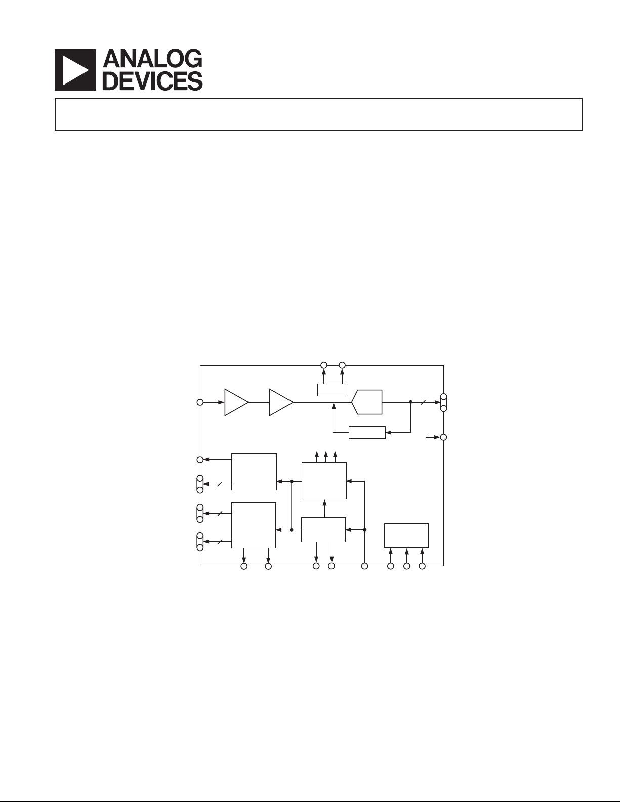
FUNCTIONAL BLOCK DIAGRAM
RS
H1 A–D
H2 A, B
V1 A/B
V3 A/B
TG1A
TG1B
TG3A
TG3B
AD9937
6
V2
V4
4
4
CDS
HORIZONTAL
DRIVERS
V- H
CONTROL
6dB TO 40dB
VGA
INTERNAL CLOCKS
PRECISION
GENERATOR
GENERATOR
GENERAL DESCRIPTION
The AD9937 is a highly integrated CCD signal processor. It
includes a complete analog front end with A/D conversion,
combined with a full-function programmable timing generator.
A Precision Timing core allows adjustment of high speed clocks
with 1.7 ns resolution at 12 MHz operation.
The AD9937 is specified at pixel rates of up to 12 MHz. The
analog front end includes black level clamping, CDS, VGA, and
a 10-bit A/D converter. The timing generator provides all the
necessary CCD clocks: RS, H-clocks, V-clocks, sensor gate pulses,
and substrate charge reset pulse. Operation is programmed using a
3-wire serial interface.
The AD9937 is packaged in a 56-lead LFCSP and specified over
an operating temperature range of –25°C to +85°C.
REFT REFB
VREF
ADC
CLAMP
TIMING
SYNC
INTERNAL
REGISTERS
10
DOUT
VCLK
LM OFD HD VD
REV. 0
Information furnished by Analog Devices is believed to be accurate and
reliable. However, no responsibility is assumed by Analog Devices for its
use, nor for any infringements of patents or other rights of third parties that
may result from its use. No license is granted by implication or otherwise
under any patent or patent rights of Analog Devices. Trademarks and
registered trademarks are the property of their respective companies.
VCKM
SLD SCK SDA
One Technology Way, P.O. Box 9106, Norwood, MA 02062-9106, U.S.A.
Tel: 781/329-4700 www.analog.com
Fax: 781/326-8703 © 2003 Analog Devices, Inc. All rights reserved.
Page 2

AD9937
TABLE OF CONTENTS
FEATURES . . . . . . . . . . . . . . . . . . . . . . . . . . . . . . . . . . . . . 1
APPLICATIONS . . . . . . . . . . . . . . . . . . . . . . . . . . . . . . . . . 1
GENERAL DESCRIPTION . . . . . . . . . . . . . . . . . . . . . . . . . 1
FUNCTIONAL BLOCK DIAGRAM . . . . . . . . . . . . . . . . . 1
SPECIFICATIONS . . . . . . . . . . . . . . . . . . . . . . . . . . . . . . . 3
DIGITAL SPECIFICATIONS . . . . . . . . . . . . . . . . . . . . . . . 3
ANALOG SPECIFICATIONS . . . . . . . . . . . . . . . . . . . . . . . 4
TIMING SPECIFICATIONS . . . . . . . . . . . . . . . . . . . . . . . 5
ABSOLUTION MAXIMUM RATINGS . . . . . . . . . . . . . . . 5
PACKAGE THERMAL CHARACTERISTICS . . . . . . . . . 5
ORDERING GUIDE . . . . . . . . . . . . . . . . . . . . . . . . . . . . . . 5
PIN CONFIGURATION . . . . . . . . . . . . . . . . . . . . . . . . . . . 6
PIN FUNCTION DESCRIPTIONS . . . . . . . . . . . . . . . . . . 6
TERMINOLOGY . . . . . . . . . . . . . . . . . . . . . . . . . . . . . . . . . 7
Differential Nonlinearity . . . . . . . . . . . . . . . . . . . . . . . . . . 7
Peak Nonlinearity . . . . . . . . . . . . . . . . . . . . . . . . . . . . . . . . 7
Total Output Noise . . . . . . . . . . . . . . . . . . . . . . . . . . . . . . 7
Power Supply Rejection . . . . . . . . . . . . . . . . . . . . . . . . . . . 7
EQUIVALENT CIRCUITS . . . . . . . . . . . . . . . . . . . . . . . . . 7
TYPICAL PERFORMANCE CHARACTERISTICS . . . . . 8
REGISTER MAPS . . . . . . . . . . . . . . . . . . . . . . . . . . . . . . . . 9
SERIAL INTERFACE TIMING . . . . . . . . . . . . . . . . . . . . 18
Control Register Serial Interface . . . . . . . . . . . . . . . . . . . 18
System and Mode Register Serial Interface . . . . . . . . . . . 18
Page/Burst Option . . . . . . . . . . . . . . . . . . . . . . . . . . . . . . 18
Random Access Option . . . . . . . . . . . . . . . . . . . . . . . . . . 18
Internal Power-On Reset Circuitry . . . . . . . . . . . . . . . . . . 19
VD Synchronous and Asynchronous Register Operation . 19
Asynchronous Register Operation . . . . . . . . . . . . . . . . . . 19
VD Synchronous Register Operation . . . . . . . . . . . . . . . . 19
SYSTEM OVERVIEW . . . . . . . . . . . . . . . . . . . . . . . . . . . . 20
ANALOG FRONT END DESCRIPTION AND
OPERATION . . . . . . . . . . . . . . . . . . . . . . . . . . . . . . . . . . . 21
DC Restore . . . . . . . . . . . . . . . . . . . . . . . . . . . . . . . . . . . 21
Correlated Double Sampler . . . . . . . . . . . . . . . . . . . . . . . 21
PRECISION TIMING HIGH SPEED TIMING
GENERATION . . . . . . . . . . . . . . . . . . . . . . . . . . . . . . . . . 22
Timing Resolution . . . . . . . . . . . . . . . . . . . . . . . . . . . . . . 22
High Speed Clock Programmability . . . . . . . . . . . . . . . . . 22
H-Driver and RS Outputs . . . . . . . . . . . . . . . . . . . . . . . . 22
MASTER AND SLAVE MODE OPERATION . . . . . . . . . 25
HORIZONTAL AND VERTICAL TIMING . . . . . . . . . . . 25
Individual HMASK Sequence . . . . . . . . . . . . . . . . . . . . . 25
Individual PBLK Sequences . . . . . . . . . . . . . . . . . . . . . . 25
Controlling CLPOB Clamp Pulse Timing . . . . . . . . . . . . 28
Vertical Sensor Transfer Gate Timing . . . . . . . . . . . . . . . 29
SHUTTER TIMING CONTROL . . . . . . . . . . . . . . . . . . . 29
Normal Shutter Mode . . . . . . . . . . . . . . . . . . . . . . . . . . . 29
High Precision Shutter Mode . . . . . . . . . . . . . . . . . . . . . . 29
Controlling LM Pulse Timing . . . . . . . . . . . . . . . . . . . . . 31
SPECIAL HORIZONTAL PATTERN TIMING . . . . . . . . 32
MASKING H1 AND H2 OUTPUTS . . . . . . . . . . . . . . . . . 33
Horizontal Masking . . . . . . . . . . . . . . . . . . . . . . . . . . . . . 33
Vertical Masking . . . . . . . . . . . . . . . . . . . . . . . . . . . . . . . 33
VERTICAL TIMING GENERATION . . . . . . . . . . . . . . . 35
CCD REGIONS . . . . . . . . . . . . . . . . . . . . . . . . . . . . . . . . . 35
POWER-UP . . . . . . . . . . . . . . . . . . . . . . . . . . . . . . . . . . . . 39
STANDBY SEQUENCE . . . . . . . . . . . . . . . . . . . . . . . . . . 40
POWER-DOWN SEQUENCE . . . . . . . . . . . . . . . . . . . . . . 41
CIRCUIT LAYOUT INFORMATION . . . . . . . . . . . . . . . 42
OUTLINE DIMENSIONS . . . . . . . . . . . . . . . . . . . . . . . . . 44
TABLES
Table I. Control Register Map . . . . . . . . . . . . . . . . . . . . . . . . 9
Table II. VTP Sequence System Register Map . . . . . . . . . . 10
Table III. H/LM System Register Map . . . . . . . . . . . . . . . . 12
Table IV. Shutter System Register Map . . . . . . . . . . . . . . . . 13
Table V. Mode_A . . . . . . . . . . . . . . . . . . . . . . . . . . . . . . . . 14
Table VI. Mode_B . . . . . . . . . . . . . . . . . . . . . . . . . . . . . . . . 16
Table VII. Serial Interface Registers . . . . . . . . . . . . . . . . . . 18
Table VIII. RS, H1, SHP, SHD, and DOUTPHASE
Timing Parameters . . . . . . . . . . . . . . . . . . . . . . . . . . . . . . 23
Table IX. Precision Timing Edge Locations for RS, H1,
SHP, SHD, and DOUTPHASE . . . . . . . . . . . . . . . . . . . . . 23
Table X. HD and VD Registers . . . . . . . . . . . . . . . . . . . . . . 25
Table XI. PBLK Registers . . . . . . . . . . . . . . . . . . . . . . . . . . 26
Table XII. CLPOB Registers . . . . . . . . . . . . . . . . . . . . . . . . 28
Table XIII. TG Registers . . . . . . . . . . . . . . . . . . . . . . . . . . . 29
Table XIV. OFD Registers . . . . . . . . . . . . . . . . . . . . . . . . . 30
Table XV. LM Registers . . . . . . . . . . . . . . . . . . . . . . . . . . . 31
Table XVI. Special H Pattern Registers . . . . . . . . . . . . . . . . 33
Table XVII. Sequence Change Positions Registers . . . . . . . 35
Table XVIII. Start-Up Polarities . . . . . . . . . . . . . . . . . . . . . 39
REV. 0–2–
Page 3
AD9937–SPECIFICATIONS
Parameter Min Typ Max Unit
TEMPERATURE RANGE
Operating –25 +85 °C
Storage –65 +150 °C
POWER SUPPLY VOLTAGE
AVDD (AFE Analog Supply) 2.7 3.0 3.6 V
TCVDD (Timing Core Analog Supply) 2.7 3.0 3.6 V
RSVDD (RS Driver) 2.7 3.0 3.6 V
HVDD1 (H1A, H2A, and H1C Drivers) 2.7 3.0 3.6 V
HVDD2 (H1B, H2B, and H1D Drivers) 2.7 3.0 3.6 V
DRVDD (Data Output Drivers) 2.7 3.0 3.6 V
DVDD (Digital) 2.7 3.0 3.6 V
POWER CONSUMPTION @ 10 MHz
Power from (AVDD + TCVDD + DRVDD + DVDD) 100 mW
Power from (HVDD1 + HVDD2)
Power from (RSVDD)
2
Standby Mode (AFE_STBY and DIG_STBY = 0) 1.5 mW
VCKM MAX CLOCK RATE 12 MHz
NOTES
H1A H2A H1B H2B H1C H1D
30 30 30 30 30 30
1
25 mW
3mW
10pF 10pF 10pF 10pF 10pF 10pF 10pF
30pF 50pF 30pF 50pF 30pF 30pF
10pF
1
H1 (A–D) and H2 (A, B) Loads
DIGITAL SPECIFICATIONS
(RSVDD = HVDD = 2.7 V to 3.6 V, –25C to +85C, unless otherwise noted.)
RS
30
10pF
2
RS Load
Parameter Symbol Min Typ Max Unit
LOGIC INPUTS (VCKM, SLD, SDA, and SCK)
High Level Input Voltage V
Low Level Input Voltage V
High Level Input Current I
Low Level Input Current I
Input Capacitance C
IH
IL
IH
IL
IN
2.1 V
0.6 V
40 µA
40 µA
10 pF
LOGIC OUTPUTS (Except H1(A–D), H2(A, B), and RS)
High Level Output Voltage @ IOH = 2 mA V
Low Level Output Voltage @ IOL = 2 mA V
OH
OL
DRVDD – 0.5 V
0.5 V
H-DRIVER OUTPUTS (H1(A–D), H2(A, B))
High Level Output Voltage @ Max Current V
Low Level Output Voltage @ Max Current V
OH
OL
DVDD – 0.5 V
0.5 V
H1(A–D) Maximum Output Current (Programmable) 12.25 mA
H2(A, B) Maximum Output Current (Programmable) 12.25 mA
Maximum Load Current 100 pF
RS-DRIVER OUTPUTS
High Level Output Voltage @ Max Current V
Low Level Output Voltage @ Max Current V
OH
OL
RSVDD – 0.5 V
0.5 V
RS Maximum Output Current (Programmable) 12.25 mA
Maximum Load Current 100 pF
Specifications subject to change without notice.
REV. 0 –3–
Page 4
AD9937
ANALOG SPECIFICATIONS
(AVDD = 3 V, f
= 12 MHz, –25C to +85C, unless otherwise noted.)
CLI
Parameter Min Typ Max Unit Notes
CDS
Allowable CCD Reset Transient 500 mV Input signal characteristics.*
Max Input Range before Saturation 1.0 V p-p
Max CCD Black Pixel Amplitude ±100 mV
VARIABLE GAIN AMPLIFIER (VGA)
Max Output Range 2.0 V p-p
Gain Control Resolution 10 Bits
Gain Monotonicity Guaranteed
Gain Range
Low Gain (VGA Code 0) 5.3 dB
Max Gain (VGA Code 1023) 40 41.1 dB
BLACK LEVEL CLAMP
Clamp Level Resolution 255 Steps
Clamp Level LSB measured at ADC output.
Min Clamp Level 0 LSB
Max Clamp Level 63.75 LSB
A/D CONVERTER
Resolution 10 Bits
Differential Nonlinearity (DNL) ± 0.4 ± 1.0 LSB
No Missing Codes Guaranteed
Full-Scale Input Voltage 2.0 V
VOLTAGE REFERENCE
Reference Top Voltage (REFT) 2.0 V
Reference Bottom Voltage (REFB) 1.0 V
SYSTEM PERFORMANCE Includes entire signal chain.
Gain Accuracy
Low Gain (VGA Code 17) 5 6 7 dB Gain = (0.035 × Code) + 5.4 dB
Max Gain (VGA Code 1023) 40.2 41.2 42.2 dB
Peak Nonlinearity, 500 mV Input Signal 0.1 % 12 dB gain applied.
Total Output Noise 0.3 LSB rms AC ground input, 6 dB gain applied.
Power Supply Rejection (PSR) 40 dB Measured with step change on supply.
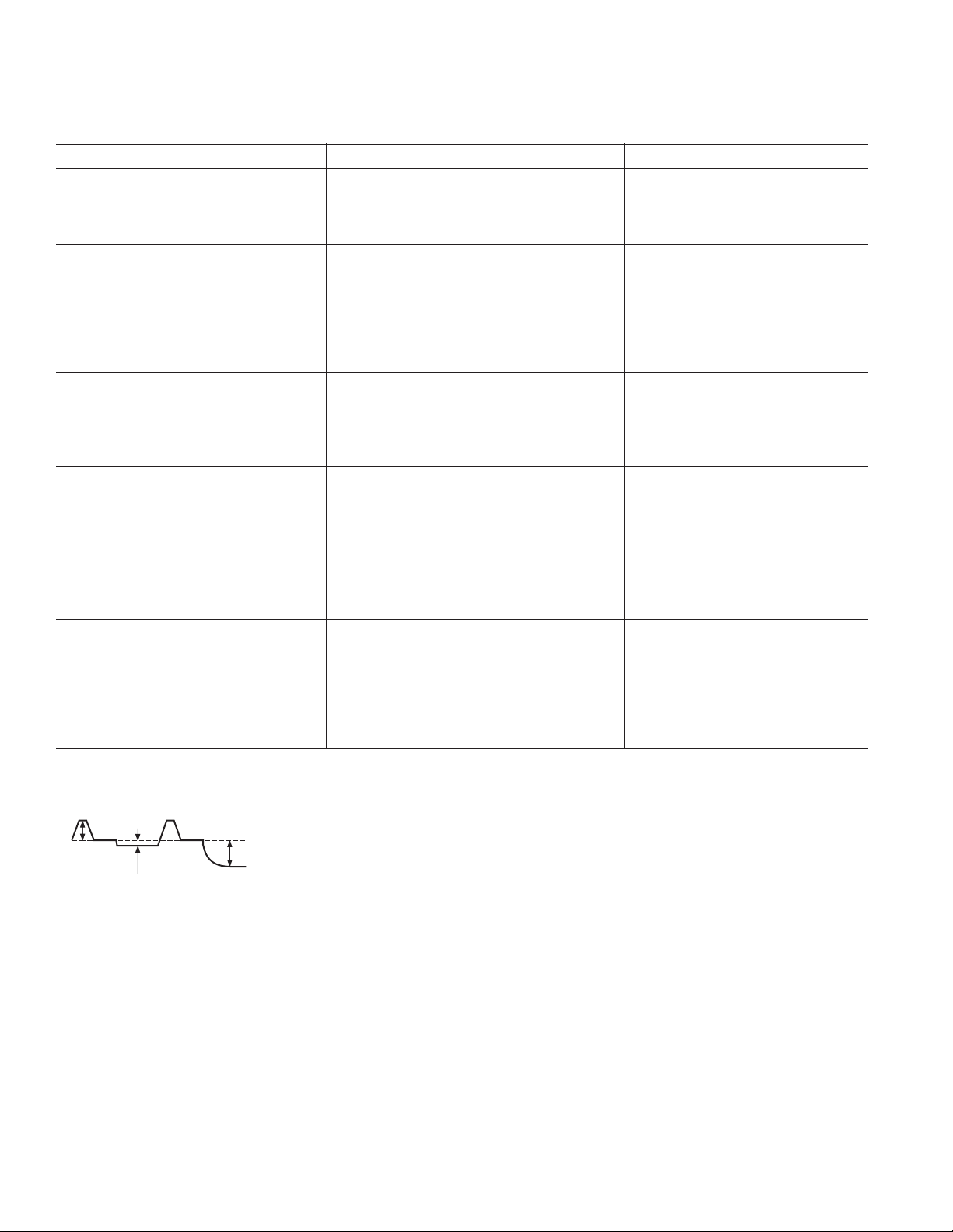
*Input signal characteristics defined as follows:
500mV TYP
RESET
TRANSIENT
100mV MAX
OPTICAL
BLACK PI XEL
Specifications subject to change without notice.
1V MAX
INPUT
SIGNAL RANGE
REV. 0–4–
Page 5
AD9937
TIMING SPECIFICATIONS
(CL = 20 pF, AVDD = DVDD = DRVDD = 3 V, f
= 12 MHz, unless otherwise noted.)
CLI
Parameter Symbol Min Typ Max Unit
MASTER CLOCK, VCKM
VCKM Clock Period t
CONV
83.33 ns
VCKM High/Low Pulsewidth 41.67 ns
Delay from VCKM Rising Edge to Internal Pixel Position 0 t
AFE CLAMP PULSES
CLPOB Pulsewidth
AFE SAMPLE LOCATION
1
2
1
(See Figure 13)
SHP Sample Edge to SHD Sample Edge t
VCKMDLY
S1
220Pixels
33.34 41.67 ns
9ns
DATA OUTPUTS
Output Delay from VCLK Rising Edge t
OD
9ns
Pipeline Delay from SHP/SHD Sampling (See Figure 40) 9 Cycles
SERIAL INTERFACE
Maximum SCK Frequency f
SLD to SCK Setup Time t
SCK to SLD Hold Time t
SDA Valid to SCK Rising Edge Setup t
SCK Falling Edge to SDA Valid Hold t
SCK Falling Edge to SDA Valid Read t
NOTES
1
Parameter is programmable.
2
Minimum CLPOB pulsewidth is for functional operation only. Wider typical pulses are recommended to achieve good clamp performance.
Specifications subject to change without notice.
SCLK
LS
LH
DS
DH
DV
10 MHz
10 ns
10 ns
10 ns
10 ns
10 ns
ABSOLUTE MAXIMUM RATINGS
With
Respect
PACKAGE THERMAL CHARACTERISTICS
Thermal Resistance
JA = 24.9°C/W
Parameter To Min Max Unit
AVDD AVSS –0.3 +3.9 V
TCVDD TCVSS –0.3 +3.9 V
ORDERING GUIDE
HVDD HVSS –0.3 +3.9 V
RSVDD RSVSS –0.3 +3.9 V
DVDD DVSS –0.3 +3.9 V
DRVDD DRVSS –0.3 +3.9 V
Model Range Description Option
AD9937KCP –25°C to +85°CLead Frame CP-56
Temperature Package Package
RS Output RSVSS –0.3 RSVDD + 0.3 V
H1(A–D), H2(A, B)Output HVSS –0.3 HVDD + 0.3 V
Digital Outputs DVSS –0.3 DVDD + 0.3 V
Digital Inputs DVSS –0.3 DVDD + 0.3 V
AD9937KCPRL –25°C to +85°CLead Frame CP-56
SCK, SLD, SDA DVSS –0.3 DVDD + 0.3 V
VRT, VRB AVSS –0.3 AVDD + 0.3 V
CCDIN AVSS –0.3 AVDD + 0.3 V
Junction Temperature 150 °C
Lead Temperature, 10 sec 350 °C
CAUTION
ESD (electrostatic discharge) sensitive device. Electrostatic charges as high as 4000 V readily
accumulate on the human body and test equipment and can discharge without detection. Although the
AD9937 features proprietary ESD protection circuitry, permanent damage may occur on devices
subjected to high energy electrostatic discharges. Therefore, proper ESD precautions are recommended
to avoid performance degradation or loss of functionality.
Chip Scale
Package
(LFCSP)
Chip Scale
Package
(LFCSP)
REV. 0
–5–
Page 6
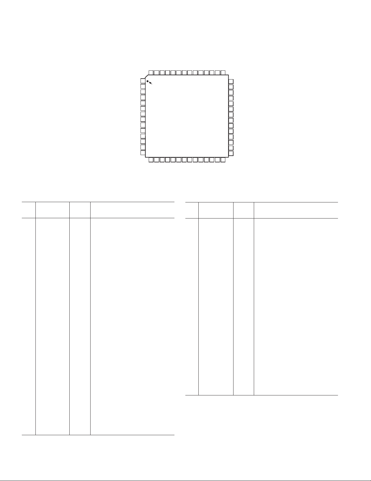
AD9937
NC
NC
D0
D1
D2
D3
DRVSS
DRVDD
D4
D5
D6
D7
D8
D9
NC = NO CONNECT
PIN CONFIGURATION
SCK
SLD
SDA
VDHDOFD
DVSS
DVD DLMV4
4950515253545556
1
PIN 1
2
IDENTIFIER
3
4
5
6
7
8
9
10
11
12
13
14
VCLK
HVDD2
H1D
HVSS2
AD9937
TOP VIEW
(Not to Scale)
H2B
H1B
HVDD1
HVSS1
TG3B
V3A/B
H2A
H1A
TG3A
RS
RSVSS
48 47 46 45 44 43
H1C
V2
2827262515 16 17 18 19 20 21 22 23 24
RSVDD
42
41
40
39
38
37
36
35
34
33
32
31
30
29
TG1B
V1A/B
TG1A
REFB
REFT
AVSS
CCDIN
AV DD
VCKM
TCVDD
TCVSS
NC
NC
NC
PIN FUNCTION DESCRIPTIONS
Pin
No. Mnemonic Type2Description
1NCNCNo Connect
2NCNCNo Connect
3D0DOData Output
4D1DOData Output
5D2DOData Output
6D3DOData Output
7 DRVSS P Data Output Driver Ground
8 DRVDD P Data Output Driver Supply
9D4DOData Output
10 D5 DO Data Output
11 D6 DO Data Output
12 D7 DO Data Output
13 D8 DO Data Output
14 D9 DO Data Output
15 VCLK DO Data Output Clock
16 HVDD2 P Horizontal Driver Supply 2
for H1D, H2B, and H1B
17 HVSS2 P Horizontal Driver Ground 2
18 H1D DO CCD Horizontal Clock 4
19 H2B DO CCD Horizontal Clock 6
20 H1B DO CCD Horizontal Clock 2
21 HVDD1 P Horizontal Driver Supply 1
for H1C, H2A, and H1A
22 HVSS1 P Horizontal Driver Ground 1
23 H1C DO CCD Horizontal Clock 3
24 H2A DO CCD Horizontal Clock 5
25 H1A DO CCD Horizontal Clock 1
26 RSVSS P RS Driver Ground
27 RS DO CCD Reset Gate Clock
28 RSVDD P RS Driver Supply
29 NC NC No Connect
30 NC NC No Connect
1
Pin
No. Mnemonic Type2Description
31 NC NC No Connect
32 TCVSS P Analog Ground for Timing Core
33 TCVDD P Analog Supply for Timing Core
34 VCKM DI
3
Reference Clock Input
35 AVDD P Analog Supply for AFE
36 CCDIN AI CCD Input Signal
37 AVSS P Analog Ground for AFE
38 REFT AO Voltage Reference Top Bypass
39 REFB AO Voltage Reference Bottom Bypass
40 TG1A DO CCD Sensor Gate Pulse 1
41 V1A/B DO CCD Vertical Transfer Clock 1
42 TG1B DO CCD Sensor Gate Pulse 2
43 V2 DO CCD Vertical Transfer Clock 2
44 TG3A DO CCD Sensor Gate Pulse 3
45 V3A/B DO CCD Vertical Transfer Clock 3
46 TG3B DO CCD Sensor Gate Pulse 4
47 V4 DO CCD Vertical Transfer Clock 4
48 LM DO Line Memory Control Pulse
49 DVDD P Digital Supply
50 DVSS P Digital Ground
51 OFD DO CCD Substrate Reset Pulse
52 HD DO Horizontal Sync Pulse
53 VD DO Vertical Sync Pulse
54 SLD DI
55 SDA DI
56 SCK DI
NOTES
1
See Figure 41 for circuit configuration.
2
AI = Analog Input, AO = Analog Output, DI = Digital Input,
DO = Digital Output, DIO = Digital Input/Output, P = Power,
NC = No Connection.
3
Schmitt trigger type input.
3
3-Wire Serial Load Pulse
3
3-Wire Serial Data
3
3-Wire Serial Clock
REV. 0–6–
Page 7
AD9937
TERMINOLOGY
Differential Nonlinearity (DNL)
An ideal ADC exhibits code transitions that are exactly 1 LSB
apart. DNL is the deviation from this ideal value. Thus, every
code must have a finite width. No missing codes guaranteed to
10-bit resolution indicates that all 1024 codes must be present
over all operating conditions.
Peak Nonlinearity
Peak nonlinearity, a full signal chain specification, refers to the
peak deviation of the output of the AD9937 from a true straight
line. The point used as zero scale occurs 1/2 LSB before the first
code transition. Positive full scale is defined as a level 1 1/2 LSB
beyond the last code transition. The deviation is measured from
the middle of each particular output code to the true straight line.
The error is then expressed as a percentage of the 2 V ADC fullscale signal. The input signal is always appropriately gained up
to fill the ADC’s full-scale range.
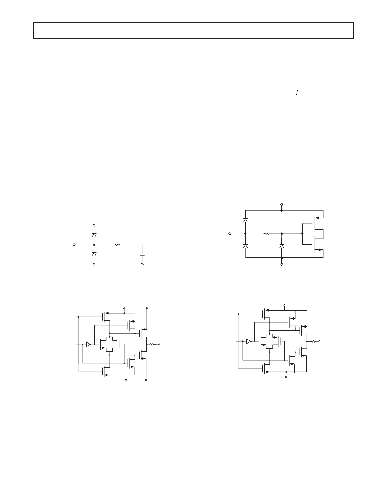
EQUIVALENT CIRCUITS
AVDD
Total Output Noise
The rms output noise is measured using histogram techniques.
The standard deviation of the ADC output codes is calculated
in LSB and represents the rms noise level of the total signal
chain at the specified gain setting. The output noise can be
converted to an equivalent voltage, using the relationship
12LSB ADC Full Scale codes
=
()
N
where N is the bit resolution of the ADC. For the AD9937, 1 LSB
is 1.95 mV.
Power Supply Rejection (PSR)
The PSR is measured with a step change applied to the supply
pins. This represents a very high frequency disturbance on the
AD9937’s power supply. The PSR specification is calculated
from the change in the data outputs for a given step change in
the supply voltage.
DVDD
330
DATA
TRISTATEOUT
R
AVSS
AVSS
Figure 1. CCDIN
DVDD
DVSS
DRVDD
DRVSS
Figure 2. Digital Data Outputs
DOUT
DVSS
Figure 3. Digital Inputs
HVDD1, HVDD2,
OR RSVDD
RS,
H1 (A–D),
H2 (A, B)
ENABLE
HVSS1, HVSS2,
OR RSVSS
OUTPUT
Figure 4. H1(A–D), H2(A, B), and RS Drivers
REV. 0
–7–
Page 8
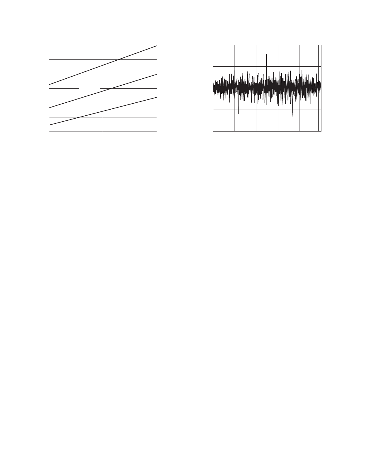
AD9937–Typical Performance Characteristics
0
160
150
140
130
120
POWER DISSIPATION – mW
110
100
81210
VDD = 3.3V
VDD = 3.0V
VDD = 2.7V
TPC 1. Power vs. Sample Rate
SAMPLE RATE – MHz
0.50
0.25
0
DNL – LSB
–0.25
–0.50
0 200
VDD = 3.0V
400 600 800 100
CODE
TPC 2. Typical DNL Performance
REV. 0–8–
Page 9

AD9937
Table I. Control Register Map
Bit Bit Register
Addr Breakdown Width Default Name Function
0 (23:0) 24 0 SW_RESET Software Reset = 000000 (Reset All Registers to Default).
10 10 OUTCONT_REG Internal OUTCONT Signal Control (0 = Digital Outputs held
at fixed dc level, 1 = Normal Operation).
(23:1) 23 Unused
2(1:0) 2 0 AFE_STBY AFE Standby (0 = Full Standby, 1 = Normal Operation,
2/3 = Reference Standby).
210DIG_STBY Digital Standby (0 = Full Standby, 1 = Normal Operation).
(23:3) 21 Unused
3(7:0) 8 0x80 REFBLACK Black Clamp Level.
811BC_EN 1 = Black Clamp Enable.
910TESTMODE This register should always be set to 0.
10 1 0 TESTMODE This register should always be set to 0.
11 1 0 PBLK_LEVEL 0 = Blank to 0, 1 = Blank to Clamp Level (REFBLACK).
12 1 0 TRISTATEOUT 0 = Data Outputs are Driven, 1 = Data Outputs are Three-Stated.
13 10 RETIMEOUT_BAR 0 = Retime Data Outputs, 1 = Do Not Retime Data Outputs.
14 1 0 GRAY_ENCODE 1 = Gray Encode ADC Outputs.
(16:15) 2 0 TESTMODE This register should always be set to 0.
17 1 0 TESTMODE This register should always be set to 0.
18 1 1 TESTMODE This register should always be set to 1.
(23:19) 5 Unused
40 10 VCKM_DIVIDE VCKM Input Clock Divider (0 = VCKM, 1 = VCKM/2).
110H1BLKRETIME Retimes the H1 HBLK to Internal Clock.
210LM_INVERT LM Inversion Control (1 = Invert Programmed LM).
310TGOFD_INVERT TG and OFD Inversion Control (1 = Invert Programmed TG
and ODF).
410VDHD_INVERT VD and HD Inversion Control (1 = Invert Programmed VD
and HD; Note that Internal VD/HD Are HI Active).
510MASTER Operating Mode (0 = Slave Mode, 1 = Master Mode).
(23:6) 18 Unused
5(5:0) 6 0x00 SHDLOC SHD Sample Location.
(11:6) 6 0x24 SHPLOC SHP Sample Location.
(17:12) 6 0x00 DOUTPHASE Data Output [9:0] and VCLK Phase Adjustment.
(19:18) 2 0x00 DOUT_DELAY Data Output Clock Selection (0 = No Delay, 1 = ~4 ns, 2 = ~8 ns,
3 = ~12 ns).
20 1 0 VCLKMASK VCLK Masking Control (1 = Mask).
21 1 1 VCLK_INVERT 1 = Invert VCLK.
22 1 0 DTEST 1 = Internal Digital Signal Test Mode.
23 1 – Unused
6(5:0) 6 0x00 H1POSLOC H1 Positive Edge Location.
(11:6) 6 0x20 H1NEGLOC H1 Negative Edge Location.
(17:12) 6 0x00 RSPOSLOC RS Positive Edge Location.
(23:18) 6 0x10 RSNEGLOC RS Negative Edge Location.
7(2:0) 3 4 H1DRV H1A/B/C/D Drive Strength (0 = OFF, 1 = 1.75 mA, 2 = 3.5 mA,
3 = 5.25 mA, 4 = 7 mA, 5 = 8.75 mA, 6 = 10.5 mA, 7 = 12.25 mA).
(5:3) 3 4 H2DRV H2A/B Drive Strength (see H1DRV).
(8:6) 3 4 RSDRV RS Drive Strength (see H1DRV).
(23:9) 15 Unused
(23:1) 23 Unused
REV. 0
–9–
Page 10

AD9937
Table I. Control Register Map (continued)
Bit Bit Register
Addr Breakdown Width Default Name Function
80 10 MODE Mode Control Bit. (0 = Mode A, 1 = Mode B)
(23:1) 23 Unused
90 11 SPEN Single Pulse (SP) Output Enable.
(4:1) 4 0x9 SPLOGIC Single Pulse Logic Setting (0 = OR, 1 = AND).
(23:5) 19 Unused
10 0 1 1 OFDEN OFD Output Enable Control (0 = Disable, 1 = Enable).
(11:1) 11 0x7FF OFDNUM Total Number of OFD Pulses per Field.
12 1 1 TGEN TG Output Enable Control (0 = Disable, 1 = Enable).
(23:13) 11 Unused
11 (11:0) 12 4095 OFDHPTOG1 High Precision OFD Toggle Position 1.
(23:12) 12 4095 OFDHPTOG2 High Precision OFD Toggle Position 2.
12 (9:0) 10 0x000 VGAGAIN VGA Gain Control.
(23:10) 14 Unused
Denotes VD synchronous registers (control addresses 8, 9, 10, 11, and 12).
Table II. VTP Sequence System Register Map (Addr 0x14)
Bit Bit Register
Addr Breakdown Width Default Name Function
VTP_Reg(0) (11:0) 12 ENDADDRESS Sub Word End Address
(23:12) 12 STARTADDRESS Sub Word Start Address
(31:24) 8 VTP_Reg_Addr System Register Address 0x14
VTP_Reg(1) (8:0) 9 279 VTPLEN_0 VTP0: Length between Repetitions
(17:9) 9 75 V1TOG1_0 VTP0: V1 Toggle Position 1
(26:18) 9 250 V1TOG2_0 VTP0: V1 Toggle Position 2
27 1 1 V1POL_0 VTP0: V1 Start Polarity
28 1 0 V2POL_0 VTP0: V2 Start Polarity
29 1 0 V3POL_0 VTP0: V3 Start Polarity
30 1 1 V4POL_0 VTP0: V4 Start Polarity
31 1 Unused
VTP_Reg(2) (8:0) 9 40 V2TOG1_0 VTP0: V2 Toggle Position 1
(17:9) 9 145 V2TOG2_0 VTP0: V2 Toggle Position 2
(26:18) 9 110 V3TOG1_0 VTP0: V3 Toggle Position 1
(31:27) 5 Unused
VTP_Reg(3) (8:0) 9 215 V3TOG2_0 VTP0: V3 Toggle Position 2
(17:9) 9 5 V4TOG1_0 VTP0: V4 Toggle Position 1
(26:18) 9 180 V4TOG2_0 VTP0: V4 Toggle Position 2
(31:27) 5 Unused
VTP_Reg(4) (8:0) 9 99 VTPLEN_1 VTP1: Length between Repetitions
(17:9) 9 29 V1TOG1_1 VTP1: V1 Toggle Position 1
(26:18) 9 99 V1TOG2_1 VTP1: V1 Toggle Position 2
27 1 1 V1POL_1 VTP1: V1 Start Polarity
28 1 0 V2POL_1 VTP1: V2 Start Polarity
29 1 0 V3POL_1 VTP1: V3 Start Polarity
30 1 1 V4POL_1 VTP1: V4 Start Polarity
31 1 Unused
VTP_Reg(5) (8:0) 9 15 V2TOG1_1 VTP1: V2 Toggle Position 1
(17:9) 9 57 V2TOG2_1 VTP1: V2 Toggle Position 2
(26:18) 9 43 V3TOG1_1 VTP1: V3 Toggle Position 1
(31:27) 5 Unused
REV. 0–10–
Page 11

AD9937
Table II. VTP Sequence System Register Map (Addr 0x14) (continued)
Bit Bit Register
Addr Breakdown Width Default Name Function
VTP_Reg(6) (8:0) 9 85 V3TOG2_1 VTP1: V3 Toggle Position 2
(17:9) 9 1 V4TOG1_1 VTP1: V4 Toggle Position 1
(26:18) 9 71 V4TOG2_1 VTP1: V4 Toggle Position 2
(31:27) 5 Unused
VTP_Reg(7) (8:0) 9 99 VTPLEN_2 VTP2: Length between Repetitions
(17:9) 9 29 V1TOG1_2 VTP2: V1 Toggle Position 1
(26:18) 9 99 V1TOG2_2 VTP2: V1 Toggle Position 2
27 1 1 V1POL_2 VTP2: V1 Start Polarity
28 1 0 V2POL_2 VTP2: V2 Start Polarity
29 1 0 V3POL_2 VTP2: V3 Start Polarity
30 1 1 V4POL_2 VTP2: V4 Start Polarity
31 1 Unused
VTP_Reg(8) (8:0) 9 15 V2TOG1_2 VTP2: V2 Toggle Position 1
(17:9) 9 57 V2TOG2_2 VTP2: V2 Toggle Position 2
(26:18) 9 43 V3TOG1_2 VTP2: V3 Toggle Position 1
(31:27) 5 Unused
VTP_Reg(9) (8:0) 9 85 V3TOG2_2 VTP2: V3 Toggle Position 2
(17:9) 9 1 V4TOG1_2 VTP2: V4 Toggle Position 1
(26:18) 9 71 V4TOG2_2 VTP2: V4 Toggle Position 2
(31:27) 5 Unused
VTP_Reg(10) (11:0) 12 40 SP1TOG1 SP1 Toggle Position 1 (V1A/V1B)
(23:12) 12 410 SP1TOG2 SP1 Toggle Position 2 (V1A/V1B)
(31:24) 8 Unused
VTP_Reg(11) (11:0) 12 490 SP2TOG1 SP2 Toggle Position 1 (V2)
(23:12) 12 780 SP2TOG2 SP2 Toggle Position 2 (V2)
(31:24) 8 Unused
VTP_Reg(12) (11:0) 12 80 SP3TOG1 SP3 Toggle Position 1 (V3A/V3B)
(23:12) 12 360 SP3TOG2 SP3 Toggle Position 2 (V3A/V3B)
(31:24) 8 Unused
VTP_Reg(13) (11:0) 12 450 SP4TOG1 SP4 Toggle Position 1 (V4)
(23:12) 12 820 SP4TOG2 SP4 Toggle Position 2 (V4)
(31:24) 8 Unused
REV. 0
–11–
Page 12

AD9937
Table III. H/LM System Register Map (Addr 0x15)
Bit Bit Register
Addr Breakdown Width Default Name Function
HLM_Reg(0) (11:0) 12 ENDADDRESS Sub Word End Address
(23:12) 12 STARTADDRESS Sub Word Start Address
(31:24) 8 HLM_Reg_Addr System Register Address 0x15
HLM_Reg(1) 0 1 0 H1APOL H1A Special H-Pattern Start Polarity
110H1BPOL H1B Special H-Pattern Start Polarity
211H1CPOL H1C Special H-Pattern Start Polarity
311H1DPOL H1D Special H-Pattern Start Polarity
410H2APOL H2A Special H-Pattern Start Polarity
510H2BPOL H2B Special H-Pattern Start Polarity
(31:6) 26 Unused
HLM_Reg(2) (5:0) 6 0x00 SPH1A1 H1A Special H-Pattern during LM Repetition 1
(11:6) 6 0x04 SPH1B1 H1B Special H-Pattern during LM Repetition 1
(17:12) 6 0x01 SPH1C1 H1C Special H-Pattern during LM Repetition 1
(31:18) 14 Unused
HLM_Reg(3) (5:0) 6 0x07 SPH1D1 H1D Special H-Pattern during LM Repetition 1
(11:6) 6 0x08 SPH2A1 H2A Special H-Pattern during LM Repetition 1
(17:12) 6 0x22 SPH2B1 H2B Special H-Pattern during LM Repetition 1
(31:18) 14 Unused
HLM_Reg(4) (5:0) 6 0x34 SPH1A2 H1A Special H-Pattern during LM Repetition 2
(11:6) 6 0x34 SPH1B2 H1B Special H-Pattern during LM Repetition 2
(17:12) 6 0x04 SPH1C2 H1C Special H-Pattern during LM Repetition 2
(31:18) 14 Unused
HLM_Reg(5) (5:0) 6 0x04 SPH1D2 H1D Special H-Pattern during LM Repetition 2
(11:6) 6 0x3A SPH2A2 H2A Special H-Pattern during LM Repetition 2
(17:12) 6 0x0B SPH2B2 H2B Special H-Pattern during LM Repetition 2
(31:18) 14 Unused
HLM_Reg(6) (5:0) 6 0x3D SPH1A3 H1A Special H-Pattern during LM Repetition 3
(11:6) 6 0x3F SPH1B3 H1B Special H-Pattern during LM Repetition 3
(17:12) 6 0x3C SPH1C3 H1C Special H-Pattern during LM Repetition 3
(31:18) 14 Unused
HLM_Reg(7) (5:0) 6 0x3C SPH1D3 H1D Special H-Pattern during LM Repetition 3
(11:6) 6 0x03 SPH2A2 H2A Special H-Pattern during LM Repetition 3
(17:12) 6 0x02 SPH2B3 H2B Special H-Pattern during LM Repetition 3
(31:18) 14 Unused
HLM_Reg(8) (7:0) 8 99 LMLEN0 LM Pattern 0 (LM0): LM Counter Length
(15:8) 8 5 LMTOG1_0 LM Pattern 0 (LM0): Toggle Position 1
(23:16) 8 55 LMTOG2_0 LM Pattern 0 (LM0): Toggle Position 2
(31:24) 8 87 SPHSTART0 LM Pattern 0 (LM0): Special H Pulse Start Position
HLM_Reg(9) (7:0) 8 29 LMLEN1 LM Pattern 1 (LM1): LM Counter Length
(15:8) 8 2 LMTOG1_1 LM Pattern 1 (LM1): Toggle Position 1
(23:16) 8 26 LMTOG2_1 LM Pattern 1 (LM1): Toggle Position 2
(31:24) 8 0 SPHSTART1 LM Pattern 1 (LM1): Special H Pulse Start Position
REV. 0–12–
Page 13

Table IV. Shutter System Register Map (Addr 0x16)
Bit Bit Register
Addr Breakdown Width Default Name Function
Shut_Reg(0) (11:0) 12 ENDADDRESS Sub Word End Address
(23:12) 12 STARTADDRESS Sub Word Start Address
(31:24) 8 SHUT_Reg_Addr System Register Address 0x16
Shut_Reg(1) (11:0) 12 80 TGTOG1_0 TG0 Pulse Toggle Position 1
(23:12) 12 370 TGTOG2_0 TG0 Pulse Toggle Position 2
(31:24) 8 Unused
Shut_Reg(2) (11:0) 12 490 TGTOG1_1 TG1 Pulse Toggle Position 1
(23:12) 12 780 TGTOG2_1 TG1 Pulse Toggle Position 2
(31:24) 8 Unused
Shut_Reg(3) (11:0) 12 540 OFDTOG1_0 OFD0 Pulse Toggle Position 1
(23:12) 12 720 OFDTOG2_0 OFD0 Pulse Toggle Position 2
(31:24) 8 Unused
Shut_Reg(4) (11:0) 12 830 OFDTOG1_1 OFD1 Pulse Toggle Position 1
(23:12) 12 860 OFDTOG2_1 OFD1 Pulse Toggle Position 2
(31:24) 8 Unused
AD9937
REV. 0
–13–
Page 14

AD9937
Table V. Mode_A (Addr 0x17)
Bit Bit Register
Addr Breakdown Width Default Name Function
Mode_Reg(0) (11:0) 12 ENDADDRESS Sub Word End Address
(23:12) 12 STARTADDRESS Sub Word Start Address
(31:24) 8 MODE_Reg_Addr Mode Register Address (Mode A = Addr 0x17)
Mode_Reg(1) (6:0) 7 0 TGACTLINE TG Active Line
7 10TGPATSEL0 TG1A/B Pattern Selector (0 = TG0, 1 = TG1)
8 11TGPATSEL1 TG3A/B Pattern Selector (0 = TG0, 1 = TG1)
(12:9) 4 0xA TGMASK TG Masking Control (1 = Mask)
13 1 0 OFDPATSEL OFD Pattern Selection (0 = OFD0, 1 = OFD1)
(31:14) 18 Unused
Mode_Reg(2) (11:0) 12 831 HDTOG1 HD Toggle Position 1
(23:12) 12 866 HDTOG2 HD Toggle Position 2
(31:24) 8 Unused
Mode_Reg(3) (11:0) 12 4095 HDTOG3 HD Toggle Position 3
(23:12) 12 4095 HDTOG4 HD Toggle Position 4
(31:24) 8 Unused
Mode_Reg(4) (11:0) 12 2339 HDLASTLEN HD Last Line Length
(22:12) 11 262 VDLEN VD Field Length
(26:23) 4 0 VDTOG1 VD Toggle Position 1
(30:27) 4 4 VDTOG2 VD Toggle Position 2
31 1 Unused
Mode_Reg(5) (11:0) 12 1543 CLPOBTOG1 CLPOB Toggle Position 1
(23:12) 12 1557 CLPOBTOG2 CLPOB Toggle Position 2
(31:24) 8 Unused
Mode_Reg(6) (11:0) 12 4095 CLPOBTOG3 CLPOB Toggle Position 3
(23:12) 12 4095 CLPOBTOG4 CLPOB Toggle Position 4
(31:24) 8 Unused
Mode_Reg(7) (11:0) 12 0 HBLKTOG1 HBLK Toggle Position 1
(23:12) 12 869 HBLKTOG2 HBLK Toggle Position 2
24 1 0 H1TOG12POL H1 Polarity between Toggle Positions 1 and 2
(31:25) 7 Unused
Mode_Reg(8) (11:0) 12 4095 HBLKTOG3 HBLK Toggle Position 3
(23:12) 12 4095 HBLKTOG4 HBLK Toggle Position 4
24 1 0 H1TOG34POL H1 Polarity between Toggle Positions 3 and 4
(31:25) 7 Unused
Mode_Reg(9) (11:0) 12 6 PBLKTOG1 PBLK Toggle Position 1
(23:12) 12 878 PBLKTOG2 PBLK Toggle Position 2
(31:24) 8 Unused
Mode_Reg(10) (11:0) 12 4095 PBLKTOG3 PBLK Toggle Position 3
(23:12) 12 4095 PBLKTOG4 PBLK Toggle Position 4
(31:24) 8 Unused
Mode_Reg(11) (10:0) 11 255 PBLKSTART PBLK Start Position
(21:11) 11 3 PBLKSTOP PBLK Stop Position
(31:22) 10 Unused
Mode_Reg(12) (10:0) 11 0 HMASKSTART Vertical H Masking Start Position
(21:11) 11 1 HMASKSTOP Vertical H Masking Stop Position
22 1 0 H1MASKPOL Masking Polarity for H1 during Vertical Blanking Period
(31:23) 9 Unused
Mode_Reg(13) (11:0) 12 550 LMSTART0 LM Counter Start Position 1
(23:12) 12 4095 LMSTART1 LM Counter Start Position 2
(31:24) 8 Unused
REV. 0–14–
Page 15

AD9937
Table V. Mode_A (Addr 0x17) (continued)
Bit Bit Register
Addr Breakdown Width Default Name Function
Mode_Reg(14) (7:0) 8 1 SCP1 Sequence Change Position 1
(15:8) 8 0 SCP2 Sequence Change Position 2
(23:16) 8 0 SCP3 Sequence Change Position 3
(31:24) 8 0 SCP4 Sequence Change Position 4
Mode_Reg(15) (11:0) 12 1559 HDLEN0 HD Counter Length Value for Region 0
(13:12) 2 0 VTPPATSEL0 VTP Pattern Select (0 = VTP0, 1 = VTP1, 2 = VTP2)
(16:14) 3 0 VTPREP0 VTP Pulse Repetition Number in Region 0
17 1 0 LMPATSEL0 LM Pattern Select for Region 0 (0 = LM0, 1 = LM1)
(19:18) 2 0 LMREP0 LM Repetition Number in Region 0
20 1 0 SPHEN0 Special H-Pattern Enable in Region 0
21 1 1 CLPOBEN0 CLPOB Enable in Region 0
(31:22) 10 Unused
Mode_Reg(16) (11:0) 12 1559 HDLEN1 HD Counter Length Value for Region 1
(13:12) 2 0 VTPPATSEL1 VTP Pattern Select (0 = VTP0, 1 = VTP1, 2 = VTP2)
(16:14) 3 2 VTPREP1 VTP Pulse Repetition Number in Region 1
17 1 0 LMPATSEL1 LM Pattern Select for Region 1 (0 = LM0, 1 = LM1)
(19:18) 2 3 LMREP1 LM Repetition Number in Region 1
20 1 1 SPHEN1 Special H-Pattern Enable in Region 1
21 1 1 CLPOBEN1 CLPOB Enable in Region 1
(31:22) 10 Unused
Mode_Reg(17) (11:0) 12 1559 HDLEN2 HD Counter Length Value for Region 2
(13:12) 2 0 VTPPATSEL2 VTP Pattern Select (0 = VTP0, 1 = VTP1, 2 = VTP2)
(16:14) 3 2 VTPREP2 VTP Pulse Repetition Number in Region 2
17 1 0 LMPATSEL2 LM Pattern Select for Region 2 (0 = LM0, 1 = LM1)
(19:18) 2 3 LMREP2 LM Repetition Number in Region 2
20 1 1 SPHEN2 Special H-Pattern Enable in Region 2
21 1 1 CLPOBEN2 CLPOB Enable in Region 2
(31:22) 10 Unused
Mode_Reg(18) (11:0) 12 1559 HDLEN3 HD Counter Length Value for Region 3
(13:12) 2 0 VTPPATSEL3 VTP Pattern Select (0 = VTP0, 1 = VTP1, 2 = VTP2)
(16:14) 3 2 VTPREP3 VTP Pulse Repetition Number in Region 3
17 1 0 LMPATSEL3 LM Pattern Select for Region 3 (0 = LM0, 1 = LM1)
(19:18) 2 3 LMREP3 LM Repetition Number in Region 3
20 1 1 SPHEN3 Special H-Pattern Enable in Region 3
21 1 1 CLPOBEN3 CLPOB Enable in Region 3
(31:22) 10 Unused
Mode_Reg(19) (11:0) 12 1559 HDLEN4 HD Counter Length Value for Region 4
(13:12) 2 0 VTPPATSEL4 VTP Pattern Select (0 = VTP0, 1 = VTP1, 2 = VTP2)
(16:14) 3 2 VTPREP4 VTP Pulse Repetition Number in Region 4
17 1 0 LMPATSEL4 LM Pattern Select for Region 4 (0 = LM0, 1 = LM1)
(19:18) 2 3 LMREP4 LM Repetition Number in Region 4
20 1 1 SPHEN4 Special H-Pattern Enable in Region 4
21 1 1 CLPOBEN4 CLPOB Enable in Region 4
(31:22) 10 Unused
REV. 0
–15–
Page 16

AD9937
Table VI. Mode_B (Addr 0x18)
Bit Bit Register
Addr Breakdown Width Default Name Function
Mode_Reg(0) (11:0) 12 ENDADDRESS Sub Word End Address
(23:12) 12 STARTADDRESS Sub Word Start Address
(31:24) 8 MODE_Reg_Addr Mode Register Address (Mode B = Addr 0x18)
Mode_Reg(1) (6:0) 7 0 TGACTLINE TG Active Line
710TGPATSEL0 TG1A/B Pattern Selector (0 = TG0, 1 = TG1)
811TGPATSEL1 TG3A/B Pattern Selector (0 = TG0, 1 = TG1)
(12:9) 4 0x0 TGMASK TG Masking Control (1 = Mask)
13 1 1 OFDPATSEL OFD Pattern Selection (0 = OFD0, 1 = OFD1)
(31:14) 18 Unused
Mode_Reg(2) (11:0) 12 95 HDTOG1 HD Toggle Position 1
(23:12) 12 130 HDTOG2 HD Toggle Position 2
(31:24) 8 Unused
Mode_Reg(3) (11:0) 12 830 HDTOG3 HD Toggle Position 3
(23:12) 12 865 HDTOG4 HD Toggle Position 4
(31:24) 8 Unused
Mode_Reg(4) (11:0) 12 1559 HDLASTLEN HD Last Line Length
(22:12) 11 525 VDLEN VD Field Length
(26:23) 4 0 VDTOG1 VD Toggle Position 1
(30:27) 4 4 VDTOG2 VD Toggle Position 2
31 1 Unused
Mode_Reg(5) (11:0) 12 808 CLPOBTOG1 CLPOB Toggle Position 1
(23:12) 12 822 CLPOBTOG2 CLPOB Toggle Position 2
(31:24) 8 Unused
Mode_Reg(6) (11:0) 12 1543 CLPOBTOG3 CLPOB Toggle Position 3
(23:12) 12 1557 CLPOBTOG4 CLPOB Toggle Position 4
(31:24) 8 Unused
Mode_Reg(7) (11:0) 12 1 HBLKTOG1 HBLK Toggle Position 1
(23:12) 12 133 HBLKTOG2 HBLK Toggle Position 2
24 1 1 H1TOG12POL H1 Polarity between Toggle Positions 1 and 2
(31:25) 7 Unused
Mode_Reg(8) (11:0) 12 825 HBLKTOG3 HBLK Toggle Position 3
(23:12) 12 868 HBLKTOG4 HBLK Toggle Position 4
24 1 0 H1TOG34POL H1 Polarity between Toggle Positions 3 and 4
(31:25) 7 Unused
Mode_Reg(9) (11:0) 12 6 PBLKTOG1 PBLK Toggle Position 1
(23:12) 12 143 PBLKTOG2 PBLK Toggle Position 2
(31:24) 8 Unused
Mode_Reg(10) (11:0) 12 831 PBLKTOG3 PBLK Toggle Position 3
(23:12) 12 878 PBLKTOG4 PBLK Toggle Position 4
(31:24) 8 Unused
Mode_Reg(11) (10:0) 11 510 PBLKSTART PBLK Start Position
(21:11) 11 6 PBLKSTOP PBLK Stop Position
(31:22) 10 Unused
Mode_Reg(12) (10:0) 11 0 HMASKSTART Vertical H Masking Start Position
(21:11) 11 1 HMASKSTOP Vertical H Masking Stop Position
22 1 0 H1MASKPOL Masking Polarity for H1 during Vertical Blanking Period
(31:23) 9 Unused
Mode_Reg(13) (11:0) 12 99 LMSTART0 LM Counter Start Position 1
(23:12) 12 830 LMSTART1 LM Counter Start Position 2
(31:24) 8 Unused
REV. 0–16–
Page 17

AD9937
Table VI. Mode_B (Addr 0x18) (continued)
Bit Bit Register
Addr Breakdown Width Default Name Function
Mode_Reg(14) (7:0) 8 1 SCP1 Sequence Change Position 1
(15:8) 8 0 SCP2 Sequence Change Position 2
(23:16) 8 0 SCP3 Sequence Change Position 3
(31:24) 8 0 SCP4 Sequence Change Position 4
Mode_Reg(15) (11:0) 12 1559 HDLEN0 HD Counter Length Value for Region 0
(13:12) 2 0 VTPPATSEL0 VTP Pattern Select (0 = VTP0, 1 = VTP1, 2 = VTP2)
(16:14) 3 0 VTPREP0 VTP Pulse Repetition Number in Region 0
17 1 0 LMPATSEL0 LM Pattern Select for Region 0 (0 = LM0, 1 = LM1)
(19:18) 2 0 LMREP0 LM Repetition Number in Region 0
20 1 0 SPHEN0 Special H-Pattern Enable in Region 0
21 1 1 CLPOBEN0 CLPOB Enable in Region 0
(31:22) 10 Unused
Mode_Reg(16) (11:0) 12 1559 HDLEN1 HD Counter Length Value for Region 1
(13:12) 2 1 VTPPATSEL1 VTP Pattern Select (0 = VTP0, 1 = VTP1, 2 = VTP2)
(16:14) 3 1 VTPREP1 VTP Pulse Repetition Number in Region 1
17 1 1 LMPATSEL1 LM Pattern Select for Region 1 (0 = LM0, 1 = LM1)
(19:18) 2 1 LMREP1 LM Repetition Number in Region 1
20 1 0 SPHEN1 Special H-Pattern Enable in Region 1
21 1 1 CLPOBEN1 CLPOB Enable in Region 1
(31:22) 10 Unused
Mode_Reg(17) (11:0) 12 1559 HDLEN2 HD Counter Length Value for Region 2
(13:12) 2 1 VTPPATSEL2 VTP Pattern Select (0 = VTP0, 1 = VTP1, 2 = VTP2)
(16:14) 3 1 VTPREP2 VTP Pulse Repetition Number in Region 2
17 1 1 LMPATSEL2 LM Pattern Select for Region 2 (0 = LM0, 1 = LM1)
(19:18) 2 1 LMREP2 LM Repetition Number in Region 2
20 1 0 SPHEN2 Special H-Pattern Enable in Region 2
21 1 1 CLPOBEN2 CLPOB Enable in Region 2
(31:22) 10 Unused
Mode_Reg(18) (11:0) 12 1559 HDLEN3 HD Counter Length Value for Region 3
(13:12) 2 1 VTPPATSEL3 VTP Pattern Select (0 = VTP0, 1 = VTP1, 2 = VTP2)
(16:14) 3 1 VTPREP3 VTP Pulse Repetition Number in Region 3
17 1 1 LMPATSEL3 LM Pattern Select for Region 3 (0 = LM0, 1 = LM1)
(19:18) 2 1 LMREP3 LM Repetition Number in Region 3
20 1 0 SPHEN3 Special H-Pattern Enable in Region 3
21 1 1 CLPOBEN3 CLPOB Enable in Region 3
(31:22) 10 Unused
Mode_Reg(19) (11:0) 12 1559 HDLEN4 HD Counter Length Value for Region 4
(13:12) 2 1 VTPPATSEL4 VTP Pattern Select (0 = VTP0, 1 = VTP1, 2 = VTP2)
(16:14) 3 1 VTPREP4 VTP Pulse Repetition Number in Region 4
17 1 1 LMPATSEL4 LM Pattern Select for Region 4 (0 = LM0, 1 = LM1)
(19:18) 2 1 LMREP4 LM Repetition Number in Region 4
20 1 0 SPHEN4 Special H-Pattern Enable in Region 4
21 1 1 CLPOBEN4 CLPOB Enable in Region 4
(31:22) 10 Unused
REV. 0
–17–
Page 18

AD9937
SERIAL INTERFACE TIMING
All of the internal registers of the AD9937 are accessed through
a 3-wire serial interface. The 3-wire interface consists of a clock
(SCK), serial load (SLD), and serial data (SDA).
The AD9937 has three different register types that are configured
by the 3-wire serial interface pins. As described in Table VII,
the three register types are control registers, system registers,
and mode registers.
Table VII. Serial Interface Registers
Register Address No. of Registers
Control Registers 0x00 to 24-Bit Register at Each
0x12 Address. See Table I.
VTP Sequence 0x14 Fourteen 32-Bit System
System Registers Registers at Address
0x14. See Table II.
H/LM System 0x15 Ten 32-Bit System
Registers Registers at Address
0x15. See Table III.
Shutter System 0x16 Five 32-Bit System
Registers Registers at Address
0x16. See Table IV.
Mode_A 0x17 Twenty 32-Bit Mode_A
Registers at Address
0x17. See Table V.
Mode_B 0x18 Twenty 32-Bit Mode_B
Registers at Address
0x18. See Table VI.
Control Register Serial Interface
The control register 3-wire interface timing requirements are
shown in Figure 5. Writing to control registers requires eight bits of
address data followed by 24 bits of configuration data between
each active low period of SLD for each address. The SLD signal
must be kept high for at least one full SCK cycle between successive writes to control registers.
System and Mode Register Serial Interface
The AD9937 provides two options for writing to system and
mode registers. The Page/Burst write option is used when all the
registers are going to be written to, whereas the Random Access
option is used when only one or a small contiguous sequence of
registers is going to be written to. As shown in Figure 6, the
protocol for writing to system and mode registers requires eight
bits for the address data, 12 bits for the start location, 12 bits
for the end location, and 32 bits for the register data.
Page/Burst Option
The AD9937 is automatically configured for Page/Burst mode if
both 12-bit STARTADDRESS and ENDADDRESS fields
equal 0. In this configuration, the AD9937 expects all registers
to be written to, therefore all register data must be clocked in
before the SLD pulse is asserted high. The SLD pulse is ignored
until all register data is clocked in. The Page/Burst option is
preferred when initially programming the system and mode
registers at startup.
Random Access Option
With the Random Access option, the 12-bit STARTADDRESS
and ENDADDRESS fields are typically used when writing to
one system or mode register or a small sequential number of
system or mode registers. In this mode, the address data selects
the system or mode register bank that is going to be accessed,
the 12-bit STARTADDRESS determines the first register to be
accessed, and the 12-bit ENDADDRESS determines the last
register to be accessed. Two examples of Random Access are
provided below (refer to Figure 6).
Example 1: Accessing Only One Register, HLM_Reg(6)
HLM_Reg_addr[A7:A0] = 0x15
STARTADDRESS[S11:S0] = 0x0006
ENDADDRESS[E11:E0] = 0x0006
Example 2: Accessing HLM_Reg(2), HLM_Reg(3), and
HLM_Reg(4) Sequentially
HLM_Reg_addr[A7:A0] = 0x15
STARTADDRESS[S11:S0] = 0x0002
ENDADDRESS[E11:E0] = 0x0004
SDA
SCK
SLD
A7 A4 A3 A2 A1 A0
t
DS
1234567891011 29303132
t
1. SDA BITS ARE INTERNALLY LATCHED ON THE RISING EDGES OF SCK.
2. THIS TIMING PATTERN MUST BE WRITTEN FOR EACH REGISTER WRITE WITH SLD REMAINING HIGH FOR AT
LEAST ONE FULL SCK PERIOD BEFORE ASSERTING SLD LOW AGAIN FOR THE NEXT REGISTER WRITE.
A5A6 D22 D21 D3 D2 D1
t
DH
LS
D23
....
....
Figure 5. 3-Wire Serial Interface Timing for Control Registers
D0
t
LH
REV. 0–18–
Page 19

AD9937
8-BIT REG
ADDRESS [7:0]
SDA
SCK
SLD
A7A6A5A4A3A2A1
8 BIT
ADDRESS
1. ALL SLD PULSES ARE IGNORED UNTIL THE LAST BIT OF THE LAST DATA N WORD IS CLOCKED IN.
2. THE SLD PULSE MUST BE ASSERTED HIGH WHEN ALL SDA DATA TRANSMISSIONS HAVE BEEN COMPLETED.
ADDRESS [11:0]
A0
S10
S11
START LOCATION
12-BIT START
S9
S8
ADDRESS
12-BIT END
ADDRESS[11:0]
E9
S0
S1
S2
S3
E11
E10
END LOCATION
ADDRESS
1
Figure 6. System and Mode Register Writes
Internal Power-On Reset Circuitry
After power-on, the AD9937 automatically resets all internal
registers and performs internal calibration procedures. This
takes approximately 1 ms to complete. During this time, normal
clock signals and serial write operations may occur. However,
serial register writes are ignored until the internal reset operation is completed.
VD Synchronous and Asynchronous Register Operation
There are two types of control registers, VD synchronous and
VD asynchronous, as indicated in the Address column of Table I.
Register writes to synchronous and asynchronous type registers
operate differently as described in the following sections. All
writes to system, Mode_A, and Mode_B registers occur
asynchronously.
32-BIT DATA 0 [31:0] 32-BIT DATA N [31:0]
E3E2E1
E0
D31
D30
D29
DATA 0 [31:0]
1
D3D2D1
D0
D31
D30
12
D3D2D1
D29
DATA N [31:0]
D0
Asynchronous Register Operation
For asynchronous register writes, SDA data is stored directly
into the serial register at the rising edge of SLK. As a result,
register operation begins immediately after the register LSB has
been latched in on the rising edge of SCK.
VD Synchronous Register Operation
For VD synchronous type registers, SDA data is temporarily
stored in a buffer register upon completion of clocking in the
last register LSB. This data is held in the temporary buffer
register until the next rising edge of VD is applied. Once the
next rising edge of VD occurs, the buffered register data is
loaded into the serial register, and register operation begins.
See Figure 7.
Control registers at addresses 0x08, 0x09, 0x10, 0x11, and 0x12
are VD synchronous type registers.
HD
VCKM
VD
PROGRAMMING VD SYNCHRONOUS
TYPE REGISTERS MUST BE COMPLETED
AT LEAST FOUR VCKM CYCLES BEFORE
THE RISING EDGE OF VD.
Figure 7. VD Synchronous Type Register Writes
OPERATION OF VD SYNCHRONOUS TYPE
REGISTER WRITES BEGIN AT THE NEXT VD
RISING EDGE.
REV. 0
–19–
Page 20

AD9937
SYSTEM OVERVIEW
Figure 8 shows the typical system block diagram for the AD9937.
The CCD output is processed by the AD9937’s AFE circuitry,
which consists of a CDS, VGA, black level clamp, and A/D
converter. The digitized pixel information is sent to the digital
image processor chip, which performs the postprocessing and
compression. To operate the CCD, all CCD timing parameters
are programmed into the AD9937 from the system microprocessor, through the 3-wire serial interface. From the system
master clock, VCKM provided by the image processor or external crystal, the AD9937 generates all of the CCD’s horizontal
and vertical clocks and all internal AFE clocks.
CCD
V-DRIVE
OUT
BUFFER
CCD
TIMING
0.1F
ADC
CCDIN
C
IN
REGISTER
TIMING
GENERATOR
V
AD9937
OUT
DATA
DIGITAL
OUTPUTS
SERIAL
INTERFACE
DIGITAL IMAGE
PROCESSING
ASIC
Figure 8. Typical System Block Diagram, Master Mode
The H-drivers for H1(A–D) and H2(A,B), and RS are included
in the AD9937, allowing these clocks to be directly connected
to the CCD. H-drive voltage of up to 3.6 V is supported. An
external V-driver is required for the vertical transfer clocks and
sensor gate pulses.
Figure 9 shows the horizontal and vertical counter dimensions
for the AD9937. All internal horizontal and vertical clocking is
programmed using these dimensions to specify line and pixel
locations.
MAXIMUM FIELD DIMENSIONS
12-BIT HORIZONTALCOUNTER = 4096 PIXELS MAX
11-BIT VERTICAL COUNTER = 2048 LINES MAX
HD
VCKM
VD
Figure 9. Horizontal and Vertical Counters
MAX VD LENGTH IS 2048 LINES
MAX HD LENGTH IS 4095 PIXELS
Figure 10. Maximum VD/HD Dimensions
REV. 0–20–
Page 21

AD9937
ANALOG FRONT END DESCRIPTION AND OPERATION
The AD9937 AFE signal processing chain is shown in Figure 11.
Each processing step is essential in achieving a high quality image
from the raw CCD pixel data.
DC Restore
To reduce the large dc offset of the CCD output signal, a dc
restore circuit is used with an external 0.1 µF series coupling
capacitor. This restores the dc level of the CCD signal to approximately 1.5 V to be compatible with the 3 V analog supply of
the AD9937.
DC RESTORE
SHD
SHP
PRECISION
TIMING
GENERATION
AD9937
6dB TO 40dB
VGA
10
VGA GAIN
REGISTER
DOUT
PHASE
0.1F
CCDIN
1.5V
SHP
CDS
SHD
Correlated Double Sampler
The CDS circuit samples each CCD pixel twice to extract the
video information and reject low frequency noise. The timing
diagram in Figure 13 illustrates how the two internally generated CDS clocks, SHP and SHD, are used to sample the
reference level and the data level, respectively, of the CCD
signal. The placement of the SHP and SHD sampling edges is
determined by the setting of the SHPLOC (addr 0x05) and
SHDLOC (addr 0x05) control registers. Placement of these two
clock edges is critical in achieving the best performance from
the CCD.
2V FULL
SCALE
CLAMP LEVEL
1.0F
REFT
2.0V
CLPOB
8
REGISTER
OUTPUT
DATA
LATCH
DOUT
PHASE
10
DOUT
8-BIT
DAC
DIGITAL
FILTER
CLPOB
V-H
TIMING
GENERATION
1.0F
REFB
1.0V
INTERNAL
VREF
ADC
OPTICAL BLACK
CLAMP
REV. 0
Figure 11. AFE Block Diagram
–21–
Page 22

AD9937
PRECISION TIMING HIGH SPEED TIMING GENERATION
The AD9937 generates flexible high speed timing signals using
the precision timing core. This core is the foundation for generating the timing used for both the CCD and the AFE: the
reset gate RS, horizontal drivers H1(A–D) and H2(A, B), and
the CDS sample clocks. A unique architecture makes it routine
for the system designer to optimize image quality by providing
precise control over the horizontal CCD readout and the AFE
correlated double sampling.
Timing Resolution
The precision timing core uses a 13 master clock input
(VCKM) as a reference. This clock should be the same as
the CCD pixel clock frequency. Figure 12 illustrates how
the internal timing core divides the master clock period into
48 steps or edge positions. Using a 12 MHz VCKM frequency, the edge resolution of the precision timing core is
1.7 ns. A 24 MHz VCKM frequency can be applied to the
AD9937 where the AD9937 will internally divide the VCKM
frequency by 2. VCKM frequency division by 2 is controlled
by using the VCKM_DIVIDE control (addr 0x04) register.
POSITION
VCKM
P[0] P[48] = P[0]P[12] P[24] P[36]
High Speed Clock Programmability
Figure 13 shows how the high speed clocks RS, H1–H2, SHP, and
SHD are generated. The RS and H1 pulse have positive and negative edge programmability by using control registers (addr 0x06).
The H2 clock is always the inverse of H1. Table VIII summarizes
the high speed timing registers and the parameters for the high
speed clocks. Each register is six bits wide with the 2 MSB
used to select the quadrant region as outlined in Table IX.
Figure 14 shows the range and default locations of the high
speed clock signals.
H-Driver and RS Outputs
In addition to the programmable timing positions, the AD9937
features on-chip output drivers for the RS and H1–H2 outputs.
These drivers are powerful enough to directly drive the CCD
inputs. The H-driver current can be adjusted for optimum rise/
fall time into a particular load by using the H1DRV and H2DRV
control registers (addr 0x07). The RS drive current is adjustable
using the RSDRV control register (addr 0x07). The H1DRV,
H2DRV, and RSDRV registers are adjustable in 1.75 mA increments. All DRV registers have setting of 0 equal to OFF or
three-state, and the maximum setting of 7.
t
VCKMDLY
1 PIXEL
PERIOD
PIXEL CLOCK PERIOD IS DIVIDED INTO 48 POSITIONS, PROVIDING FINE EDGE RESOLUTION FOR HIGH SPEED CLOCKS.
THERE IS A FIXED DELAY FROM THE VCKM INPUT TO THE INTERNAL PIXEL PERIOD POSITIONS (
t
VCKMDLY
= 6ns TYP).
Figure 12. High Speed Clock Resolution from VCKM Master Clock
3
CCD
SIGNAL
(INTERNAL)
CDS
RS
H1
H2
12
56
PROGRAMMABLE CLOCK INFORMATION
1. RG RISING EDGE (PROGRAMMABLE AT CONTROL REGISTER RSPOSLOC (ADDR 0x06))
2. RG FALLING EDGE (PROGRAMMABLE AT CONTROL REGISTER RSNEGLOC (ADDR 0x06))
3. SHP SAMPLE LOCATION (PROGRAMMABLE AT CONTROL REGISTER SHPLOC (ADDR 0x05))
4. SHD SAMPLE LOCATION (PROGRAMMABLE AT CONTROL REGISTER SHDLOC (ADDR 0x05))
5. H1 RISING EDGE LOCATION (PROGRAMMABLE AT CONTROL REGISTER H1POSLOC (ADDR 0x06))
6. H1 NEGATIVE EDGE LOCATION (PROGRAMMABLE AT CONTROL REGISTER H1NEGLOC (ADDR 0x06))
7. H2 IS ALWAYS THE INVERSE OF H1.
4
Figure 13. High Speed Clock Programmable Locations
REV. 0–22–
Page 23

AD9937
Table VIII. RS, H1, SHP, SHD, and DOUTPHASE Timing Parameters
Bit Width
Register Name* (Bits) Register Type Range Description
RSPOSLOC 6 Control (Addr 0x06) 0–47 Edge Location Falling Edge Location for RS
RSNEGLOC 6 Control (Addr 0x06) 0–47 Edge Location Falling Edge Location for RS
H1POSLOC 6 Control (Addr 0x06) 0–47 Edge Location Positive Edge Location for H1
H1NEGLOC 6 Control (Addr 0x06) 0–47 Edge Location Negative Edge Location for H1
SHPLOC 6 Control (Addr 0x05) 0–47 Edge Location Sample Location for SHP
SHDLOC 6 Control (Addr 0x05) 0–47 Edge Location Sample Location for SHD
DOUTPHASE 6 Control (Addr 0x05) 0–47 Edge Location Phase Location of Data Output [9:0]
*The 2 MSB bits are used to select the quadrant.
Table IX. Precision Timing Edge Locations for RS, H1, SHP, SHD, and DOUTPHASE
Quadrant RS Rising Edge RS Falling Edge
Signal Name (Range) RSPOSLOC RSNEGLOC
RS I P[0] to P[11] 000000 to 001011 000000 to 001011
II P[12] to P[23] 010000 to 011011 010000 to 011011
III P[24] to P[35] 100000 to 101011 100000 to 101011
IV P[36] to P[47] 110000 to 111011 110000 to 111011
Quadrant H1 Rising Edge H1 Falling Edge
Signal Name (Range) H1POSLOC H1NEGLOC
H1 I P[0] to P[11] 000000 to 001011 000000 to 001011
II P[12] to P[23] 010000 to 011011 010000 to 011011
III P[24] to P[35] 100000 to 101011 100000 to 101011
IV P[36] to P[47] 110000 to 111011 110000 to 111011
Quadrant CDS (SHP) Rising Edge CDS (SHD) Falling Edge
Signal Name (Range) SHPLOC SHDLOC
CDS (Internal) I P[0] to P[11] 000000 to 001011 000000 to 001011
II P[12] to P[23] 010000 to 011011 010000 to 011011
III P[24] to P[35] 100000 to 101011 100000 to 101011
IV P[36] to P[47] 110000 to 111011 110000 to 111011
Quadrant DOUT Rising Edge DOUT Falling Edge
Signal Name (Range) DOUTPHASE (Not Programmable)
Data Output[9:0] I P[0] to P[11] 000000 to 001011 DOUTPHASE + 24 Steps
II P[12] to P[23] 010000 to 011011 DOUTPHASE + 24 Steps
III P[24] to P[35] 100000 to 101011 DOUTPHASE + 24 Steps
IV P[36] to P[47] 110000 to 111011 DOUTPHASE + 24 Steps
REV. 0
–23–
Page 24

AD9937
POSITION
PIXEL
PERIOD
RS
H1
CDS
(INTERNAL)
CCD
SIGNAL
P[0]
Hr[0]
P[24]P[12] P[36]
RSf[12]RSr[0]
Hf[24]
SHP[24]
t
S1
P[48] = P[0]
SHD[48]
Figure 14. High Speed Clock Default and Programmable Locations
t
H1
H2
RISE
t
<
t
PD
RISE
H1
FIXED CROSSOVER VOLTAGE
t
PD
H2
Figure 15. H-Clock Inverse Phase Relationship
P[0] P[48] = P[0]
PIXEL
PERIOD
VCLK
t
OD
DOUT
1. DOUTPHASE REGISTER (ADDR 0x05) CAN BE USED TO SHIFT THE PHASE OF VCLK AND DOUT TOGETHER WITH RESPECT TO P[0].
2. DOUT[9:0] CAN BE INDEPENDENTLY DELAYED WITH RESPECT TO VCLK BY USING DOUT_DELAY REGISTER (ADDR 0x05).
P[12] P[24] P[36]
Figure 16. Digital Output Phase Adjustment
REV. 0–24–
Page 25

AD9937
MASTER AND SLAVE MODE OPERATION
The AD9937 defaults at power up into slave mode operation.
During slave mode operation, the VD and HD pins are configured as inputs for external VD and HD signals. The AD9937
can be configured into master mode operation to output the
VD and HD signals by programming MASTER = 1 (control
addr 0x05).
HORIZONTAL AND VERTICAL TIMING
The internal VD and HD synchronization timing is configured
by using the registers in Table X. As shown in Figure 17, the
HD and VD clock positions are referenced to the 12-bit
H-counter and 11-bit V-counter, respectively. This allows for
a maximum of 4096 horizontal pixels by 2048 vertical
line resolution.
The AD9937 provides programmability for two HD pulses per
line with the ability to independently set the last line length by
using the HDLASTLEN register (Mode_Reg(4)). Additionally,
the HDLENx (where x = 0, 1, 2, 3, 4 representing CCD regions)
registers can be used to set different line lengths for each CCD
region. As shown in Figure 31, up to five unique CCD regions
may be specified.
Table X. HD and VD Registers
Length
Register Name (Bits) Register Type Range Description
VDLEN 11 Mode_Reg(4) 0–2047 Line Number 11-Bit VD Counter Length
VDTOG1 4 Mode_Reg(4) 0–15 Pixel Location VD Toggle Position 1. See Figure 17.
VDTOG2 4 Mode_Reg(4) 0–15 Pixel Location VD Toggle Position 2. See Figure 17.
HDTOG1 12 Mode_Reg(2) 0–4095 Pixel Location HD Toggle Position 1. See Figure 17.
HDTOG2 12 Mode_Reg(2) 0–4095 Pixel Location HD Toggle Position 2. See Figure 17.
HDTOG3 12 Mode_Reg(3) 0–4095 Pixel Location HD Toggle Position 3. See Figure 17.
HDTOG4 12 Mode_Reg(3) 0–4095 Pixel Location HD Toggle Position 4. See Figure 17.
HDLASTLEN 12 Mode_Reg(4) 0–4095 Pixel Location HD Last Line Length. See Figure 17.
HDLEN0 12 Mode_Reg(15) 0–4095 Pixel Location 12-Bit HD Counter Length Value for CCD Region 0
HDLEN1 12 Mode_Reg(16) 0–4095 Pixel Location 12-Bit HD Counter Length Value for CCD Region 1
HDLEN2 12 Mode_Reg(17) 0–4095 Pixel Location 12-Bit HD Counter Length Value for CCD Region 2
HDLEN3 12 Mode_Reg(18) 0–4095 Pixel Location 12-Bit HD Counter Length Value for CCD Region 3
HDLEN4 12 Mode_Reg(19) 0–4095 Pixel Location 12-Bit HD Counter Length Value for CCD Region 4
VDHD_INVERT 1 Control 0x04 HIGH/LOW VD and HD Inversion Control
Individual HMASK Sequence
The HMASK programmable timing shown in Figure 18 provides two HMASK toggle positions and an H1MASK polarity
setting. These registers can be used to disable the horizontal
H1 and H2 outputs during the vertical transfer period. As shown
in Figure 18, the H2(A, B) outputs are always the opposite
polarity of the H1(A–D) outputs. The H1MASKSTART and
H1MASKSTOP registers reference the 11-bit VD counter.
Individual PBLK Sequences
Up to two individual PBLK pulses can be programmed per line
using the registers in Table XI. During the time PBLK is active,
the DOUT[9:0] data is fixed at the level set in the PBLK_LEVEL
(control addr 0x03) register. Figures 19, 20, and 21 provide
examples of PBLK registers described in Table XI.
REV. 0
–25–
Page 26

AD9937
VDLEN
11-BIT
VD COUNTER
12-BIT
HD COUNTER
11-BIT
VD COUNTER
VD
000
HDLENx
12 3
VD
456
HD
*
X = 0, 1, 2, 3, 4 REPRESENTING CCD REGIONS
PROGRAMMABLE CLOCK POSITIONS
1. VDHD_INVERT (PROGRAMMABLE AT CONTROL 0x04)
2. VDTOG1 (PROGRAMMABLE AT MODE_REG(4))
3. VDTOG2 (PROGRAMMABLE AT MODE_REG(4))
4. HDTOG1 (PROGRAMMABLE AT MODE_REG(2))
001 002 003
*
7
OPTIONAL SECOND HD PULSE PER LINE
Figure 17. VD and HD Programmable Locations
N – 1
5. HDTOG2 (PROGRAMMABLE AT MODE_REG(2))
6. HDTOG3 (PROGRAMMABLE AT MODE_REG(3))
7. HDTOG4 (PROGRAMMABLE AT MODE_REG(3))
N 2048
HDLASTLEN
000
001
HMASK
H1(A–D)
H1(A–D)
H1(A, B)
12
3
PROGRAMMABLE CLOCK POSITIONS
1. HMASKSTART (PROGRAMMABLE AT MODE_REG(12))
2. HMASKSTOP (PROGRAMMABLE AT MODE_REG(12))
3. H1MASKPOL (PROGRAMMABLE AT MODE_REG(12))
THE POLARITY OF H1(A–D) DURING BLANKING IS PROGRAMMABLE
(H2(A, B) IS ALWAYS THE OPPOSITE POLARITY OF H1 (A–D))
Figure 18. Programmable Clock Positions for HMASK
Table XI. PBLK Registers
Length Register
Register Name (Bits) Type Range Description
PBLK_LEVEL 1 Control 0x03 HIGH/LOW 0 = Blank Output Data to Zero,
1 = Blank Output Data to REFBLACK
PBLKTOG1 12 Mode_Reg(9) 0–4095 Pixel Locations Sets PBLK Toggle Position 1 within the Line
PBLKTOG2 12 Mode_Reg(9) 0–4095 Pixel Locations Sets PBLK Toggle Position 2 within the Line
PBLKTOG3 12 Mode_Reg(10) 0–4095 Pixel Locations Sets PBLK Toggle Position 3 within the Line
PBLKTOG4 12 Mode_Reg(10) 0–4095 Pixel Locations Sets PBLK Toggle Position 4 within the Line
PBLKSTART 11 Mode_Reg(11) 0–2047 Line Number Sets the Line Number the PBLK Pulse Will Start In
PBLKSTOP 11 Mode_Reg(11) 0– 2047 Line Number Sets the Line Number the PBLK Pulse Will Stop In
REV. 0–26–
Page 27

12-BIT
(
))
HD COUNTER
AD9937
12-BIT
HD COUNTER
PBLK
11-BIT
VD COUNTER
12-BIT
HD COUNTER
PBLK
1
PROGRAMMABLE CLOCK POSITIONS
1. PBLKTOG1 (PROGRAMMABLE AT MODE_REG(9))
2. PBLKTOG2 (PROGRAMMABLE AT MODE_REG(9))
3. PBLKTOG3 (PROGRAMMABLE AT MODE_REG(10))
4. PBLKTOG4
2
PROGRAMMABLE AT MODE_REG(10
3
4
Figure 19. PBLK Timing
HDLEN = 1500
PBLKTOG1 = 500
1. PBLKTOG1 = 500
2. PBLKTOG2 = 785
3. PBLKTOG3 = 4095
4. PBLKTOG4 = 4095
5. THIS PBLK PULSE SEQUENCE IS USED IN THE EXAMPLE BELOW.
VD
500 785 500 785 500 500 785 500 785 500 785
PBLKTOG2 = 785
000 001 002 003NN – 1N – 2N – 3N – 4
PBLKSTART
1. PBLKSTART = N – 2
2. PBLKSTOP = 001
3. THIS EXAMPLE SHOWS HOW PBLK IS LOW IN THE VERTICAL BLANKING REGION FROM PBLKTOG1 IN LINE PBLKSTART UNTIL PBLKTOG2 IN LINE PBLKSTOP.
AS SHOWN IN THE ABOVE FIGURE, PBLK REMAINS LOW FROM PBLKTOG1 TO PBLKTOG2.
PBLKSTOP
Figure 20. Example of PBLK Applied in Vertical Blanking Region Using PBLKSTART and PBLKSTOP Registers
REV. 0
–27–
Page 28

AD9937
(
))
11-BIT
VD COUNTER
12-BIT
HD COUNTER
VD
HD
PBLK
001 002 003 004000
Figure 21. Example with PBLKSTOP = PBLKSTART = 2048
Controlling CLPOB Clamp Pulse Timing
Up to two individual CLPOB pulses can be programmed per line
using the CLPOBTOGx (x = 1, 2, 3, 4) registers in Table XII.
As shown in Figure 19, these registers reference the 12-bit HD
counter. Additional CLPOBENn (n = 0, 1, 2, 3, 4) registers are
Table XII. CLPOB Registers
NN – 1
provided that allow for independently enabling and disabling
the CLPOB pulse in each region of the CCD. Figure 23 shows
an example of disabling the CLPOB pulse while operating in
CCD region 1.
Length Register
Register Name (Bits) Type Range Description
CLPOBTOG1 12 Mode_Reg(5) 0–4095 Pixel Location First Toggle Position for CLPOB
CLPOBTOG2 12 Mode_Reg(5) 0–4095 Pixel Location First Toggle Position for CLPOB
CLPOBTOG3 12 Mode_Reg(6) 0–4095 Pixel Location First Toggle Position for CLPOB
CLPOBTOG4 12 Mode_Reg(6) 0–4095 Pixel Location First Toggle Position for CLPOB
CLPOBEN0 1 Mode_Reg(15) Enabled/Disabled CCD Region 0 CLPOB Enable Disable Control
CLPOBEN1 1 Mode_Reg(16) Enabled/Disabled CCD Region 1 CLPOB Enable Disable Control
CLPOBEN2 1 Mode_Reg(17) Enabled/Disabled CCD Region 2 CLPOB Enable Disable Control
CLPOBEN3 1 Mode_Reg(18) Enabled/Disabled CCD Region 3 CLPOB Enable Disable Control
CLPOBEN4 1 Mode_Reg(19) Enabled/Disabled CCD Region 4 CLPOB Enable Disable Control
12-BIT
HD COUNTER
HD
CLPOB
PROGRAMMABLE CLOCK POSITIONS
1. CLPOBTOG1 (PROGRAMMABLE AT MODE_REG(5))
2. CLPOBTOG2 (PROGRAMMABLE AT MODE_REG(5))
3. CLPOBTOG3 (PROGRAMMABLE AT MODE_REG(6))
4. CLPOBTOG4
PROGRAMMABLE AT MODE_REG(6
3412
Figure 22. CLPOB Toggle Positions
REV. 0–28–
Page 29

AD9937
CCD REGION 0
VD
HD
CLPOB
Figure 23. Example with CLPOBEN1 = 0
Vertical Sensor Transfer Gate Timing
The vertical transfer sensor gate (TG) pulses are used to transfer the pixel charges from the light-sensitive image area into the
light-shielded vertical registers. When a mechanical shutter is
not being used, this transfer effectively ends the exposure
period during the image acquisition. From the light-shield
vertical registers, the image is then read out line by line using
the vertical transfer pulses in conjunction with the high speed
horizontal clocks.
The AD9937 provides four programmable vertical transfer gate
pulses (TG1A, TG1B, TG3A, and TG3B). Table XIII lists the
TG registers. Two unique TG pulses can be preprogrammed
using the TGTOG_x (x = 0, 1) registers. As shown in Figure 24,
these toggle registers reference the 12-bit H counter for resolution control at the pixel level. Once the toggle positions have
been programmed, the TGPATSELx (x = 0, 1) can be used to
select which of the two TG pulses will be output on the TG1A/
B and TG3A/B pins. The TG1A/B and TG3A/B outputs are
selected as a group. As a result, the TG1A and TG1B outputs
will always be the same. This also applies for the TG3A and
TG3B outputs. For example, if TGPATSEL0 = 0, TG1A and
TG1B will have the outputs provided by the TGTOG1_0 and
TGTOG2_0 registers.
The TGMASK register can be used to individually mask (disable)
any one of the TG outputs. For example, if TGMASK = 1, the
TG1A will not be output. All TG outputs can be disabled by
setting TGEN = 0.
CCD REGION 1
SHUTTER TIMING CONTROL
CCD REGION 2
CCD image exposure is controlled through use of the substrate
clock signal (OFD), which pulses the CCD substrate to clear
out accumulated charge. The AD9937 supports two types of
OFD shutter timing: normal shutter mode and high precision
shutter mode. The registers used for OFD programming are
described in Table XIV.
Normal Shutter Mode
Figure 24 shows the VD and OFD output for normal shutter
mode. Programming the OFD outputs is similar to programming the TG pulse whereas two unique OFD pulses can be
preprogrammed using the OFDTOG_x (x = 0, 1) registers. The
OFDTOG_x registers reference the 12-bit HD counter as shown
in Figure 24. Once the toggle positions have been programmed,
the OFDPATSEL register is used to select which of the two
preprogrammed OFD pulses will be output. The OFD will pulse
once per line for as many lines set in the OFDNUM register.
High Precision Shutter Mode
High precision shuttering is controlled in the same way as normal shuttering but requires a second set of shutter registers. In
this mode, the OFD still pulses once per line, but the last OFD
in the field will have an additional OFD pulse whose location is
determined by the OFDHPTOG1 and OFDHPTOG2 registers.
An example of this is shown in Figure 25. Finer resolution of
the exposure time is possible using this mode. Leaving both
OFDHPTOG registers set to 4095 disables the high precision
shutter mode (default setting).
Table XIII. TG Registers
Length Register
Register Name (Bits) Type Range Description
TGEN 1 Control 0x10 High/Low TG Output Enable Control (0 = Disable, 1 = Enable)
TGTOG1_0 12 Shut_Reg(1) 0–4095 Pixel Location TG0 Pulse Toggle Position 1
TGTOG2_0 12 Shut_Reg(1) 0–4095 Pixel Location TG0 Pulse Toggle Position 2
TGTOG1_1 12 Shut_Reg(2) 0–4095 Pixel Location TG1 Pulse Toggle Position 1
TGTOG2_1 12 Shut_Reg(2) 0–4095 Pixel Location TG1 Pulse Toggle Position 2
TGACTLINE 7 Mode_Reg(1) 0–127 Pixel Location Line in Field where TG Outputs are Active
TGPATSEL0 1 Mode_Reg(1) High/Low TG1 A/B Pattern Selector (0 = TG0, 1 = TG1)
TGPATSEL1 1 Mode_Reg(1) High/Low TG3 A/B Pattern Selector (0 = TG0, 1 = TG1)
TGMASK 4 Mode_Reg(1) 4 Individual Bits TG Masking Control (0 = No Masking, 1 = Mask TG1A,
2 = Mask TG1B, 3 = Mask TG3A, 4 = Mask TG3B)
REV. 0
–29–
Page 30

AD9937
Table XIV. OFD Registers
Length Register
Register Name (Bits) Type Range Description
OFDEN 1 Control 0x10 High/Low OFD Output Enable Control (0 = Disable, 1 = Enable)
OFDNUM 11 Control 0x10 0–2048 Pulses Total Number of OFD Pulses per Field
OFDHPTOG1 12 Control 0x11 0–4095 Pixel Locations High Precision Toggle Position 1. See Figure 24.
OFDHPTOG2 12 Control 0x11 0–4095 Pixel Locations High Precision Toggle Position 2. See Figure 24.
OFDTOG1_0 12 Shut_Reg(3) 0–4095 Pixel Locations OFD0 Pulse Toggle Position 1
OFDTOG2_0 12 Shut_Reg(3) 0–4095 Pixel Locations OFD0 Pulse Toggle Position 2
OFDTOG1_1 12 Shut_Reg(4) 0–4095 Pixel Locations OFD1 Pulse Toggle Position 1
OFDTOG2_1 12 Shut_Reg(4) 0–4095 Pixel Locations OFD1 Pulse Toggle Position 2
OFDPATSEL 1 Mode_Reg(1) High/Low OFD Pattern Selector (0 = OFD0, 1 = OFD1)
11-BIT
VD COUNTER
12-BIT
HD COUNTER
TG1A
TG1B
TG3A
TG3B
OFD
Figure 24. Horizontal Timing Example with TGACTLINE = 1 and OFDNUM = 2
000
VD
HD
PROGRAMMABLE CLOCK POSITIONS
1. TGACTLINE (PROGRAMMABLE AT MODE_REG(1))
2. TGTOG1_0 (PROGRAMMABLE AT SHUT_REG(1))
3. TGTOG2_0 (PROGRAMMABLE AT SHUT_REG(1))
4. TGTOG1_1 (PROGRAMMABLE AT SHUT_REG(2))
001 002 003
1
23
45
6
7
N – 1 N 2048
LAST LINE
t
EXP
5. TGTOG2_1 (PROGRAMMABLE AT SHUT_REG(2))
6. OFDTOG1_0 (PROGRAMMABLE AT SHUT_REG(3))
7. OFDTOG2_0 (PROGRAMMABLE AT SHUT_REG(3))
000
001
VD
HD
TG1A
TG1B
TG3A
TG3B
OFD
PROGRAMMABLE CLOCK POSITIONS
1. OFDHPTOG1 (PROGRAMMABLE AT CONTROL REGISTER 0x11)
2. OFDHPTOG2 (PROGRAMMABLE AT CONTROL REGISTER 0x11)
Figure 25. High Precision
LAST LINE
12
t
EXP
SECOND OFD PULSE ADDED IN THE
LAST LINE FOR GREATER EXPOSURE
CONTROL PRECISION
REV. 0–30–
Page 31

AD9937
Controlling LM Pulse Timing
The AD9937 provides an LM output pulse that is fully programmable by using the registers in Table XV. Two unique sets of LM
pulses can be preprogrammed using the LMLENx, LMTOG1_x,
and LMTOG2_x (x = 0, 1) registers. Once these pulses are
preprogrammed, they can be individually selected to be output
in any of the five CCD regions by using the LMPATSELn
register (n = 0, 1, 2, 3, 4). The number of repetitions can also be
individually programmed for each CCD region by using the
LMREPn register (n = 0, 1, 2, 3, 4).
The 12-bit H counter and 8-bit LM counters are used for configuring the LM pulse. The 8-bit LM counter resets to 0 when
Table XV. LM Registers
Length Register
Register Name (Bits) Type Range Description
LM_INVERT 1 Control 0x04 High/Low LM Inversion Control (1 = Invert Programmed LM)
LMSTART0* 12 Mode_Reg(13) 0–4095 Pixels LM Counter Start Position 1
LMSTART1* 12 Mode_Reg(13) 0–4095 Pixels LM Counter Start Position 2
LMLEN0 8 HLM_Reg(8) 0–255 Pixels LM Counter Length for LM0
LMTOG1_0 8 HLM_Reg(8) 0–255 Pixels LM0 Toggle Position 1
LMTOG2_0 8 HLM_Reg(8) 0–255 Pixels LM0 Toggle Position 2
LMLEN1 8 HLM_Reg(9) 0–255 Pixels LM Counter Length for LM1
LMTOG1_1 8 HLM_Reg(9) 0–255 Pixels LM1 Toggle Position 1
LMTOG2_1 8 HLM_Reg(9) 0–255 Pixels LM1 Toggle Position 2
the 12-bit H counter resets to 0 set by the HDLEN register.
The LMSTART0 and LMSTART1 positions reference the 12bit H counter value zero. The 8-bit LM counter begins counting
when LMSTART0 is reached; it counts up to the value set in
the LMLENx register, as shown in Figure 26. The LM pulse
toggle positions reference the 8-bit LM counter.
Figures 26 and 27 provide examples of programming the LM
pulses. Figure 26 shows an example when LMSTART1 is less
than HDLEN. In this case, multiple sets of LM pulses can be
output between the HDLEN lengths. The number of sets is
determined by the value of HDLEN and LMSTART1. Figure 27
shows that only one set of LM pulses will be output when
LMSTART1 is greater than HDLEN.
LMPATSEL0 1 Mode_Reg(15) High/Low Selects CCD Region 0 LM Pattern (0 = LM0, 1 = LM1)
LMREP0 2 Mode_Reg(15) 0–3 LM Repetitions LM Repetition Number in CCD Region 0
LMPATSEL1 1 Mode_Reg(16) High/Low Selects CCD Region 1 LM Pattern (0 = LM0, 1 = LM1)
LMREP1 2 Mode_Reg(16) 0–3 LM Repetitions LM Repetition Number in CCD Region 1
LMPATSEL2 1 Mode_Reg(17) High/Low Selects CCD Region 2 LM Pattern (0 = LM0, 1 = LM1)
LMREP2 2 Mode_Reg(17) 0–3 LM Repetitions LM Repetition Number in CCD Region 2
LMPATSEL3 1 Mode_Reg(18) High/Low Selects CCD Region 3 LM Pattern (0 = LM0, 1 = LM1)
LMREP3 2 Mode_Reg(18) 0–3 LM Repetitions LM Repetition Number in CCD Region 3
LMPATSEL4 1 Mode_Reg(19) High/Low Selects CCD Region 4 LM Pattern (0 = LM0, 1 = LM1)
LMREP4 2 Mode_Reg(19) 0–3 LM Repetitions LM Repetition Number in CCD Region 4
*LMSTART0 and LMSTART1 reference the 12-bit HD counter.
REV. 0
–31–
Page 32

AD9937
HD COUNTER
LM COUNTER
12-BIT
8-BIT
LMx
LMLENx
1
12
3
1
2
= 3
LMREPn
LMSTART0
NOTES
1
x = 0, 1 (TWO UNIQUE SETS OF LM OUTPUTS CAN BE PROGRAMMED)
2
n = 0, 1, 2, 3, 4 (INDIVIDUAL REPETITION CONTROL FOR EACH CCD REGION)
LM PULSE SET 1
LMSTART1
Figure 26. Example of LM Pulse with LMSTART1 < HDLEN
12-BIT
HD COUNTER
LMLENx
8-BIT
LM COUNTER
LMREPn = 3
LMx
LMSTART0
LM PULSE SET 1
Figure 27. Example of LM Pulse with LMSTART1 > HDLEN
SPECIAL HORIZONTAL PATTERN TIMING
The AD9937 provides the ability to interrupt the normal horizontal H1(A–D) and H2(A, B) clocking in order to apply a
special pattern on these outputs. This special horizontal pattern
timing occurs during the period when the LM outputs are active.
Table XVI lists the registers used to program the special H
patterns. Figure 28 provides an example of a special H pattern
being applied to the H1A output.
The timing diagram shown in Figure 28 identifies the registers
associated with outputting the special H patterns. Although only
LM PULSE SET 2
PROGRAMMABLE CLOCK POSITIONS
1. LM_INVERT (PROGRAMMABLE AT CONTROL 0x04)
2. LMTOG1_x (PROGRAMMABLE AT HLM_REG(8))
3. LMTOG2_x (PROGRAMMABLE AT HLM_REG(8))
the H1A output is shown, the same special H timing can be
independently configured on the remaining horizontal outputs
by using the registers described in Table XVI. As shown in
Figure 28, the special H1A output begins when SPHSTARTx
is reached. It is important to note that there are two SPHSTART
registers. If SPHPATSEL = 0, the SPHSTART0 register will
be used, whereas if SPHPATSEL = 1, the SPHSTART1 register will be used. The special H patterns can be enabled and
disabled for each of the five CCD regions by using the SPHENx
(x = 0, 1, 2, 3, 4).
REV. 0–32–
Page 33

AD9937
MASKING H1 AND H2 OUTPUTS
The H1 and H2 outputs can be masked during the horizontal
and vertical transfers as shown in Figures 29 and 30.
Horizontal Masking
The H1 clocks are masked with the polarity set by the
H1MASKPOL register as shown in Figure 29. The H2 outputs
will always be the opposite polarity of H1. The H1 and H2 outputs are masked from HDLEN + 1 to HBLKTOG1 position
when HDLASTLEN is the same as HDLEN. In the case when
HDLASTLEN is greater than HDLEN, the H1 and H2 outputs
Table XVI. Special H Pattern Registers
will be masked during the entire last line. It is recommended to
always program HBLKTOG3 and HBLKTOG4 to 4095 when
only one H-blanking in a line is required. It is also recommended
to program HBLKTOG1 < HBLKTOG2 < HBLKTOG3 <
HBLKTOG4.
Vertical Masking
As shown in Figure 30, the H1 and H2 outputs remain masked
if the horizontal HMASK is followed by the vertical HMASK
region or if the vertical HMASK region is followed by the horizontal HMASK region.
Length Register
Register Name (Bits) Type Range Description
1
HBLKTOG1
HBLKTOG2
HBLKTOG3
HBLKTOG4
12 Mode_Reg(7) 0–4095 Pixel Locations HBLK Toggle Position 1
1
12 Mode_Reg(7) 0–4095 Pixel Locations HBLK Toggle Position 2
1
12 Mode_Reg(8) 0–4095 Pixel Locations HBLK Toggle Position 3
1
12 Mode_Reg(8) 0–4095 Pixel Locations HBLK Toggle Position 4
H1APOL 1 HLM_Reg(1) High/Low H1A Special H Pattern Start Polarity
H1BPOL 1 HLM_Reg(1) High/Low H1B Special H Pattern Start Polarity
H1CPOL 1 HLM_Reg(1) High/Low H1C Special H Pattern Start Polarity
H1DPOL 1 HLM_Reg(1) High/Low H1D Special H Pattern Start Polarity
H2APOL 1 HLM_Reg(1) High/Low H2A Special H Pattern Start Polarity
H2BPOL 1 HLM_Reg(1) High/Low H2B Special H Pattern Start Polarity
SPHSTART0
SPHSTART1
2
8HLM_Reg(8) 0–255 Pixel Locations LM Pattern #0 (LM0) Special H Pulse Start Position
2
8HLM_Reg(9) 0–255 Pixel Locations LM Pattern #1 (LM1) Special H Pulse Start Position
SPH1A1 6 HLM_Reg(2) 6 Individual Bits H1A Special H Pattern during LM Repetition 1
SPH1B1 6 HLM_Reg(2) 6 Individual Bits H1B Special H Pattern during LM Repetition 1
SPH1C1 6 HLM_Reg(2) 6 Individual Bits H1C Special H Pattern during LM Repetition 1
SPH1D1 6 HLM_Reg(3) 6 Individual Bits H1D Special H Pattern during LM Repetition 1
SPH2A1 6 HLM_Reg(3) 6 Individual Bits H2A Special H Pattern during LM Repetition 1
SPH2B1 6 HLM_Reg(3) 6 Individual Bits H2B Special H Pattern during LM Repetition 1
SPH1A2 6 HLM_Reg(4) 6 Individual Bits H1A Special H Pattern during LM Repetition 2
SPH1B2 6 HLM_Reg(4) 6 Individual Bits H1B Special H Pattern during LM Repetition 2
SPH1C2 6 HLM_Reg(4) 6 Individual Bits H1C Special H Pattern during LM Repetition 2
SPH1D2 6 HLM_Reg(5) 6 Individual Bits H1D Special H Pattern during LM Repetition 2
SPH2A2 6 HLM_Reg(5) 6 Individual Bits H2A Special H Pattern during LM Repetition 2
SPH2B2 6 HLM_Reg(5) 6 Individual Bits H2B Special H Pattern during LM Repetition 2
SPH1A3 6 HLM_Reg(6) 6 Individual Bits H1A Special H Pattern during LM Repetition 3
SPH1B3 6 HLM_Reg(6) 6 Individual Bits H1B Special H Pattern during LM Repetition 3
SPH1C3 6 HLM_Reg(6) 6 Individual Bits H1C Special H Pattern during LM Repetition 3
SPH1D3 6 HLM_Reg(7) 6 Individual Bits H1D Special H Pattern during LM Repetition 3
SPH2A3 6 HLM_Reg(7) 6 Individual Bits H2A Special H Pattern during LM Repetition 3
SPH2B3 6 HLM_Reg(7) 6 Individual Bits H2B Special H Pattern during LM Repetition 3
SPHEN0 1 Mode_Reg(15) High/Low Special H Pattern Enable in CCD Region 0
SPHEN1 1 Mode_Reg(16) High/Low Special H Pattern Enable in CCD Region 1
SPHEN2 1 Mode_Reg(17) High/Low Special H Pattern Enable in CCD Region 2
SPHEN3 1 Mode_Reg(18) High/Low Special H Pattern Enable in CCD Region 3
SPHEN4 1 Mode_Reg(19) High/Low Special H Pattern Enable in CCD Region 4
NOTES
1
The HBLKTOGx toggle positions reference the 12-bit HD counter.
2
The SPHSTART0 and SPHSTART1 toggle positions reference the 8-bit LM counter.
REV. 0
–33–
Page 34

AD9937
12-BIT
HD COUNTER
8-BIT
LM COUNTER
H1A
LMSTART0
HBLKTOG1 SPHSTARTx
2 3456
HBLKTOG2
HBLKTOG3
LMSTART1
HBLKTOG3
PROGRAMMING NOTES
1. THERE ARE TWO SPHSTART REGISTERS. THEY ARE SPHSTART0 AND SPHSTART1.
SPHSTART0 IS USED WHEN THE LM0 PULSE IS SELECTED BY SETTING LMPATSEL = 0.
SPHSTART1 IS USED WHEN THE LM1 PULSE IS SELECTED BY SETTING LMPATSEL = 1.
2. THIS REGION REPRESENTS NORMAL H1A OUTPUTS.
3. THIS REGION REPRESENTS SPECIAL H1A PATTERN BEING OUTPUT DURING THE LM REP 1.
THE SPH1A1 REGISTER IS USED TO SET THE SPECIAL H1A PATTERN IN THIS REGION.
4. THIS REGION REPRESENTS SPECIAL H1A PATTERN BEING OUTPUT DURING THE LM REP 2.
THE SPH1A2 REGISTER IS USED TO SET THE SPECIAL H1A PATTERN IN THIS REGION.
5. THIS REGION REPRESENTS SPECIAL H1A PATTERN BEING OUTPUT DURING THE LM REP 3.
THE SPH1A3 REGISTER IS USED TO SET THE SPECIAL H1A PATTERN IN THIS REGION.
6. THIS REGION REPRESENTS NORMAL H1A OUTPUTS.
8-BIT
LM COUNTER
CLOCK
SPECIAL
SPHSTARTx
PIXEL
11 0101
H1A
PROGRAMMING NOTES
1. THIS EXAMPLE SHOWS H1A OUTPUT FOR REGION 3 ABOVE.
IN THIS EXAMPLE: SPH1A1 = 110101.
2. THE SPECIAL H PATTERN STARTING POLARITY CAN BE INDEPENDENTLY SET FOR EACH H OUTPUT
USING THE POL REGISTERS LISTED IN TABLE XVI. NOTE: THE SPECIAL H STARTING POLARITY WILL
OCCUR AT THE START OF SPHSTARTx. (ABOVE: H1APOL = 0)
SPH1A1
H1
H2
Figure 28. Example of Programming the Special H-Output Patterns
132 133 134 135 868 15601559
131
HBLKTOG2
HBLKTOG3
823 824 825
H1TOG34POL
HBLKTOG4
HBLKTOG1
Figure 29. Example of Horizontal HMASK Masking
HMASK
0
H1MASKPOL
HBLKHBLKHBLK
12 3
H1TOG12POL
4
REV. 0–34–
Page 35

AD9937
SCP0
(FIXED AT LINE 0)
SCP1 [7:0]
SCP4 [7:0]
SCP3 [7:0]
SCP2 [7:0]
CCD REGION 0
CCD REGION 1
CCD REGION 2
CCD REGION 3
CCD REGION 4
REGISTERS LOCATED AT MODE_REG(15)
ARE ACTIVE WHILE
OPERATING IN CCD REGION 0
REGISTERS LOCATED AT MODE_REG(16)
ARE ACTIVE WHILE
OPERATING IN CCD REGION 1
REGISTERS LOCATED AT MODE_REG(17)
ARE ACTIVE WHILE
OPERATING IN CCD REGION 2
REGISTERS LOCATED AT MODE_REG(18)
ARE ACTIVE WHILE
OPERATING IN CCD REGION 3
REGISTERS LOCATED AT MODE_REG(19)
ARE ACTIVE WHILE
OPERATING IN CCD REGION 4
H1
H2
132 133 134 135 234 15601559
131
HBLKTOG2
HDLEN
155 1 2
154 156 233
H1TOG34POL
HDLASTLEN
0
HBLKTOG1
HMASK
0
H1MASKPOL
HBLKHMASKHBLK VERTICAL HMASK
12 3
H1TOG12POL
4
Figure 30. Example of Vertical HMASK Masking with HDLASTLEN > HDLEN with HMASTKSTART = 0 and HMASKSTOP = 1560
VERTICAL TIMING GENERATION
The AD9937 provides a very flexible solution for generating
vertical CCD timing, and can support multiple CCDs and different system architectures. The 4-phase vertical transfer clocks
V1–V4 are used to shift each line of pixels into the horizontal
output register of the CCD. The AD9937 allows these outputs
to be individually programmed into different pulse patterns.
Vertical sequence control registers then organize the individual
CCD REGIONS
Up to five unique CCD regions can be preprogrammed using the
sequence change position registers as described in Table XVII.
The SCPx (x = 0, 1, 2, 3, 4) registers determine when the settings in Mode_Reg(15–19) are active. For example, the SCP1
register activates the registers at Mode_Reg(16) for CCD region 1.
Note that SCP0 is not programmable. The SCP0 position always
starts at Line 0, as shown in Figure 31.
vertical pulses into the desired CCD vertical timing arrangement.
The AD9937 can preprogram three unique sets of vertical transfer
pulses known as VTP0, VTP1, and VTP2. Each VTP set consists
of the four vertical clocks (V1A/B, V2, V3A/B, and V4), as shown
in Figure 32. Once preprogrammed, any one of the three unique
VTP sets can then be selected to be output in any one of the
five CCD regions by using the VTPPATSELx (x = 0, 1, 2, 3, 4)
registers. The VTP_Reg(1–9) registers listed in Table II are used
for generating the VTP pulse sets.
Figure 32 shows an example of programming one VTPx (x = 0, 1, 2)
pulse set. Once a VTP pulse set has been configured, multiple
repetitions of this set can be repeated to create an entire VTP
sequence. This is accomplished by using the VTPREPn
(n = 0, 1, 2, 3, 4) registers where n represents the five CCD regions.
An example of repeating a VTP set is shown in Figure 33.
Register Name* (Bits) Type Range Description
SCP1 8 Mode_Reg(14) 0–255 Line Positions Sequence Change Position 1
SCP2 8 Mode_Reg(14) 0–255 Line Positions Sequence Change Position 2
SCP3 8 Mode_Reg(14) 0–255 Line Positions Sequence Change Position 3
SCP4 8 Mode_Reg(14) 0–255 Line Positions Sequence Change Position 4
*There is no SCP0 register. The SCP0 position is always fixed at Line 0.
REV. 0
Table XVII. Sequence Change Positions Registers
Length Register
Figure 31. Sequence Change Positions
–35–
Page 36

AD9937
HD COUNTER
12-BIT
V1A/B
1
5
2
V2
V3A/B
V4
78
3
9
4
PROGRAMMING NOTES
*(x = 0, 1, 2) THE x REPRESENTS THE THREE SEPARATE REGISTERS FOR VTP0, VTP1, AND VTP2 SETS. THIS ALSO APPLIES TO THE x
USED IN THE PROGRAMMABLE CLOCK POSITIONS BELOW.
PROGRAMMABLE CLOCK POSITIONS
1. V1POL_x (PROGRAMMABLE AT VTP_REG(x)) 7. V2TOG1_x (PROGRAMMABLE AT VTP_REG(x))
2. V2POL_x (PROGRAMMABLE AT VTP_REG(x)) 8. V2TOG2_x (PROGRAMMABLE AT VTP_REG(x))
3. V3POL_x (PROGRAMMABLE AT VTP_REG(x)) 9. V3TOG1_x (PROGRAMMABLE AT VTP_REG(x))
4. V4POL_x (PROGRAMMABLE AT VTP_REG(x)) 10. V3TOG2_x (PROGRAMMABLE AT VTP_REG(x))
5. V1TOG1_x (PROGRAMMABLE AT VTP_REG(x)) 11. V4TOG1_x (PROGRAMMABLE AT VTP_REG(x))
6. V1TOG2_x (PROGRAMMABLE AT VTP_REG(x)) 12. V4TOG2_x (PROGRAMMABLE AT VTP_REG(x))
11 12
VTPLEN_x*
6
10
Figure 32. Example of Programming One VTP Pulse
VTPREPn* = 2
12-BIT
HD COUNTER
V1A/B
V3A/B
75
V2
V4
40
5
*(n = 0, 1, 2, 3, 4) n REPRESENTS THE NUMBER OF PROGRAMMABLE CCD REGIONS. THE NUMBER OF REPETITIONS IN EACH
CCD REGION CAN BE INDEPENDENTLY SET USING THE VTPREP REGISTER FOR THAT REGION.
145
110
180
VTPLEN_x
215
250
285
320
355
390
530
425
495
460
Figure 33. Example of Creating a Sequence of VTP Pulses by Using the VTPREP Register
REV. 0–36–
Page 37

12-BIT
HD COUNTER
V1A/B
V3A/B
AD9937
VTPLEN_0 VTPLEN_2
V2
V4
VTP0 VTP1 VTP2
Figure 34. Example of Three Preprogrammed VTP Pulses
VTPLEN_1
11-BIT
VD COUNTER
12-BIT
HD COUNTER
VD
HD
V1A/B
V3A/B
SCP0
(FIXED AT LINE 0)
001000
V2
V4
SCP1 = 1
002 N
REV. 0
VTPPATSEL0 = 1
VREP0 = 1
VTPPATSEL1 = 0
VREP1 = 1
Figure 35. Example of Applying VTP Pulse Sequences to CCD Regions
–37–
Page 38

AD9937
11-BIT
VD COUNTER
12-BIT
HD COUNTER
HD
V1A/B
V3A/B
VD
V2
V4
SCP0
(FIXED AT LINE 0)
SCP1 = 1
001000
002 N
VTPPATSEL0 = 1
VREP0 = 1
VTPPATSEL1 = 0
VREP1 = 2
Figure 36. Example of VTP Pulse Sequence with VREP = 2 in CCD Region 1
REV. 0–38–
Page 39

VDD
(INPUT)
INTERNAL
POWER-ON
AUTO-RESET
(LO-ACTIVE)
VCKM
SERIAL
WRITES
OUTCONT
(REGISTER
CONTROLLED)
AD9937
1
1
t
PWR
2
456 7
1V
VD
(OUTPUT)
HD
(OUTPUT)
V1A/B, V2, V3A/B, V4, TG1A, TG1B, TG3A, TG3B,
OFD, H1(A, B, C, D)
DIGITAL
OUTPUTS
VCLK
NOTES
1
THE INTERNAL POWER-ON AUTO RESET TIME
2
IT TAKES 500s FOR VCLK TO SETTLE ONCE THE DIG_STBY REGISTER HAS BEEN PROGRAMMED.
3
IT TAKES FOUR VCKM CLOCK CYCLES FROM WHEN OUTCONT IS ASSERTED HIGH UNTIL THE VD, HD, AND DIGITAL OUTPUT DATA IS VALID.
RS, H2(A, B), LM
t
SETTINGS
2
t
= 1.0ms REGARDLESS OF THE VCLK CLOCK FREQUENCY.
PWR
Figure 37. Recommended Power-Up Sequence
POWER-UP FOR MASTER MODE
When the AD9937 is powered up, the following sequence is
recommended. (Refer to Figure 37 for each step.)
1. Turn on power supplies for AD9937.
2. The internal power-on auto-reset circuit will deassert
1.0 ms after VDD settles. (All internal registers are reset to
the default values.)
3. The VCKM clock can be applied as soon as VDD settles.
4. Reset the internal AD9937 registers: write a 0x000000 to
the SW_RESET register (addr 0x00). This will set all internal register values to their default values. (This step is optional
because the internal power-on reset circuit is applied at
power-up.)
5. Write a 1 to the DIG_STBY and AFE_STBY registers
(addr 0x02). This will put the digital and analog circuits into
the normal operating mode.
6. Program all control, system, and mode registers.
7. Write a 1 to the OUTCONT_REG (addr 0x01). This will put
the digital outputs into the normal operating mode. The internal OUTCONT will be asserted high on the rising edge of the
32nd SCK clock when writing to the OUTCONT_REG.
ODD FIELD ODD FIELDEVEN FIELD
1H
3
t
DELAY
Table XVIII. Start-Up Polarities
(While OUTCONT = LO)
Output OUTCONT = LO
V1A/B HI
V2 HI
V3A/B HI
V4 HI
TG1A HI
TG1B HI
TG3A HI
TG3B HI
OFD HI
H1(A–D) HI
H2(A, B) LO
LM LO
RS LO
REV. 0
–39–
Page 40

AD9937
VDD
(INPUT)
VCKM
3
SERIAL
WRITES
OUTCONT
(INTERNAL
SIGNAL)
VD
(OUTPUT)
HD
(OUTPUT)
DIGITAL
OUTPUTS
AFE_STBY
(REGISTER)
DIG_STBY
(REGISTER)
156
*IT TAKES 4 VCKM CLOCK CYCLES FROM WHEN OUTCONT GOES HIGH UNTIL VD, HD AND DIGITAL
OUTPUT DATA IS VALID.
2
V1A/B, V2, V3A/B, V4, TG1A, TG1B, TG3A, TG3B,
OFD, H1(A, B, C, D)
RS, H2(A, B), LM
7
*
t
DELAY
Figure 38. Recommended Standby Sequence
STANDBY SEQUENCE
The following sequence is recommended when the AD9937 is
put into standby operation. (Refer to Figure 38 for each step.)
1. Write a 0 to the OUTCONT_REG register (addr 0x01).
2. Write a 0 to the DIG_STBY and AFE_STBY registers
(addr 0x02). This will put the digital and analog circuits into
the standby operating mode.
3. Stop VCKM clock. (This is optional.)
4. Apply VCKM when ready to come out of standby operation.
5. Write a 1 to the DIG_STBY and AFE_STBY registers
(addr 0x02). This will put the digital and analog circuits into
the normal operating mode.
6. Program any necessary control, system, or mode registers.
7. Write a 1 to the OUTCONT_REG register (addr 0x01) to
begin operation.
REV. 0–40–
Page 41

AD9937
POWER-DOWN SEQUENCE
The following sequence is recommended when AD9937 is being
powered down. (Refer to Figure 39 for each step.)
1. Write a 0 to the OUTCONT_REG register (addr 0x01).
VDD
(INPUT)
VCKM
SERIAL
WRITES
OUTCONT
(INTERNAL)
(OUTPUT)
(OUTPUT)
VD
HD
ODD FIELD EVEN FIELD
2. Write a 0 to the DIG_STBY and AFE_STBY registers
(addr 0x02). This will put the digital and analog circuits into
the standby operating mode.
3. Stop VCKM clock.
4. Turn off power supplies to AD9937.
4
3
ODD FIELD
DIGITAL
OUTPUTS
VCLK
AFE_STBY
(REGISTER)
DIG_STBY
(REGISTER)
Figure 39. Recommended Power-Down Sequence
CCD
SIGNAL
t
SHP
t
S1
SHD
VCKM
OUTPUT
DATA
NOTES
1. RECOMMENDED PLACEMENT FOR VCKM RISING EDGE IS BETWEEN THE SHD RISING EDGE AND NEXT SHP FALLING EDGE.
2. CCD SIGNAL IS SAMPLED AT SHP AND SHD RISING EDGES.
3. OUTPUT DATA LATENCY IS NINE VCKM CYCLES.
N
ID
t
OD
N – 10 N – 9 N – 8 N – 6
N + 1 N + 2 N + 4 N + 5
t
ID
t
S2
CYCLE 1 CYCLE 2 CYCLE 3 CYCLE 4 CYCLE 5 CYCLE 6 CYCLE 7 CYCLE 8 CYCLE 9
t
CP
N + 3 N + 6 N + 9
N – 7 N – 5
N – 4 N – 3 N – 2 N – 1 N
N + 7 N + 8 N + 10
V1A/B, V2, V3A/B, V4, TG1A, TG1B, TG3A, TG3B,
OFD, H1(A, B, C, D)
RS, H2(A, B), LM
N + 11
REV. 0
Figure 40. Pipeline Latency
–41–
Page 42

AD9937
CIRCUIT LAYOUT INFORMATION
The AD9937 typical circuit connection is shown in Figure 41.
The PCB layout is critical in achieving good image quality from
the AD9937 product. All of the supply pins, particularly the
AVDD, DVDD, TCVDD, RSVDD, HVDD1, and HVDD2
supplies, must be decoupled to ground with good quality high
frequency chip capacitors. The decoupling capacitors should be
located as close as possible to the supply pins, and should have
a very low impedance path to a continuous ground plane. There
should also be a 4.7 µF or larger value bypass capacitor for each
main supply although this is not necessary for each individual pin.
In most applications, it is easier and recommended to share the
same supply for AVDD, DVDD, TCVDD, RSVDD, HVDD1,
and HVDD2, which may be done as long as the individual supply
pins are separately bypassed at each supply pin. A separate 3 V
supply should be used for DRVDD with this supply pin decoupled
to the same ground plane as the rest of the chip. A separate
ground for DRVSS is not recommended.
0.1F
3V
ANALOG SUPPLY
VD, HD
SERIAL
INTERFACE
2
3
The analog bypass pins (REFB, REFT) should also be carefully
decoupled to ground as close as possible to their respective pins.
The analog input (CCDIN) capacitor should also be located
close to the pin.
The H1(A–D), H2(A, B), and RS printed circuit board traces
should be designed to have low inductance to avoid excessive distortion of the signals. Heavier traces are recommended, because of
the large transient current demand on H1(A–D) and H2(A, B) by
the CCD. If possible, physically locate the AD9937 closer to the
CCD to reduce the inductance on these lines. As always, the routing path should be as direct as possible from the AD9937 to the
CCD. Careful trace impedance considerations must also be made
with applications using a flex printed circuit (FPC) connecting the
CCD to the AD9937. FPC trace impedances can be controlled
by applying a solid uniform ground plane under the H1(A–D),
H2(A, B), and RS traces. This helps minimize the amount of
overshoot and ringing on these signals at the CCD inputs.
OFD, LM, V4, TG3B, V3A/B,
8
TG3A, V2, TG1B, V1A/B, TG1A,
TO V-DRIVER
3V
DRIVER
SUPPLY
4.7F
0.1F
10
DATA
OUTPUTS
DATA OUTPUT CLOCK
3V ANALOG SUPPLY
DRVSS
DRVDD
SCK
SLD
SDA
NC
1
PIN 1
NC
2
IDENTIFIER
D0
3
D1
4
D2
5
D3
6
7
8
D4
9
D5
10
D6
11
D7
12
D8
13
D9
14
15 16 17 18 19 20 21 22 23 24
VCLK
HVSS2
HVDD2
0.1F
VD
HD
(Not to Scale)
H2B
H1D
0.1F
DVSS
OFD
50515253545556 49
AD9937
TOP VIEW
H1B
HVDD1
TG3B
48 47 46 45 44 43
25 26 27 28
H1C
H2A
H1A
HVSS1
0.1F
TG3A
RS
RSVSS
42
41
40
39
38
37
36
35
34
33
32
31
30
29
RSVDD
V2
V3A/B
V4
LM
DVDD
Figure 41. Typical Circuit Configuration
TG1B
V1A/B
TG1A
REFB
REFT
AVSS
CCDIN
AVDD
VCKM
TCVDD
TCVSS
NC
NC
NC
1.0F
1.0F
0.1F
REF CLOCK INPUT
0.1F
RS
6
H1D, H2B, H1B, H1C, H2A, H1A
3V ANALOG SUPPLY
4.7F
CCD SIGNAL
0.1F
3V ANALOG SUPPLY
REV. 0–42–
Page 43

AD9937
Figures 42 and 43 show the recommended AD9937 supply grouping. Figure 42 shows how the supplies should be tied together when
there are only two available supply sources, whereas Figure 43
shows how the supplies can be tied together when there are three
3V ANALOG
SUPPLY
3V DRIVER
SUPPLY
Figure 42. Recommended Supply Grouping with Two Available Supply Sources
3V ANALOG
SUPPLY 1
3V ANALOG
SUPPLY 2
3V DRIVER
SUPPLY
available supply sources. In either case, all grounds should be
tied together as shown.
Also as shown in Figures 42 and 43 is that the AD9937 DRVDD
supply can be shared with the system ASIC/DSP.
AD9937
AV DD
TCVDD
HVDD1
HVDD2
RSVDD
DVD D
DRVDD
ASIC/DSP
AD9937
AV DD
TCVDD
DVD D
HVDD1
HVDD2
RSVDD
DRVDD
AVSS
TCVSS
HVSS1
HVSS2
RSVSS
DVSS
DRVSS
AVSS
TCVSS
DVSS
HVSS1
HVSS2
RSVSS
DRVSS
ASIC/DSP
Figure 43. Recommended Supply Grouping with Three Available Supply Sources
REV. 0
–43–
Page 44

AD9937
OUTLINE DIMENSIONS
56-Lead Lead Frame Chip Scale Package [LFCSP]
(CP-56)
Dimensions shown in millimeters
1.00
0.85
0.80
12 MAX
SEATING
PLANE
BSC SQ
PIN 1
INDICATOR
TOP
VIEW
8.00
0.60 MAX
7.75
BSC SQ
0.50
0.40
0.30
0.80 MAX
0.65 TYP
0.50 BSC
COMPLIANT TO JEDEC STANDARDS MO-220-VLLD-2
0.20 REF
0.05 MAX
0.02 NOM
COPLANARITY
0.08
43
42
29
28
0.60 MAX
BOTTOM
VIEW
6.50
REF
0.30
0.23
0.18
PIN 1
INDICATOR
56
1
6.25
SQ
6.10
5.95
14
15
0.25 MIN
C03556–0–5/03(0)
–44–
REV. 0
 Loading...