

Page 1
CCD Signal Processor with Vertical Driver
FEATURES
Integrated 10-channel V-driver
Register-compatible with the AD9991 and AD9995
3-field (6-phase) vertical clock support
2 additional vertical outputs for advanced CCDs
Complete on-chip timing generator
Precision Timing core with <600 ps resolution
Correlated double sampler (CDS)
6 dB to 42 dB 10-bit variable gain amplifier (VGA)
12-bit 36 MHz ADC
Black level clamp with variable level control
On-chip 3 V horizontal and RG drivers
2-phase and 4-phase H-clock modes
Electronic and mechanical shutter support
On-chip driver for external crystal
On-chip sync generator with external sync input
8 mm × 8 mm CSPBGA package with 0.65 mm pitch
APPLICATIONS
Digital still cameras
Digital video camcorders
CCD camera modules
and
Precision Timing
™ Generator
AD9925
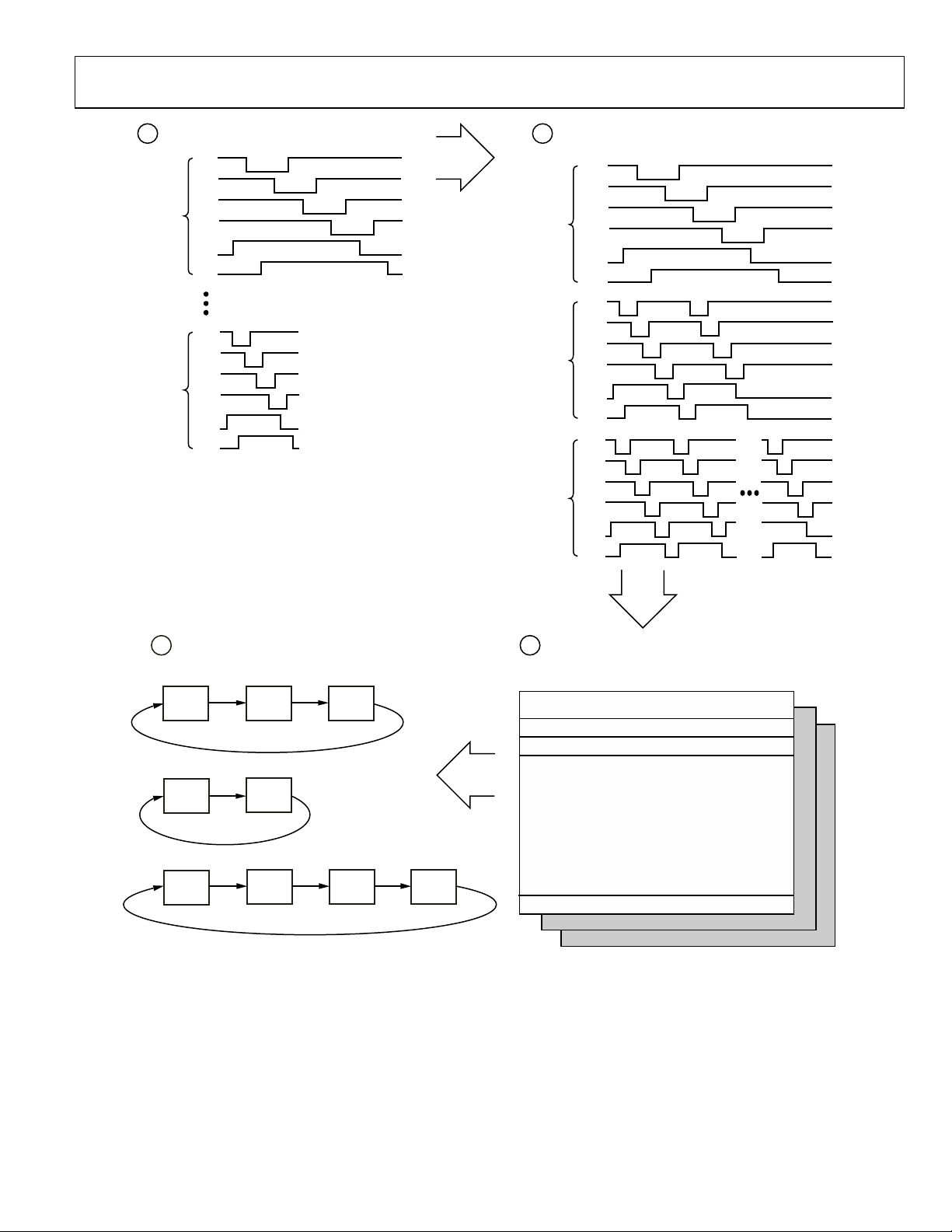
GENERAL DESCRIPTION
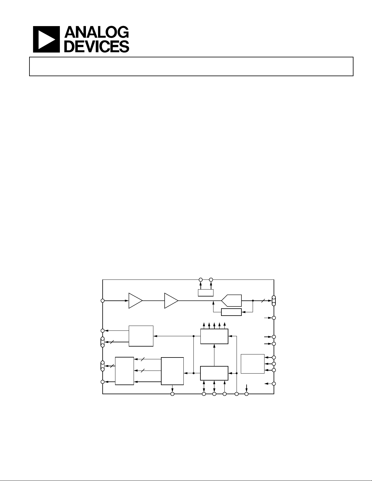
The AD9925 is a complete 36 MHz front end solution for digital still camera and other CCD imaging applications. Based on
the AD9995 product, the AD9925 includes the analog front end
and a fully programmable timing generator (AFETG), combined
with a 10-channel vertical driver (V-driver). A Precision Timing
core allows adjustment of high speed clocks with approximately
600 ps resolution at 36 MHz operation.
The on-chip V-driver supports up to 10 channels for use with
3-field (6-phase) CCDs. Two additional vertical outputs can be
used with CCDs that contain advanced video readout modes.
Voltage levels of up to +15 V and −8 V are supported.
The analog front end includes black level clamping, CDS, VGA,
and a 12-bit ADC. The timing generator and V-driver provide
all the necessary CCD clocks: RG, H-clocks, vertical clocks,
sensor gate pulses, substrate clock, and substrate bias control.
The internal registers are programmed using a 3-wire serial
interface.
Packaged in an 8 mm × 8 mm CSPBGA, the AD9925 is specified over an operating temperature range of −25°C to +85°C.
FUNCTIONAL BLOCK DIAGRAM
6dB TO 42dB
VGA
VERTICAL
TIMING
CONTROL
VSUB
0dB, –2dB, –4dB
V-DRIVER
CDS
HORIZONTAL
DRIVERS
XV1 TO XV8
8
XSG1 TO XSG6
6
SUBCK
CCDIN
RG
H1 TO H4
V1, V2
V3A, V3B
V4, V6
V5A, V5B
V7, V8
SUBCK
Rev. A
Information furnished by Analog Devices is believed to be accurate and reliable.
However, no responsibility is assumed by Analog Devices for its use, nor for any
infringements of patents or other rights of third parties that may result from its use.
Specifications subject to change without notice. No license is granted by implication
or otherwise under any patent or patent rights of Analog Devices. Trademarks and
registered trademarks are the property of their respective owners.
4
10
REFT REFB
Figure 1.
AD9925
VREF
12-BIT
ADC
CLAMP
INTERNAL CLOCKS
PRECISION
TIMING
GENERATOR
SYNC
GENERATOR
HD VD SYNC
One Technology Way, P.O. Box 9106, Norwood, MA 02062-9106, U.S.A.
Tel: 781.329.4700
Fax: 781.326.8703 © 2004 Analog Devices, Inc. All rights reserved.
CLI
www.analog.com
INTERNAL
REGISTERS
CLO
12
DOUT
DCLK
MSHUT
STROBE
SL
SDI
SCK
RSTB
04637-0-001
Page 2

AD9925
TABLE OF CONTENTS
Specifications..................................................................................... 3
Vertical Timing Generation ...................................................... 22
Digital Specifications........................................................................ 4
Vertical Driver Specifications ......................................................... 5
Analog Specifications....................................................................... 6
Timing Specifications....................................................................... 7
Absolute Maximum Ratings............................................................ 8
Package Thermal Characteristics ............................................... 8
ESD Caution.................................................................................. 8
Pin Configuration and Function Descriptions............................. 9
Te r mi n ol o g y .................................................................................... 11
Equivalent Circuits......................................................................... 12
Typical Performance Characteristics ...........................................13
System Overview ........................................................................ 14
Precision Timing High Speed Timing Generation.................. 15
Horizontal Clamping and Blanking......................................... 18
Horizontal Timing Sequence Example.................................... 21
Ver t ic al Tim in g Ex am p l e........................................................... 34
Shutter Timing Control............................................................. 36
Example of Exposure and Readout of Interlaced Frame........... 41
FG_TRIG Operation.................................................................. 43
Analog Front End Description and Operation ...................... 45
Vertical Driver Signal Configuration ...................................... 47
Power-Up and Synchronization ............................................... 51
Standby Mode Operation.......................................................... 55
Circuit Layout Information....................................................... 57
Serial Interface Timing.............................................................. 59
Complete Listing for Register Bank 1 .......................................... 62
Complete Listing for Register Bank 2 .......................................... 66
Complete Listing for Register Bank 3 .......................................... 87
Outline Dimensions ....................................................................... 94
Ordering Guide .......................................................................... 94
REVISION HISTORY
10/04—Data Sheet Changed from Rev. 0 to Rev. A
Changes to Specifications........................................................................................3
Added Stress Disclaimer..........................................................................................8
Changes to Figure 12................................................................................................13
Changes to Figure 22................................................................................................18
Changes to Figure 55................................................................................................45
Change to DC Restore Section ...............................................................................45
Change to Correlated Double Sampler Section....................................................45
Change to ADC Section...........................................................................................46
Change to Digital Data Outputs Section...............................................................46
Added Paragraph to Digital Data Outputs Section..............................................46
Changes to Table 34..................................................................................................55
Change to Circuit Layout Information Section....................................................57
Changes to Register Address Bank 1, Bank 2, and Bank 3 Section ...................60
Changes to Table 40..................................................................................................63
Change to Table 46 ...................................................................................................65
Changes to Tables 47–56, 58–73.............................................................................66
4/04—Revision 0: Initial Version
Rev. A | Page 2 of 96
Page 3
AD9925
SPECIFICATIONS
Table 1.
Parameter Min Typ Max Unit
TEMPERATURE RANGE
Operating –25 +85 °C
Storage –65 +150 °C
POWER SUPPLY VOLTAGES
AVDD (AFE Analog Supply) 2.7 3.0 3.6 V
TCVDD (Timing Core Analog Supply) 2.7 3.0 3.6 V
RGVDD (RG Driver) 2.7 3.0 3.6 V
HVDD (H1 to H4 Drivers) 2.7 3.0 3.6 V
DRVDD (Data Output Drivers) 2.7 3.0 3.6 V
DVDD (Digital) 2.7 3.0 3.6 V
V-DRIVER SUPPLY VOLTAGES
VDVDD (V-Driver Input Logic Supply) 2.7 3.0 3.6 V
VH1, VH2 (V-Driver High Supply for 3-Level Outputs) 10.5 15.0 16.0 V
VM1, VM2 (V-Driver Mid Supply for 3-Level and 2-Level Outputs) –1.0 0.0 +3.0 V
VL1, VL2 (V-Driver Low Supply for 3-Level and 2-Level Outputs) –10.0 –7.5 –6.0 V
POWER DISSIPATION—AFETG Section Only (see Figure 9 for Power Curves)
36 MHz, 3.0 V Supply, 100 pF Load on Each H1 to H4 Output, 20 pF RG Load 370 mW
Standby 1 Mode 10 mW
Standby 2 Mode 10 mW
Standby 3 Mode 1 mW
Power from HVDD Only1 130 mW
Power from RGVDD Only 10 mW
Power from AVDD Only 105 mW
Power from TCVDD Only 42 mW
Power from DVDD Only 57 mW
Power from DRVDD Only 26 mW
POWER DISSIPATION—V-Driver Section Only (VDVDD, VH, VL)
Normal Operation (VH = 15.0 V, VL = −7.5 V)
Standby 1 Mode2 70 mW
Standby 2 Mode2 70 mW
Standby 3 Mode2 110 mW
MAXIMUM CLOCK RATE (CLI) 36 MHz
1
The total power dissipated by the HVDD supply may be approximated using the equation Total HVDD Power = [C
Reducing the H-loading and/or using a lower HVDD supply will reduce the power dissipation. C
2
The power dissipated by the V-driver circuitry depends on the logic states of the inputs as well as actual CCD operation; default dc values are used for each measure-
ment, in each mode of operation. Load conditions are described in the section.
2
Vertical Driver Specifications
60 mW
× HVDD × Pixel Frequency] × HVDD.
is the total capacitance seen by all H-outputs.
LOAD
LOAD
Rev. A | Page 3 of 96
Page 4
AD9925
DIGITAL SPECIFICATIONS
RGVDD = HVDD = DVDD = DRVDD = 2.7 V to 3.6 V, CL = 20 pF, T
Table 2.
Parameter Symbol Min Typ Max Unit
LOGIC INPUTS
High Level Input Voltage VIH 2.1 V
Low Level Input Voltage V
High Level Input Current I
Low Level Input Current I
Input Capacitance C
LOGIC OUTPUTS (Powered by DVDD, DRVDD)
High Level Output Voltage at IOH = 2 mA V
Low Level Output Voltage at IOL = 2 mA VOL 0.5 V
RG and H-DRIVER OUTPUTS (Powered by HVDD, RGVDD)
High Level Output Voltage at Maximum Current VDD – 0.5 V
Low Level Output Voltage at Maximum Current 0.5 V
Maximum Output Current (Programmable) 30 mA
Maximum Load Capacitance (for Each Output) 100 pF
MIN
to T
IL
IH
IL
IN
OH
, unless otherwise noted.
MAX
0.6 V
10 µA
10 µA
10 pF
VDD – 0.5 V
Rev. A | Page 4 of 96
Page 5
AD9925
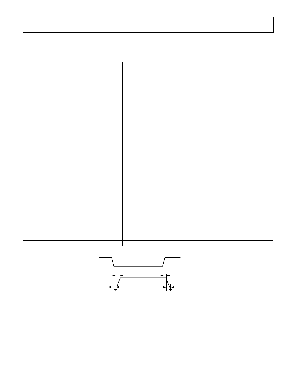
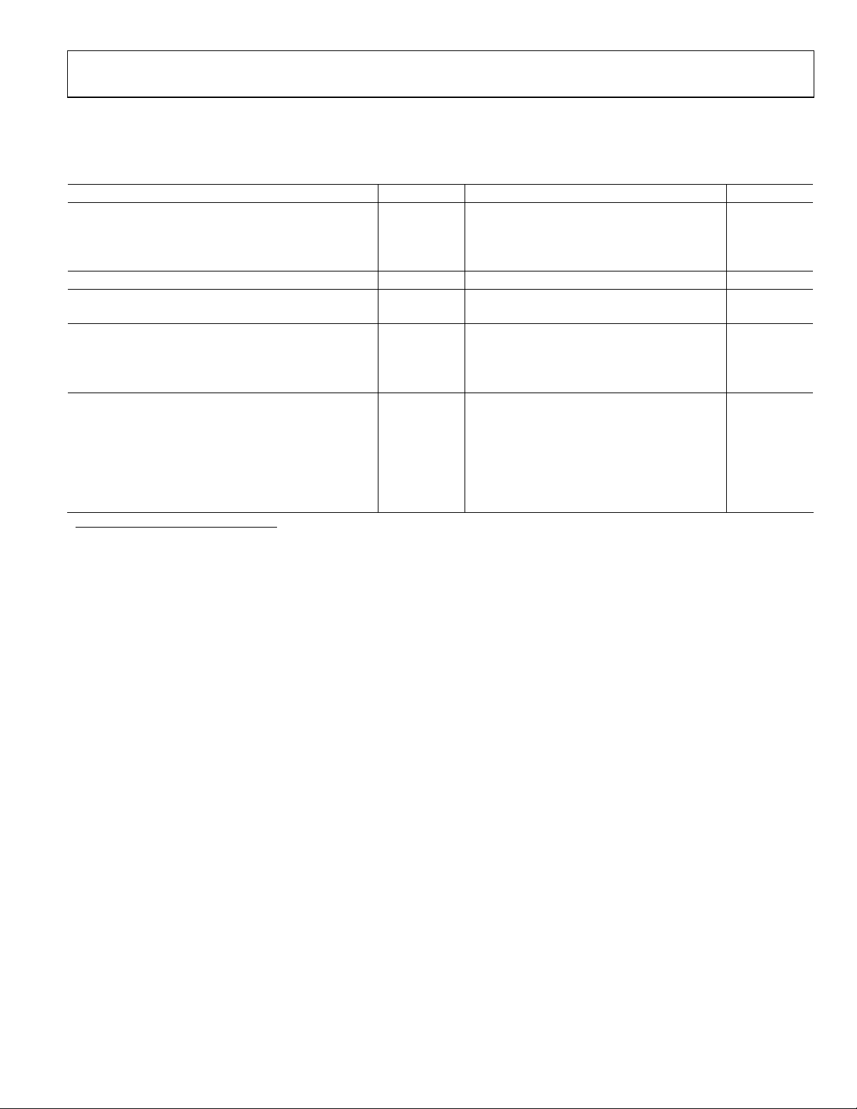
VERTICAL DRIVER SPECIFICATIONS
VDVDD = 3.3 V, VH = 15 V, VM = 0 V, VL = −7.5 V, CL shown in load model, 25°C.
Table 3.
Parameter Symbol Min Typ Max Unit
3-LEVEL OUTPUTS (V1, V2, V3A, V3B, V5A, V5B)
(Simplified Load Conditions, 6000 pF to Ground)
Delay Time, VL to VM and VM to VH t
Delay Time, VM to VL and VH to VM t
Rise Time, VL to VM and VM to VH t
Fall Time, VM to VL and VH to VM t
Output Currents
At −7.25 V 10.0 mA
At −0.25 V −5.0 mA
At +0.25 V 5.0 mA
At +14.75 V −7.2 mA
2-LEVEL OUTPUTS (V4, V6, V7, V8)
(Simplified Load Conditions, 6000 pF to Ground)
Delay Time, VL to VM t
Delay Time, VM to VL t
Rise Time, VL to VM t
Fall Time, VM to VL t
Output Currents
At −7.25 V 10.0 mA
At −0.25 V −5.0 mA
SUBCK OUTPUT
(Simplified Load Conditions, 1000 pF to Ground)
Delay Time, VL to VH t
Delay Time, VH to VL t
Rise Time, VL to VH t
Fall Time, VH to VL t
Output Currents
At −7.25 V 5.4 mA
At +14.75 V −4.0 mA
SERIAL VERTICAL CLOCK RESISTANCE 30 Ω
GND VERTICAL CLOCK RESISTANCE 10 Ω
, t
100 ns
PLM
PMH
, t
200 ns
PML
PHM
, t
500 ns
RLM
RMH
, t
500 ns
FML
FHM
100 ns
PLM
PML
500 ns
RLM
500 ns
FML
100 ns
PLH
200 ns
PHL
200 ns
RLH
200 ns
FHL
200 ns
V-DRIVER
INPUT
V-DRIVER
OUTPUT
50%
10%
90%
t
PLM
t
RLM
,
t
PMH
50%
,
t
,
RMH
,
t
RLH
t
PLH
90%
10%
t
,
t
,
PML
t
PHM
PHL
t
,
t
,
FHM
t
FHL
04637-0-079
FML
Figure 2. Definition of V-Driver Timing Specifications
Rev. A | Page 5 of 96
Page 6
AD9925
ANALOG SPECIFICATIONS
AVDD1 = 3.0 V, f
Table 4.
Parameter Min Typ Max Unit Test Conditions/Comments
CDS Input Characteristics Definition.
Allowable CCD Reset Transient 500 mV
Maximum Input Range before Saturation
0 dB CDS Gain (Default Setting) 1.0 V p-p
−2 dB CDS Gain 1.25 V p-p
−4 dB CDS Gain 1.6 V p-p
Maximum CCD Black Pixel Amplitude +200/–100 mV Positive Offset Definition1
VARIABLE GAIN AMPLIFIER (VGA)
Gain Control Resolution 1024 Steps
Gain Monotonicity Guaranteed
Gain Range
Minimum Gain (VGA Code 0) 6 dB
Maximum Gain (VGA Code 1023) 42 dB
BLACK LEVEL CLAMP
Clamp Level Resolution 256 Steps
Clamp Level Measured at ADC Output.
Minimum Clamp Level (Code 0) 0 LSB
Maximum Clamp Level (Code 255) 255 LSB
ANALOG-TO-DIGITAL CONVERTER (ADC)
Resolution 12 Bits
Differential Nonlinearity (DNL) –1.0 ±0.5 +1.0 LSB
No Missing Codes Guaranteed
Full-Scale Input Voltage 2.0 V
VOLTAGE REFERENCE
Reference Top Voltage (REFT) 2.0 V
Reference Bottom Voltage (REFB) 1.0 V
SYSTEM PERFORMANCE Includes Entire Signal Chain.
Gain Accuracy
Low Gain (VGA Code 0) 5.0 5.5 6.0 dB Gain = (0.0351 × Code) + 5.5 dB.
Maximum Gain (VGA Code 1023) 40.5 41.5 42.5 dB
Peak Nonlinearity, 500 mV Input Signal 0.1 % 12 dB Gain Applied.
Total Output Noise 0.8 LSB rms
Power Supply Rejection (PSR) 50 dB
1
Input signal characteristics are defined as
= 36 MHz, typical timing specifications, T
CLI
MIN
to T
, unless otherwise noted.
MAX
1
AC Grounded Input, 6 dB Gain Applied.
Measured with Step Change on
Supply.
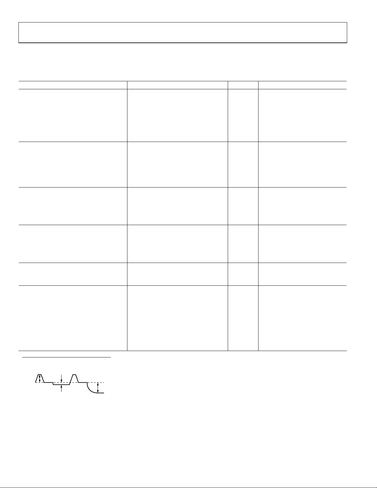
500mV TYP
RESET TRANSIENT
+200mV MAX
OPTICAL BLACK PIXEL
1V MAX
INPUT SIGNAL RANGE
(0dB CDS GAIN)
04637-0-002
Rev. A | Page 6 of 96
Page 7
AD9925
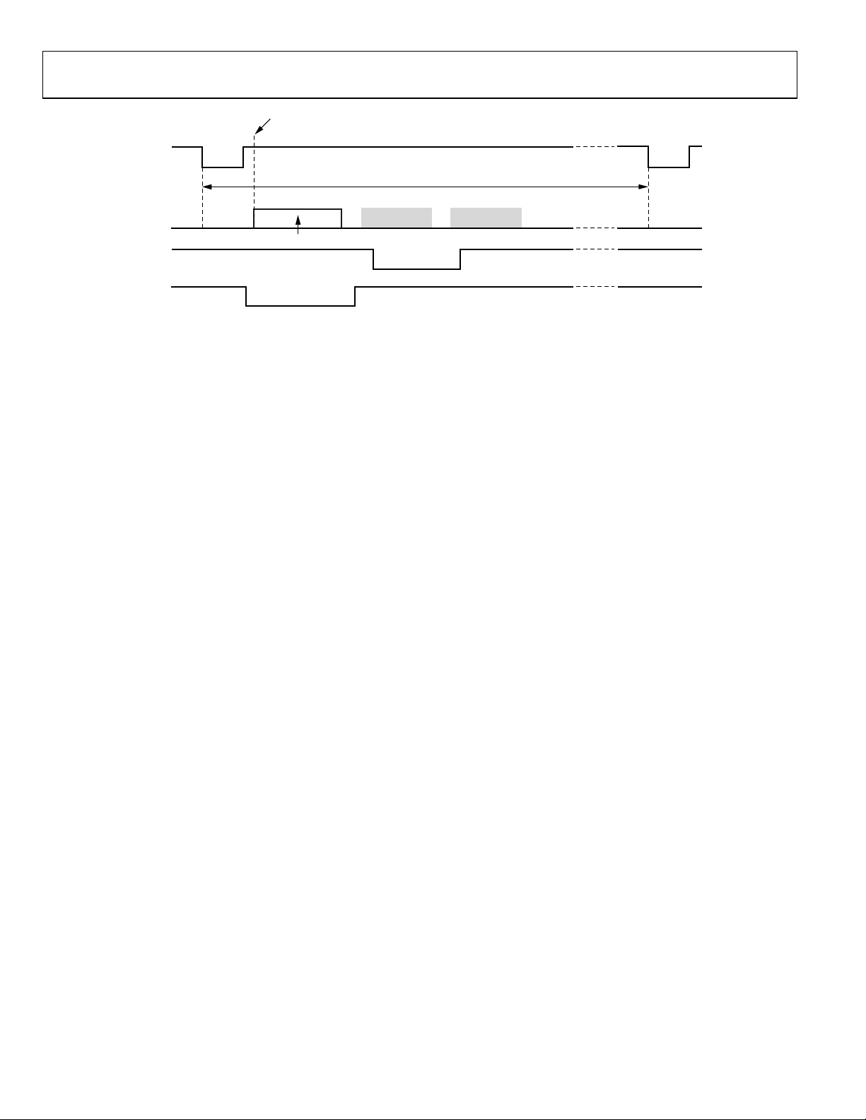
TIMING SPECIFICATIONS
CL = 20 pF, AVDD = DVDD = DRVDD = 3.0 V, f
Table 5.
Parameter Symbol Min Typ Max Unit
MASTER CLOCK, CLI (Figure 17)
CLI Clock Period t
CLI High/Low Pulse Width 11.2 13.9 16.6 ns
Delay from CLI Rising Edge to Internal Pixel Position 0 t
AFE CLPOB PULSE WIDTH
1, 2
(Figure 23 and Figure 29) 2 20 Pixels
AFE SAMPLE LOCATION1 (Figure 20)
SHP Sample Edge to SHD Sample Edge t
DATA OUTPUTS (Figure 21 and Figure 22)
Output Delay from DCLK Rising Edge, Default Value1 t
Inhibited Area for DOUTPHASE Edge Location1 t
Pipeline Delay from SHP/SHD Sampling to DOUT 11 Cycles
SERIAL INTERFACE (Figure 74 and Figure 75)
Maximum SCK Frequency f
SL to SCK Setup Time t
SCK to SL Hold Time t
SDATA Valid to SCK Rising Edge Setup t
SCK Falling Edge to SDATA Valid Hold t
SCK Falling Edge to SDATA Valid Read t
1
Parameter is register-programmable.
2
Minimum CLPOB pulse width is for functional operation only. Wider typical pulses are recommended to achieve good clamp performance.
= 36 MHz, unless otherwise noted.
CLI
CONV
CLIDLY
S1
OD
DOUTINH
SCLK
LS
LH
DS
DH
DV
27.8 ns
6 ns
12.5 13.9 ns
8 ns
SHDLOC SHDLOC + 11
36 MHz
10 ns
10 ns
10 ns
10 ns
10 ns
Rev. A | Page 7 of 96
Page 8
AD9925
ABSOLUTE MAXIMUM RATINGS
Table 6.
Parameter With
Respect To
VDVDD VDVSS
VL VDVSS
VH1, VH2 VDVSS
VM1, VM2 VDVSS
AVDD AVSS –0.3 +3.9 V
TCVDD TCVSS –0.3 +3.9 V
HVDD HVSS –0.3 +3.9 V
RGVDD RGVSS –0.3 +3.9 V
DVDD DVSS –0.3 +3.9 V
DRVDD DRVSS –0.3 +3.9 V
RG Output RGVSS –0.3
H1 to H4 Output HVSS –0.3
Digital Outputs DVSS –0.3
Digital Inputs DVSS –0.3
SCK, SL, SDATA DVSS –0.3
REFT/REFB, CCDIN AVSS –0.3
Junction Temperature
Lead Temperature,
10 s
150 °C
350 °C
Min Max Unit
VDVSS
– 0.3
VDVSS
– 10
VL –
0.3
VL –
0.3
VDVSS
+ 4
VDVSS
+ 0.3
VL +
27
VL +
27
RGVD
D + 0.3
HVDD
+ 0.3
DVDD
+ 0.3
DVDD
+ 0.3
DVDD
+ 0.3
AVDD
+ 0.3
V
V
V
V
V
V
V
V
V
V
Stresses above those listed under Absolute Maximum Ratings
may cause permanent damage to the device. This is a stress
rating only, and functional operation of the device at these or
any other conditions above those indicated in the operational
section of this specification is not implied. Exposure to absolute
maximum rating conditions for extended periods may affect
device reliability.
PACKAGE THERMAL CHARACTERISTICS
Thermal Resistance
CSPBGA Package: θJA = 40.3°C/W
ESD CAUTION
ESD (electrostatic discharge) sensitive device. Electrostatic charges as high as 4000 V readily accumulate
on the human body and test equipment and can discharge without detection. Although this product features
proprietary ESD protection circuitry, permanent damage may occur on devices subjected to high energy electrostatic discharges. Therefore, proper ESD precautions are recommended to avoid performance degradation
or loss of functionality.
Rev. A | Page 8 of 96
Page 9
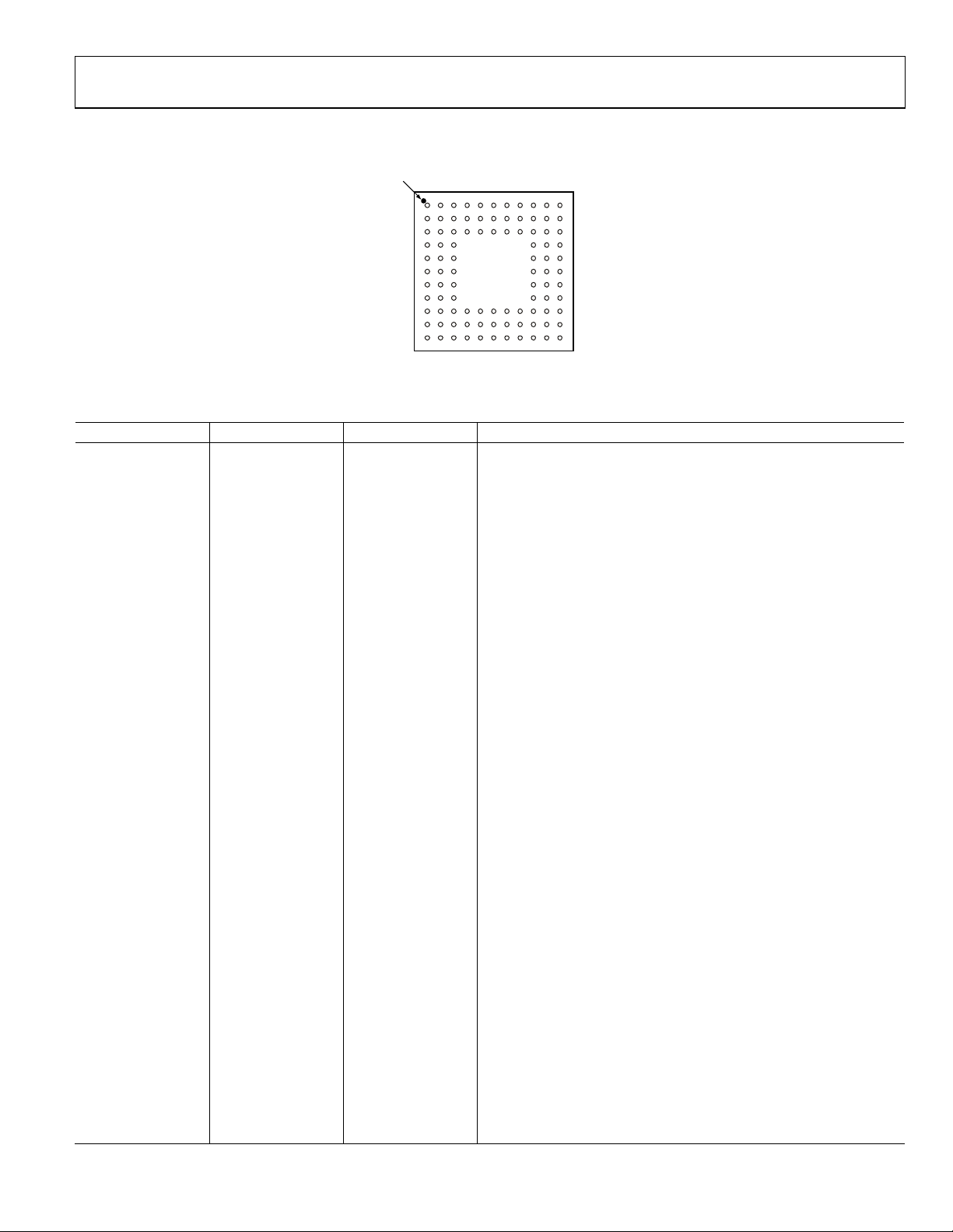
AD9925
PIN CONFIGURATION AND FUNCTION DESCRIPTIONS
A1 CORNER
INDEX AREA
Figure 3. 96-Lead CSPBGA
le 7. Pin Function criptions
Tab Des
nic
Pin No. Mnemo Type Description2
E1, F2, F3 und HVSS P H1 to H4, HL Driver Gro
G2, G3 HVSS P H1 to H4, HL Driver Ground
F1 H1 DO CCD Horizontal Clock 1
G1 H2 DO CCD Horizontal Clock 2
H1, H2, H3 HVDD P H1 to H4, HL Driver Supply
J2, J3 HVDD P H1 to H4, HL Driver Supply
J1 H3 DO CCD Horizontal Clock 3
K1 H4 DO CCD Horizontal Clock 4
K2, L2 RGVSS P RG Driver Ground
L3 RG DO CCD Reset Gate Clock
L4 RGVDD P RG Driver Supply
K3, K4 TCVDD P Analog Supply for Timing Core
J4 CLO DO Clock Output for Crystal
J5 SYNC DI External System Sync Input
K5, L5 TCVSS P Analog Ground for Timing Core
J6 CLI DI Reference Clock Input
K6, L7 AVSS P Analog Ground for AFE
L6 CCDIN AI CCD Signal Input
K7 AVDD P Analog Supply for AFE
L8 REFT AO Voltage Reference Top Bypass
L9 REFB pass AO Voltage Reference Bottom By
J7 MSHUT DO Mechanical Shutter Pulse
J8 SUBCK DO CCD Substrate Clock (E Shutter)
K8 VL P V-Driver Low Supply
K9 VH2 P V-Driver High Supply 2
L10 RSTB DI Reset Bar, Active Low Pulse
K11 SL DI 3-Wire Serial Load Pulse
J11 SCK DI 3-Wire Serial Clock
J10 SDI DI 3-Wire Serial Data Input
J9 V8 VO2 sfer Clock CCD Vertical Tran
K10 V7 VO2 CCD Vertical Transfer Clock
H9 STROBE DO Strobe Pulse
H11 VM2 P V-Driver Mid Supply 2
H10 V6 VO2 CCD Vertical Transfer Clock
G10 V4 VO2 CCD Vertical Transfer Clock
G11 V2 VO2 CCD Vertical Transfer Clock
G9 VD DIO Vertical Sync Pulse (Input in Slave Mode, Output in Master Mode)
1234567 9108
1
11
AD9925
TO
PVIEW
(Not to Scale)
Package Pin Configuration
A
B
C
D
E
F
G
H
J
K
L
04637-0-003
Rev. A | Page 9 of 96
Page 10
AD9925
Pin No. Mnemonic Type1 Description2
F9 HD DIO Horizontal Sync Pulse (Input in Slave Mode, Output in Master Mode)
F10 DVSS P Digital Ground
F11 DVDD ower Supply P Digital Logic P
E9 V5B VO3 CCD Vertical Transfer Clock
D9 V5A VO3 CCD Vertical Transfer Clock
E10 DCLK DO Data Clock Output
D11 D0 DO Data Output (LSB)
C10 D1 DO Data Output
C11 D2 DO Data Output
B10 D3 DO Data Output
B11 D4 DO Data Output
A10 D5 DO Data Output
A9 D6 DO Data Output
C9 V3B VO3 ck CCD Vertical Transfer Clo
B9 V3A 3 lock VO CCD Vertical Transfer C
B8 V1 VO3 CCD Vertical Transfer Clock
A8 D7 DO Data Output
B7 D8 DO Data Output
A7 D9 DO Data Output
B6 D10 DO Data Output
A6 D11 DO Data Output (MSB)
C8 VM1 P V-Driver Mid Supply 1
C7 VH1 P V-Driver High Supply 1
C6 VL P V-Driver Low Supply
C5 DRVDD P Data Output Driver Supply
B5 DRVSS P Data Output Driver Ground
A5 VSUB DO CCD Substrate Bias
A4 VDVDD P V-Driver Logic Supply
B4 VDVSS P V-Driver Logic Ground
A1, A2, A3 NC Not Internally Connected
B1, B2, B3 NC Not Internally Connected
C1, C NC Not Internally Connected 2, C3
C4, D1, D2 NC Not Internally Connected
D3, E2, E3 NC Not Internally Connected
D10, E11 NC Not Internally Connected
L1, L11, A11 NC Not Internally Connected
1
AI = Analog Input; AO = Analog Output; DI = Digital Input; DO = Digital Output; DIO = Digital Input/Output; P = Power; VO2 = V-Driver Output 2-Level; VO3 = V-Driver
Output 3-Level.
2
See Figure 73 for circuit configuration.
Rev. A | Page 10 of 96
Page 11

AD9925
TERMINOLOGY
Differential Nonlinearity (DNL)
An ideal ADC exhibits code transitions that are exactly 1 LSB
apart. DNL is the deviation from this ideal value. Thus, every
code must have a finite width. No missing codes guaranteed to
12-bit resolution indicates that all 4096 codes, respectively, must
be present over all operating conditions.
Peak Nonlinearity
Peak nonlinearity, a full signal chain specification, refers to the
peak deviation of the output of the AD9925 from a true straight
line. The point used as zero scale occurs 0.5 LSB before the first
code transition. Positive full scale is defined as a Level 1 and is
0.5 LSB beyond the last code transition. The deviation is measured from the middle of each particular output code to the true
straight line. The error is then expressed as a percentage of the
2 V ADC full-scale signal. The input signal is always appropriately gained up to fill the ADC’s full-scale range.
Total Output Noise
The rms output noise is measured using histogram techniques.
The standard deviation of the ADC output codes is calculated
in LSB and represents the rms noise level of the total signal
chain at the specified gain setting. The output noise can be converted to an equivalent voltage, using the relationship 1 LSB =
ADC Full Scale/2
ADC. For the AD9925, 1 LSB is 0.488 mV.
Power Supply Rejection (PSR)
The PSR is measured with a step change applied to the supply
pins. The PSR specification is calculated from the change in the
data outputs for a given step change in the supply voltage.
n
codes, where n is the bit resolution of the
Rev. A | Page 11 of 96
Page 12
AD9925
EQUIVALENT CIRCUITS
AVDD
DVDD
DATA
THREE-
STATE
R
AVSS AVSS
Figure 4. CCDIN
DVDD
04637-0-004
DRVDD
100kΩ
300Ω
DVSS
04637-0-075
Figure 7. SL and RSTB Inputs
HVDD OR
RGVDD
RG, H1 TO H4
DOUT
THREE-STATE
OUTPUT
DVSS DRVSS
Figure 5. Digital Data Outputs
DVDD
330Ω
DVSS
04637-0-006
04637-0-005
HVSS OR
RGVSS
Figure 8. H1 to H4, RG Drivers
04637-0-007
Figure 6. Digital Inputs
Rev. A | Page 12 of 96
Page 13
AD9925
TYPICAL PERFORMANCE CHARACTERISTICS
450
400
350
300
250
POWER DISSIPATION (mW)
200
VDD = 3.3V
V
DD
= 3.0V
V
DD
= 2.7V
40
35
30
25
20
15
NOISE (LSB)
10
5
150
SAMPLE RATE (MHz)
Figure 9. Power vs. Sample Rate
1.0
0.8
0.6
0.4
0.2
0
LSB
–0.2
–0.4
–0.6
–0.8
–1.0
0 500 200015001000 2500 35003000 4000
ADC OUTPUT CODE
Figure 10. Typical DNL Performance
45
40
35
30
25
20
GAIN (dB)
15
10
5
0
0 100 500400200 300 600 900800700 1000
GAIN CODE (Decimal)
Figure 11. Typical VGA Gain Curve
0
3618 24 30
04637-0-084
04637-0-080
0 100 500400200 300 600 900800700 1000
GAIN CODE (Decimal)
Figure 12. Total Output Noise vs. VGA Gain
5
4
3
2
1
0
LSB
–1
–2
–3
–4
–5
0 500 200015001000 2500 35003000 4000
ADC OUTPUT CODE
Figure 13. Typical INL Performance
04637-0-083
04637-0-082
04637-0-081
Rev. A | Page 13 of 96
Page 14
AD9925
SYSTEM OVERVIEW
Figure 14 shows the typical system block diagram for the
AD9925 used in master mode. The CCD output is processed
the AD9925’s AFE circuitr
y, which consists of a CDS, VGA,
black level clamp, and ADC. The digitized pixel informa
sent to the digital image processor chip, which performs the
postprocessing and compression. To operate the CCD, all CCD
timing parameters are programmed into the AD9925 from the
system microprocessor through the 3-wire serial interface.
From the system master clock, CLI, provided by the image
processor or external crystal, the AD9925 generates the CCD’s
horizontal and vertical clocks and internal AFE clocks. E
synchronization is provided by a SYNC pulse from the micro
processor, which will reset internal counters and resync the VD
and HD outputs. The AD9925 also contains an optional reset
pin, RSTB, which may be used to perform an asynchronous
hardware reset function.
V1A, V2, V3A, V3B, V4, V5A,
V5B, V6, V7, V8, SUBCK, VSUB
H1 TO H4, RG
SERIAL
INTERFACE
DOUT
DCLK
HD, VD
CLI
DIGITAL
IMAGE
PROCESSING
ASIC
µP
CCD
CCDIN
MSHUT
STROBE
AD9925
AFETG
+
V-DRIVER
SYNC
RSTB
Figure 14. Typical System Block Diagram, Master Mode
by
tion is
xternal
-
04637-0-008
Alternatively, the AD9925 may be operated in slave mode, in
which the VD and HD are provided externally from the image
processor. In this mode, all AD9925 timing will be synchronized with VD and HD.
The H-drivers for H1 to H4 and RG are included in the
AD9925, allowing these clocks t directly connected to the
CCD. An H-d d. A high
rive voltage of up to 3.3 V is supporte
o be
voltage V-driver is also included for the vertical clocks, allowing
irect connection to the CCD. The SUBCK and VSUB signals
d
ay require external transistors, depending on the CCD used.
m
The AD9925 also includes programmable MSHUT and
STROBE outputs, which may be used to trigger mechanical
shutter and strobe (flash) circuitry.
Figure 15 and Figure 16 show the maximum horizontal and
vertical counter dimensions for the AD9925. All internal horizontal and vertical clocking is controlled by these counters to
specify line and pixel locations. Maximum HD length is 8192
pixels per line, and maximum VD length is 4096 lines per field.
MAXIMUM
COUNTER
DIMENSIONS
13-BIT HORIZONTAL = 8192 PIXELS MAX
12-BIT VERTICAL = 4096 LINES MAX
04637-0-009
Figure 15. Vertical and Horizontal Counters
MAX VD LENGTH IS 4096 LINES
VD
HD
CLI
MAX HD LENGTH IS 8192 PIXELS
04637-0-010
Figure 16. Maximum VD/HD Dimensions
Rev. A | Page 14 of 96
Page 15
AD9925
PRECISION TIMING HIGH SPEED TIMING GENERATION
The AD9925 generates high speed timing signals using the flexible Precision Timing core. This core is the foundation that gen-
erates the timing used for both the CCD and the AFE: the reset
gate (RG), horizontal drivers H1 to H4, and the SHP/SHD sample
clocks. The unique architecture provides precise control over
the horizontal CCD readout and the AFE correlated double sampling, allowing the system designer to optimize image quality.
The high speed timing of the AD9925 operates the same in
either master or slave mode configuration. For more information on synchronization and pipeline delays, see the Power-Up
and Synchronization section.
Timing Resolution
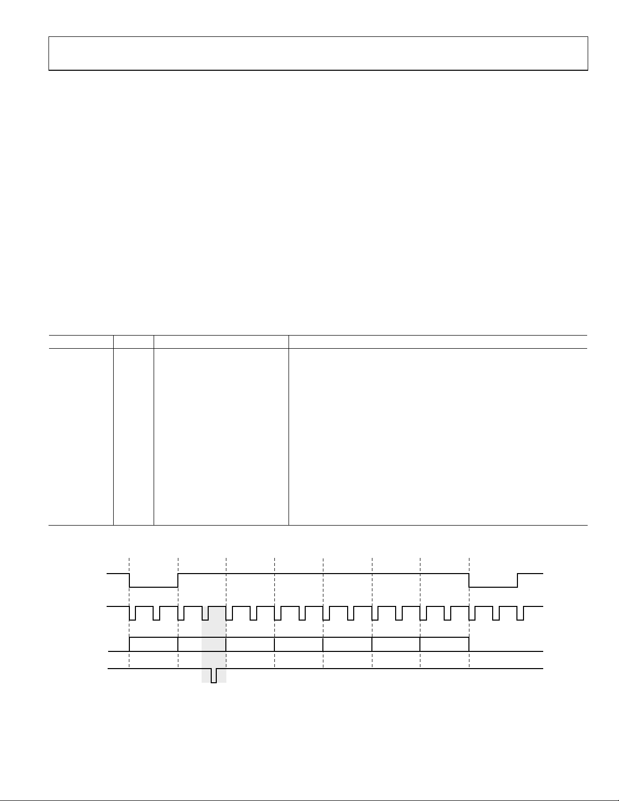
The Precision Timing core uses a 13 master clock input (CLI) as
a reference. This clock should be the same as the CCD pixel
clock frequency. Figure 17 illustrates how the internal timing
core divides the master clock period into 48 steps or edge positions. Using a 20 MHz CLI frequency, the edge resolution of the
Precision Timing core is 1 ns. If a 1× system clock is not available, it is also possible to use a 2× reference clock by programming the CLIDIVIDE register (Addr x30). The AD9925 will
then internally divide the CLI frequency by two.
crystal can be placed between the CLI and CLO pins to generate
the master clock for the AD9925. For more information on
using a crystal, see Figure 72.
High Speed Clock Programmability
Figure 18 shows how the high speed clocks RG, H1 to H4, SHP,
and SHD are generated. The RG pulse has programmable rising
and falling edges and may be inverted using the polarity control.
The horizontal clocks, H1 and H3, have programmable rising
and falling edges and polarity control. The H2 and H4 clocks
are always inverses of H1 and H3, respectively. Table 8 summarizes the high speed timing registers and their parameters.
Figure 19 shows the typical 2-phase H-clock arrangement in
which H3 and H4 are programmed for the same edge location
as H1 and H2.
The edge location registers are 6 bits wide, but there are only
48 valid edge locations available. Therefore, the register values
are mapped into four quadrants, with each quadrant containing
12 edge locations. Table 9 shows the correct register values for
the corresponding edge locations.
The AD9925 also includes a master clock output, CLO, which is
the inverse of CLI. This output can be used as a crystal driver. A
POSITION
CLI
1 PIXEL
PERIOD
t
CLIDLY
NOTES
1. PIXEL CLOCK PERIOD IS DIVIDED INTO 48 POSITIONS, PROVIDING FINE EDGE RESOLUTION FOR HIGH SPEED CLOCKS.
2. THERE IS A FIXED DELAY FROM THE CLI INPUT TO THE INTERNAL PIXEL PERIOD POSITION (
P[0] P[48] = P[0]P[12] P[24] P[36]
Figure 17. High Speed Clock Resolution from CLI Master Clock Input
t
CLIDLY
= 6ns TYP).
04637-0-011
Rev. A | Page 15 of 96
Page 16
AD9925
CCD
SIGNAL
1
RG
56
H1
H2
78
H3
H4
PROGRAMMABLE CLOCK POSITIONS:
1. RG RISING EDGE.
2. RG FALLING EDGE.
3. SHP SAMPLE LOCATION.
4. SHD SAMPLE LOCATION.
5. H1 RISING EDGE POSITION AND 6: H1 FALLING EDGE POSITION (H2 IS INVERSE OF H1).
7. H3 RISING EDGE POSITION AND 8: H3 FALLING EDGE POSITION (H4 I
2
3
4
S INVERSE OF H3).
Figure 18. High Speed Clock Programmable Locations
04637-0-012
Figure 20 sho fault timi ns for all
speed clo
H-Driver and puts
In addition to the pum tions, the AD9925
features on-chip o
puts. These driv
CD inputs. The H-driver and RG current can be adjusted for
C
ptimum rise/fall time with a particular load by using the
o
RVCONTROL register (Addr x35). The 3-bit drive setting for
D
ws the de ng locatio of the high
ck signals.
RG Out
rogra mable timing posi
tpu vers for the RG
t dri
ers are p erful enough to
ow
and H1 to H4 out-
directly drive the
each output is adjustable in 4.1 mA increments, with the minimum setting of 0 equal to OFF or three-state and the
etting of 7 equal to 30.1 mA.
s
As shown in Figure 18, Figure 19, and Figure
inverses of H1 and H3,outputs are respectively. The H1/H
ossover voltage is approximately e output swing. The
cr 50% of th
ssover voltage is not programm
cro able.
maximum
20, the H2 and H4
2
Digital Da
The AD9925 data output and DCLK phase are programmable
using the DOUTPHASE register (Addr
edge from 0 to 47 may be programmed, a
Normally, the DOUT and DCLK signals will track
based on the DOUTPHASE register contents. The DCLK o
put phase can also be held fixed with respect to the data outputs
by changing the DCLKMODE register high (Addr x37, Bit [6]).
In this mode, the DCLK output will remain at a fixed phase
equal to CLO (the inverse of CLI), while the data output phase
is still programmable.
There is a fixed output delay from the DCLK rising edge to the
DOUT transition, called t
four values between 0 ns and 12 ns by using the DOUTDELAY
register (Addr x37, he default value is 8 ns
The pi AD9925 is shown in
After t by SHD, there is an
delay u
ta Outputs
x37, Bits [5:0]). Any
s shown in Figure 21.
in phase,
ut-
. This delay can be programmed to
OD
Bits [8:7]). T .
peline delay through the Figure 22.
he CCD input is sampled 11 cycle
ntil the data is available.
Table 8. Timing Core Register Parameters for H1, H3, RG, SHP/SHD
arameter Length Range Description
P
Polarity 1 b High/Low Polarity Control for H1, H3, and RG (0 = No Inversion, 1 = Inversion)
Positive Edge 6 b 0 to 47 Edge Location Positive Edge Location for H1, H3, and RG
Negative Edge 6 b 0 to 47 Edge Location Negative Edge Location for H1, H3, and RG
Sampling Location 6 b 0 to 47 Edge Location Sampling Location for Internal SHP and SHD Signals
Drive Strength 3 b 0 to 47 Current Steps Drive Current for H1 to H4 and RG Outputs (4.1 mA per Step)
Rev. A | Page 16 of 96
Page 17
AD9925
CCD
SIGNAL
RG
H1/H3
H2/H4
NOTE
1. USING THE SAME TOGGLE POSITIONS FOR H1 AND H3 GENERATES STANDARD 2-PHASE H-CLOCKING.
04637-0-013
Figure 19. 2-Phase H-Clock Operation
Table 9. Precision Timing Edge Locations
Quadrant Edge Location (Dec) Register Value (Dec) Register Value (Bin)
I 0 to 11 0 to 11 000000 to 001011
II 12 to 23 010000 to 011011 16 to 27
I 24 to 35 32 to 43 100000 to 101011 II
IV 36 to 47 48 to 59 110000 to 111011
POSITION
PIXEL
PERIOD
RG
H1/H3
P[0]
RGr[0] RGf[12]
Hr[0] Hf[24]
P[24]P[12] P[36]
P[48] = P[0]
H2/H4
SHP[24]
CCD
SIGNAL
NOTES
1. ALL SIGNAL EDGES ARE FULLY PROGRAMMABLE TO ANY OF THE 48 POSITIONS WITHIN ONE PIXEL PERIOD.
2. DEFAULT POSITIONS FOR EACH SIGNAL ARE SHOWN.
t
S1
SHD[48]
04637-0-014
Figure 20. High Speed Timing Default Locations
Rev. A | Page 17 of 96
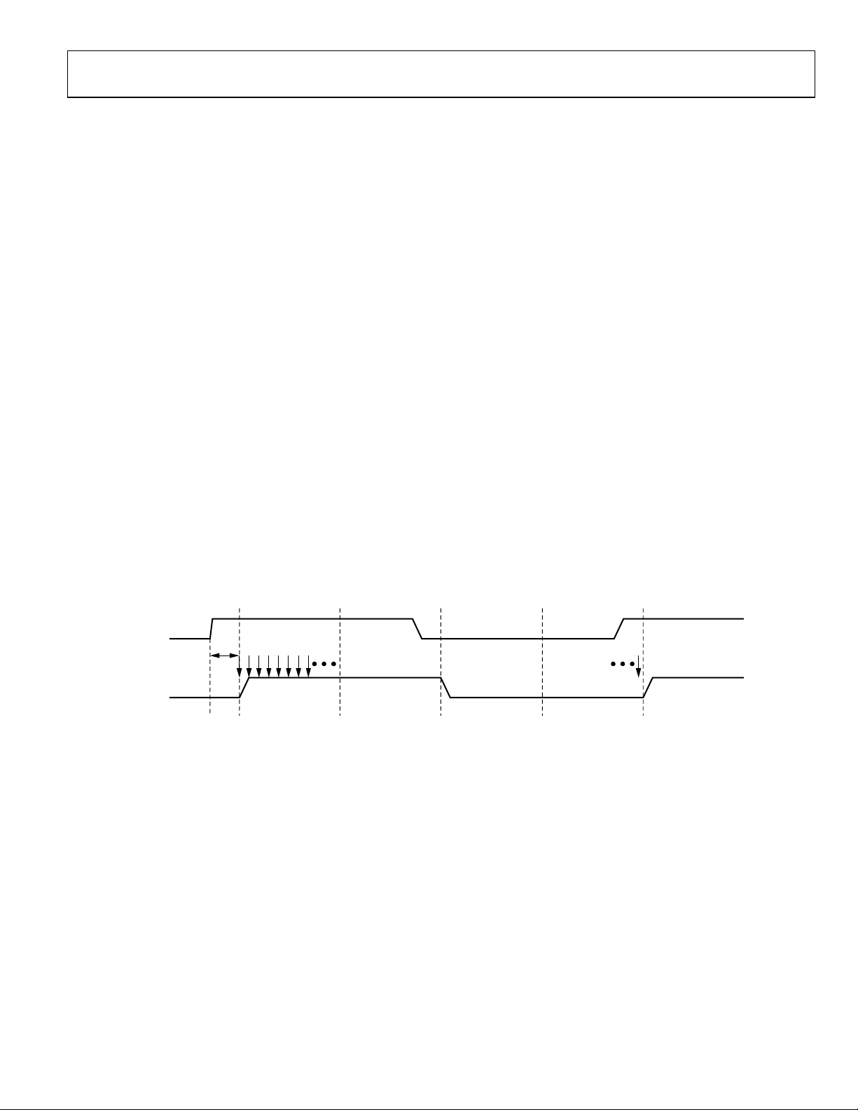
Page 18
AD9925
.
2
.
3
(
CLI
CCDIN
SHD
(INTERNAL)
P[0]
PIXEL
PERIOD
DCLK
t
OD
DOUT
NOTES
1. DATA OUTPUT (DOUT) AND DCLK PHASE IS ADJUSTABLE WITH RESPECT TO THE PIXEL PERIOD
. WITHIN 1 CLOCK PERIOD, THE DATA TRANSITION CAN BE PROGRAMMED TO 48 DIFFERENT LOCATIONS
. OUTPUT DELAY
t
) FROM DCLK RISING EDGE TO DOUT RISING EDGE IS PROGRAMMABLE.
OD
P[12]
P[24]
P[36]
Figure 21. Digi tal Output Phase Adjustment
t
CLIDLY
N– 1
N N + 1
SAMPLE PIXEL N
N + 2
N + 3
N + 4
P[48] = P[0]
04637-0-015
N + 12N + 11N + 10N + 9N + 8N + 7 6 N + 13N +N + 5
ADC DOUT
(INTERNAL)
DCLK
DOUT
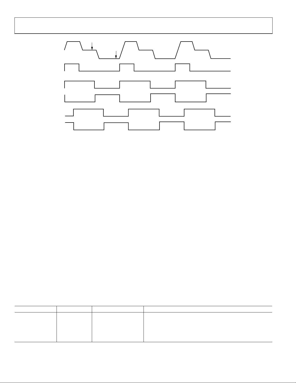
HORIZ CLAM ING AND BLANKING
ONTAL P
The AD9925’s rizon amping and blanking pu are fully
N – 13
N – 12
t
DOUTINH
N – 13
N – 12
NOTES
1. TIMING VALUES SHOWN ARE SHDLOC = 0, WITH DCLKMOD
2. HIGHER VALUES OF SHD AND/OR DOUTPHASE WILL SHI
3. INHIBIT TIME FOR DOUT PHASE IS DEFINED BY t
11 EDGE LOCATIONS FOLLOWING SHDLOC NOT BE USED
4. RECOMMENDED VALUE FOR DOUT PHASE IS TO USE THE
ECOMMENDED VALUE FOR
5. R
6. THE DOUT LATCH CAN BE BYPASSED U
DOUT PINS. THIS CONFIGURATION IS R
t
(DOUT DLY) IS 4ns.
OD
ho tal cl lses
programmable to suit a variety of applications. Individu
trol is provided for CLPOB, PBLK, and HBLK during th
ent regions of each fiel is allows th ping
d. Th e dark pixel clam
and blanking patterns to be changed at each stage of the
out, which accommodates the different image transfer t
N– 8N– 9N – 10N – 11
PIPELINE LATENC
N– 8N– 9N – 10N – 11
, W
DOUTINH
SING REGISTER 0x03, BIT [4] = 1, SO THAT THE ADC DATA OUTPUTS APPEAR DIRECTLY AT THE
ECOMMENDED IF ADJUSTABLE DOUT PHASE IS NOT REQUIRED.
Figure utput Pipeline Delay
22. Digital Data O
al con-
e differ-
read-
iming
and high speed line shifts.
Individual CLPOB and PBLK Patterns
he AFE horizontal timing consists of CLPOB and PBLK, as
T
wn in Figure 23. These two signals are independently pro-
sho
rammed using the registers in Table 10. SPOL is the start po-
g
larity for the signal, and TOG1 and TOG2 are the first and second toggle positions of the pulse. Both signals ar
e active low
and should be programmed accordingly.
N– 6N– 7
Y = 11 CYCLES
NN– 7 N– 3N– 4N– 5– 6 N– 2
E = 0.
FT DOUT TRA
HICH IS EQ
FOR THE DOUTPHASE LOCATION.
SHPLOC EDGE OR THE 11 EDGES FOLLOWING SHPLOC.
NSITION TO THE RIGHT, WITH RESPECT TO CLI LOCATION.
UAL TO SHDLOC PLUS 11 EDGES. IT IS RECOMMENDED THAT THE
N– 3N– 4N– 5 N– 2
N– 1
A separate pattern for CLPOB and PBLK may be programmed
for every 10 vertical sequences. As described in the Vertical
Timing Generation section, up to 10 separa
can be created, each containing a unique pulse pattern for
CLPOB and PBLK. Figure 37 shows how the sequence change
positions divide the readout field into different regions. A different vertical sequence can be assigned to each region, allowing
the CLPOB and PBLK signals to
each change in the vertical timing.
CLPOB Masking Area
Additionally, the AD9925 allows the CLPOB signal to be disabled during certain lines in the field without changing any of
the existing CLPO
B pattern settings. There are two ways to use
CLPOB masking. First, the six CLPOBMASK registers can be used
N + 1NN + 2
N + 1
N– 1
N
N + 2
04637-A-001
te vertical sequences
be changed accordingly with
Rev. A | Page 18 of 96
Page 19
AD9925
to specify six individual lines within th
contain an e CLPOB ulse. CLP ow for this
mode of oper ion.
Second, th
of adjacent
activ p MASKTYPE is set l
at
e CLPMA
lines e CLPMAS ue
SK re cif
gisters can be used to spe
. Th
grammed to specify the starting and ending lines in the f
the CLPOB patterns will be ignored. There are three sets
and end valu allowi to three CLPOB masking eas to be
created. CLP ASKTYP is set high for this mode of o eration.
The CLPOB asking sters are not specific to a ce ain vertical
sequence; the are alw active for any existing field timing.
To disable th CLPO sking feature, these regist should
es, ng up ar
M E p
m regi rt
y ays of
e B ma ers
be set to the maximum value of 0xFFF (default value).
Table 10. CLPOB and PBLK Pattern Registers
Register Length Range Descr
SPOL 1 b High/Low Starting Polarity of CLPOB/PBLK for Vertical Sequence 0 to 9.
TOG1 12 b 0 to 4095 Pixel Location First Toggle Position within Line for Vertical Sequence 0 to 9.
TOG2 12 b 0 to 4095 Pixel Location Second Toggle Position within Line for Vertical Sequence 0 to 9.
CLPOBMASK 12 b 0 to 4095 Line Location
CLPMASKTYPE 1 b High/Low
e field. These lines will not
K start and end line val
Individual HBLK Patterns
The HBLK programmable timing shown in Figure 24 is similar
olarity control. Only
itionally, there is a polarity
2 = H4 = High
he CLPOB
ach vertical
e used with
y blocks
s are pro-
ield, where
of start
to CLPOB and PBLK, but there is no start p
the toggle positions are used to designate the start and the stop
positions of the blanking period. Add
control HBLKMASK that
clock signals H1 to H4 durin
designates the polarity of the horizontal
g the blanking period. Setting
HBLKMASK high will set H1 = H3 = Low and H
during the blanking, as shown in Figure 25. As with t
and PBLK signals, HBLK registers are available in e
sequence, which allow different blanking signals to b
different vertical timing sequences.
One additional feature is the ability to enable th
e H3/H4 signals
to remain active during HBLK. To do this, set register Bit D6 in
Addr 0xE7 equal to 1. This feature is usef
ul if the H3 output is
used to drive the HL (last horizontal gate) input of the CCD.
iption
CLPOBMASK0 thr e
CLPOB pulse to be ed to specify
three ranges of ad
ough CLPOBMASK5 specify six individual lines in the field for th
temporarily disabled. These registers can also be us
jacent lines, rather than six individual lines.
When set low (default), the CLPOBMASK registers select individual lines in the field
to disable the CLPOB pulse. When set high, the range masking is enabled, allowing
up to three blocks of adjacent lines to have the CLPOB signal masked. CLPOBMASK0 and CLPOBMASK1 are the start/end of the first block of lines, CLPOBMASK2
and CLPOBMASK3 are the start/end of the second block, and CLPOBMASK4 and
CLPOBMASK5 are the start/end of the third block.
HD
CLPOB
1
PBLK
NOTES
PROGRAMMABLE SETTINGS:
1. START POLARITY (CLAMP AND BLANK REGION ARE ACTIVE LOW).
2. FIRST TOGGLE POSITION.
3. SECOND TOGGLE POSITION.
ACTIVE
32
ACTIVE
04637-0-017
Figure 23. Clamp and Preblank Pulse Placement
Rev. A | Page 19 of 96
Page 20
AD9925
K
Table 11. HBLK Pattern Registers
Register Length Range Description
HBLKMASK 1 b High/Low Masking Polarity for H1/H3 (0 = H1/H3 Low, 1 = H1/H3 High).
H3HBLKOFF 1 b High/Low Addr 0xE7, Bit [6]. Set = 1 to keep H3/H4 active during HBLK pulse. Normal set to 0.
HBLKALT 2 b 0 to 3 Alternation Mode
HBLKTOG1 12 b 0 to 4095 Pixel Location First Toggle Position within Line for Each Vertical Sequence 0 to 9.
HBLKTOG2 12 b 0 to 4095 Pixel Location Second Toggle Position within Line for Each Vertical Sequence 0 to 9.
HBLKTOG3 12 b 0 to 4095 Pixel Location Third Toggle Position within Line for Each Vertical Sequence 0 to 9.
HBLKTOG4 12 b 0 to 4095 Pixel Location Fourth Toggle Posit ch Vertical Sequence 0 to 9. ion within Line for Ea
HBLKTOG5 12 b 0 to 4095 Pixel Location Fifth Toggle Position within Line for Each Vertical Sequence 0 to 9.
HBLKTOG6 12 b 0 to 4095 Pixel Location Sixth Toggle Position within Line for Each Vertical Sequence 0 to 9.
Enables Odd/Even A
0 = Disable Alternat
G1 to TOG2 O
1 = TO
2 = 3 = TO
G1to TOG
lternation of HBLK Toggle Positions.
ion.
dd, TOG3 to TOG6 Even.
2 Even, TOG3 to TOG6 Odd.
Generating S Bpecial H LK Patterns
There are six oggle ions availab for HBLK. Normally,
only two of the toggle positions are use
dard HBLK interval. However, the addi
may be used to generate special HBLK
Figure 26. The pattern in this example
tions to generate two extra groups of pu
interval. By changing the toggle positio atterns can
t posit le
d to generate the stan-
tional toggle positions
patterns, as shown in
uses all six toggle posi-
lses during the HBLK
ns, different p
be created.
HD
12
HBL
PROGRAMMABLE SETTINGS:
1. FIRST TOGGLE POSITION = START OF BLANKING.
2. SECOND TOGGLE POSITION = END OF BLANKING.
HD
BLANK BLANK
Figure 24. Horizontal Blanking (HBLK) Pulse Placement
Generating HBLK Line Alternation
One further feature of the AD9925 is the ability to alternate different HBLK toggle positions on odd and even lines. This may be
used in conjunction with vertical pattern odd/even alternation or
on its own. When a 1 is writte
n to the HBLKALT register, TOG1
and TOG2 are used on odd lines, while TOG3 to TOG6 are
used on even lines. Writing a 2 to the HBLKALT register give
the opposite result: TOG1 and TOG2 are used on even lines,
while TOG3 to TOG6 are
used on odd lines. See the Vertical
Timing Generation section for more information.
04637-0-018
s
HBLK
H1/H3
H1/H3
H2/H4
NOTE
1. THE POLARITY OF H1 DURING BLANKING IS PROGRAMMABLE (H2 IS OPPOSITE POLARITY OF H1).
Figure 25. HBLK Masking Control
Rev. A | Page 20 of 96
04637-0-019
Page 21
AD9925
HBLK
H1/H3
H2/H4
TOG1 TOG2 TOG3 TOG4 TOG5 TOG6
SPECIAL H-BLANK PATTERN IS CREATED USING MULTIPLE HBLK TOGGLE POSITIONS
Figure 26. Generating Special HBLK Patterns
Increasing H-Clock Width during HBLK
The AD9925 will also allow the H1 to H4 pulse width to be
increased during the HBLK interval. The H-clock pu
lse width
can increase by reducing the H-clock frequency (see Figure 27).
he HBLKWIDTH register, at Bank 1 Address 0x38, is a 3-bit
T
register that allows the H-clock frequency to be reduced by 1/2,
1/4, 1/6, 1/8, 1/10, 1/12, or 1/14. The reduced frequen
only occur for H1 to H4 pulses that are located within t
BLK area.
H
cy will
he
Table 12. HBLK Width Register
Register Length Range Description
HBLKWIDTH 3 b 1 to 1/14
Controls H1 to H4 widt
h
during HBLK as a fraction of pixel rate
0: same frequency as
pixel rate
1: 1/2 pixel frequency,
i.e., doubles the H1 to H4
pulse width
2: 1/4 pixel frequency
3: 1/6 pixel frequency
4: 1/8 pixel frequency
5: 1/10 pixel frequency
6: 1/12 pixel frequency
7: 1/14 pixel frequency
04637-0-020
HORIZONTAL TIMING SEQUENCE EXAMPLE
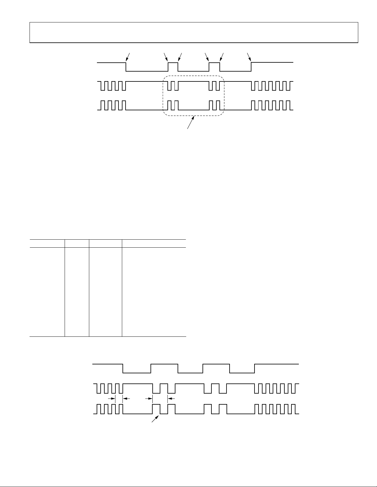
Figure 28 shows an exampl CCD layout. The horizontal register
contains 28 d
ummy pixels, which will occur on each line clocked
from the CCD. In the vertical direction, there are 10 optical black
(OB) lines at the front of the readout and 2 at the back of the
readout. The horizontal direction has 4 OB pixels in the front
and 48 in the
back.
Figure 29 shows the basic sequence layout to be used during the
effective pixel readout. The 48 OB pixels at the end of each
are used for the CLPOB signals. PBLK is optional and is often
used to blank the digital outputs during the noneffective CCD
pixels. HBLK is used during the vertical shift interval. The
HBLK, CLPOB, and PBLK parameters are programmed in the
vertical sequence registers.
More elaborate clamping schemes may be used, such as addin
in a separate sequence to clamp during the entire shield OB
lines. This requires configuring a separate vertical sequence for
reading out the OB lines.
e
line
g
HBLK
H1/H3
H2/H4
1/F
PIX
H-CLOCK FREQUENCY CAN BE REDUCED DURING HBLK BY 1/2 (AS
SHOWN), 1/4, 1/6, 1/8, 1/10, 1/12, OR 1/14 USING HBLKWIDTH REGISTER
Figure 27. Generating Wide H-Clock Pulses during HBLK Interval
2 × (1/F
PIX
)
04637-0-070
Rev. A | Page 21 of 96
Page 22
AD9925
C
V
4 OB PIXELS
EFFECTIVE IMAGE AREA
H
HORIZONTAL CCD REGISTER
48 OB PIXELS
2 VERTICAL
OB LINES
10 VERTICAL
OB LINES
28 DUMMY PIXELS
Figure 28. Example CCD Configuration
HD
CCDIN
SHP
SHD
H1/H3
H2/H4
HBLK
PBLK
LPOB
OPTICAL BLACK
VERTICAL SHIFT VERT SHIFT
OB
DUMMY EFFECTIVE PIXELS
Figure 29. Horizontal Sequence Example
VERTICAL TIMING GENERATION
The AD9925 provides a very flexible solution for generating
vertical CCD timing and can support multiple CCDs and different system architectures. The vertical transfer clocks XV1 to
XV8 are used to shift each line of pixels into the
ut register of the CCD. The AD9925 allows these outputs to be
p
individually programmed into various readout configurations,
sing a 4-step process.
u
Figure 30 shows an overview of how the vertical timing is generated in four steps. First, the individual pulse patterns for XV1
to XV8 are created by using the vertical pattern group registers.
horizontal out-
04637-0-021
OPTICAL BLACK
05637-0-022
Second, the vertical pattern groups are used to build the
sequences, where additional information is added. Third, the
readout for an entire field is constructed by dividing the field
into different regions and then assigning a sequence to ea
region. Each field
can contain up to seven different regions to
ch
accommodate the different steps of the readout, such as high
speed line shifts and unique vertical line transfers. Up to six
different fields may be created. Finally, the MODE register allows the different fields to be combined into any order for various readout configurations.
Rev. A | Page 22 of 96
Page 23
AD9925
CREATE THE VERTICAL PAT
1 2
(MAXIMUM OF 10 GROUPS)
XV1
XV2
VPAT 0
VPAT 9
XV3
XV4
XV5
XV6
XV1
XV2
XV3
XV4
XV5
XV6
TERN GROUPS
ERTICAL SE
V QUENCE 0
(VPAT0, 1 REP)
VERTICAL SEQUENCE 1
(VPAT9, 2 REP)
VERTICAL SEQUENCE 2
(VPAT9, N REP)
BUILD THE VERTICAL SEQUENCES BY ADDING LINE START
POSITION, # OF REPEATS, AND HBLK/CLPOB PULSES
(MAXIMUM OF 10 VERTICAL SEQUENCES)
XV1
XV2
XV3
XV4
XV5
XV6
XV1
XV2
XV3
XV4
XV5
XV6
XV1
XV2
XV3
XV4
XV5
XV6
USE THE MODE REGISTER TO CONTROL WHICH FIELDS
ARE USED, AND IN WHAT ORDER
(MAXIMUM OF 7 FIELDS MAY BE COMBINED IN ANY ORDER)
FIELD 0
FIELD 3
FIELD 5
FIELD 1 FIELD 2
FIELD 4
FIELD 1 FIELD 4
FIELD 2
BUILD EACH FIELD BY DIVIDING INTO DIFFERENT REGIONS
33
AND ASSIGNING A DIFFERENT VERTICAL SEQUENCE TO EACH
(MAXIMUM OF 7 REGIONS IN EACH FIELD)
(MAXIMUM OF 6 FIELDS)
FIELD 0
REGION 0: USE VERTICAL SEQUENCE 2
REGION 1: USE VERTICAL SEQUENCE 0
REGION 2: USE VERTICAL SEQUENCE 3
REGION 3: USE VERTICAL SEQUENCE 0
REGION 4: USE VERTICAL SEQUENCE 2
FIELD 1
REGION 0: USE V-SEQUENCE 3
REGION 0: USE V-SEQUENCE 3
REGION 1: USE V-SEQUENCE 2
REGION 1: USE V-SEQUENCE 2
REGION 2: USE V-SEQUENCE 1
REGION 2: USE V-SEQUENCE 1
FIELD 2
04637-0-023
Figure 30. Summary of Vertical Timing Generation
Rev. A | Page 23 of 96
Page 24

AD9925
X
:
2
.
4
X
X
Vertical Pattern Groups (VPAT)
The vertical pattern groups define the individual pulse patterns
for each XV1 to XV6 output signal. Table 13 summarizes the
registers available for generating each of the 10 vertical pattern
groups. The start polarity (VPOL) determines the starting
polarity of the vertical sequence and can be programmed high
or low for each XV1 to XV6 output. The first, second, and third
toggle positions (XVTOG1, XVTOG2, and XVTOG3) are the
ixel locations within the line where the pulse transitions. A
p
ourth toggle position (XVTOG4) is also available for vertical
f
pattern groups 8 and 9. All toggle positions are 12-bit values,
allowing their placement anywhere in the horizontal line. A
Table 13. Vertical Pattern Group Registers
Register Length Range Description
XVPOL 1 b High/Low Starting Polarity of Each XV Output
XVTOG1 12 b 0 to 4096 Pixel Location First To for Each XV Output ggle Position within Line
XVTOG2 12 b 0 to 4096 Pixel Location Second To Line for Each XV Output ggle Position within
XVTOG3 12 b 0 to 4096 Pixel Location Third Toggle Position within Line for Each XV Output
XVTOG4 12 b 0 to 4096 Pixel Location
Fourth Toggle Po rtical Pattern Groups 8 and 9 and Also in
XV7 and XV8 Vertical Pattern Groups
VPATLEN 12 b 0 to 4096 Pixels
Total Length of Each Vertical Pattern Group
FREEZE1 12 b 0 to 4096 Pixel Location Holds the XV Outputs at Their Current Levels (Static DC)
RESUME1 12 b 0 to 4096 Pixel Location Resumes Operation of the XV Outputs to Finish Their Pattern
FREEZE2 12 b 0 to 4096 Pixel Location Holds the XV Outputs at Their Current Levels (Static DC)
RESUME2 12 b 0 to 4096 Pixel Location Resumes Operation of the XV Outputs to Finish Their Pattern
START POSITION OF VERTICAL PATTERN GROUP IS PROGRAMMABLE IN VERTICAL SEQUENCE REGISTERS
separate register, VPATSTART, specifies the start position of
vertical pattern groups within the line (see the Vertical Sequen
(VSEQ) section). The VPATLEN register designates the total
length of the vertical pattern group, which determines the number
of pixels between each of the pattern repetitions when repetitions
are used (see the Vertical Sequences (VSEQ) section).
Additional VPAT groups are provided in Register Bank 3 for t
XV7 and XV8 outputs. This a
llows the AD9925 to remain backward-compatible with the AD9995 register settings while still
providing additional flexibility with XV7 and XV8 for new CCDs.
sition, Only Available in Ve
the
ces
he
HD
4
V1
V2
V6
PROGRAMMABLE SETTINGS FOR EACH VERTICAL PATTERN
1. START POLARITY.
. FIRST TOGGLE POSITION.
3. SECOND TOGGLE POSITION (THIRD TOGGLE POSITION ALSO AVAILABLE,
FOURTH TOGGLE POSITION AVAILABLE FOR VERTICAL PATTERN GROUPS 8 AND 9)
. TOTAL PATTERN LENGTH FOR ALL XV OUTPUTS.
1
23
1
2
3
1
23
Figure 31. Vertical Pattern Group Programmability
04637-0-024
Rev. A | Page 24 of 96
Page 25
AD9925
Masking Using FREEZE/RESUME Registers
As shown in Figure 33, the FREEZE/RESUME registers are us
ed
to temporarily mask the XV outputs. The pixel locations to
begin the masking (FREEZE) and end the masking (RESUME)
create an area in which the vertical toggle positions are ignored
At the pixel location specified in the FREEZE register, the XV
outputs will be held static at their current dc state, high or low
.
The XV outputs are held until the pixel location specified by the
.
RESUME register is reached, at which point the signals will
ontinue with any remaining toggle positions. Two sets of
c
FREEZE/RESUME registers are provided, allowing the vertical
utputs to be interrupted twice in the same line. The FREEZE
o
nd RESUME positions are programmed in the vertical pattern
a
roup registers, but are enabled separately using the VMASK
g
gisters. The VMASK registers are described in the Vertical
re
Sequences (VSEQ) section.
HD
XV1
XV8
NO MASKING AREA
Figure 32. No Vertical Masking
04637-0-025
HD
XV1
XV8
NOTES
1. ALL TOGGLE POSITIONS WITHIN THE FREEZE/RESUME MASKING AREA ARE IGNORED. H-COUNTER CONTINUES TO COUNT DURING MASKING.
2. TWO SEPARATE MASKING AREAS ARE AVAILABLE FOR EACH VPAT GROUP, USING FREEZE1/RESUME1 AND FREEZE2/RESUME2 REGISTERS.
Figure 33. Vertical Masking Using the FREEZE/RESUME Registers
FREEZE
MASKING AREA
FOR XV1 TO XV8
RESUME
04637-0-026
Rev. A | Page 25 of 96
Page 26
AD9925
Hold Area Using FREEZE/RESUME Registers
The FREEZE/RESUME registers can also be used to create a
hold area, in which the XV outputs are temporarily held and
then later continued starting at the point where they were held
As shown in Figure 34 and Figure 35, this is different than the
VMASK, because the XV outputs continue from where they
stopped rather than continuing from where they would have
been. The ho
XV outputs, while the v-masking allows the counter to continue
uring the masking area.
d
XV7 and XV8 may or may not use the hold area, as shown in
Figure 34 a ure 35. The hold op
Bank 3 ver quen gisters, described in the Vertical
Sequence ) sec
ld area temporarily stops the pixel counter for the
nd Fig eration is controlled in the
tical se ce re
s (VSEQ tion.
.
HD
FREEZE
XV1
XV6
XV7
XV8
NOTES
1. WHEN HOLD = 1 FOR ANY V-SEQUENCE, THE FREEZE AND RESUME REGISTERS ARE USED TO SPECIFY THE HOLD AREA BOUNDRIES.
2. WHEN XV78HOLDEN = 0, XV7 AND XV8 DO NOT USE THE HOLD AR V6. H-COUNTER FOR XV1–XV6 WILL STOP DURING HOLD AREA.
HOLD AREA
FOR XV1–XV6
EA, ONLY XV1–X
RESUME
NO HOLD
AREA FOR
XV7–XV8
04637-0-072
Figure 34. Vertical Hold Area Using the FREEZE/RESUME Registers
HD
FREEZE
XV1
HOLD AREA
FOR XV1 TO XV8
RESUME
XV6
XV7
XV8
NOTES
1. WHEN HOLD = 1 FOR ANY VERTICAL SEQUENCE, THE FREEZE AND RESUME REGISTERS ARE USED TO SPECIFY THE HOLD AREA BOUNDRIES.
2. WHEN XV78HOLDEN = 1, XV7 AND XV8 ALSO USE THE HOLD AREA. H-COUNTER FOR XV1 TO XV8 WILL STOP DURING HOLD AREA.
04637-0-028
Figure 35. Apply Hold Area to XV7 and XV8
Rev. A | Page 26 of 96
Page 27
AD9925
Vertical Sequences (VSEQ)
The vertical sequences are created by selecting one of the 10 ver-
cal pattern groups and adding repeats, the start position, and
ti
horizontal clamping and blanking information. Up to 10 vertical sequences may be programmed, each using the registers
shown in Table 14. Figure 36 shows how the different registers
are used to generate each vertical sequence.
The VPATSEL register selects which vertical pattern group will
be used in a given vertical sequence. The basic vertical pattern
group can have repetitions added for high speed line shifts or
line binning by using the VPATREPO and VPATREPE registers.
Generally, the same number of repetitions is programmed into
both registers, but if a different number of repetitions is required on odd and even lines, separate values may be used for
each register (see the Generating Line Alternation for Vertical
Sequence and HBLK section). The VPATSTART register specifies the pixel location where the vertical pattern group will start.
The VMASK register is used in conjunction with the FREEZE/
RESUME registers to enable optional masking of the vertical
outputs. Either or both of the FREEZE1/RESUME1 and
FREEZE2/RESUME2 registers can be enabled using the
The line length
registers. Each vertical sequence can have a different line length
to accommodate the various image readout techniques. The
maximum number of pixels per line is 8192. Note that the 13
(MSB) of the line length is located in a separate register. Also
note that the last line of the field is separately programmable
using the HDLAST register, located in the field register section.
Additional vertical sequences are provided in Register Bank 3
for the XV7 and XV8 outputs. This allows the AD9925 to remain backward-compatible with the AD9995 register settings
while still providing additional flexibility with XV7 and XV8 for
new CCDs.
As described in the Hold Area Using FREEZE/RESUME Registers section, the hold registers in Bank 3 are used to specify a
hold area instead of vertical masking. The FREEZE/RESUME
registers are used to define the hold area. The XV78HOLDEN
registers are used to specify whether XV7 and XV8 will use the
hold area or not.
VMASK register.
Table 14. Vertical Sequence Registers (See Table 10 and Table 11 for the HBLK, CLPOB, and PBLK registers)
Register Length Range Description
VPATSEL 4 b 0 to 9 Vertical Pattern Group No. Selected Vertical Pattern Group for Each Vertical Sequence.
VMASK 2 b 0 to 3 Mask Mode
VPATREPO 12 b 0 to 4095 Number of Repeats
VPATREPE 12 b 0 to 4095 Number of Repeats
VPATSTART 12 b 0 to 4095 Pixel Location Start Position for the Selected Vertical Pattern Group.
HDLEN 13 b 0 to 8191 Number of Pixels
1
HOLD
1 b High/Low
Enables the Masking of V1 to V6 Outputs at the Locations Specified by the
FREEZE/RESUME Registers.
0 = No Mask.
1 = Enable Freeze1/Resume1.
2 = Enable Freeze2/Resume2.
3 = Enable Both 1 and 2.
Number of Repetitions for the Vertical Pattern Group for Odd Lines. If no
odd/even alternation is required, set equal to VPATREPE.
Number of Repetitions for the Vertical Pattern Group for Even Lines. If no
odd/even alternation is required, set equal to VPATREPO.
HD Line Length for Lines in Each Vertical Sequence. Note that 13
of the line length is located in a separate register to maintain compatibility
with AD9995.
Enable Hold Area Instead of Vertical Masking, Using FREEZE/RESUME
Registers.
XV78HOLDEN1 1 b High/Low
Enable XV7 and XV8 to Use Hold Area.
0 = Disable.
1 = Enable.
1
Located in Bank 3, vertical sequence registers for XV7 and XV8.
(in pixels) is programmable using the HDLEN
th
bit
th
bit (MSB)
Rev. A | Page 27 of 96
Page 28
AD9925
1
HD
2
XV1 TO XV6
CLPOB
PBLK
HBLK
3
VERTICAL PATTERN GROUP
6
PROGRAMMABLE SETTINGS FOR EACH VERTICAL SEQUENCE:
1. START POSITION IN THE LINE OF SELECTED VERTICAL PATTE
2. HD LINE LENGTH.
3. VERTICAL PATTERN SELECT (VPATSEL) TO SELEC
4. NUMBER OF REPETITIONS OF THE VERTICAL PATT
5. START POLARITY AND TOGGLE POSITIONS FO
6. MASKING POLARITY AND TOGGLE POSITIONS FOR
4
AT REP 2
VP
5
T ANY VERT
ERN GROU
R CLPOB AND P
HBLK SIGN
RN GROUP.
P (IF NEEDED).
4
VPAT REP 3
ICAL PATTERN GROUP.
BLK SIGNALS.
AL.
04637-0-029
Programmability Figure 36. Vertical Sequence
Rev. A | Page 28 of 96
Page 29
AD9925
X
Complete Field: Combining Vertical Sequences
After the vertical sequences have been created, they are combined
to create different readout fields. A field consists of up to seven
different regions, and within each region, a different vertic
al
sequence can be selected. Figure 37 shows how the sequence
change positions (SCP) designate the line boundary for each
region, and how the VSEQSEL registers select which vertical
sequence is used during each region. Registers to control the
XSG outputs are also included in the field registers.
Table 15 summarizes the registers used to create the different
fields. Up to six different fields can be preprogrammed using
the field registers.
The VEQSEL registers, one for each region, select which of the
10 vertical sequences will be active during each region. The
SWEEP registers are used to enable the sweep mode during any
region. The MULTI registers are used to enable the multiplier
mode during any region. The SCP registers create the line
Table 15. Field Registers
Register Length Range Description
VSEQSEL 4 b 0 to 9 V Sequence Number Selected Vertical Sequence for Each Region in the Field.
SWEEP 1 b High/L n Set High. ow Enables Sweep Mode for Each Region, Whe
MULTI 1 b High/Low Enabl ultiplier Mode for Each Region, When Set High. es M
SCP 12 b 0 to 4095 Line Number Sequence Change Position for Each Region.
VDLEN 12 b 0 to 4095 Number of Lines Total Number of Lines in Each Field.
HDLAST 13 b 0 to 8191 Num
ber of Pixels
Length in Pixels of the Last HD Line in
in a separate register to maintain compatibility with the AD9995.
VPATSECOND 4 b
0 to 9 Vertical Pattern Group
Selected Vertical Pattern Group for Second Pattern Applied During SG Line.
Number
SGMASK 6 b High/Low, Each XSG
Set High to Mask Each Individual XSG Output.
XSG1 [0], XSG2 [1], XSG3 [2], XSG4 [3], XSG5 [4], XSG6 [5].
SGPATSEL 12 b 0 to 3 Pattern Number, Each XSG
Selects the SG Pattern Number for Each XSG Output.
XSG1 [1:0], XSG2 [3:2], XSG3 [5:4], XSG4 [7:6], XSG5 [9:8], XSG6 [11:10].
SGLINE1 12 b 0 to 4095 Line Number Selects the Line in the Field Where the SG Signals Are Active.
SGLINE2 12 b 0 to 4095 Line Number Selects a Second Line in the Field to Repeat the SG Signals.
SCP 1
SCP 2
SCP 3
boundaries for each region. The VDLEN register specifies the
total number of lines in the field. The total number of pixels per
line (HDLEN)
he HDLAST register specifies the number of pixels in the last
t
ne of the field. Note that the 13
li
is specified in the vertical sequence registers, but
th
bit (MSB) of the last line
length is located in a separate register. During the sensor gate
(SG) line, the VPATSECOND register is used to add a second
vertical pattern group to the XV outputs.
The SGMASK register is used to enable or disable each individual
VSG output. There is a single bit for each XSG output, setting
the bit high will mask the output and setting it low will enable
the output. The SGPAT register assigns one of the four different
SG patterns to each VSG output. The individual SG patterns are
created separately using the SG pattern registers. The SGLINE1
register specifies which line in the field will contain the XSG
outputs. The optional SGLINE2 register allows the same SG pulses
to be repeated on a different line.
th
bit (MSB) is located
SCP 4
SCP 5
Each Field. The13
SCP 6
VD
REGION 0
HD
V1 TO XV6
XSG
VSEQSEL0
FIELD SETTINGS:
1. SEQUENCE CHANGE POSITIONS (SCP1 TO SCP6) DEFINE EACH OF THE SEVEN REGIONS IN THE FIELD.
2. VSEQSEL0 TO VSEQSEL6 SELECTS THE DESIRED VERTICAL SEQUENCE
3. SGLINE1 REGISTER SELECTS WHICH HD LINE IN THE FIELD WILL CONTAIN THE SENSOR GATE PULSE(S).
REGION 1
VSEQSEL1
SGLINE
REGION 2
VSEQSEL2
Figure 37. Compl ete Field I s Divided into Regions
REGION 3
VSEQSEL3
Rev. A | Page 29 of 96
REGION 4
VSEQSEL4
(0–9) FOR EACH REGION.
REGION 5
VSEQSEL5 VSEQSEL6
REGION 6
04637-0-030
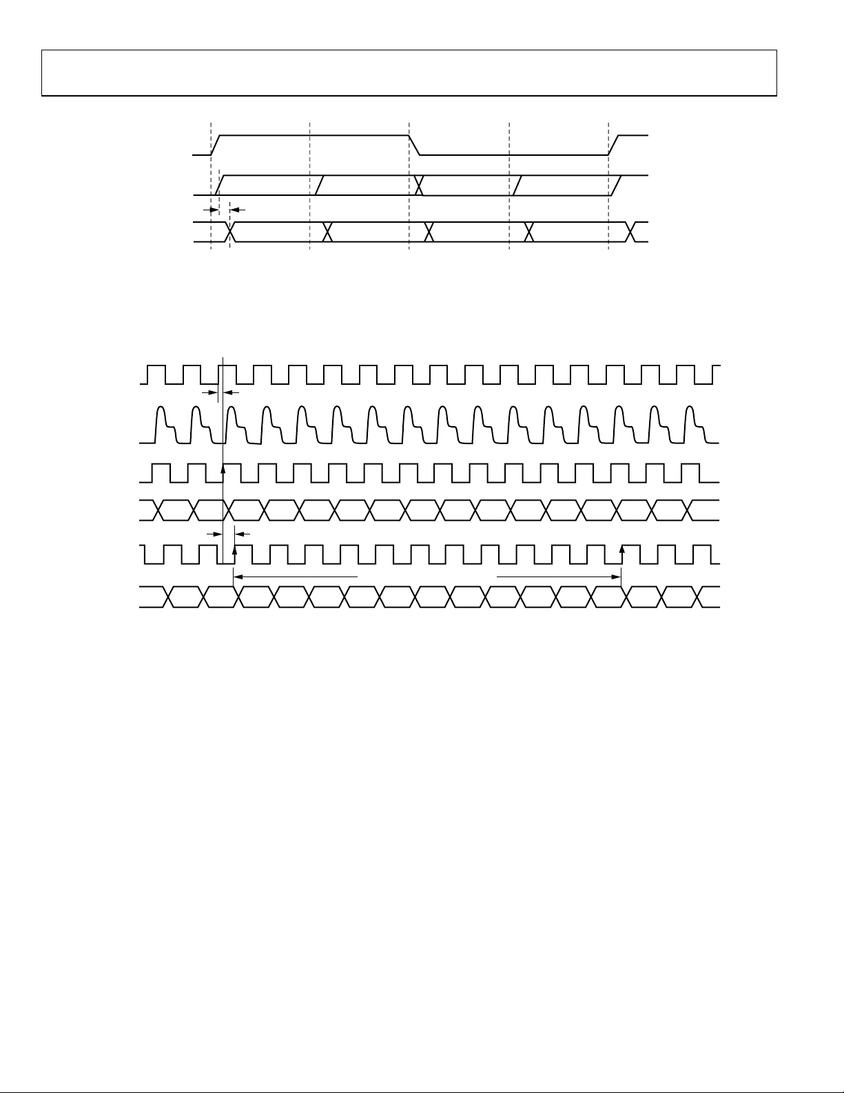
Page 30

AD9925
Generating Line Alternat
HBLK
During low resolution readout, some CCDs require a different
number of vertical clocks on alternate lines. The AD9925 can
support this by using the VPATREPO and VPATREPE registers
This allows a different number of VPAT repetitions to be programmed on odd and even lines. Note that only the number of
repeats can be different in odd and even lines, but the VPAT
group remains the same.
Additionally, the HBLK signal can also be alternated for odd
and even lines. When the HBLKALT register is set high, the
HBLK TOG1 and HBLK TOG2 positions will be used on odd
lines, and the HBLK TOG3 to HBLK TOG6 positions will be
used on even lines. This allows the HBLK interval to be adjusted
on odd and even lines if needed.
Figure 38 shows an example of a VPAT repetition alternation
and a HBLK alter
nation used together. It is also possible to use
the VPAT and HBLK alternation separately.
HD
XV1
ion for Vertical Sequence and
VPATREPO = 2
VPATREPE = 5
Second Vertical P
Most CCDs require additional vertical timing during the senso
attern Group during VSG Active Line
r
gate (SG) line. The AD9925 supports the option to output a
second vertical pattern group for XV1 to XV8 during the line
.
when the sensor gates XSG1 to XSG6 are active. Figure 39 shows
a typical SG line that includes two separate sets of vertical pattern
group for XV1 to XV6. The vertical pattern group at the start of
the SG line is selected in the same manner as the other regions,
using the appropriate VSEQSEL register. The second vertical
pattern group, unique to the SG line, is selected using the
VPATSECOND register, located with the field registers. The
start position of the second VPAT group uses the VPATLEN
register from the selected VPAT registers. Because the VPATLE
register is used as the start position and not as the VPAT lengt
it is not possible to program multiple repet
itions for the second
N
h,
VPAT group.
VPATREPO = 2
XV2
XV6
TOG1 TOG2
HBLK
NOTES
1. THE NUMBER OF REPEATS FOR THE VERTICAL PATTERN GROUP MAY B
2. THE HBLK TOGGLE POSITIONS MAY BE ALTERNATED BETWEEN ODD AN
GENERATE DIFFERENT HBLK PATTERNS FOR ODD/EVEN LINES.
Figure 38. Odd/Even Line Alteration of VPAT Repetitions and HBLK Toggle Positions
HD
XSG
XV1
XV2
TOG3
START POSITION F
USES VPATLEN RE
E ALTERN
ATED ON ODD AND EVEN LINES.
D EVEN LI
NES, IN ORDER TO
OR SECOND VPAT GROUP
GISTER
TOG4
TOG1 TOG2
04637-0-031
XV6
SECOND VPAT GROUP
Figure 39. Example of Second VPAT Group during Sensor Gate Line
Rev. A | Page 30 of 96
04637-0-032
Page 31

AD9925
×
Sweep Mode Operation
The AD9925 contains an additional mode of vertical timing
operation called sweep mode. This mode is used to generate a
large number of repetitive pulses that span across multiple HD
lines. One example of where this mode is needed is at the start
of the CCD readout operation. At the end of the image exposure,
but before the image is transferred by the sensor gate pulses, the
vertical interline CCD registers should be free of all charge. This
can be accomplished by quickly shifting out any charge using a
long series of pulses from the XV outputs. Depending on the
vertical resolution of the CCD, up to two or three thousand clock
cycles will be needed to shift the charge out of each vertical CCD
line. This operation will span across multiple HD line lengths.
Normally, the AD9925 vertical timing must be contained within
one HD line length, but when sweep mode is enabled, the HD
boundaries will be ignored until the region is finished. To enable
sweep mode within any region, program
gister to high.
re
Figure 40 shows an example of the sweep mode
number of vertical pulses needed depends on the vertical resolution of the CCD. The XV output signals are generated using
the vertical pattern registers (shown in Table 15). A single pulse
is created using the polarity and toggle position registers. The
number of repetitions is then programmed to match the number of vertical shifts required by the CCD. Repetitions are programmed in th
registers. This produces a pulse train of the appropriate length.
Normally, the pulse train is truncated at the end of the HD line
length, but with sweep mode enabled for this region, the HD
boundaries are ignored. In Figure 40, the sweep region occupies
23 HD lines. After the sweep mode region is completed in the
next region, normal sequence operation will resume. When usi
sweep mode, be sure to set the region boundaries to the appropriate lines (using the sequence change positions) to pre
eep operation from overlapping the next vertical sequence.
sw
e vertical sequence registers using the VPATREP
the appropriate SWEEP
operation. The
ng
vent the
Multiplier Mode
To generate very wide vertical timing pulses, a vertical region
may be configured into a multiplier region. This mode uses the
vertical pattern registers in a slightly different manner. Multiplier
mode can be used to support unusual CCD timing requirements,
such as vertical pulses that are wider than a single HD line length.
The start polarity and toggle positions are still used in the same
manner as the standard VPAT group programming, but the
VPATLEN is used differently. Instead of using the pixel counter
(HD counter) to specify the toggle position locations (VTOG1,
2, 3) of the VPAT group, the VPATLEN is multiplied with the
VTOG position to allow very long pulses to be generated. To
calculate the exact toggle position, counted in pixels after the
start position, use the following equation:
=
Because the VTOG register is multiplied by VPATLEN, the
resolution of the toggle position placement is reduced. If
VPATLEN = 4, then the toggle position accuracy will be reduc
to a 4-pixel step size, instead of a single pixel step size. Table 1
summarizes how the VPAT group registers are used in multiplier mode operation. In multiplier mode, the VPATREPO and
VPATREPE registers should always be programmed to the sam
value as the highest toggle position.
The example shown in Figure 41 illustrates this o
first toggle position is two, and the second toggle position is nine.
In nonmultiplier mode, this would cause the vertical sequence
to toggle at pixel 2 and then pixel 9 within a single HD line
ever, now toggle positions are multiplied by the VTPLEN = 4, so
the first toggle occurs at pixel count = 8, and the second toggle
occurs at pixel count = 36. Sweep mode has also been enable
to allow the toggle positions to cross the HD line boundaries.
VPATLENVTOGPositionToggleModeMultiplier
ed
peration. The
. How-
d
6
e
Table 16. Multiplier MODE Register Parameters
Register Length Range Description
MULTI 1 b High/Low High Enables Multiplier Mode.
XVPOL 1 b High/Low Starting Polarity of XV Signal in Each VPAT Group.
XVTOG1 12 b 0 to 4095 Pixel Location First Toggle Position for XV Signal in Each VPAT Group.
XVTOG2 12 b 0 to 4095 Pixel Location Second Toggle Position for XV Signal in Each VPAT Group.
XVTOG3 12 b 0 to 4095 Pixel Location Third Toggle Position for XV Signal in Each VPAT Group.
VPATLEN 10 b 0 to 1023 Pixels Used as Multiplier Factor for Toggle Position Counter.
VPATREP 12 b 0 to 4095 VPATREPE/VPATREPO Should Be Set to the Same Value as TOG2 or TOG3.
Rev. A | Page 31 of 96
Page 32

AD9925
X
X
VD
SCP 1 SCP 2
HD
V1 TO XV8
LINE 0 LINE 1
REGION 0 REGION 2
REGION 1: SWEEP REGION
LINE 24 LINE 25LINE 2
04637-0-033
Figure 40. Example of Sweep Region for High Speed Vertical Shift
START POSITION OF VPAT GROUP IS STILL PROGRAMMED IN THE VERTICAL SEQUENCE REGISTERS
HD
VPATLEN
PIXEL
NUMBER
V1 TO XV8
3
1234123412341234
123456789101112131415161
4
1
MULTIPLIER MODE VERTICAL PATTERN GROUP PROPER
1. START POLARITY (ABOVE: STARTPOL =
2. FIRST, SECOND, AND THIRD TOGGLE PO
3. LENGTH OF VPAT COUNTER (ABOVE: VPATLEN = 4); THI
4. TOGGLE POSITIONS OCCUR AT LOCATION EQUAL TO (VT
5. IF SWEEP REGION IS ENABLED, THE VERTICAL PULSES M
2
0).
SITIONS (ABOVE: VTOG1 = 2
5
TIES:
iplier Region
1234
71819202122232425262728293031323334353637383940
S IS THE MIN
OG × VPAT
AY ALSO C
12341234123412341234
, VTOG2 = 9).
IMUM RESOLUTION FOR TOGGLE POSITION CHANGES.
LEN).
ROSS THE HD BOUNDRIES, AS SHOWN ABOVE.
for Wide Vertical Pulse Timing Figure 41. Example of Mult
5
4
2
04637-0-034
Vertical Sensor Gate (Shift Gate) Patterns
an interline CCD, the sensor gates (SG) are used to transfer
In
the pixel charges from the light-sensitive image area into the
light-shielded ve l registers. From he light-shielded vertical
registers, the image
vertical transfe es in conjunction with the high ed hori-
rtica t
is then clocked out line-by-line, using the
r puls spe
zontal clocks.
Table 17 con
AD9925 has six
ns the he iste
tai summary of t
SG o o XSG6. E the o
utputs, XSG1 t
SG pattern reg
ach of
rs. The
utputs
can be assigned to one of four programmed patterns by using
the SGPATSEL registers. Each pattern is generated in a similar
manner as the vertical pattern groups, with a programmable
start polarity (SGPOL), first toggle position (SGTOG1), and
second toggle position (SGTOG2). The active line where the SG
pulses occur is programmable using the SGLINE1 and
SGLINE2 registers. Additionally, any of the XSG1 to XSG6
outputs may be individually disabled by using the SGMASK
register. The individual masking allows all of the SG patterns to
be preprogram ed, and the a opriate pulses r the differe
m ppr fo nt
fields can be separately enabled. For maximum flexibility, the
SGPATSEL, SG ASK, and SG INE registers are separately
programma or each field e the Comp Field: Comb
ing Vertical ences sectio or more deta
Additionally, t re is a register n Bank 1 (Add 0x55) that over
M L
ble f . Se lete in-
Sequ n f ils.
he i r rides the SG masking in the field registers (Bank 2). The
SGMASK_OVR register allows sensor gate masking to be
changed without modifying the field register values. Setting the
SGMASKOVR_EN bit high enables the SGMASK override
function. The SGMASK_OVR register is SCK updated, so the
new SG masking values will update immediately.
Rev. A | Page 32 of 96
Page 33

AD9925
X
Table 17. SG Pattern Registers (Also See Field Registers in Table 15)
Register Length Range Description
SGPOL 1 b High/Low Sensor Gate Starting Polarity for SG Pattern 0 to 3
SGTOG1 12 b 0 to 4095 Pixel Location First Toggle Position for SG Pattern 0 to 3
SGTOG2 12 b 0 to 4095 Pixel Location Second Toggle Position for SG Pattern 0 to 3
SGMASK_OVR 6 b Six Individual Bits SG Masking, Overrides the Values in the Field Registers
SGMASKOVR_EN 1 b Disable/Enable 1: Enables SGMASK Fast Update
VD
4
HD
12
SG PATTERNS
PROGRAMMABLE SETTINGS FOR EACH PATTERN:
1. START POLARITY OF PULSE.
2. FIRST TOGGLE POSITION.
3. SECOND TOGGLE POSITION.
4. ACTIVE LINE FOR XSG PULSES WITHIN THE FIELD (PROGRAMMABLE IN THE FIELD REGISTER, NOT FOR EACH PATTERN).
Figure 42. Vertical Sensor Ga
te Pulse Placement
3
04637-0-035
MODE Register
The MODE register is a single register that selects the field timing
of the AD9925. Typically, all the field, vertical sequence, and vertical pattern group information is programmed into the AD9925
at startup. During operation, the MODE register allows the use
select any combination of field timing to meet the current requir
r to
ements of the system. The advantage of using the MODE register in
conjunction with preprogrammed timing is that it greatly reduce
s
the system programming requirements during camera operation.
Only a few register writes are required when the camera operating
mode is changed
, rather than having to write in all the vertical
timing information with each camera mode change.
A basic still camera application might require five different fiel
ds
of vertical timing: one for draft mode operation, one for autofocusing, and three for still image readout. All of the register
timing information for the five fields would be loaded at startup.
Then, during camera operation, the MODE register would select
which field timing would be active depending on how the camer
was being used. Table 18 shows how the MODE register data
bits are used. The three MSBs, D23 to D21, are used to specify
how many total fields will be used. Any value from 1 to 7 can be
selected using t
hese three bits. The remaining register bits are
divided into 3-bit sections to select which of the six fields ar
used and in which order. Up to seven fields may be used in a
single MODE write. The AD9925 will start with the field timin
specified by the first field bits, and on the next VD it will switch
to the timing specified by the second field bits, and so on.
After completing the total number of fields specified in Bits D23
to D21, the AD9925 will repeat by starting at the first field again
This will continue
Figure 43 shows examples of the MODE regis
until a new write to the MODE register occurs.
ter settings for
different field configurations.
Table 18. MODE Register Data Bit Breakdown (D23 = MSB)
D23 D22 D21 D20 D19 D18 D17 D16 D15 D14 D1
3 D12 D11 D10 D9 D8 D7 D6 D5 D4 D3 D2 D1 D0
Total Number of
Fields to Use Seventh Field Sixth Field Fifth Field Fourth Field Third Field Second Field First Field
1 = First Field Only 0 = Field 0 0 = Field 0 0 = Field 0 0 = Field 0 0 = Field 0 0 = Field 0 0 = Field 0
7 = All 7 Fields 5 = Field 5 5 = Field 5 5 = Field 5 5 = Field 5 5 = Field 5 5 = Field 5 5 = Field 5
0 = Invalid 6, 7 = Invalid 6, 7 = Invalid 6, 7 = Invalid 6, 7 = Invalid 6, 7 = Invalid 6, 7 = Invalid 6, 7 = Invalid
a
e
g
.
Rev. A | Page 33 of 96
Page 34

AD9925
EXAMPLE 1:
TOTAL FIELDS = 3, FIRST FIELD = FIELD 0, SECOND FIELD = FIELD 1, THIRD FIELD = FIELD 2
MODE REGISTER CONTENTS = 0x60 0088
FIELD 0
EXAMPLE 2:
TOTAL FIELDS = 2, FIRST FIELD = FIELD 3, SECOND
MODE REGISTER CONTENTS = 0x40 0023
FIELD 3
LE 3:
EXAMP
TOTAL FIELDS = 4, FIRST FIELD = FIELD 5, SECO
MODE REGISTER CONTENTS = 0x80 050D
FIELD 5
FIELD 1 FIELD 2
FIELD 4
FIELD 1 FIELD 4
Figure 43. Using the M
VERTICAL TIMING EXAMPLE
To better understand how the AD9925 vertical timing generatio
is used, consider CCD timing chart in Figure 44. This partic
example illustrates a CCD using a general 3-field readout technique. As described in the previous field section, each readout
field should be divided into separate regions to perform each
step of the readout. The sequence change positions (SCP)
determine the line boundaries for each region, and then the
SEQSEL registers assign a particular vertical sequence to each
V
egion. The vertical sequences contain the specific timing
r
formation required in each region: XV1 to XV6 pulses (using
in
PAT groups), HBLK/CLPOB timing, and XSG patterns for the
V
SG active lines.
This particular timing example requires four regions for each of
the three fields, labeled Region 0, Region 1, Region 2, and
Region 3. Because the AD9925 allows up to six individual fields
to be programmed, the Field 0, Field 1, and Field 2 registers can
be used to meet the requirements of this timing example. The
four regions for each field are very similar in this example, but
the individual registers for each field allow flexibility to accommodate other timing charts.
Region 0 is a high speed vertical shift region. Sweep mode may
be used to generate this timing operation, with the desired
n
ular
FIELD = FI
ND FIELD = FI
FIELD 2
ODE Regist
ELD 4
ELD 1, THIRD FIELD = FIELD 4, FOURTH FIELD = FIELD 2
04637-0-036
er to Select Field Timing
number of high speed vertical pulses needed to clear any char
from the CCD’s vertical registers. Region 1 consists of only tw
lines and, like Region 3, uses standard single line vertical shift
timing. Region 2 is the sensor gate line, where the VSG pulses
transfer the image into the vertical CCD registers. This region
may require the use of the second vertical pattern group for the
SG active line.
In summary, four regions are required in each of the three
fields. The timing for Region 1 and Region 3 is essentially the
same, reducing the complexity of the register programming.
However, other registers will need to be used during the actual
readout operation, such as the MODE register, shutter control
registers (TRIGG
nd the AFE gain register. These registers will be explained in
a
ER, SUBCK, VSUB, MSHUT, and STROBE),
other examples.
Important Note about Signal Polarities
When programming the AD9925 to generate the XV1 to XV8,
XSG1 to XSG6, and SUBCK signals, it is important to note that
the vertical driver circuit will invert these signals. Carefully
check the required timing signals needed at the output of the
vertical driver circuit and adjust the polarities of the XV signals
accordingly.
ge
o
Rev. A | Page 34 of 96
Page 35

AD9925
OPEN
N
N–3
21
18
15
12
9
6
3
REGION 1 REGION 2
REGION 0 REGION 3REGION 0
THIRD FIELD READOUT
N–1
N–4
20
17
14
11
8
5
2
REGION 3
ECOND FIE D READOUT
S L
) FIRST FIELD READOUT
EXP
EXPOSURE (t
CLOSED
OPEN
FIELD 1 FIELD 2
REGION 1 REGION 2
N–2
N–5
16
13
10
7
4
1
FIELD 0
REGION 1 REGION 2
REGION 0 REGION 3
VD
HD
V1
V3
V2
V4
V6
SUBCK
MSHUT
VSUB
CCD
V5
OUT
04637-0-037
Figure 44. CCD Timing Example—Dividing Each Field into Regions
Rev. A | Page 35 of 96
Page 36

AD9925
SHUTTER TIMING C
The CCD image exposure time is controlled by the substrate
clock signal (SUBCK), which pulses the CCD substrate to clear
out accumulated charge. The AD9925 supports three types of
electronic shuttering: normal, high precision, and low speed.
Along with the SUBCK pulse placement, the AD9925
commodate different readou
the SUBCK pulses during multiple field readouts. The AD9925
also provides programmable outputs to control an external
chanical shutter (MSHUT), a strobe/flash (STROBE), and the
CCD bias select signal (VSUB).
Normal Shutter Operation
By default, the AD9925 always op
configuration, in which the SUBCK signal pulses in every VD
field (see Figure 45). The SUBCK pulse occurs once per line,
and the total number of repetitions within the field will determine the length of the exposure time. The SUBCK pulse polarity and toggle positions within a line are programmable using
the SUBCKPOL and SUBCK1TOG registers (see Table 19). The
number of SUBCK pulses per field is programmed in the
SUBCKNUM register (Addr 0x63).
As shown in Figure 45, the SUBCK pulses will always begin
in the line following the SG active line, which is specified
in the SGACTLINE registers for each f
SUBCK1TOG, SUBCK2TOG, SUBCKNUM, and SUBCKSUPPRESS registers are updated at the start of the line after the sensor
gate line, as described in the Updating New Register V
ONTROL
can ac-
t configurations to further suppress
me-
erates in the normal shutter
ield. The SUBCKPOL,
alues section.
High Precision Shutter Operation
High precision shuttering is used in the same manner as norma
shuttering, but it uses an additional register to control the last
SUBCK pulse. In this mode, the SUBCK still pulses once per
line, but the last SUBCK in the field will have an additional
SUBCK pulse, the location of which is determined by the
SUBCK2TOG register, as shown in Figure 46. Finer resolution
of the exposure time is possible using this mode. Leaving the
SUBCK2TOG register set to its maximum value (0xFF FF
FF)
will disable the last SUBCK pulse (default setting).
Low Speed Shutter Op
Normal and high
eration
precision shutter operations are used when
the exposure time is less than one field long. For exposure time
longer than one field interval, low speed shutter operation is
used. The AD9925 uses a separate exposure counter to achieve
long exposure times. The number of fields for the low speed
shutter operation is specified in the EXPOSURE register
(Addr 0x62). As shown in Figure 47, this shutter mode will
suppress the SUBCK and VSG outputs for up to 4095 fields (VD
periods). The V
D and HD outputs may be suppressed during the
exposure period by programming the VDHDOFF register to 1.
To generate a low speed shutter operation, it is necessary to
trigger the start of the long exposure by writing to the TRIGGE
Register Bit D3. When
the AD9925 will begin an exposu
this bit is set high, at the next VD edge,
re operation. If a value greater
R
than 0 is specified in the EXPOSURE register, AD9925 will
suppress the SUBCK output on subsequent fields.
If the exposure is generated using the TRIGGER register and
the EXPOSURE register is set to 0, then the behavior of the
SUBCK will not be any different than that of normal shutter o
r
high precision shutter operations, in which the TRIGGER register is not used.
l
s
VD
HD
XSG
SUBCK
SUBCK PROGRAMMABLE SETTINGS:
1. PULSE POLARITY USING THE SUBCKPOL REGISTER.
2. NUMBER OF PULSES WITHIN THE FIELD USING THE SUBCKNUM REGISTER (SUBNUM = 3 IN THE ABOVE EXAMPLE).
3. PIXEL LOCATION OF PULSE WITHIN THE LINE AND PULSE WIDTH PROGRAMMED USING SUBCK1 TOGGLE POSITION REGISTER.
t
EXP
Figure 45. Normal Shutter Mode
t
EXP
04637-0-038
Rev. A | Page 36 of 96
Page 37

AD9925
S
VD
HD
XSG
UBCK
NOTES
1. SECOND SUBCK PULSE IS ADDED IN THE LAST SUBCK LINE.
2. LOCATION OF SECOND PULSE IS FULLY PROGRAMMABLE USING THE SUBCK2 TOGGLE POSITION REGISTER.
t
EXP
t
EXP
04637-0-039
Figure 46. High Precision Shutter Mode
TRIGGER
EXPOSURE
VD
XSG
t
EXP
SUBCK
NOTES
1. SUBCK MAY BE SUPPRESSED FOR MULTIPLE FIELDS BY PROG
2. ABOVE EXAMPLE USES EXPOSURE = 1.
3. TRIGGER REGISTER MUST ALSO BE USED TO START THE LOW
4. VD/HD OUTPUTS MAY ALSO BE SUPPRESSED USING THE VDH
RAMMING T
SPEED EXP
DOFF REGIS
utter Mode
HE EXPOSURE REGISTER GREATER THAN ZERO.
OSURE.
TER = 1.
Using EXPOSURE Register Figure 47. Low Speed Sh
04637-0-040
Table 19. Shutter MODE Register Parameters
Register Length Range D
TRIGGER 5 b On/Off for Five Signals
escription
Trigger for VSUB [0], MSHUT [1], STROBE [2],
Exposure [3], and Readout Start [4]
READOUT 3 b 0 to 7 Number of Fields Number of Fields to Suppress SUBCK after Exposure
EXPOSURE 12 b 0 to 4095 Number of Fields
Number of Fields to Suppress to SUBCK and VSG
during Exposure Time (Low Speed Shutter)
VDHDOFF 1 b On/Off Disable VD/HD Output during Exposure (1 = On, 0 = Off)
SUBCKPOL1 1 b High/Low SUBCK Start Polarity for SUBCK1 and SUBCK2
SUBCK1TOG1 24 b 0 to 4095 Pixel Loca BCK Pulse (Normal Shutter) tions Toggle Positions for First SU
SUBCK2TOG1 24 b 0 to 4095 Pixel Locations Toggle Positions for Second SUBCK Pulse in Last Line (High Precision)
SUBCKNUM1 12 b 1 to 4095 Number of Pulses Total Number of SUBCKs per Field, at 1 Pulse per Line
SUBCKSUPPRESS1 12 b 0 to 4095 Number of Pulses Number of Lines to Further Suppress SUBCK after the VSG Line
1
Register is not VD upda t is up tart of the line after the ted, bu dated at the s sensor gate line.
Rev. A | Page 37 of 96
Page 38

AD9925
SUBCK Suppression
Normally, the S Ks wil gin to pulse on the line fol g
the sensor gate lin VSG). th some CCDs, the SUBCK pu e
needs to be supp ed for or more lines following th
line. The SUBCKSUPPRES gister allows for the suppression
f the SUBCK pulses for lines following the VSG line.
o
Readout after Exposure
After the exposure, the readout of the CCD data occurs, beginning with the sensor gate (VSG) operation. By default, the
AD9925 is generating the VSG pulses in every field. In the case
where only a single exposure and a single readout frame is
needed, such as the CCD’s preview mode, the VSG and SUBCK
pulses can operate in every field.
However, in many cases, during readout, the SUBCK output
needs to be further suppressed until the readout is completed.
The READOUT register specifies the number of additional
fields after the exposure to continue the suppression of SUBCK.
READOUT can be programmed for zero to seven additional
fields and should be preprogrammed at startup, not at the same
time as the exposure write. A typical interlaced CCD frame
readout mode will generally require two additional fields of
SUBCK suppression (READOUT = 2). A 3-field, 6-phase CCD
will require three additional fields of SUBCK suppression after
the readout begins (READOUT = 3).
If the SUBCK output is required to start back up during the last
field of readout, simply program the READOUT register to one
less than the total number of CCD readout fields.
Like the exposure operation, the readout operation must be
triggered using the TRIGGER register.
Using the TRIGGER Register
As described above, by default, the AD9925 will output the
SUBCK and VSG signals on every field. This works well for
continuous single-field exposure and readout operations, such
as the CCD’s live preview mode. However, if the CCD requires a
longer exposure time, or if multiple readout fields are needed,
the TRIGGER register needs to initiate specific exposure and
readout sequences.
Typically, the exposure and readout bits in the TRIGGER register are used together. This will initiate a complete exposure-plus
readout operation. Once the exposure has been completed, the
readout will automatically occur. The values in the EXPOSURE
and READOUT registers will determine the length of each
operation.
UBC l be lowin
e ( Wi ls
ress one e VSG
S re
It is possible to independently trigger the readout operation
without triggering the exposure operation. This w
readout to occur at th
suppressed according to the value of the READOU
The TRIGGER regist
MSHUT, and VSUB signal transitions. Each of these signals is
individually controlled, although they will be dependent on the
triggering of the exposure and readout operation.
See Figure 49 for a complete example of triggering the exposure
and readout operations.
e next VD, and the SUBCK output will be
er is also used to control the STROBE,
ill cause the
T register.
VSUB Control
The CCD readout bias (VSUB) can be programmed to accommodate different CCDs. Figure 48 shows two different modes
that are available. In Mode 0, VSUB goes active during the field
of the last SUBCK when the exposure begins. The on position
(rising edge in Figure 48) is programmable to any line within
the field. VSUB will remain active until the end of the image
readout. In Mode 1, the VSUB is not activated until the start of
the readout.
An additional function called VSUB keep-on is also available.
When this bit is set high, the VSUB output will remain on (active)
even after the readout has finished. To disable the VSUB, set
this bit back to low.
MSHUT and STROBE Control
MSHUT and STROBE operation is shown in Figure 49, Figure
50, and Figure 51. Table 20 shows the registers parameters for
controlling the MSHUT and STROBE outputs. The MSHUT
output is switched on with the MSHUTON registers, and it will
remain on until the location specified in the MSHUTOFF is
reached. The location of MSHUTOFF is fully programmable to
anywhere within the exposure period, using the FD (field), LN
(line), and PX (pixel) registers. The STROBE pulse is defined by
the on and off positions. STROBON_FD is the field in which
the STROBE is turned on, measured from the field containing
the last SUBCK before exposure begins. The STROBON_ LN
PX register gives the line and pixel positions with respect to
STROBON_FD. The STROBE off position is programmable to
any field, line, and pixel location with respect to the field of the
last SUBCK.
Rev. A | Page 38 of 96
Page 39

AD9925
TRIGGER
VSUB
VD
XSG
t
EXP
SUBCK
2
VSUB
1
VSUB OPERATION:
1. ACTIVE POLARITY IS POLARITY (ABOVE EXAMPLE IS VSUB ACTIVE HIGH).
2. ON-POSITION IS PROGRAMMABLE, MODE 0 TURNS ON AT THE START OF EXPOSURE, MODE 1 TURNS ON AT THE START OF READOUT.
3. OFF-POSITION OCCURS AT END OF READOUT.
4. OPTIONAL VSUB KEEP-ON MODE WILL LEAVE THE VSUB ACTIVE AT THE END OF READOUT.
MODE 0
2
MODE 1
READOUT
4
3
04637-0-041
Figure 48. VSUB Programmability
TRIGGER
EXPOSURE
AND MSHUT
VD
XSG
SUBCK
MSHUT
2
1
MSHUT PROGRAMMABLE SETTINGS:
1. ACTIVE POLARITY.
2. ON-POSITION IS VD UPDATED AND MAY BE SWITCHED ON AT ANY TIME.
3. OFF-POSITION CAN BE PROGRAMMED ANYWHERE FROM THE FIELD OF LAST SUBCK UNTIL THE FIELD BEFORE READOUT.
Figure 49. MSHUT Output Programmability
TRIGGER Register Limitations
Although the TRIGGER register can be used to perform a complete exposure and readout operation, there are limitations on
its use.
Once an exposure-plus readout operation has been triggered,
another exposure/readout operation cannot be triggered right
away. There must be at least one idle field (VD intervals) before
the next exposure/readout can be triggered. The same limitation applies to the triggering of the MSHUT signal. There
must be at least one idle field after the completion of the
MSHUT OFF operation before another MSHUT OFF operation can be programmed.
t
EXP
3
04637-0-042
The VSUB trigger requires two idle fields between exposure/readout operations in order to ensure proper VSUB on/off
triggering. If the VSUB signal is not required to be turned on
and off in between each successive exposure/readout operation,
then this limitation can be ignored. Using the VSUB keep-on
mode is useful when successive exposure/readout operations
are required.
Rev. A | Page 39 of 96
Page 40

AD9925
TRIGGER
EXPOSURE
AND STROBE
VD
XSG
t
EXP
SUBCK
STROBE
1
STROBE PROGRAMMABLE SETTINGS:
1. ACTIVE POLARITY.
2. ON-POSITION IS PROGRAMMABLE IN ANY FIELD DURING THE EXPOSURE TIME (WITH RESPECT TO THE FIELD CONTAINING THE LAST SUBCK).
3. OFF-POSITION IS PROGRAMMABLE IN ANY FIELD DURING THE EXPOSURE TIME
2
3
.
04637-0-043
mmability Figure 50. STROBE Output Progra
Table 20. VSUB, MSHUT, and STROBE Register Parameters
Register Length Range Description
VSUBMODE[0] 1 b High/Low VSUB Mode (0 = Mode 0, 1 = Mode 1) (See Figure 44).
VSUBMODE[1] 1 b High/Low VSUB Keep-On Mode. VSUB will stay active after readout when set high.
VSUBON[11:0] 12 b 0 to 4095 Line Location VSUB On Position. Active starting in any line of field.
VSUBON[12] 1 b High/Low VSUB Active Polarity.
MSHUTPOL[0] 1 b High/Low MSHUT Active Polarity.
MSH MSHUT Manual Enable (1 = Active or Open). UTPOL[1] 1 b On/Off
MSHUTON 24 b 0 to 4095 Line/Pixel Location MSHUT On Position Line [11:0] and Pixel [23:12] Location.
MSHUTOFF_FD 12 b 0 to 4095 Field Location Field Location to Switch Off MSHUT (Inactive or Closed).
MSHUTOFF_LNPX 24 b 0 to 4095 Line/Pixel Location Line/Pixel Position to Switch Off MSHUT (Inactive or Closed).
STROBPOL 1 b High/Low STROBE Active Polarity.
STROBON_FD 12 b 0 to 4095 Field Location STROBE ON Field Location, with Respect to Last SUBCK Field.
STROBON_LNPX 24 b 0 to 4095 Line/Pixel Location STROBE ON Line/Pixel Position.
STROBOFF_FD 12 b 0 to 4095 Field Location STROBE OFF Field Location, with Respect to Last SUBCK Field.
STROBOFF_LNPX 24 b 0 to 4095 Line/Pixel Location STROBE OFF Line/Pixel Position.
Rev. A | Page 40 of 96
Page 41

AD9925
EXAMPLE OF EXPO RLACED FRAME
SURE AND READOUT OF INTE
OPEN
10
810
STILL IMAGE READOUT
10
10
DRAFT IMAGEDRAFT IMAGE
67
5
EXP
t
4
2
1 9
SERIAL
WRITES
VD
XSG
SUBCK
STROBE
MSHUT
CLOSED
OPEN
SHUTTER
MECHANICAL
STILL IMAGE FIRST FIELD STILL IMAGE THIRD FIELDSTILL IMAGE SECOND FIELD
MODE 1
MODE 0
3
CCD
VSUB
DRAFT IMAGE
OUT
04637-0-044
Figure 51. Example of Exposure and Still Image Readout Using Shutter Signals and MODE Register
Rev. A | Page 41 of 96
Page 42

AD9925
Refer to Figure 51 for each step:
1. Write to the READOUT register (Addr x61) to specify the
number of fields to further suppress SUBCK while the
CCD data is readout. In this example, READOUT = 3.
Write to the EXPOSURE register (Addr x62) to specify the
number of fields to suppress SUBCK and VSG outputs during exposure. In this example, EXPOSURE = 1.
Write to the TRIGGER register (Addr x60) to enable the
STROBE, MSHUT, and VSUB signals and to st
posure/readout operation. To trigger these events (as in
Figure 56), set the register TRIGGER = 31. Readout will
automatically occur after the exposure period is finished.
Write to the MODE register (x1B) to configure the next
five fields. The first two fie
same as the current draft mode fields, and the following
three fields are the still frame readout fields. The registers
for the draft mode field and the three readout fields have
already been programmed.
2. The VD/HD falling edge will update the serial writes from 1.
3. If VSUB mode = 0 (Addr x67), VSUB output will turn on at
the line specified in the VSUBON register (Addr x68).
lds during exposure are the
art the ex-
4. STROBE output turns on and off at the location specified
in the STROBEON and STROBEOFF registers (Addr x6E
to x71).
5. MSHUT output turns off at the location specified in the
MSHUTOFF registers (Addr x6B and x6C).
6. The next VD falling edge will automatically start the first
readout field.
7. The next VD falling edge will automatically s art the sec-
ond readout field.
8. The next VD falling edge will automatically start the third
readout field.
9. Write to the MODE register to reconfigure the single draft
mode field timing. Write to the MSHUTON register
(Addr x6A) to open the mech
10. VD/HD falling edge will update the serial writes from 9.
VSG outputs return to draft mode timing.
SUBCK output resumes operation.
MSHUT output returns to the on position (active or open).
VSUB output returns to the off position (inactive).
anical shutter.
t
Rev. A | Page 42 of 96
Page 43

AD9925
FG_TRIG OPERATION
The AD9925 contains an additional signal that may be used in
conjunction with shutter operation or general system operation.
The FG_TRIG signal is an internally generated pulse that can be
output on the VSUB or SYNC pins for system use or combined
with the VSUB registers to create a four-toggle VSUB signal.
The FG_TRIG signal is generated using the start polarity and
first and second toggle position registers, programmable with
line and pixel resolution. The field placement of the FG_TRIG
pulse is matched to the field count specified by the MODE register operation. The FG_TRIGEN register contains a 3-bit value
to specify which field count will contain the FG_TRIG pulse.
Figure 53 shows how the FG_TRIG pulse is generated using
these registers.
One final application for the FG_TRIG signal is to combine it
with the existing VSUB signal to generate additional toggle
positions. By setting the SHUT_EXTRA Bit 8 to a 1, the VSUB
toggles and FG_TRIG toggles are XOR’d together and sent to the
VSUB output. Figure 52 and Figure 54 show this application in
more detail.
FG_TRIG
INTERNAL
XOR
VSUB
INTERNAL
Figure 52. Combining the Internal FG_TRIG and Internal VSUB Signals
1
2:1
0
SHUT_EXTRA[8]
1
2:1
0
SHUT_EXTRA[3]
VSUB
OUTPUT
04637-0-074
After the FG_TRIG signal is specified, it is enabled using Bit 3
of the FG_TRIGEN register. By default, the FG_TRIG will be
mapped to the SYNC output, as long as the SYNC pin is configured as an output (SYNCENABLE = 1). Alternatively, the
FG_TRIG pulse may be mapped to the VSUB output by
writing a 1 to the SHUT_EXTRA Register Bit 3.
Table 21. FG_TRIG Operation Registers
scription Register Address Bit Width De
SYNCENABLE 0x12 [0] 1: Configures SYNC Pin as an Output. By default, the FG_TRIG signal outputs on the SYNC pin.
VSUBON 0x68 [12:0]
SHUT_EXTRA 0xE7 [8:0]
Controls VSUB O
with VSUB signa
n Position and
l.
Selects Whether FG_TRIG Sign
Polarity. When SHUT_Extra [8] = 1, FG_TRIG toggles are combined
al Is Used with VSUB.
[2:0] Set to 0.
[3] Set = 1 to send FG_TRIG signal to VSUB pin.
[7:4] Set to 0.
bine FG_TRI
count for pulse d counter).
le FG_TRIG sign
(based on mode fiel
al output.
FG_TRIGEN 0xEB [3:0]
[8] Set = 1 to com G and VSUB signals.
FG_TRIG Enable.
[2:0] Selects field
[3] Set = 1 to enab
FG_TRIGPOL 0xF2 [0] FG_TRIG Start Polarity.
FG_TRIGLINE1 0xF3 [11:0] FG_TRIG First Toggle Position, Line Location.
FG_TRIGPIX1 0xF4 [12:0] FG_TRIG First Toggle Position, Pixel Location.
FG_TRIGLINE2 0xF5 [11:0] FG_TRIG Second Toggle Position, Line Location.
FG_TRIGPIX2 0xF6 [12:0] FG_TRIG Second Toggle Position, Pixel Location.
Rev. A | Page 43 of 96
Page 44

AD9925
VD
MODE REGISTER
FIELD COUNT
FG_TRIG 1
FIELD 0 FIELD 1
4
FG_TRIG PROGRAMMABLE SETTINGS:
1. ACTIVE POLARITY.
2. FIRST TOGGLE POSITION, LINE AND PIXEL LOCATION.
3. SECOND TOGGLE POSITION, LINE AND PIXEL LOCATION.
4. FIELD PLACEMENT BASED ON MODE REGISTER FIELD COUN
VD
VSUB
INTERNAL
FG_TRIG
INTERNAL
VSUB OUT
SHUT_XTRA[8] = 0
VSUB OUT
SHUT_XTRA[8] = 1
23
Figure 54. Combining FG_TRIG and VSUB to Create Four Toggle Positions for VSUB Output
FIELD 2 FIELD 0 FIELD 1
4
T.
G_TRIG Signal Figure 53. Generating the F
04637-0-067
04637-0-066
Rev. A | Page 44 of 96
Page 45

AD9925
1.0µF 1.0µF
REFTREFB
0.1µF
CCDIN
DC RESTORE
1.3V
SHP
CDS
SHP
SHD
DOUT
SHD
PHASE CLPOB PBLK
6dB ~ 42dB
VGA
VGA GAIN
REGISTER
DAC
1.0V 2.0V
INTERNAL
V
REF
12-BIT
ADC
OPTICAL BLACK
CLAMP
DIGITAL
FILTER
CLI
DOUT PHASE
2V FULL SCALE
CLAMP LEVEL
REGISTER
CLPOB
8
FIXED
DELAY
DOUT
DLY
OUTPUT
DATA
LATCH
PBLK
1
0
DCLK
MODE
12
DCLK
DOUT
CLI
PRECISION
TIMING
GENERATION
V-H
TIMING
GENERATION
Figure 55. Analog Front End Functional Block Diagram
ANALOG FRONT END DESCRIPTION AND OPERATION
The AD9925 signal processing chain is shown in Figure 55.
Each processing step is essential in achieving a high quality
image from the raw CCD pixel data.
DC Restore
To reduce the large dc offset of the CCD output signal, a dcrestore circuit is used with an external 0.1 µF series coupling
capacitor. This restores the dc level of the CCD signal to approximately 1.3 V, which allows it to be compatible with the
3 V supply voltage of the AD9925.
Correlated Double Sampler
he CDS circuit samples each CCD pixel twice to extract the
T
video information and reject the low frequency noise. The timing
shown in Figure 19 illustrates how the two internally generated
CDS clocks, SHP and SHD, are used to sample the reference level
and data level of the CCD signal, respectively. The placement of
the SHP and SHD sampling edges is determined by setting the
SAMPCONTROL register located at Addr 0x36. Placement of
these two clock signals is critical in achieving the best performance from the CCD.
AD9925
04637-A-002
Variable Gain Amplifier
The VGA stage provides a gain range of 6 dB to 42 dB, programmable with 10-bit resolution through the serial digital interface.
The minimum gain of 6 dB is needed to match a 1 V input signal
with the ADC full-scale range of 2 V. When compared to 1 V fullscale systems, the equivalent gain range is 0 dB to 36 dB.
The VGA gain curve follows a linear-in-dB characteristic. The
exact VGA gain can be calculated for any gain register value by
using the equation
Gain (dB) = (0.0351 × Code) + 6 dB
where the Code r
42
36
30
24
VGA GAIN (dB)
18
ange is 0 to 1023.
Rev. A | Page 45 of 96
12
6
0 127 255 383 511 639 767 895 1023
VGA GAIN REGISTER CODE
Figure 56. VGA Gain Curve
04637-0-046
Page 46

AD9925
ADC
The AD992 rmance ADC architecture, optimized fo eed and erential nonl
(D ce
NL) performan is typically better than 0.5 LSB. The ADC
uses a 2 V in ange re 12
typical linearit nd noise performanc s for the
for y a e plot
9925.
AD
ptical Black Clamp
O
The optical black clamp loop is
in the signa low frequency variations in the
CCD’s black l . During k (shielded) p
val on each lin e ADC output is com d with a fixed
ter e, th pare
black le ce, s in the
reg twee
ister. The value can be programmed be n 0 LSB and
LSB in 256 st esulting error iltered to
255 eps. The r signal is f
educe noise, and the correction value is applied to the ADC
r
put through a DAC. Normally, the optical black clamp loop is
in
turned on once per horizontal lin
more slowly lar application. If external digital
clamp during t g, the AD9925
black clam ay b D2 in
ister. When th p is disabled, the cla evel register may
reg e loo mp l
l be used to pr e programmable off djustment.
stil ovid set a
The CLPO g th
lack pixels. It is recommended that the CLPOB pulse duration
b
be at least 20 pixels wide. Shorter
the ability t ncy variations in the black level
will b e the H ping and Blank
tion for timing examples.
sec
5 uses high perfo
r high sp low power. Diff inearity
put r . See Figure 10, Figu , and Figure 13
used to remove residual offsets
l chain and to track
evel the optical blac ixel in-
vel referen elected by the user clamp level
e, but this loop can be updated
to suit a particu
ing is used he postprocessin optical
ping m e disabled using Bit the OPRMODE
B pulse should be placed durin e CCD’s optical
pulse widths may be used, but
o track low freque
e reduced. Se orizontal Clam ing
Digital Data Outputs
The AD9925 ta is latched using the DOUT
PHAS e, as sho . Output data t
ing is sh re 2 also
ve the output latc transparent, so that t ata outputs are
lea hes he d
d immediately fr the ADC. Programm the AFE
vali om ing
NTROL Register to a 1 will set th put latches
CO Bit D4 e out
ansparent. The data outputs can also be disabled (three stated)
tr
by setting the AFE CONTROL Reg
The switchin puts can couple noise back to the
analog o minimi ng noise, it is r
om DO be se
mended that the UT PHASE register t to the same
edg plin 12 edg
e as the SHP sam g location, or up to es after the
SH on. O oduc
P sampling locati ther settings can pr e good results,
but ex is n
OUT PHASE location not occur between the SHD sampling
D
cation and 12 edges after the SHD location. For example, if
lo
SHDLOC = 0, then DOUT PHAS
location of 12 or
the da can be left tr
ister 0x03, Bit [4].
reg
The data output coding is normally straight binary, but the
oding may be changed to gray coding by setting the AFE
c
CONTROL Register Bit D5 to a
digital output da
E register valu wn in Figure 55 im-
own in Figu 1 and Figure 22. It is possible to
ister Bit D3 to a 1.
g of the data out
signal path. T ze any switchi ec-
perimentation ecessary. It is recommended that the
E should be set to an edge
greater. If adjustable phase is not required for
ta outputs, the output latch ansparent using
1.
Rev. A | Page 46 of 96
Page 47

AD9925
VERTICAL DRIVER SIGNAL CONFIGURATION
As shown in Figure 57, XV1 to XV8, XSG1 to XSG6, and
XSUBCK are outputs from the internal AD9925 timing generator, while V1 to V8 and SUBCK are the resulting outputs from
the AD9925 vertical driver. The vertical driver performs the
mixing of the XV and XSG pulses and amplifies them to the
high voltages required for driving the CCD. Additionally, the
vertical driver outputs are inverted from the internal XV, XSG,
and SUBCK polarities configured by the AD9925 registers.
Table 22 to Table 32 describe the output polarities for these
signals vs. their input levels. Refer to these tables when determining the register settings for the desired output levels.
Figure 58 to Figure 64 show graphically the relationship between
the polarities of the XV and XSG signals and the inverted vertical driver output signals.
AD9925
INTERNAL
TIMING
GENERATOR
VERTICAL DRIVER
XV1
XSG1
XV2
XSG6
XSG2
XV3
XSG3
XSG4
XV5
XSG5
XV4
XV6
XV7
XV8
XSUBCK
+3V
+15V,–7.5V
Figure 57. AD9925 Internal V-Driver Input Signals
G11
G10
H10
K10
B8
V1
V2
B9
V3A
3-LEVEL OUTPUTS
C9
V3B
D9
V5A
E9
V5B
V4
V6
2-LEVEL OUTPUTS
V7
J9
V8
J8
SUBCK
04637-0-047
Rev. A | Page 47 of 96
Page 48

AD9925
Table 22. V1 Output Polarity
V-Driver Input
XV1 XSG1
L L VH
L H VM
H L VL
H H VL
Table 23. V2
XV2 XSG6
L L VH
L H VM
H L VL
H H VL
Output Polarity
V-Driver Input
Table 24. V3A Output Polarity
V-Driver Input
XV3 XSG2
L L VH
L H VM
H L VL
H H VL
Table 25. V3B Output Polarity
V-Driver Input
XV3 XSG3
L L VH
L H VM
H L VL
H H VL
Table 26. V4 Output Polarity
V-Driver Input
XV4
L VM
H VL
V4 Output
V1 Output
V2 Output
V3A Output
V3B Output
able 27. V5A Output Polarity
T
V-Driver Input
XV5 XSG4
L L VH
L H VM
H L VL
H H VL
V5A Output
Table 28. V5B Output Polarity
V-Driver Input
XV5 XSG5
L L VH
L H VM
H L VL
H H VL
V5B Output
Table 29. V6 Output Polarity
V-Driver Input
XV6
L VM
H VL
V6 Output
Table 30. V7 Output Polarity
nput V-Driver I
XV7
L VM
H VL
V7 Output
Table 31. V8 Output Polarity
V-Driver Input
XV8
L VM
H VL
V8 Output
Table 32. SUBCK Output Polarity
V-Driver Input
XSUBCK
L VH
H VL
SUBCK Output
Rev. A | Page 48 of 96
Page 49

AD9925
V
V3A
V
XV1
XSG1
VH
1
VM
VL
04637-0-048
Figure 58. XV1, XSG1, and V1 Output Polarities
XV2
XSG6
VH
V2
VM
VL
04637-0-049
Figure 59. XV2, XSG6, and V2 Output Polarities
XV3
XSG2
VH
VM
VL
Figure 60. XV3, XSG
2, and V3A Output Polarities
04637-0-050
XV3
XSG3
VH
3B
VM
VL
04637-0-051
Figure 61. XV3, XSG3, and V3B Output Polarities
Rev. A | Page 49 of 96
Page 50

AD9925
V5A
V
XV5
XSG4
VH
VM
VL
04637-0-052
A Output Polarities Figure 62. XV5, XSG4, and V5
XV5
XSG5
VH
5B
VM
XV4, XV6,
XV7, XV8
V4, V6,
V7, V8
VL
Output Polarities Figure 63. XV5, X SG5, and V5B
VM
VL
4, XV6, XV7, XV8 and V4, , V7, V8 Output Polarities Figure 64. XV V6
04637-0-053
04637-0-054
Rev. A | Page 50 of 96
Page 51

AD9925
V
V
V
V
V
POWER-UP AND SYNCHRONIZATION
Vertical Driver Power Supply Sequencing
The recommended Power-Up and Power-Down sequences are
shown in Figure 65 and Figure 66, respectively. As shown, the
VM1 and VM2 voltage levels should never exceed the VH1 and
VH2 voltage levels during power-up or power-down. Excessive
current will result if this requirement is not met due to a PN
junction diode turning on between the VM1/VM2 and VH
supply pins.
VH1 = VH2 = 12.0V TO 15.0V
VDVDD = DVDD = DRVDD = HVDD = RGV
0V
12
SAME TIME AS VM AND VH; LATER OR EARLIER IS OK, BUT NOT BEFORE VDD REACHES 3.0V.
DD = TCVDD = AVDD = 3.0V
VM1 = VM2 = –1.0V TO –0.5V
VL = –7.5V
04637-0-055
Figure 65. Power-Up Sequence
H1 = VH2
DVDD = DVDD = DRVDD = HVDD = RGVDD = TCVDD = AVDD = 3
21
M1 = VM2
L
SAME TIME AS VM AND VH OR EARLIER, BUT NOT AFTER VDD.
0V
04637-0-056
n Sequence Figure 66. Power-Dow
Rev. A | Page 51 of 96
Page 52

AD9925
VH1 = VH2 = 15
.0V
POWER
SUPPLIES
CLI
(INPUT)
SERIAL
WRITES
SYNC
(INPUT)
VD
(OUTPUT)
HD
(OUTPUT)
DIGITAL
OUTPUTS
VDVDD = DVDD = DR VDD = RGVDD = TCVDD = A
0V
14
VL = –7.5V
H2/H4
H1/H3, RG, DCLK
Figure 67. Recommended Power-Up Sequence and Synchronization, Master Mode
VDD = H VDD = 3V
Recommended Power-Up Sequence for Master Mode
When the AD9925 is powered up, the following sequence is
recommended (refer to Figure 67 for each step). Note that a
SYNC signal is required for master mode operation. If an external SYNC pulse is not available, it is also possible to generate an
internal SYNC pulse by writing to the SYNCPOL register, as
described in the next section.
1. Turn on power supplies for the AD9925 and apply master
clock CLI.
2. Reset the internal AD9925 registers by writing a 1 to the
SW_RESET register (Addr 0x10 in Bank 1).
3. Write to the standby mode polarity registers 0x0A to 0x0D
to set the proper polarities for the V-driver inputs, in order
to avoid damage to the CCD. See Table 35 for settings.
4. The V-driver supplies, VH and VL, can then be powered up
anytime after completing Step 3 to set the proper polarities.
5. By default, the AD9925 is in standby 3 mode. To place the
part into normal power operation, write 0x004 to the AFE
OPRMODE register (Addr 0x00 in Bank 1).
6. Write a 1 to the BANKSELECT register (Addr 0×7F)). This
will select Register Bank 2. Load Bank 2 registers with the
required VPAT group, vertical sequence, and field timing
information.
1098652
1173
12
t
SYNC
1ST FIELD
1H
CLOCKS ACTIVE WHEN OUT_CONTROL
REGISTER IS UPDATED AT VD/HD EDGE
1V
04637-0-069
7. Write a 0 to the BANKSELECT register to select Bank 1.
8. By default, the internal timing core is held in a reset state
with TGCORE_RSTB register = 0. Write a 1 to the
TGCORE_RSTB register (Addr 0x15 in Bank 1) to start the
internal timing core operation. Note: If a 2x clock is used
for the CLI input, the CLIDIVIDE register (Addr 0x30)
should be set to 1 before resetting the timing core.
9. Load the required registers to configure the high speed
timing, horizontal timing, and shutter timing information.
10. Configure the AD9925 for master mode timing by writing
a 1 to the MASTER register (Addr 0x20 in Bank 1).
11. Write a 1 to the OUT_CONTROL register (Addr 0x11 in
Bank 1).This will allow the outputs to become active after
the next SYNC rising edge.
12. Generate a SYNC event: If SYNC is high at power-up,
bring the SYNC input low for a minimum of 100 ns. Then
bring SYNC back to high. This will cause the internal
counters to reset and will start the VD/HD operation. The
first VD/HD edge allows most Bank 1 register updates to
occur, including OUT_CONTROL to enable all outputs.
Rev. A | Page 52 of 96
Page 53

AD9925
Table 33. Power-Up Register Write Sequence
Address scription
0x10 0x01 Re Registers to Default Vaset All lues
0x0A to 0x0D TBD Standby V-Driver Input Signal Polarities
0x00 0x04 Power-Up the AFE and CLO Oscillator
0x7F 0x01 Select Register Bank 2
0x00 to 0xFF TBD
0x7F 0x00 Select Register Bank 1
0x15 0x01 Reset Internal Timing Core
0x31 to 0x71 TBD Ho l and Shutter Timing rizonta
0x20 0x01 Configure for Master Mode
0x11 0x01 Enable All Outputs after SYNC
0x13 0x01 SYNCPOL (for Software SYNC Only)
Generating Software SYN out External SYNC
If an exte not av generate an i NCPO
nternal SYNC in the AD9925 by writing to the SY L
register ( softwa d, the
SYNC inp be tie
Data De
VP rtical Sequence, and Fi
AT, Ve eld
Tim
ing
C with Signal
rnal SYNC pulse is ailable, it is possible to
Addr 0x13). If the re SYNC option is use
ut (Pin J5) should d to ground (VSS).
After power-up, follow the same procedure as before, for Steps 1
through 11. Then, for Step 12, instead of using the external
SYNC pulse, write a 1 to the SYNCPOL register. This will generate the SYNC internally, and the timing operation will begin.
SYNC during Master Mode Operation
he SYNC input may be used any time during operation to
T
resync the AD9925 counters with external timing, as shown in
Figure 68. The operation of the digital outputs may be suspended
during the SYNC operation by setting the SYNCSUSPEND register (Addr 0x14) to a 1.
Power-Up and Synchronization in Slave Mode
The power-up procedure for slave mode operation is the same
as the procedure described for master mode operation, with
two exceptions:
1. Eliminate Step 10. Do not write the part into master mode.
2. No SYNC pulse is required in slave mode. Substitute Step
12 with starting the external VD and HD signals. This will
synchronize the part, allow the Bank 1 register updates,
and start the timing operation.
When the AD9925 is used in slave m
re us nize the intern ollowing a
puts a ed to synchro al counters. F
falling edg , there will be a latenc master clock edges
(CLI) after lling edge of HD until t ernal H-Counter is
reset. The r eration is shown in Fig .
Vertical T emen Counter Reset
One addit nsideration during th f the internal
counters is tical toggle position pl nt. Before the internal coun e reset, there is an area ls where no
toggle posi ould be programmed
For master the last 18 pixels befo D falling edge
should not d for toggle position pl nt of the XV, XSG,
SUBCK, H BLK, or CLPOB puls ure 70).
Figure 71 he same example for sl de. The same
restriction the last 18 pixels befo counters are reset
and canno ed. However, in slave m he counter reset is
delayed wi ect to VD/HD placem erefore, the inhibited area is nt than it is in master
e of VD y of 23
the fa he int
eset op ure 69
oggle Position Plac t near
ional co e reset o
the ver aceme
ters ar of 18 pixe
tions sh .
mode, re the H
be use aceme
BLK, P es (see Fig
shows t ave mo
applies: re the
t be us ode, t
th resp ent; th
differe mode.
Additional Considerations for Toggle Positions
In addition to avoiding toggle position placement near the counterreset location, there are a couple of other recommendations.
Pixel location 0 should not be used for any of the toggle positions
for the XSG and SUBCK pulses.
Also, the propagation delay of the V-driver circuit should be considered when programming the toggle positions for the XV, XSG,
and SUBCK pulses. The delay of the V-driver circuit is specified
in Table 3 and is a maximum of 200 ns.
ode, the VD and HD in-
Rev. A | Page 53 of 96
Page 54

AD9925
H124, RG, V1 TO 4,
SYNC
VD
HD
VSG, SUBCK
NOTES
1. SYNC RISING EDGE RESETS VD/HD AND COUNTERS TO ZERO.
2. SYNC POLARITY IS PROGRAMMABLE USING SYNCPOL REGIS
3. DURING SYNC LOW, ALL INTERNAL COUNTERS ARE RESE
4. IF SYNCSUSPEND = 1, VERTICAL CLOCKS, H1 TO H2, AND
5. IF SYNCSUSPEND = 0, CLOCK OUTPUTS CONTINUE TO OPERA
Figure 68. SYNC Timing to S
VD
SUSPEND
TER (ADDR 0
T AND VD/HD CA
RG ARE HELD A
TE NORMAL
x13).
N BE SUSPENDED USING THE SYNCSUSPEND REGISTER (ADDR 0x14).
T THEIR DEFAULT POLARITIES.
LY UNTIL SYNC RESET EDGE.
ynchronize AD9925 with External Timing
04637-0-058
HD
CLI
H-COUNTER
(PIXEL COUNTER)
H-COUNTER
(PIXEL COUNTER)
3ns MIN
XXXXXXXXX
NOTE
INTERNAL H-COUNTER IS RESET 23 CLOCK EDGES AFTER THE HD FALLING EDGE.
XXX XXXXXXXX XXXX
Figure 69. External VD/HD and Internal H-Counter Synchronization, Slave Mode
VD
HD
NO TOGGLE POSITIONS ALLOWED IN THIS AREA
NOTE
TOGGLE POSITIONS CANNOT BE PROGRAMMED WITHIN 18 PIXELS OF PIXEL 0 LOCATION.
Figure 70. Toggle Position Inhibit Area, Master Mode
VD
H-COUNTER
RESET
01234
04637-0-076
H-COUNTER
RESET
01234
N-3N-4N-5N-6N-7N-8N-9N-10N-11N-12N-13N-14N-15N-16N-17N-18N-19N-20N-21N-22
NN-1N-2
04637-0-077
HD
H-COUNTER
(PIXEL COUNTER)
NO TOGGLE POSITIONS ALLOWED IN THIS AREA
NOTE
TOGGLE POSITIONS CANNOT BE PROGRAMMED WITHIN 18 PIXELS OF PIXEL 0 LOCATION.
Figure 71. Toggle Position Inhibit Area, Slave Mode
Rev. A | Page 54 of 96
H-COUNTER
RESET
01234
N-3N-4N-5N-6N-7N-8N-9N-10N-11N-12N-13N-14N-15N-16N-17N-18N-19N-20N-21N-22
NN-1N-2
04637-0-078
Page 55

AD9925
STANDBY MODE OPERATION
The AD9925 contains three different standby modes to optimize
the overall power dissipation in a particular application. Bits [1:0]
of the OPRMODE register control the power-down state of the
device:
OPRMODE[1:0] = 00 = Normal Operation (Full Power)
OPRMODE[1:0] = 01 = Standby 1 Mode
OPRMODE[1:0] = 10 = Standby 2 Mode
OPRMODE[1:0] = 11 = Standby 3 Mode (Lowest Overall Power)
the digital output states, but the standby 3 mode takes priority
over OUT_CONTROL. Standby 3 mode has the lowest power
consumption and even shuts down the crystal oscillator circuit
between CLI and CLO. Thus, if CLI and CLO are being used
with a crystal to generate the master clock, this circuit will be
powered down and there will be no clock signal. When returning from standby 3 mode to normal operation, the timing core
must be reset at least 500 µs after the OPRMODE register is
written to. This will allow sufficient time for the crystal circuit
to settle.
Table 34 and Table 35 summarize the operation of each powerdown mode. Note that the OUT_CONTROL register takes
priority over the standby 1 and standby 2 modes in determining
The XV and shutter outputs can also be programmed to hold a
specific value during any of the standby modes, as detailed in
Table 35.
Table 34. Standby Mode Operation
I/O Block Standby 3 (Default)
1, 2
OUT_CONT= LO2 Standby 2
3, 4
Standby 1
3, 4
AFE Off No Change Off Off
Timing Core Off No Change Off Off
CLO Oscillator Off No Change On On
CLO High Running Running Running
H1 Hi-Z Low Low (4.3 mA) Low (4.3 mA)
H2 Hi-Z High High (4.3 mA) High (4.3 mA)
H3 Hi-Z Low Low (4.3 mA) Low (4.3 mA)
H4 Hi-Z High High (4.3 mA) High (4.3 mA)
RG Hi-Z Low Low (4.3 mA) Low (4.3 mA)
VD Low VDHDPOL Value VDHDPOL Value Undefined in Master Mode
HD Low VDHDPOL Value VDHDPOL Value Undefined in Master Mode
DCLK Low Low Low Running if DCLK MODE =1
DOUT Low Low Low Low
1
To exit standby 3 mode, first write a 00 to OPRMODE[1:0], then reset the timing core after ~500 µs to guarantee proper settling of the oscillator.
2
Standby 3 mode takes priority over OUT_CONTROL for determining the output polarities.
3
These polarities assume OUT_CONT = High., because OUT_CONTROL = Low takes priority over standby 1 and standby 2 modes.
4
Standby 1 and standby 2 modes will set H and RG drive strength to minimum value (4.3 mA).
Rev. A | Page 55 of 96
Page 56

AD9925
Table 35. Standby Mode Operatio ogrammable Polarities Available)
I/O Block Standby 3 (Default) OUT_CON
XV1 Low Low Low Low
XV8 Low Low Low Low
XV3 Low Low Low Low
XV7 Low Low Low Low
XV6 Low High High High
XSG6 Low High High High
XV5 Low High High High
XV4 Low High High High
XSG5 Low High High High
XSG4 Low High High High
XV2 Low High High High
XSG3 Low High High High
XSG1 Low High High High
XSG2 Low High High High
SUBCK Low High High High
VSUB Low Low Low Low
MSHUT Low Low Low Low
STROBE Low Low Low Low
1
Polarities for vertical and shutter outputs are programmable for each standby mode, using the STBYPOL registers.
2
Default register values are:
STBY3POL = Bin 00000000000000000 = 0x00
OCONTPOL = STBY2POL = STBY1POL = Bin 000011111111111000 = 0x3FF8
3
Bit assignments for programming polarity registers: (MSB) XV1, XV8, XV3, XV7, XV6, XSG6, XV5, XV4, XSG5, XSG4, XV2, XSG3, XSG1, XSG2, SUBCK, VSUB, MSHUT, and
STROBE (LSB).
n—Vertical and Shutter Outputs (Pr
1, 2
T = Lo
2
, 3
w
Standby 23 Standby 13
Rev. A | Page 56 of 96
Page 57

AD9925
04637-0-060
CIRCUIT LAYOUT INFORMATION
The AD9925 typical circuit connections are shown in Figure 73.
The PCB layout is critical in achieving good image quality from
the AD9925. All of the supply pins, particularly the AVDD,
TCVDD, RGVDD, and HVDD supplies, must be decoupled to
ground with good quality, high frequency chip capacitors. The
decoupling capacitors should be located as close as possible to
the supply pins and should have a very low impedance path to a
continuous ground plane. There should also be a 4.7 µF or larger
value bypass capacitor near each main supply—AVDD, HVDD,
DRVDD, VL, and VH—although this is not necessary for each
individual pin. In most applications, it is easier to share the
supply for RGVDD and HVDD, which may be done as long as
the individual supply pins are separately bypassed. A separate
3 V supply may also be used for DRVDD, but this supply pin
should still be decoupled to the same ground plane as the rest
the chip. A separate ground for DRVSS is not recommended.
The analog bypass pins (REFT and REFB) should also b
lly decoupled to ground as close as possible to their respective
fu
pins. The analog input (CCDIN) capacitor should also be located
close to the pin.
of
e care-
The H1 to H4 and RG traces should be designed to have low
inductance to avoid excessive distortion of the signals. Heavier
traces are recommended because of the large transient current
demand on H1 to H4 by the CCD. If possible, physically locating the AD9925 closer to the CCD will reduce the inductance
on these lines. As always, the routing path should be as direct as
possible from the AD9925 to the CCD.
The AD9925 also contains an on-chip oscillator for driving an
external crystal. Figure 72 shows an example of an application
using a typical 24 MHz crystal. For the exact values of the external resistors and capacitors, it is best to consult with the crystal
manufacturer’s data sheet.
AD9925
J6
CLI CLO
1MΩ
20pF
Figure 72. Crystal Driver Application
24MHz
XTAL
J4
500Ω
20pF
Rev. A | Page 57 of 96
Page 58

AD9925
+
DCLK TO ASIC/DSP
12
ATA
D
UTS
OUTP
3V DRIVER
+
VSUB TO CCD
HORIZONTAL SYNC TO/FROM ASIC/DSP
+3V ANALOG SUPPLY
0.1µF
–7.5V SUPPLY
+15V SUPPLY
0.1µF 0.1µF
DVSSHDVD
F9
G9
F10
TO SCALE
F1
V2V4V6V7V8
G11
G10
G1
H1H2H3J2J3J1K1
VL
VH1
E11
C6
VM1V1V3A
C7C8B8B9C9
NCNCNC
A11
DCLK
D0 (LSB)
D1
D2
D3
D4
D5
D6
D7
D8
D9
D10
D11 (MSB)
DRVDD
DRVSS
0.1µF4.7µF
0.1µF
VSUB
VDVDD
VDVSS
NC
NC
NC
NC
NC
NC
D10
E10
D11
C10
C11
B10
B11
A10
A9
A8
B7
A7
B6
A6
C5
B5
A5
A4
B4
C4
B3
A3
B2
A2
A1
B1
C1C2C3D1D2D3E2
DVDD
V3B
V5A
V5B
E9
D9
D9925
A
NOT DRAWN
E1F2F3G2G3
E3
F11
VM2
J9
K10
H10
VERTICAL SYNC TO/FROM ASIC/DSP
STROBE
SCK
SDI
H9
J11
J10
H11
K11
L11
L10
L1
SL
NC
RSTB
VH2
K9
VL
K8
SUBCK
J8
MSHUT
J7
REFB
L9
REFT
L8
AVDD
K7
CCDIN
L6
AVSS
L7
AVSS
K6
CLI
J6
TCVSS
L5
TCVSS
K5
SYNC
J5
CLO
J4
TCVDD
K4
TCVDD
K3
RGVDD
L4
RG
L3
RGVSS
L2
RGVSS
K2
10
VERTICAL CLOCK OUTPUTS
(TO CCD)
TO STROBE CIRCUIT
3
SERIAL INTERFACE
(FROM ASIC/DSP)
EXTERNAL RESET INPUT
(NORMALLY HIGH,
PULSE LOW TO RESET)
+15V SUPPLY
–7.5V SUPPLY
0.1µF0.1µF
SUBCK OUTPUT TO CCD
TO SHUTTER CIRCUIT
1µF
1µF
0.1µF
0.1µF
0.1µF
0.1µF
+
MASTER CLOCK INPUT
EXTERNAL SYNC INPUT
+3V ANALOG SUPPLY
+3V H, RG SUPPLY
+3V ANALOG
SUPPLY
4.7µF
ANALOG OUTPUT
FROM CCD
NC
NC
NCNCNCNCNC
NC
NC
HVSS
HVSS
HVSS
HVSS
HVSS
H1
H2
HVDD
HVDD
H3
HVDD
HVDD
HVDD
0.1µF 4.7µF
H4
NC
+
+3V H, RG SUPPLY
3
H1 TO H4, RG OUTPUTS
(TO CCD)
04637-0-061
Figure 73. AD9925 Typical Circuit Configuration
Rev. A | Page 58 of 96
Page 59

AD9925
SERIAL INTERFACE TIMING
All of the internal registers of the AD9925 are accessed through
a 3-wire serial interface. Each register consists of an 8-bit address
and a 24-bit data-word. Both t
word are written starting with t e LSB. To write each register,
-bit op s required, as own in Figure 7
a 32 eration i sh 4. Although
y regis ewer than 24 wide, all 24 bi
man ters are f bits ts must be
ten for egister. For exa , if the registe
writ each r mple r is only 10
wide, t upper 14 bits on’t Cares an
bits hen the are D d may be
lled with 0s during the serial write operation. If fewer than 24
fi
bits are written, the register will not be up
he 8-bit address and 24-bit data-
h to
dated with new data.
8-BIT ADDRESS
Figure 75 shows a more efficient way to write to the registers,
using the AD9925’s address automatic increment capability.
Using this method, the lowest desired address is
written first,
followed by multiple 24-bit data-words. Each new 24-bit dataword will automatic
address. By eliminating the need to write ea
gister loading is achieved. Continuofaster re
may be used starting wi
to write to as few as two registers or to as ma
ally be written to the next highest register
ch 8-bit address,
us write operations
th any register location and may be used
ny as the entire
register space.
24-BIT DATA
SDATA A0 A1 A4 A5 D1 DA2 A6 A7
t
DS
SCK
1 2 4 5 6 9 10
t
LS
SL
NOTES
1. SDATA BITS LATCHED ON SCK AY
2. ALL 32 BITS T BE WRITTEN: 8 BI 2
3. IF THE REGISTER LENGTH IS < 24 BIT BIT
4. NEW DATA V ES ARE UPDATED IN IST
PARTICULAR GISTER WRITTEN TO UP
A3
t
DH
ARE
MUS
ALU THE SPECIFIED REG
RE . SEE THE REGISTER DATES SECTION FOR MORE INFORMATION.
RISING EDGES. SCK M
TS FOR ADDRESS AND
S, THEN DON’T CARE
Figure ite Operati
D0
74. Serial Wr on
2 D3 D21 D22 D23
3211 12 30 313 7 8
t
LH
IDLE HIGH OR LOW IN BETWEEN WRITE OPERATIONS.
4 BITS FOR DATA.
S MUST BE USED TO COMPLETE THE 24-BIT DATA LENGTH.
ER LOCATION AT DIFFERENT TIMES, DEPENDING ON THE
04637-0-062
DATA FOR S
EGISTER A
R DDRESS
SDATA A0 A1 A2 A4 A5 A6 A7 D0 D1 D22 D23
SCK
SL
1 234567
A3
8910
TARTING
DATA FOR NEXT
REGISTER ADDRESS
D0 D1 D22 D23
3231
3433 5655
D0
D2D1
585759
NOTES
1.
MULTIPLE SEQUE L REGISTERS MAY B UOU
2. THE FIRST (LOWEST ADDRESS) REGISTER ADDRESS IS WRITTEN,
3. THE ADDRESS WILL AUTOMATICALLY INCREMENT WITH EACH 24-BIT DATA-WORD (ALL 24 BITS MUST BE WRITTEN).
4.
SL IS HELD LOW UNTIL THE LAST DESIRED REGISTER HAS BEEN L
NTIA E LOADED CONTIN SLY.
FOLLOWED BY MULTIPLE 24-BIT DATA-WORDS.
OADED.
04637-0-063
erial Write OFigure 75. Continuous S peration
Rev. A | Page 59 of 96
Page 60

AD9925
Register Address BANK 1, BANK
The AD99 5 address space is d vided into three ferent register b eferr Ba ank 2, and
Regi nk 3 rate banks are
divid gister B
with the AD gisters. Regi Bank 1 contain sters for AFE, m fun parame
ming core, CLPOB masking, VSG patterns, and shutter func-
ti
2 i dif
anks, r ed to as Register nk 1, Register B
ster Ba . Figure 76 illust s how the three
ed. Re ank 1 and Ba re backward le
9995 re
the iscellaneous ctions, VD/HD ters,
tions. Register Bank 2 contains all of the
vertical pattern groups, vertical sequences, and fi nformation.
ster Ba contains new reg r accessing
Regi nk 3 isters fo the XV7 and
functi ty. These additio outputs allow th 5 to
XV8 onali
support ne Ds that requir -phases of verti
When ing to
which addr k is being writ . To write to
data value ritten. To wri Bank 2, a data
writ write t ta v ten.
wer CC
writ the AD9925, A 0x7F is used to
ess ban
of 0 is w
ten. To o Bank 3, a da alue of 2 is writ
ADDR 0x00
ADDR
0x10
ADDR 0x20
ADDR 0x30
ADDR 0x40
ADDR 0x50
ADDR 0x60
ADDR
0x7F
ADDR 0x8F
ADDR
0xFF
REGISTER BANK 1
AFE REGISTERS
MISCELLANEOUS REGISTERS
VD/HD REGISTERS
TIMING CORE REGISTERS
CLPOB MASK REGISTERS
VSG PATTERN REGISTERS
SHUTTER REGISTERS
SWITCH TO
REGISTER BANK 2, BANK 3
INVALID, DO NOT ACCESS
2, and BANK 3
nk 2 a
ster
information for the
nal
e 8
ddr
ten to
te to
compatib
s the regi
eld i
e AD992
cal clocking.
specify
Bank 1, a
value of 1 is
ADDR 0x00
ADDR 0x7E
ADDR 0x7F
ADDR 0x80
ADD
R 0xCF
ADD
R 0xD0
ADD
R 0xFF
VPAT0 TO VPAT9 REGISTERS
REGISTER B
VSEQ0 TO VSEQ9 REGISTERS
LD 0 TO FI
FIE
REGISTE
XV1 TO X
SWI
XV1 TO X
Note that Register Bank 1 contains many unused addresses.
Undefined addresse
considered Don’t Cares, and it is acceptable if
are filled in with all 0s during a continuous
tion. However, the undefin
written to, or the AD9925
tions are the FG_TRIG
s between Addr 0x00 and Addr 0x7F are
these addresses
register write opera-
ed addresses above 0x7F must not be
may not operate properly. The excep-
registers 0xE7, 0xEB, and 0xF2 through
0xF6, which may be written as specified on Page 43.
Default values for Register Bank 2 and Bank 3 are undefined after
power-up. Appropri
ter banks to ensure proper operation. In ap
XV7 and XV8 signals are not used, the
still be programmed with
able behavior in the V-dri
ate values should be written into these regis-
plications where the
Bank 3 registers should
known values to prevent unpredict-
ver circuit.
R BANK 2
FOR
V6 SIGNALS
TCH TO
ANK 1, BANK 3
FOR
V6 SIGNALS
ELD 5 REGISTERS
ADDR 0x00
ADDR 0x4F
ADDR 0x50
ADDR 0x77
ADDR 0x7F
ADDR 0xF
F
REGISTER BANK 3
VPAT0 TO VPAT9 REGISTERS
VSEQ0 TO VSEQ9 REGISTERS
REGISTER BANK 2, BANK 3
INVALID, DO NOT ACCESS
FOR
XV7, XV8 SIGNALS
FOR
XV7, XV8 SIGNALS
SWITCH TO
W ESS 0x7F
RITE TO ADDR TO SWITCH REGISTER BANKS
Figure 76. Regi
Layout of Internal ster Bank 1, Bank 2, and Bank 3
04637-0-064
Rev. A | Page 60 of 96
Page 61

AD9925
Updating New Register Values
The AD99 5’s internal register are updated at d rent times,
depe on t
four differe pes of register u tes:
1. SCK U ted: Some of the registers in Bank 1 d
2 s iffe
nding he particular reg . Table 36 summ
nt ty
pda
as soo h data bit ) is written. T
n as the 24t (D23 hese regis-
ters, sh gray in the B egister list, a
aded in
functi o not requi ng with the n
ons that d
bounda as power-up eset functions. T
ry, such
select r Addr 0x7F i k 1 and Bank
egister (
SCK u .
pdated
VD U ost of the r ank 1,
pdated: M2. egisters in B as well as the
field r s in Bank 2, ar dated at the nex
egister
edge. B dating these val at the next VD
y up
ister
pda
ank 1 r
re gati
and r
n Ban
e up
ues
arizes the
are update
re used for
ext VD
he bank
2) is also
t VD falling
edge, the
current field will not be corrupted, and the new register
values will be applied to the next field. Bank 1 register updates may be further delayed past the
r is
using the UPDATE registe (Addr 0x19). Th will delay
VD up o any HD line e field. Note th 2
dates t in th at the Bank
VD falling edge by
field registers are not affected by the UPDATE register.
le 36. R r Update Loca ns
Tab egiste tio
Update Type Register Bank Description
SCK Update Bank 1 Only Register is immediately updated d when the 24th data bit (D23) is clocked in.
VD Update Bank 1, Bank
d 2
Register is updated at the VD falli
by using the UP Addr 0x19 in Ba e
UPDATE reg
DATE register at
ister.
SG Line Up Bank 1 Only Register is u HD falli ine. dated pdated at the ng edge at the end of the SG active l
SCP Update Bank 2, Bank Register is u e next SC sed. d 3 pdated at th P when the register will be u
3. SG Line Updated: A few of the registers in Bank 1 are up-
dated at the end o
edge. These registers control t
SUBCK output will not upda
been completed. These regist
f the SG active line, at the HD falling
he SUBCK signal, so that the
te until after the SG line has
ers are crosshatched in the
Bank 1 register list.
4. SCP Updated: In Bank 2 an
pattern group and vertical s
through Addr 0xCF, exclud
the next SCP, where they w
Figure 77, this field has sele
Sequence 3 for the vertical
d Bank 3, all of the vertical
equence registers (Addr 0x00
ing Addr 0×7F) are updated at
ill be used. For example, in
cted Region 1 to use Vertical
outputs. This means that a write
to any of the Vertical Sequence 3 registers, or any of the vertical pattern group registers that are referenced by Vertical
Sequence 3, will be updated at SCP1. If multiple writes are
done to the same register, the last one done before SCP1
will be the one that is updated. Likewise, register writes to
any Vertical Sequence 5 registers will be updated at SCP2,
and register writes t
o any Vertical Sequence 8 registers will
be updated at SCP3.
ng edge. VD updated registers in Bank 1 may be delayed further
nk 1. Bank 2 updates will not be affected by th
SERIAL
WRITE
VD
HD
XSG
XV1 TO XV6
SCK
UPDATED
VD
UPDAT
SGLINE
USE VSEQ2
REGION 0
SCP 0
Figure 77. R tions (egister Update Loca See Table 40 for Definitions)
USE VSEQ3
REGION 1
SCP 1
SCP 2
S
CP
UPDEDSGUPDATED
ATED
USE VSEQ5 USE VSEQ8
REGION 2
SCP 3
REGIO
N 3
SCP 0
04637-0-065
Rev. A | Page 61 of 96
Page 62

AD9925
COMPLETE LISTING FO
egister D updated, except where noted. L = SCK
All r s are V ight gray cells updated, and dark gray cells = SG line updated.
R REGISTER BANK 1
Table 37. AFE Register Map
ddress Data Bit Content Default Value Register Name Register Description
A
00 [11:0] 7 OPRMODE AFE Operation Modes (See Table 45 for detail)
01 [9:0] 0 VGAGAIN VGA Gain
02 [7:0] 80 OCLAMPLEVEL ptical Black Clamp Leve
03 [11:0] 4 CTLMODE AFE Control Modes (See Table 46 for detail)
Table 38. Miscellaneous Regist
s it Content lt Value Register Descri
0A [17:0] 3FF8 STBY1POL Polarities for Output Signals during Standby 1 Mode.
0B [17:0] 3FF8 STBY2POL Polarities for Output Signals during Standby 2 Mode.
0C [17:0] 0 STBY3POL Po ode. larities for Output Signals during Standby 3 M
0D [17:0] 3FF8 OCONTPOL Polarities for Output Signals When OUTCONTROL = 0.
10 [0] 0 SW_RST
11 [0] 0 OUTCONTROL O inactive. utput Control. 0: Make all outputs dc
12 [0] 1 SYNCENABLE Configures Pin 52 as a SYNC Input (= 1) or CLPOB/PBLK Output (= 0).
13 [0] 0 SYNCPOL SYNC Active Polarity (0: Active Low).
14 [0] 0 SYNCSUSPEND Suspend Clocks during SYNC Active (1: Suspend).
15 [0] 0 TGCORE_RSTB Timing Core Reset Bar. 0: Reset TG Core, 1: Resume Operation.
16 [0] 1
17 UNUSED Set to 0.
18 [0] 0 TEST Internal Use Only. Must be set to 0.
19 [11:0] Se VD updated registers. 0 UPDATE rial Update. Line (HD) in the field to update
1A
1B [23:0] 0 MODE MODE Register.
1C UNUSED Set to 0.
1D [0] 0 OUTPUTPBLK Assigns Output for Pin 52 When Configured as Output.
1E [0] 0 DVCMODE
1F [0] 0 INVERT_DCLK 1: Invert the DCLK Output.
E7
EB [3:0] 0 FG_TRIGEN FG_TRIG Signal Enable (See Page 43).
F2 [0] 0 FG_TRIGPOL FG_TRIG Start Polarity.
F3 [11:0] 0 FG_TRIGLIN1 FG_TRIG First Toggle Position, Line Location.
F4 [12:0] 0 FG_TRIGPIX1 FG_TRIG First Toggle Position, Pixel Location.
F5 [11:0] 0 FG_TRIGLIN2 FG_TRIG Second Toggle Position, Line Location.
F6 [12:0] 0 FG_TRIGPIX2 FG_TRIG Second Toggle Position, Pixel Location.
[0] 0
[2:0]
[3]
[5:4]
[6]
[7]
[8]
er Map
DefauAddres Data B Register Name ption
Software Reset. 1: Reset all registers to default, then self clear back
to 0.
OSC_PWRDOW
N
PREVENTUPDATE
0 SHUT_EXTRA
CL wered Down). O Oscillator Power-Down (0: Oscillator Is Po
Pr
events the update of the VD updated registers. 1: Prevent Update.
0: CLPOB, 1: PBLK.
1: Enable DVC Mode. VD counter will reset every 2 fields, instead of
every field. VDLEN register should be programmed to the total number of lines contained in 2 fields, e.g., VDLEN = 525 lines will results
in 262.5 lines in each field.
Set to 0.
Selects FG_TRIG Signal to VSUB Pin (See Page 43).
Set to 0.
H3HBLKOFF, Set to 1 to Enable H3/H4 Outputs during HBLK (See
Page 19).
Set to 0.
Combines FG_TRIG and VSUB Signals (See Page 43).
Rev. A | Page 62 of 96
Page 63

AD9925
Table 39. VD/HD Register Map
Address Data Bit Content Default Value Register Name
20 [0] 0 MASTER VD/HD Master or Slave Timing (0 = Slave Mode).
21 [0] 0 VDHDPOL VD/HD Active Polarity. 0 = Low and 1 = High.
22
23 [11:0] 0 SCP0 SCP0. Used for All Fields.
[11:0] 0 HDRISE
[17:12] 0 VDRISE
Table 40. Timing Core Register Map
Address Data Bit Content Default Value Register Name Register Description
30 [0] 0 CLIDIVIDE Divide CLI Input Clock by 2. 1 = Divide by 2.
31
32
33
34
35
36
37
38 [2:0] 0 HBLKWIDTH
[0]
[6:1]
[12:7]
[0]
[6:1]
[12:7]
[0]
[6:1]
[12:7]
[0]
[1]
[2:0]
[5:3]
[8:6]
[11:9]
[14:12]
[5:0]
[11:6]
[5:0]
[6]
[8:7]
1
0
20
1
0
20
1
0
20
0
0
1
1
1
1
1
24
0
0
0
2
H1POL
H1POSLOC
H1NEGLOC
H3POL
H3POSLOC
H3NEGLOC
RGPOL
RGPOSLOC
RGNEGLOC
H1RETIME
H3RETIME
H1DRV
H2DRV
H3DRV
H4DRV
RGDRV
SHPLOC
SHDLOC
DOUTPHASE
DCLKMODE
DOUTDLY
Table 41. CLPOB Masking Register Map
Address Data Bit Content Default Value Register Name Register Description
40
41
42 [11:0] FFF CLPMASK4 CLPOB Line Masking Line No. 4, or Mask2 Range, Start Line
43
[11:0]
[23:12]
[11:0]
[23:12]
[11:0]
[12]
FFF
FFF
FFF
FFF
FFF
0
CLPMASK0
CLPMASK1
CLPMASK2
CLPMASK3
CLPMASK5
CLPMASKTYPE
Register Description
Rising Edge Location for HD.
Rising Edge Location fo
H1 Polarity. 0: Inversion, 1: No Inversion.
H1 Positive Edge Location.
H1 Negative Edge Location.
H3 Polarity. 0: Inversion, 1: No Inversion.
H3 Positive Edge Location.
H3 Negative Edge Location.
RG Polarity. 0: Inversion, 1: No Inversion.
RG Positive Edge Location.
RG Negative Edge Location.
Retime H1/H3 HBLK to Internal H1/H3 Clocks. Preferred setting is 1
for each bit, which adds one cycle of delay to the programmed HBLK
toggle positions.
Drive Strength Control for H1.
0: Off.
1: 4.3 mA.
2: 8.6 mA.
3: 12.9 mA.
4: 17.2 mA.
5: 21.5 mA.
6: 25.8 mA.
7: 30.1 mA.
Drive Strength Control for H2 (Same Values as H1DRV).
Drive Strength Control for H3 (Same Values as H1DRV).
Drive Strength Control for H4 (Same Values as H1DRV).
Drive Strength Control for RG (Same Values as H1DRV).
SHP Sampling Location.
SHD Sampling Location.
DOUT Phase Control.
0: DCLK Tracks DOUTPHASE.
1: DCLK Does Not Track DOUTPHASE, Remains Fixed with Regards to
CLI
Data Output Delay (tOD) with Respect to DCLK.
0: No Delay, 1: ~4 ns, 2: ~8 ns, and 3: ~12 ns.
Controls HBLK Width as a Fraction of H1 to H4 Frequency.
0: same, 1: 1/2, 2: 1/4, 3: 1/6, 4: 1/8, 5: 1/10, 6: 1/12, and 7: 1/14.
CLPOB Line Masking Line No. 0, or Mask0 Range, Start Line
CLPOB Line Masking Line No. 1, or Mask0 Range, End Line
CLPOB Line Masking Line No. 2, or Mask1 Range, Start Line
CLPOB Line Masking Line No. 3, or Mask1 Range, End Line
CLPOB Line Masking Line No. 5, or Mask2 Range, End Line
0: CLPOB Line Masking, 1: Enable CLPOB Range Masking
r VD.
Rev. A | Page 63 of 96
Page 64

AD9925
Table 42. SG Pattern Register Map
Address Data Bit Content Default Value Register Name Register Description
50
51
52
53
54
55
[0]
[1]
[2]
[3]
[11:0] FFF
[23:12] FFF SGTOG2_0
[11:0]
[23:12]
[11:0]
[23:12]
[11:0]
[23:12]
[5:0]
[6]
1
1
1
1
FFF
FF
FFF
FFF
FFF
FF
0
0
F
F
SGPOL_0
SGPOL_1
SGPOL_2
SGPOL_3
SGTOG1_0 1.
SGTOG1_1
SGTOG2_1
SGTOG1_2
SGTOG2_2
SGTOG1_3
SGTOG2_3
SGMASK_OVR
SGMASKOVR_EN
Table 43. Shutter Control Regi r Map
Address ntent fault Value e
60 [4:0] 0 TRIGGER
61 [2:0] 2 READOUT
62
63
64 [0] 1 SUBCKPOL SUBCK Pulse Start Polarity.
65
66
67
68
69
6A
6B [11:0] 0 MSHUTOFF_FD MSHUT Off Position—Field.
6C
6D [0] 1 STROBPOL STROBE Active Polarity.
6E [11:0] 0 STROBON_FD STROBE On Position—Field.
6F
70 [11:0] 0 STROBOFF_FD STROBE Off Position—Field.
71
72 [3:0] 0 SUBCKTOG13 13th Bit for SUBCK Toggle Position Placement.
[11:0]
[12]
[11:0]
[23:12]
[11:0]
[23:12]
[11:0]
[23:12]
[0]
[1]
[11:0]
[12]
[0]
[1]
[11:0]
[23:12]
[11:0]
[23:12]
[11:0]
[23:12]
[11:0]
[23:12]
ste
DeData Bit Co Register Nam Register Description
0
0
0
0
FFF
FFF
FFF
FFF
0
0
0
1
1
0
0
0
0
0
0
0
0
0
EXPOSURE
VDHDOFF
SUBCKSUPPRESS
SUBCKNUM
SUBCK1TOG1
SUBCK1TOG2
SUBCK2TOG1
SUBCK2TOG2
VSUBMODE
VSUBKEEPON
VSUBON
VSUBPOL
MSHUTPOL
MSHUTON
MSHUTON_LN
MSHUTON_PX
MSHUTOFF_LN
MSHUTOFF_PX
STROBON_LN
STROBON_PX
STROBOFF_LN
STROBOFF_PX
Start Polarity for SG Pattern No. 0.
Start Po
larity for SG Pattern No. 1.
Start Polarity for SG Pattern No. 2.
Start Polarity for SG Pattern No. 3.
Pattern No. 0 Toggle Position
Pattern No. 0 Toggle P
Pattern No. 1 Toggle P
Pattern No. 1 Toggle P
Pattern No. 2 Toggle P
Pattern No. 2 Toggle P
Pattern No. 3 Toggle P
Pattern No. 3 Toggle P
SGMASK Override. These values will immediately override the SG
masking values located in the field registers.
0: Use SG Masking in Field Registers, 1: Enable SGMASK Override.
Trigger for VSUB [0], M
Readout [4]. Note tha
occur after the exposu
should be triggered to
Number of Fields to Suppre
Line.
Number of Fields to Suppre
Set = 1 to disable the VD/HD o
field).
Number of SUBCK Pulses to Suppress after VSG Line.
Number of SUBCK Pulses per Field.
First SUBCK Pulse. Toggle Position 1.
First SUBCK Pulse. Toggle Position 2.
Second SUBCK Pulse. Toggle Position 1.
Second SUBCK Pulse. Toggle Position 2.
VSUB Readout Mode. 0: Mode 0, 1: Mode 1.
0: Turn Off VSUB after Readout, 1: Keep VSUB On after Readout.
VSUB Online Position.
VSUB Active Polarity.
MSHUT Active Polarity.
MSHUT Manual Enable (Opens Shutter at Next VD Edge).
MSHUT On Position—Line.
MSHUT On Position—Pixel.
MSHUT Off Position—Line.
MSHUT Off Position—Pixel.
STROBE On Position—Line.
STROBE On Position—Pixel.
STROBE Off Position—Line.
STROBE Off Position—Pixel.
osition 2.
osition 1.
osition 2.
osition 1.
osition 2.
osition 1.
osition 2.
SHUT [1], STROBE [2], Exposure [3], and
t to trigger the readout to automatically
re period, both exposure and readout
gether.
ss the SUBCK Pulses after the VSG
ss the SUBCK and VSG Pulses.
utputs during exposure (when >1
Rev. A | Page 64 of 96
Page 65

AD9925
Table 44. Register Map Selection
Address Data Bit Content Default Value Register Name Register Description
7F [1:0] 0 BANKSELECT
Table 45. AFE Operation Register Detail
ress t Content fault Value Add Data Bi De Name Description
00 [1:0] 3 PWRDOWN 0: Normal Operation, 1: Standby 1, 2: Standby 2, 3: Standby 3.
[2] 1 CLPENABLE 0: Disable OB Clamp, 1: Enable OB Clamp.
[7:6] 0 TEST Test Operation Only. Set to 0.
[9] 0 TEST Test Use Only. Set to 0.
[11:10] 0 CDSGAIN 0: 0 dB, 1: 2 dB, 2: 4 dB, and 3: 0 dB.
[3] 0 CLPSPEED
[4] 0 FASTUPDATE
[5] 0 PBLK_LVL
[8] 0 DCBYP
46. A trol Registe etail
Table FE Con r D
ress t Content fault Value
Add Data Bi De Name Description
03 [1:0] 0 TEST Test Use Only. Set to 0.
[2] 1 TEST Test Use Only. Recommended setting is 0.
[3] 0 DOUTDISABLE
[4] 0 DOUTLATCH
[5] 0 GRAYENCODE
Register Bank Access for Bank 1, Bank 2, and Bank 3.
0: Bank 1, 1: Bank 2, 2: Bank 3, and 3: Bank 1.
0: Select Normal OB Clamp Settling, 1: Select Fast OB Clamp
Settling.
1: Select Temporary Fast Clamping When VGA Gain Is Updated.
DOUT Value during PBLK: 0: Blank to 0, 1: Blank to Clamp
Level.
0: Enable DC Restore Circuit, 1: Bypass DC Restore Circuit during PBLK.
0 = Data Outputs Are Driven,
1 = Data Outputs Are Three-Stated.
0 = Latch Data Outputs with DOUT Phase,
1 = Output Latch Transparent.
0 = Binary Encode Data Outputs,
1 = Gray Encode Data Outputs.
Rev. A | Page 65 of 96
Page 66

AD9925
COMPLETE LISTING FOR REGISTER BAN
ertical n group and v l sequence re SCP upda
All v patter
are undefin
ed.
Table 47. Vertical Pattern Group 0 (VPAT0) Regi
Address Data Bit Content Default Value Register Name
00
01
02
03
04
05
06
07
08
09
0A
0B
[5:0]
[11:6]
[23:12]
[11:0]
[23:12]
[11:0]
[23:12]
[11:0]
[23:12]
[11:0]
[23:12]
[11:0]
[23:12]
[11:0]
[23:12]
[11:0]
[23:12]
[11:0]
[23:12]
[11:0]
[23:12]
[11:0]
[23:12]
[11:0]
[23:12]
ertica gisters are
ster Map
X
X
X
X
X
X
X
X
X
X
X
X
X
X
X
X
X
X
X
X
X
X
X
X
X
VPOL_0
UNUSED
VPATLEN_0
XV1TOG1_0
XV1TOG2_0
XV1TOG3_0
XV2TOG1_0
XV2TOG2_0
XV2TOG3_0
XV3TOG1_0
XV3TOG2_0
XV3TOG3_0
XV4TOG1_0
XV4TOG2_0
XV4TOG3_0
XV5TOG1_0
XV5TOG2_0
XV5TOG3_0
XV6TOG1_0
XV6TOG2_0
XV6TOG3_0
FREEZE1_0
RESUME1_0
FREEZE2_0
RESUME2_0
K 2
ted, and all field registers are VD updated. Default register values
Register Description
VPAT0 Start Polarity. XV1
Unused.
Total Length of VPAT0. Note: If
sequence in the VSG act
the second vertical sequence.
XV1 Toggle Position 1.
XV1 Toggle Position 2.
XV1 Toggle Position 3.
XV2 Toggle Position 1.
XV2 Toggle Position 2.
XV2 Toggle Position 3.
XV3 Toggle Position 1.
XV3 Toggle Position 2.
XV3 Toggle Position 3.
XV4 Toggle Position 1.
XV4 Toggle Position 2.
XV4 Toggle Position 3.
XV5 Toggle Position 1.
XV5 Toggle Position 2.
XV5 Toggle Position 3.
XV6 Toggle Position 1.
XV6 Toggle Position 2.
XV6 Toggle Position 3.
XV1 to XV6 Freeze Position 1.
XV1 to XV6 Resume Position 1.
XV1 to XV6 Freeze Position 2.
XV1 to XV6 Resume Position 2.
[0], XV2[1], XV3[2], XV4[3], XV5[4], XV6[5].
using VPAT0 as a second vertical
ive line, this value is the start position for
Rev. A | Page 66 of 96
Page 67

AD9925
Table 48. Vertical Pattern Group 1 (VPAT1) Register Map
Address Data Bit Content Default Value Register Name Register Description
0C
0D
0E
0F
10
11
12
13
14
15
16
17
[5:0]
[11:6]
[23:12]
[11:0]
[23:12]
[11:0]
[23:12]
[11:0]
[23:12]
[11:0]
[23:12]
[11:0]
[23:12]
[11:0]
[23:12]
[11:0]
[23:12]
[11:0]
[23:12]
[11:0]
[23:12]
[11:0]
[23:12]
[11:0]
[23:12]
X
X
X
X
X
X
X
X
X
X
X
X
X
X
X
X
X
X
X
X
X
X
X
X
X
VPOL_1
UNUSED
VPATLEN_1
XV1TOG1_1
XV1TOG2_1
XV1TOG3_1
XV2TOG1_1
XV2TOG2_1
XV2TOG3_1
XV3TOG1_1
XV3TOG2_1
XV3TOG3_1
XV4TOG1_1
XV4TOG2_1
XV4TOG3_1
XV5TOG1_1
XV5TOG2_1
XV5TOG3_1
XV6TOG1_1
XV6TOG2_1
XV6TOG3_1
FREEZE1_1
RESUME1_1
FREEZE2_1
RESUME2_1
VPAT1 Start Polarity. XV1[0], XV2[1], XV3[2], XV4[3], XV5[4], XV6[5].
Unused.
Total Length of VPAT1. Note: If using VPAT1 as a second vertical
sequence in the VSG active line, this value is the start position for
the second vertical sequence.
XV1 Toggle Position 1.
XV1 Toggle Position 2.
XV1 Toggle Position 3.
XV2 Toggle Position 1.
XV2 Toggle Position 2.
XV2 Toggle Position 3.
XV3 Toggle Position 1.
XV3 Toggle Position 2.
XV3 Toggle Position 3.
XV4 Toggle Position 1.
XV4 Toggle Position 2.
XV4 Toggle Position 3.
XV5 Toggle Position 1.
XV5 Toggle Position 2.
XV5 Toggle Position 3.
XV6 Toggle Position 1.
XV6 Toggle Position 2.
XV6 Toggle Position 3.
XV1 to XV6 Freeze Position 1.
XV1 to XV6 Resume Position 1.
XV1 to XV6 Freeze Position 2.
XV1 to XV6 Resume Position 2.
Rev. A | Page 67 of 96
Page 68

AD9925
Table 49. Vertical Pattern Group 2 (VPAT2) Register Map
Address Data Bit Content Default Value Register Name Register Description
18
19
1A
1B
1C
1D
1E
1F
20
21
22
23
[5:0]
[11:6]
[23:12]
[11:0]
[23:12]
[11:0]
[23:12]
[11:0]
[23:12]
[11:0]
[23:12]
[11:0]
[23:12]
[11:0]
[23:12]
[11:0]
[23:12]
[11:0]
[23:12]
[11:0]
[23:12]
[11:0]
[23:12]
[11:0]
[23:12]
X
X
X
X
X
X
X
X
X
X
X
X
X
X
X
X
X
X
X
X
X
X
X
X
X
VPOL_2
UNUSED
VPATLEN_2
XV1TOG1_2
XV1TOG2_2
XV1TOG3_2
XV2TOG1_2
XV2TOG2_2
XV2TOG3_2
XV3TOG1_2
XV3TOG2_2
XV3TOG3_2
XV4TOG1_2
XV4TOG2_2
XV4TOG3_2
XV5TOG1_2
XV5TOG2_2
XV5TOG3_2
XV6TOG1_2
XV6TOG2_2
XV6TOG3_2
FREEZE1_2
RESUME1_2
FREEZE2_2
RESUME2_2
VPAT2 Start Polarity. XV1[0], XV2[1], XV3[2], XV4[3], XV5[4], XV6[5
Unused
.
Total Length of VPAT2. Note: If using VPAT2 as a second vertica
sequence in the VSG active line, this value is the start position fo
second vertical sequence.
XV1 Toggle Position 1
XV1 Toggle Position 2
XV1 Toggle Position 3
XV2 Toggle Position 1
XV2 Toggle Position 2
XV2 Toggle Position 3
XV3 Toggle Position 1
XV3 Toggle Position 2
XV3 Toggle Position 3
XV4 Toggle Position 1. .
XV4 Toggle Position 2
XV4 Toggle Position 3
XV5 Toggle Position 1
XV5 Toggle Position 2
XV5 Toggle Position 3
XV6 Toggle Position 1
XV6 Toggle Position 2
XV6 Toggle Position 3
XV1 to XV6 Freeze Position 1
XV1 to XV6 Resume Position 1
XV1 to XV6 Freeze Position 2
XV1 to XV6 Resume Position 2
].
l
r
.
.
.
.
.
.
.
.
.
.
.
.
.
.
.
.
.
.
.
.
Rev. A | Page 68 of 96
Page 69

AD9925
Table 50. Vertical Pattern Group 3 (VPAT3) Register Map
Address Data Bit Content Default Value Register Name Register Description
24
25
26
27
28
29
2A
2B
2C
2D
2E
2F
[5:0]
[11:6]
[23:12]
[11:0]
[23:12]
[11:0]
[23:12]
[11:0]
[23:12]
[11:0]
[23:12]
[11:0]
[23:12]
[11:0]
[23:12]
[11:0]
[23:12]
[11:0]
[23:12]
[11:0]
[23:12]
[11:0]
[23:12]
[11:0]
[23:12]
X
X
X
X
X
X
X
X
X
X
X
X
X
X
X
X
X
X
X
X
X
X
X
X
X
VPOL_3
UNUSED
VPATLEN_3
XV1TOG1_3
XV1TOG2_3
XV1TOG3_3
XV2TOG1_3
XV2TOG2_3
XV2TOG3_3
XV3TOG1_3
XV3TOG2_3
XV3TOG3_3
XV4TOG1_3
XV4TOG2_3
XV4TOG3_3
XV5TOG1_3
XV5TOG2_3
XV5TOG3_3
XV6TOG1_3
XV6TOG2_3
XV6TOG3_3
FREEZE1_3
RESUME1_3
FREEZE2_3
RESUME2_3
VPAT3 Start Polarity. XV1[0], XV2[1], XV3[2], XV4[3], XV5[4], XV6[5].
Unused.
Total Length of VPAT3. Note: If using VPAT3 as a second vertical
sequence in the VSG active line, this value is the start position for
the second vertical sequence.
XV1 Toggle Position 1.
XV1 Toggle Position 2.
XV1 Toggle Position 3.
XV2 Toggle Position 1.
XV2 Toggle Position 2.
XV2 Toggle Position 3.
XV3 Toggle Position 1.
XV3 Toggle Position 2.
XV3 Toggle Position 3.
XV4 Toggle Position 1.
XV4 Toggle Position 2.
XV4 Toggle Position 3.
XV5 Toggle Position 1.
XV5 Toggle Position 2.
XV5 Toggle Position 3.
XV6 Toggle Position 1.
XV6 Toggle Position 2.
XV6 Toggle Position 3.
XV1 to XV6 Freeze Position 1.
XV1 to XV6 Resume Position 1.
XV1 to XV6 Freeze Position 2.
XV1 to XV6 Resume Position 2.
Rev. A | Page 69 of 96
Page 70

AD9925
Table 51. Vertical Pattern Group 4 (VPAT4) Register Map
Address Data Bit Content Default Value Register Name Register Description
30
31
32
33
34
35
36
37
38
39
3A
3B
[5:0]
[11:6]
[23:12]
[11:0]
[23:12]
[11:0]
[23:12]
[11:0]
[23:12]
[11:0]
[23:12]
[11:0]
[23:12]
[11:0]
[23:12]
[11:0]
[23:12]
[11:0]
[23:12]
[11:0]
[23:12]
[11:0]
[23:12]
[11:0]
[23:12]
X
X
X
X
X
X
X
X
X
X
X
X
X
X
X
X
X
X
X
X
X
X
X
X
X
VPOL_4
UNUSED
VPATLEN_4
XV1TOG1_4
XV1TOG2_4
XV1TOG3_4
XV2TOG1_4
XV2TOG2_4
XV2TOG3_4
XV3TOG1_4
XV3TOG2_4
XV3TOG3_4
XV4TOG1_4
XV4TOG2_4
XV4TOG3_4
XV5TOG1_4
XV5TOG2_4
XV5TOG3_4
XV6TOG1_4
XV6TOG2_4
XV6TOG3_4
FREEZE1_4
RESUME1_4
FREEZE2_4
RESUME2_4
VPAT4 Start Polarity. XV1[0], XV2[1], XV3[2], XV4[3], XV5[4], XV6[5].
Unused .
Total Length of VPAT4. Note: If using VPAT4 as a second vertical
sequence in the VSG active line, this value is the start position for
the second vertical sequence.
XV1 Toggle Position 1.
XV1 Toggle Position 2.
XV1 Toggle Position 3.
XV2 Toggle Position 1.
XV2 Toggle Position 2.
XV2 Toggle Position 3.
XV3 Toggle Position 1.
XV3 Toggle Position 2.
XV3 Toggle Position 3.
XV4 Toggle Position 1.
XV4 Toggle Position 2.
XV4 Toggle Position 3.
XV5 Toggle Position 1.
XV5 Toggle Position 2.
XV5 Toggle Position 3.
XV6 Toggle Position 1.
XV6 Toggle Position 2.
XV6 Toggle Position 3.
XV1 to XV6 Freeze Position 1.
XV1 to XV6 Resume Position 1.
XV1 to XV6 Freeze Position 2.
XV1 to XV6 Resume Position 2.
Rev. A | Page 70 of 96
Page 71

AD9925
Table 52. Vertical Pattern Group 5 (VPAT5) Register Map
Address Data Bit Content Default Value Register Name Register Description
3C
3D
3E
3F
40
41
42
43
44
45
46
47
[5:0]
[11:6]
[23:12]
[11:0] X XV1TOG1_5
[23:12] X XV1TOG2_5
[11:0]
[23:12]
[11:0]
[23:12]
[11:0]
[23:12]
[11:0]
[23:12]
[11:0]
[23:12]
[11:0]
[23:12]
[11:0]
[23:12]
[11:0]
[23:12]
[11:0]
[23:12]
[11:0]
[23:12]
X
X
X
X
X
X
X
X
X
X
X
X
X
X
X
X
X
X
X
X
X
X
X
VPOL_5
UNUSED
VPATLEN_
XV1TOG3_5
XV2TOG1_5
XV2TOG2_5
XV2TOG3_5
XV3TOG1_5
XV3TOG2_5
XV3TOG3_5
XV4TOG1_5
XV4TOG2_5
XV4TOG3_5
XV5TOG1_5
XV5TOG2_5
XV5TOG3_5
XV6TOG1_5
XV6TOG2_5
XV6TOG3_5
FREEZE1_5
RESUME1_5
FREEZE2_5
RESUME2_5
5
VPAT5 Start Polarity. XV
Unused.
Total Length of VPAT5. Note: If using VPAT5 as a second vertical
sequence in the VSG active line, this value is the start position for
the second vertical sequence.
XV1 Toggle Position 1.
XV1 Toggle Position 2.
XV1 Toggle Position 3.
XV2 Toggle Position 1.
XV2 Toggle Position 2.
XV2 Toggle Position 3.
XV3 Toggle Position 1.
XV3 Toggle Position 2.
XV3 Toggle Position 3.
XV4 Toggle Position 1.
XV4 Toggle Position 2.
XV4 Toggle Position 3.
XV5 Toggle Position 1.
XV5 Toggle Position 2.
XV5 Toggle Position 3.
XV6 Toggle Position 1.
XV6 Toggle Position 2.
XV6 Toggle Position 3.
XV1 to XV6 Freeze Positi
XV1 to XV6 Resume Posi
XV1 to XV6 Freeze Positi
XV1 to XV6 Resume Posi
1[0], XV2[1], XV3[2], XV4[3], XV5[4], XV6[5].
on 1.
tion 1.
on 2.
tion 2.
Rev. A | Page 71 of 96
Page 72

AD9925
Table 53. Vertical Pattern Group 6 (VPAT6) Register Map
Address Data Bit Content Default Value Register Name Register Description
48
49
4A
4B
4C
4D
4E
4F
50
51
52
53
[5:0]
[11:6]
[23:12]
[11:0]
[23:12]
[11:0]
[23:12]
[11:0]
[23:12]
[11:0]
[23:12]
[11:0]
[23:12]
[11:0]
[23:12]
[11:0]
[23:12]
[11:0]
[23:12]
[11:0]
[23:12]
[11:0]
[23:12]
[11:0]
[23:12]
X
X
X
X
X
X
X
X
X
X
X
X
X
X
X
X
X
X
X
X
X
X
X
X
X
VPOL_6
UNUSED
VPATLEN_6
XV1TOG1_6
XV1TOG2_6
XV1TOG3_6
XV2TOG1_6
XV2TOG2_6
XV2TOG3_6
XV3TOG1_6
XV3TOG2_6
XV3TOG3_6
XV4TOG1_6
XV4TOG2_6
XV4TOG3_6
XV5TOG1_6
XV5TOG2_6
XV5TOG3_6
XV6TOG1_6
XV6TOG2_6
XV6TOG3_6
FREEZE1_6
RESUME1_6
FREEZE2_6
RESUME2_6
VPAT6 Start Polarity. XV1[0], XV2[1], XV3[2], XV4[3], XV5[4], XV6[5].
Unused.
Total Length of VPAT6. Note: If using VPAT6 as a second vertical
sequence in the VSG Active line, this value is the start position for
the second vertical sequence.
XV1 Toggle Position 1.
XV1 Toggle Position 2.
XV1 Toggle Position 3.
XV2 Toggle Position 1.
XV2 Toggle Position 2.
XV2 Toggle Position 3.
XV3 Toggle Position 1.
XV3 Toggle Position 2.
XV3 Toggle Position 3.
XV4 Toggle Position 1.
XV4 Toggle Position 2.
XV4 Toggle Position 3.
XV5 Toggle Position 1.
XV5 Toggle Position 2.
XV5 Toggle Position 3.
XV6 Toggle Position 1.
XV6 Toggle Position 2.
XV6 Toggle Position 3.
XV1 to XV6 Freeze Positi
XV1 to XV6 Resume Posi
XV1 to XV6 Freeze Positi
XV1 to XV6 Resume Posi
on 1.
tion 1.
on 2.
tion 2.
Rev. A | Page 72 of 96
Page 73

AD9925
Map Table 54. Vertical Pattern Group 7 (VPAT7) Register
Address Data Bit Content Default Value Register Name Register Description
54
55
56
57
58
59
5A
5B
5C
5D
5E
5F
[5:0]
[11:6
]
[23:1
2]
1:0] V1TOG1_7 Position 1. [1
[23:12]
[11:0]
[23:12]
[11:0]
[23:12]
[11:0]
[23:12]
[11:0]
[23:12]
[11:0]
[23:12]
[11:0]
[23:12]
[11:0]
[23:12]
[11:0]
[23:12]
[11:0] X FREEZE1_7 XV1 to XV6 Freeze Position 1.
[23:12] X RESUME1_7 XV1 to XV6 Resume Position 1.
[11:0] X FREE
[23:12] X
X
X
X
X
X
X XV1TOG3_7
X 7 e Position 1.
X
X
X
X
X
X
X
X
X
X
X
X
X
X
VPOL_7
UNUSED
VPATLEN_7
X
XV1TOG2_7
XV2TOG1_
XV2TOG2_7
XV2TOG3_7
XV3TOG1_7
XV3TOG2_7
XV3TOG3_7
XV4TOG1_7
XV4TOG2_7
XV4TOG3_7
XV5TOG1_7
XV5TOG2_7
XV5TOG3_7
XV6TOG1_7
XV6TOG2_7
XV6TOG3_7
ZE2_7 XV1 to XV6 Freeze Position 2.
VPAT7 Start Polarity. XV1[0], XV2[1], XV3[2], XV
Unused.
Total Length of VPAT
sequence in the VSG active line, this value is the start posi
the second vertical sequence.
XV1 Toggle
XV1 Toggle Position 2.
XV1 Toggle Position 3.
XV2 Toggl
XV2 Toggle Position 2.
XV2 Toggle Position 3.
XV3 Toggle Position 1.
XV3 Toggle Position 2.
XV3 Toggle Position 3.
XV4 Toggle Position 1.
XV4 Toggle Position 2.
XV4 Toggle Position 3.
XV5 Toggle Position 1.
XV5 Toggle Position 2.
XV5 Toggle Position 3.
XV6 Toggle Position 1.
XV6 Toggle Position 2.
XV6 Toggle Position 3.
7. Note: If using VPAT7 as a second vertical
ition 2. RESUME2_7 XV1 to XV6 Resume Pos
4[3], XV5[4], XV6[5].
tion for
Rev. A | Page 73 of 96
Page 74

AD9925
Table 55. Vertical Pattern Group 8 (VPAT8) Register
ress it Content fault Value e
Add Data B De Register Nam Register Description
60
61
62
63
64
65
66
67
68
69
6A
6B
6C
6D
6E
6F UNUSED Unused.
[5:0]
[11:6]
]
[23:12
[23:12]
[11:0]
[23:12]
[11:0]
[23:12]
[11:0]
[23:12]
[11:0]
[23:12]
[11:0]
[23:12]
[11:0]
[23:12]
[11:0]
[23:12]
[11:0] X XV5TOG1_8
[23:12] X XV5T
[11:0]
[23:12]
[11:0]
[23:1 2] 2.
[11:0]
]
[23:12
]
[23:12
[11:0]
[23:12] X
X
X
X
X
X
X
X
X
X
X
X
X
X
X
X
X
X
X
X
X
X
X
X
X
X
X
X
X _8 XV6 Freeze Position 2.
Map
VPOL_8
UNUSED
VPATLEN_8
XV1TOG1_8
XV1TOG2_8
XV1TOG3_8
XV1TOG4_8
XV2TOG1_8
XV2TOG2
XV2TOG3_8
XV2TOG4_8
XV3TOG1_8
XV3TOG2_8
XV3TOG3_8
XV3TOG4_8
XV4TOG1_8
XV4TOG2_8
XV4TOG3_8
XV4TOG4_8
XV5TOG3_8
XV5TOG4_8
XV6TOG1_8
XV6TOG2_8
XV6TOG3_
XV6TOG4
FREEZE1_8
RESUME1_8
FREEZE2
RESUME2_8
_8
OG2_8
8
_8
VPAT8 Start Polarity
Unused.
Total Length of VPAT8. Note: If using VPAT8 as a secon
sequence in the VSG active line, this value is the start position for
the second vertical sequence.
[11:0]
XV1 Toggle Position 1.
XV1 Toggle Position 2.
XV1 Toggle Position 3.
XV1 Toggle Position 4.
XV2 Toggle Position 1.
XV2 Toggle Position 2.
XV2 Toggle Position 3.
XV2 Toggle Position 4.
XV3 Toggle Position 1.
XV3 Toggle Position 2.
XV3 Toggle Position 3.
XV3 Toggle Position 4.
XV4 Toggle Position 1.
XV4 Toggle Position 2.
XV4 Toggle Position 3.
XV4 Toggle Position 4.
XV5 Toggle Position 1.
XV5 Toggle Position 2.
XV5 Toggle Position
XV5 Toggle Position
XV6 Toggle Position 1.
XV6 Toggle Position
XV6 Toggle Position 3.
XV6 Toggle Position 4.
XV1 to XV6 Freeze Posit
XV1 to XV6 Resume Position 1.
XV1 to
XV1 to XV6 Resume Position 2.
. XV1[0], XV2[1], XV3[2], XV4[3], XV5[4], XV6[5].
d vertical
3.
4.
ion 1. [11:0]
Rev. A | Page 74 of 96
Page 75

AD9925
Table 56. Vertical Pattern Group 9 (VPAT9) Register
Address Data Bit Content efault Value egister Name gister Description
70
71
72
73
74
75
76
77
78
79
7A
7B
7C
7D
7E
[5:0]
[11:6
]
[23:1
2]
1:0] X
[1
[23:12]
[11:0]
[23:12]
[11:0]
[23:12]
[11:0] X
[23:12] V3TOG4_9 2 Toggle Position 4.
[11:0]
[23:12]
[11:0]
[23:12]
[11:0]
[23:12]
[11:0]
[23:12]
[11:0]
[23:12]
[11:0]
[23:12]
[11:0] X XV6TOG1_9
[23:12] X XV6T
[11:0]
[23:12]
]
[11:0
2]
[23:1
[11:0]
]
[23:12
D R Re
X
X
X
X
X
X
X
X
X
X
X
X
X
X
X
X
X
X
X
X
X
X
X
X
X
X
X
Table 57. R p Selection Updated R
Address ntent Default Value Register Name Register Description
7F [1:0] 0 BANKSELECT Register Bank Access for Bank 1, Bank 2, and Bank 3.
egister Ma
Data Bit Co
(SCK egister)
Map
POL_9
V
NUSED
U
PATLEN_9
V
XV1TOG1_9
X
V1TOG2_9 1 Toggle Position 2.
X
V1TOG3_9 1 Toggle Position 3.
XV1TOG4_9
X
V2TOG1_9
X
V2TOG2_9
XV3TOG3_9
X
X
V3TOG1_9
X
V4TOG2_9
V4TOG3_9
X
V4TOG4_9
X
X
V5TOG1_9
X
V5TOG2_9
X
V5TOG3_9
X
V6TOG4_9
X
V6TOG1_9
V6TOG2_9
X
X
V6TOG3_9 5 Toggle Position 3.
XV6TOG4_9
OG2_9
V6TOG3_9
X
X
V6TOG4_9
F
REEZE1_9
R
ESUME1_9
F
REEZE2_9
R
ESUME2_9
AT9 Start Polarity. XV1[0], XV2[1], XV3[2], XV4[
VP 3], XV5[4], XV6[5].
nused.
U
Total Length of VPAT9. Note: If using VPAT9 as a second vertical
quence in the VSG active line, this value is the start positio
se n for
e second vertical sequence.
th
XV1 Toggle Position 1.
XV
XV
XV1 Toggle Position 4.
XV
2 Toggle Position 1.
XV
2 Toggle Position 2.
XV2 Toggle Position 3.
XV
XV
3 Toggle Position 1.
XV
3 Toggle Position 2.
3 Toggle Position 3.
XV
3 Toggle Position 4.
XV
XV
4 Toggle Position 1.
XV
4 Toggle Position 2.
XV
4 Toggle Position 3.
XV
4 Toggle Position 4.
XV
5 Toggle Position 1.
5 Toggle Position 2.
XV
XV
XV5 Toggle Position 4.
XV6 Toggle Position 1.
XV6 Toggle Position 2.
6 Toggle Position 3.
XV
XV
6 Toggle Position 4.
XV n 1.
1 to XV6 Freeze Positio
XV sition 1.
1 to XV6 Resume Po
XV
1 to XV6 Freeze Position 2.
XV
1 to XV6 Resume Position 2.
Rev. A | Page 75 of 96
Page 76

AD9925
Table 58. Vertical Sequence 0 (VSEQ0) Register Map
Address Data Bit Content Default Value Register Nam Register Descriptio
80
81
82
83
84
85
86
87
[1:0]
[2]
[3]
[7:4]
[9:8]
[11:10]
[12]
[23:12]
[11:0]
[23:12]
[11:0]
[23:12]
[11:0]
[23:12]
[11:0]
[23:12]
[11:0]
[23:12]
[11:0]
[23:12]
[11:0] X CLPOBTOG1_0 CLPOB Toggle Position 1 for Vertical Sequence 0
[23:12] X
X
X
X
X
X
X
X
X
X
X
X
X
X
X
X
X
X
X
X
HBLKMASK_0
CLPOBPOL_0
PBLKPOL_0
VPATSEL_0
VMASK_
HBLKALT_
HDLEN13_0
UNUSED
VPATREPO_0
VPATREPE_ 0
VPATSTA
HDLEN_0
PBLKTOG1_0
PBLKTOG2_0
HBLKTOG1_0
HBLKTOG2_0
HBLKTOG3_0
HBLKTOG4_0
HBLKTOG5_0
HBLKTOG6_0
CLPOBTOG2_0
Table 59. Vertical Sequence 1 e
ress it Content fault Value e
Add Data B De Register Nam Register Description
88
89
8A
8B
8C
8D
8E
8F
[1:0]
[2]
[3]
[7:4]
[9:8]
[11:10]
[12]
[23:12]
[11:0]
[23:12]
[11:0]
[23:12]
[11:0]|
[23:12]
[11:0]
[23:12]
[11:0]
[23:12]
[11:0]
[23:12]
[11:0]
[23:12]
(VSEQ1) Regist r Map
X
X
X
X
X
X
X
X
X
X
X
X
X
X
X
X
X
X
X
X
X
HBLKMASK_
CLPOBPOL
PBLKPOL_1
VPATSEL_1
VMASK_1
HBLKAL
HDLEN13_1
UNUSED
VPATREPO_1
VPATREPE_1
VPATSTART_
HDLEN_1
PBLKTOG1_1
PBLKTOG2_1
HBLKTOG1_1
HBLKTOG2_1
HBLKTOG3_1
HBLKTOG4_1
HBLKTOG5_1
HBLKTOG6_1
CLPOBTOG1_1
CLPOBTOG2_1
e n
Masking Polarity during HBLK. H1 [0], H3 [1
CLPOB Start Polarity
PBLK Start Polarity
Selected Vertical Pattern Group for Vertical Sequence 0
0
0
RT_0 Group.
_1
T_1
Enable Masking of Vertical Outputs (Specified by FREEZE/RESUM
Registers
Enable HBLK Alternation
13
Unused
Number of Selected Vertical Pattern Group Repetitions for Odd Lines.
Number of Selected Vertical Pattern Group Repetitions for Even
Lines.
Start Position in the Line for the Selected Vertical Pattern
HD Line Length (Number of Pixels) for Vertical
PBLK Toggle Position 1 for Vertical Sequence 0
PBLK Toggle Position 2 for Vertical Sequence 0
HBLK Toggle Position 1 for Vertical Sequence
HBLK Toggle Position 2 for Vertical Sequence 0
HBLK Toggle Position 3 for Vertical Sequence
HBLK Toggle Position 4 for Vertical Sequence 0
HBLK Toggle Position 5 for Vertical Sequence 0
HBLK Toggle Position 6 for Vertical Sequence 0.
CLPOB Toggle Position 2 for Vertical Sequence 0.
Masking Polarity du
1
CLPOB Start Polar
PBLK Start Polarity.
Selected Vertical Pattern Group for Vertical Sequence 1.
Enable Masking of Verti
Registers).
Enable
13
Unused.
Number of Selected Vertical Pattern Group Repetitions for Odd
Number of Selected Vertical Pattern Group Repetitions for Eve
1 cal Pattern Group.
Start Position in the Line for the Selected Verti
HD Line Length (Number of Pixels) for Vertical
PBLK Toggle Position 1 for Vertical Sequence 1
PBLK Toggle Position 2 for Vertical Sequence 1
HBLK Toggle Position 1 for Vertical Sequence 1
HBLK Toggle Position 2 for Vertical Sequence 1
HBLK Toggle Position 4 for Vertical Sequence 1.
HBLK Toggle Position 5 for Vertical Sequence 1.
HBLK Toggle Position 6 for Vertical Sequence 1.
CLPOB Toggle Position 1 for Vertical Sequence 1.
CLPOB Toggle Position 2 for Vertical Sequence 1.
).
th
Bit for HD Length Counter Allows HD Length up to 8191 Pixel
.
HBLK Alternation.
th
Bit for HD Length Counter Allows HD Length up to 8191 Pixels.
.
.
ring HBLK. H1 [0], H3 [1].
ity.
].
.
E
.
s.
Sequence 0.
.
.
0.
.
0.
.
.
.
cal Outputs (Specified by FREEZE/RESUME
Lines.
n Lines.
Sequence 1.
.
.
.
.
. HBLK Toggle Position 3 for Vertical Sequence 1
Rev. A | Page 76 of 96
Page 77

AD9925
Table 60. Vertical Sequence 2 (VSEQ2) Register Map
Address Data Bit Content Default Value egister Name R gister Description
90
91
92
93
94
95
96
97
[1:0]
[2]
[3]
[7:4]
[9:8]
[1
1:10]
[12]
[23:12
]
[11:0]
[23:12] X
[11:0]
[23:12]
[11:0]
[23:12]
[11:0] X
[23:12] X
[11:0]
[23:12]
[11:0]
[23:12]
[11:0]
[23:12]
X
X
X
X
X
X
X
X V VNumber of Selected Vertical Pattern Group Repetitions for Odd Lines.
X
X
X
X
X
X
X
X
X
X
able 61. Vertical Sequence 3 (VSEQ3) Register Map
T
Address Data Bit Content Default Value Registe
98
99
9A
9B
9C
9D
9E
9F
[1:0]
[2]
[3]
[7:4]
[9:8]
[11:10
]
[1
2]
[23:12]
[11:0]
[23:12]
[11:0]
[2
3:12]
[11:0] X LKTOG1_3 LK Toggle Position 1 for Vertical Sequence 3.
[23:12] X
[11:0]
[23:12]
[11:0]
[23:12]
[11:0]
[23:12]
[11:0]
[23:12]
X
X
X
X
X
X
X
X PATREPO_3
X
X
X
X
X
X
X
X
X
X
X
R e
Ma
BLKMASK_2
H
LPOBPOL_2
C
LKPOL_2
PB
PATSEL_2
V
MASK_2
V
HBLKALT_2
DLEN13_2
H
NUSED
U
PATREPO_2
PATREPE_2 mber of Selected Vertical Pattern Group Repetitions for Even Lines.
V
PATSTART_2
H
DLEN_2
PBLKTOG1_2
PBLKTOG2_2 PBPBLK Toggle Position 2 for Vertical Sequence 2.
HBLKTOG1_2
HBLKTOG2_2
HBLKTOG3_2
HBLKTOG4_2
HBLKTOG5_2
HBLKTOG6_2
CLPOBTOG1_2
CLPOBTOG2_2
r Name Register Description
BLKMASK_3
H
LPOBPOL_3
C
LKPOL_3
PB
PATSEL_3
V
MASK_3
V
BLKALT_3
H
HDLEN13_3
NUSED
U
V
V
PATREPE_3
PATSTART_3 rt Position in the Line for the Selected Vertical Pattern Group.
V
HDLEN_3
PB
PBLKTOG2_3 PBPBLK Toggle Position 2 for Vertical Sequence 3.
H
BLKTOG1_3 LK Toggle Position 1 for Vertical Sequence 3.
HBLKTOG2_3 HBHB
HBLKTOG3_3
HBLKTOG4_3
HBLKTOG5_3
HBLKTOG6_3
CLPOBTOG1_3
CLPOBTOG2_3
sking Polarity during HBLK. H1 [0], H3 [1].
CL
POB Start Polarity.
PB
LK Start Polarity.
Se
lected Vertical Pattern Group for Vertical Sequence 2.
En .
able Masking of Vertical Outputs (Specified by FREEZE/RESUME Registers)
Enable HBLK Alternation .
th
13
Bit for HD Length Counte
Un
used.
Nu
Sta
rt Position in the Line for the Selected Vertical Pattern Group.
HD
Line Length (Number of Pixels) for Vertical Sequence 2.
LK Toggle Position 1 for Vertical Sequence 2.
HBLK Toggle Position 1 for Vertical Sequence 2.
HBLK Toggle Position 2 for Vertical Sequence 2.
HBLK Toggle Position 3 for Vertical Sequence 2.
HBLK Toggle Position 4 for Vertical Sequence 2.
HBLK Toggle Position 5 for Vertical Sequence 2.
HBLK Toggle Position 6 for Vertical Sequence 2.
CLPOB Toggle Position 1 for Vertical Sequence 2.
CLPOB Toggle Position 2 for Vertical Sequence 2.
Masking Polarity during HB
CL
POB Start Polarity.
PB
LK Start Polarity.
Selected Vertical Pattern Group for Vertical Sequence 3.
En Registers).
able Masking of Vertical Outputs (Specified by FREEZE/RESUME
En
able HBLK Alternation
th
13
Bit for HD
Un
used.
Nu
mber of Selected Vertical Pattern Group Repetitions for Odd Lines.
Number of Selected Vertical Pattern Group Repetitions for Even Lines.
Sta
HD Line Length (Number of Pixels) for Vertical Sequence 3.
LK Toggle Position 2 for Vertical Sequence 3.
HBLK Toggle Position 3 for Vertical Sequence 3.
HBLK Toggle Position 4 for Vertical Sequence 3.
HBLK Toggle Position 5 for Vertical Sequence 3.
HBLK Toggle Position 6 for Vertical Sequence 3.
CLPOB Toggle Position 1 for Vertical Sequence 3.
CLPOB Toggle Position 2 for Vertical Sequence 3.
Length Counter Allows HD Length up to 8191 Pixels.
r Allows HD Length up to 8191 Pixels.
LK. H1 [0], H3 [1].
Rev. A | Page 77 of 96
Page 78

AD9925
Table 62. Vertical Sequence 4 (VSEQ4) Register Map
Address Data Bit Content Default Value Register Name Register Description
A0
A1
A2
A3
A4
A5
A6
A7
[1:0]
[2]
[3]
[7:4]
[9:8]
[11:10]
[12]
[23:12]
[11:0]
[23:12]
[11:0]
[23:12]
[11:0]
[23:12]
[11:0]
[23:12]
[11:0]
[23:12]
[11:0]
[23:12]
[11:0]
[23:12]
X
X
X
X
X
X
X
X
X
X
X
X
X
X
X
X
X
X
X
X
X
HBLKMASK_4
CLPOBPOL_4
PBLKPOL_4
VPATSEL_4
VMASK_4
HBLKALT_4
HDLEN13_4
UNUSED
VPATREPO_4
VPATREPE_4
VPATSTART_4
HDLEN_4
PBLKTOG1_4
PBLKTOG2_4
HBLKTOG1_4
HBLKTOG2_4
HBLKTOG3_4
HBLKTOG4_4
HBLKTOG5_4
HBLKTOG6_4
CLPOBTOG1_4
CLPOBTOG2_4
Table 63. Vertical Sequence 5 (VSEQ5)Register Map
Address Data Bit Content Default Value Register Name Register Description
A8
A9
AA
AB
AC
AD
AE
AF
[1:0]
[2]
[3]
[7:4]
[9:8]
[11:10]
[12]
[23:12]
[11:0]
[23:12]
[11:0]
[23:12]
[11:0]
[23:12]
[11:0]
[23:12]
[11:0]
[23:12]
[11:0]
[23:12]
[11:0]
[23:12]
X
X
X
X
X
X
X
X
X
X
X
X
X
X
X
X
X
X
X
X
X
HBLKMASK_5
CLPOBPOL_5
PBLKPOL_5
VPATSEL_5
VMASK_5
HBLKALT_5
HDLEN13_5
UNUSED
VPATREPO_5
VPATREPE_5
VPATSTART_5
HDLEN_5
PBLKTOG1_5
PBLKTOG2_5
HBLKTOG1_5
HBLKTOG2_5
HBLKTOG3_5
HBLKTOG4_5
HBLKTOG5_5
HBLKTOG6_5
CLPOBTOG1_5
CLPOBTOG2_5
Masking Polarity during HBLK. H1 [0], H3 [1].
CLPOB Start Polarity.
PBLK Start Polarity.
Selected Vertical Pattern Group for Vertical Sequence 4.
Enable Masking of Vertical Outputs (Specified by FREEZE/RESUME
Registers).
Enable HBLK Alternation.
th
13
Bit for HD Length Counter Allows HD Length up to 8191 Pixels.
Unused.
Number of Selected Vertical Pattern Group Repetitions for Odd
Lines.
Number of Selected Vertical Pattern Group Repetitions for Even
Lines.
Start Position in the Line for the Selected Vertical Pattern Group.
HD Line Length (Number of Pixels) for Vertical Sequence 4.
PBLK Toggle Position 1 for Vertical Sequence 4.
PBLK Toggle Position 2 for Vertical Sequence 4.
HBLK Toggle Position 1 for Vertical Sequence 4.
HBLK Toggle Position 2 for Vertical Sequence 4.
HBLK Toggle Position 3 for Vertical Sequence 4.
HBLK Toggle Position 4 for Vertical Sequence 4.
HBLK Toggle Position 5 for Vertical Sequence 4.
HBLK Toggle Position 6 for Vertical Sequence 4.
CLPOB Toggle Position 1 for Vertical Sequence 4.
CLPOB Toggle Position 2 for Vertical Sequence 4.
Masking Polarity during HBLK. H1 [0], H3 [1].
CLPOB Start Polarity.
PBLK Start Polarity.
Selected Vertical Pattern Group for Vertical Sequence 5.
Enable Masking of Vertical Outputs (Specified by FREEZE/RESUME
registers).
Enable HBLK Alternation.
th
13
Bit for HD Length Counter Allows HD Length up to 8191 Pixels.
Unused.
Number of Selected Vertical Pattern Group Repetitions for Odd
Lines.
Number of Selected Vertical Pattern Group Repetitions for Even
Lines.
Start Position in the Line for the Selected Vertical Pattern Group.
HD Line Length (Number of Pixels) for Vertical Sequence 5.
PBLK Toggle Position 1 for Vertical Sequence 5.
PBLK Toggle Position 2 for Vertical Sequence 5.
HBLK Toggle Position 1 for Vertical Sequence 5.
HBLK Toggle Position 2 for Vertical Sequence 5.
HBLK Toggle Position 3 for Vertical Sequence 5.
HBLK Toggle Position 4 for Vertical Sequence 5.
HBLK Toggle Position 5 for Vertical Sequence 5.
HBLK Toggle Position 6 for Vertical Sequence 5.
CLPOB Toggle Position 1 for Vertical Sequence 5.
CLPOB Toggle Position 2 for Vertical Sequence 5.
Rev. A | Page 78 of 96
Page 79

AD9925
Table 64. Vertical Sequence 6 (VSEQ6) Register Map
Address Data Bit Content Default Value Register Name Register Description
B0
B1
B2
B3
B4
B5
B6
B7
[1:0]
[2]
[3]
[7:4]
[9:8]
[11:10]
[12]
[23:12]
[11:0]
[23:12]
[11:0]
[23:12]
[11:0]
[23:12]
[11:0]
[23:12]
[11:0]
[23:12]
[11:0]
[23:12]
[11:0]
[23:12]
X
X
X
X
X
X
X
X
X
X
X
X
X
X
X
X
X
X
X
X
X
HBLKMASK_6
CLPOBPOL_6
PBLKPOL_6
VPATSEL_6
VMASK_6
HBLKALT_6
HDLEN13_6
UNUSED
VPATREPO_6 V
PATREPE_6
VPATSTART_6
HDLEN_6
PBLKTOG1_6
PBLKTOG2_6
HBLKTOG1_6
HBLKTOG2_6
HBLKTOG3_6
HBLKTOG4_6
HBLKTOG5_6
HBLKTOG6_6
CLPOBTOG1_6
CLPOBTOG2_6
Table 65. Vertical Sequence 7 (VSEQ7) Register Map
Address Data Bit Content Default Value Register Name Register Description
B8
B9
BA
BB
BC
BD
BE
BF
[1:0]
[2]
[3]
[7:4]
[9:8]
[11:10]
[12]
[23:12]
[11:0]
[23:12]
[11:0]
[23:12]
[11:0]
[23:12]
[11:0]
[23:12]
[11:0]
[23:12]
[11:0]
[23:12]
[11:0]
[23:12]
X
X
X
X
X
X
X
X
X
X
X
X
X
X
X
X
X
X
X
X
X
HBLKMASK_7
CLPOBPOL_7
PBLKPOL_7
VPATSEL_7
VMASK_7
HBLKALT_7
HDLEN13_7
UNUSED
VPATREPO_7
VPATREPE_7
VPATSTART_7
HDLEN_7
PBLKTOG1_7
PBLKTOG2_7
HBLKTOG1_7
HBLKTOG2_7
HBLKTOG3_7
HBLKTOG4_7
HBLKTOG5_7
HBLKTOG6_7
CLPOBTOG1_7
CLPOBTOG2_7
Masking Polarity during HBLK. H1 [0], H3 [1].
CLPOB Start Polarity.
PBLK Start Polarity.
Selected Vertical Pattern Group for Vertical Sequence 6.
Enable Masking of Vertical outputs (specified by FREEZE/RESUME
registers).
Enable HBLK Alternation.
th
13
Bit for HD Length Counter Allows HD Length up to 8191 Pixels.
Unused.
Number of Selected Vertical Pattern Group Repetitions for Odd Lines.
Number of Selected Vertical Pattern Group Repetitions for Even Lines.
Start Position in the Line for the Selected Vertical Pattern Group.
HD Line Length (Number of Pixels) for Vertical Sequence 6.
PBLK Toggle Position 1 for Vertical Sequence 6.
PBLK Toggle Position 2 for Vertical Sequence 6.
HBLK Toggle Position 1 for Vertical Sequence 6.
HBLK Toggle Position 2 for Vertical Sequence 6.
HBLK Toggle Position 3 for Vertical Sequence 6.
HBLK Toggle Position 4 for Vertical Sequence 6.
HBLK Toggle Position 5 for Vertical Sequence 6.
HBLK Toggle Position 6 for Vertical Sequence 6.
CLPOB Toggle Position 1 for Vertical Sequence 6.
CLPOB Toggle Position 2 for Vertical Sequence 6.
Masking Polarity during HBLK. H1 [0], H3 [1].
CLPOB Start Polarity.
PBLK Start Polarity.
Selected Vertical Pattern Group for Vertical Sequence 7.
Enable Masking of Vertical Outputs (Specified by FREEZE/RESUME Registers).
Enable HBLK Alternation.
th
13
Bit for HD Length Counter Allows HD Length up to 8191 Pixels.
Unused.
Number of Selected Vertical Pattern Group Repetitions for Odd Lines.
Number of Selected Vertical Pattern Group Repetitions for Even Lines.
Start Position in the Line for the Selected Vertical Pattern Group.
HD Line Length (Number of Pixels) for Vertical Sequence 7.
PBLK Toggle Position 1 for Vertical Sequence 7.
PBLK Toggle Position 2 for Vertical Sequence 7.
HBLK Toggle Position 1 for Vertical Sequence 7.
HBLK Toggle Position 2 for Vertical Sequence 7.
HBLK Toggle Position 3 for Vertical Sequence 7.
HBLK Toggle Position 4 for Vertical Sequence 7.
HBLK Toggle Position 5 for Vertical Sequence 7.
HBLK Toggle Position 6 for Vertical Sequence 7.
CLPOB Toggle Position 1 for Vertical Sequence 7.
CLPOB Toggle Position 2 for Vertical Sequence 7.
Rev. A | Page 79 of 96
Page 80

AD9925
Table 66. Vertical Sequence 8 (VSEQ8) Register Map
Address Data Bit Content Default Value Register Name Register Description
C0
C1
C2
C3
C4
C5
C6
C7
[1:0]
[2]
[3]
[7:4]
[9:8]
[11:10]
[12]
[23:12]
[11:0]
[23:12]
[11:0]
[23:12]
[11:0]
[23:12]
[11:0]
[23:12]
[11:0]
[23:12]
[11:0]
[23:12]
[11:0]
[23:12]
X
X
X
X
X
X
X
X
X
X
X
X
X
X
X
X
X
X
X
X
X
HBLKMASK_8
CLPOBPOL_8
PBLKPOL_8
VPATSEL_8
VMASK_8
HBLKALT_8
HDLEN13_8
UNUSED
VPATREPO_8
VPATREPE_8
VPATSTART_8
HDLEN_8
PBLKTOG1_8
PBLKTOG2_8
HBLKTOG1_8
HBLKTOG2_8
HBLKTOG3_8
HBLKTOG4_8
HBLKTOG5_8
HBLKTOG6_8
CLPOBTOG1_8
CLPOBTOG2_8
Table 67. Vertical Sequence 9 (VSEQ9) Register Map
Address Data Bit Content Default Value Register Name Register Description
C8
C9
CA
CB
CC
CD
CE
CF
[1:0]
[2]
[3]
[7:4]
[9:8]
[11:10]
[12]
[23:12]
[11:0]
[23:12]
[11:0]
[23:12]
[11:0]
[23:12]
[11:0]
[23:12]
[11:0]
[23:12]
[11:0]
[23:12]
[11:0]
[23:12]
X
X
X
X
X
X
X
X
X
X
X
X
X
X
X
X
X
X
X
X
X
HBLKMASK_9
CLPOBPOL_9
PBLKPOL_9
VPATSEL_9
VMASK_9
HBLKALT_9
HDLEN13_9
UNUSED
VPATREPO_9
VPATREPE_9
VPATSTART_9
HDLEN_9
PBLKTOG1_9
PBLKTOG2_9
HBLKTOG1_9
HBLKTOG2_9
HBLKTOG3_9
HBLKTOG4_9
HBLKTOG5_9
HBLKTOG6_9
CLPOBTOG1_9
CLPOBTOG2_9
Masking Polarity during HBLK. H1 [0], H3 [1].
CLPOB Start Polarity.
PBLK Start Polarity.
Selected Vertical Pattern Group for Vertical Sequence 8.
Enable Masking of Vertical Outputs (Specified by FREEZE/RESUME
Registers).
Enable HBLK Alternation.
th
13
Bit for HD Length Counter Allows HD Length up to 8191 Pixels.
Unused.
Number of Selected Vertical Pattern Group Repetitions for Odd Lines.
Number of Selected Vertical Pattern Group Repetitions for Even Lines.
Start Position in the Line for the Selected Vertical Pattern Group.
HD Line Length (Number of Pixels) for Vertical Sequence 8.
PBLK Toggle Position 1 for Vertical Sequence 8.
PBLK Toggle Position 2 for Vertical Sequence 8.
HBLK Toggle Position 1 for Vertical Sequence 8.
HBLK Toggle Position 2 for Vertical Sequence 8.
HBLK Toggle Position 3 for Vertical Sequence 8.
HBLK Toggle Position 4 for Vertical Sequence 8.
HBLK Toggle Position 5 for Vertical Sequence 8.
HBLK Toggle Position 6 for Vertical Sequence 8.
CLPOB Toggle Position 1 for Vertical Sequence 8.
CLPOB Toggle Position 2 for Vertical Sequence 8.
Masking Polarity during HBLK. H1 [0], H3 [1].
CLPOB Start Polarity.
PBLK Start Polarity.
Selected Vertical Pattern Group for Vertical Sequence 9.
Enable Masking of Vertical Outputs (Specified by FREEZE/RESUME
registers).
Enable HBLK Alternation.
th
13
Bit for HD Length Counter Allows HD Length up to 8191 Pixels.
Unused.
Number of Selected Vertical Pattern Group Repetitions for Odd
Lines.
Number of Selected Vertical Pattern Group Repetitions for Even
Lines.
Start Position in the Line for the Selected Vertical Pattern Group.
HD Line Length (Number of Pixels) for Vertical Sequence 9.
PBLK Toggle Position 1 for Vertical Sequence 9.
PBLK Toggle Position 2 for Vertical Sequence 9.
HBLK Toggle Position 1 for Vertical Sequence 9.
HBLK Toggle Position 2 for Vertical Sequence 9.
HBLK Toggle Position 3 for Vertical Sequence 9.
HBLK Toggle Position 4 for Vertical Sequence 9.
HBLK Toggle Position 5 for Vertical Sequence 9.
HBLK Toggle Position 6 for Vertical Sequence 9.
CLPOB Toggle Position 1 for Vertical Sequence 9.
CLPOB Toggle Position 2 for Vertical Sequence 9.
Rev. A | Page 80 of 96
Page 81

AD9925
Table 68. Field 0 Register Map
Address Data Bit Content Default Value Register Name Register Description
D0
D1
D2
D3
D4
D5
D6
D7
[3:0]
[4]
[5]
[9:6]
[10]
[11]
[15:12]
[16]
[17]
[21:18]
[22]
[23]
[3:0]
[4]
[5]
[9:6]
[10]
[11]
[15:12]
[16]
[17]
[23:18]
[11:0]
[23:12]
[11:0]
[23:12]
[11:0]
[23:12]
[3:0]
[9:4]
[21:10]
[22]
[11:0]
[23:12]
[11:0]
[23:12]
X
X
X
X
X
X
X
X
X
X
X
X
X
X
X
X
X
X
X
X
X
X
X
X
X
X
X
X
X
X
X
X
X
VSEQSEL0_0
SWEEP0_0
MULTI0_0
VSEQSEL1_0
SWEEP1_0
MULTI1_0
VSEQSEL2_0
SWEEP2_0
MULTI2_0
VSEQSEL3_0
SWEEP3_0
MULTI3_0
VSEQSEL4_0
SWEEP4_0
MULTI4_0
VSEQSEL5_0
SWEEP5_0
MULTI5_0
VSEQSEL6_0
SWEEP6_0
MULTI6_0
UNUSED
SCP1_0
SCP2_0
SCP3_0
SCP4_0
VDLEN_0
HDLAST_0
VPATSECOND_0
SGMASK_0
SGPATSEL_0
HDLAST13_0
SGLINE1_0
SGLINE2_0
SCP5_0
SCP6_0
Selected Vertical Sequence for Region 0.
Select Sweep Region for Region 0. 0 = No Sweep, 1 = Sweep.
Select Multiplier Region for Region 0. 0 = No Multiplier, 1 = Multiplier.
Selected Vertical Sequence for Region 1.
Select Sweep Region for Region 1. 0 = No Sweep, 1 = Sweep.
Select Multiplier Region for Region 1. 0 = No Multiplier, 1 = Multiplier.
Selected Vertical Sequence for Region 2.
Select Sweep Region for Region 2. 0 = No Sweep, 1 = Sweep.
Select Multiplier Region for Region 2. 0 = No Multiplier, 1 = Multiplier.
Selected Vertical Sequence for Region 3.
Select Sweep Region for Region 3. 0 = No Sweep, 1 = Sweep.
Select Multiplier Region for Region 3. 0 = No Multiplier, 1 = Multiplier.
Selected Vertical Sequence for Region 4.
Select Sweep Region for Region 4. 0 = No Sweep, 1 = Sweep.
Select Multiplier Region for Region 4. 0 = No Multiplier, 1 = Multiplier.
Selected Vertical Sequence for Region 5.
Select Sweep Region for Region 5. 0 = No Sweep, 1 = Sweep.
Select Multiplier Region for Region 5. 0 = No Multiplier, 1 = Multiplier.
Selected Vertical Sequence for Region 6.
Select Sweep Region for Region 6. 0 = No Sweep, 1 = Sweep.
Select Multiplier Region for Region 6. 0 = No Multiplier, 1 = Multiplier.
Unused.
Vertical Sequence Change Position No. 1 for Field 0.
Vertical Sequence Change Position No. 2 for Field 0.
Vertical Sequence Change Position No. 3 for Field 0.
Vertical Sequence Change Position No. 4 for Field 0.
VD Field Length (Number of Lines) for Field 0.
HD Line Length (Number of Pixels) for Last Line in Field 0.
Selected Second Vertical Pattern Group for VSG Active Line.
Masking of VSG Outputs during VSG Active Line.
Selection of VSG Patterns for Each VSG Output.
MSB for 13-Bit Last Line Length
VSG Active Line 1.
VSG Active Line 2
(If No Second Line Is Needed, Set to Same as Line 1 or Maximum).
Vertical Sequence Change Position No. 5 for Field 0.
Vertical Sequence Change Position No. 6 for Field 0.
Rev. A | Page 81 of 96
Page 82

AD9925
Table 69. Field 1 Register Map
Address Data Bit Content Default Value Register Name Register Description
D8
D9
DA
DB
DC
DD
DE
DF
[3:0]
[4]
[5]
[9:6]
[10]
[11]
[15:12]
[16]
[17]
[21:18]
[22]
[23]
[3:0]
[4]
[5]
[9:6]
[10]
[11]
[15:12]
[16]
[17]
[23:18]
[11:0]
[23:12]
[11:0]
[23:12]
[11:0]
[23:12]
[3:0]
[9:4]
[21:10]
[22]
[11:0]
[23:12]
[11:0]
[23:12]
X
X
X
X
X
X
X
X
X
X
X
X
X
X
X
X
X
X
X
X
X
X
X
X
X
X
X
X
X
X
X
X
X
X
X
VSEQSEL0_1
SWEEP0_1
MULTI0_1
VSEQSEL1_1
SWEEP1_1
MULTI1_1
VSEQSEL2_1
SWEEP2_1
MULTI2_1
VSEQSEL3_1
SWEEP3_1
MULTI3_1
VSEQSEL4_1
SWEEP4_1
MULTI4_1
VSEQSEL5_1
SWEEP5_1
MULTI5_1
VSEQSEL6_1
SWEEP6_1
MULTI6_1
UNUSED
SCP1_1
SCP2_1
SCP3_1
SCP4_1
VDLEN_1
HDLAST_1
VPATSECOND_1
SGMASK_1
SGPATSEL_1
HDLAST13_1
SGLINE1_
SGLINE2_1
SCP5_1
SCP6_1
1
Selected Vertical Sequence for Region 0.
Select Sweep Region for Region 0. 0 = No Sweep, 1 = Sweep.
Select Multiplier Region for Region 0. 0 = No Multiplier, 1 = Multiplier.
Selected Vertical Sequence for Region 1.
Select Sweep Region for Region 1. 0 = No Sweep, 1 = Sweep.
Select Multiplier Region for Region 1. 0 = No Multiplier, 1 = Multiplier.
Selected Vertical Sequence for Region 2.
Select Sweep Region for Region 2. 0 = No Sweep, 1 = Sweep.
Select Multiplier Region for Region 2. 0 = No Multiplier, 1 = Multiplier.
Selected Vertical Sequence for Region 3.
Select Sweep Region for Region 3. 0 = No Sweep, 1 = Sweep.
Select Multiplier Region for Region 3. 0 = No Multiplier, 1 = Multiplier.
Selected Vertical Sequence for Region 4.
Select Sweep Region for Region 4. 0 = No Sweep, 1 = Sweep.
Select Multiplier Region for Region 4. 0 = No Multiplier, 1 = Multiplier.
Selected Vertical Sequence for Region 5.
Select Sweep Region for Region 5. 0 = No Sweep, 1 = Sweep.
Select Multiplier Region for Region 5. 0 = No Multiplier, 1 = Multiplier.
Selected Vertical Sequence for Region 6.
Select Sweep Region for Region 6. 0 = No Sweep, 1 = Sweep.
Select Multiplier Region for Region 6. 0 = No Multiplier, 1 = Multiplier. Unused.
Vertical Sequence Change Position No. 1 for Field 1.
Vertical Sequence Change Position No. 2 for Field 1.
Vertical Sequence Change Position No. 3 for Field 1.
Vertical Sequence Change Position No. 4 for Field 1.
VD Field Length (Number of Lines) for Field 1.
HD Line Length (Number of Pixels) for Last Line in Field 1.
Selected Second Vertical Pattern Group for VSG Active Line.
Masking of VSG Outputs during VSG Active Line.
Selection of VSG Patterns for Each VSG Output.
MSB for 13-Bit Last Line Length
VSG Active Line 1.
VSG Active Line 2.
(If No Second Line Is Needed, Set to Same as Line 1 or Maximum).
Vertical Sequence Change Position No. 5 for Field 1.
Vertical Sequence Change Position No. 6 for Field 1.
Rev. A | Page 82 of 96
Page 83

AD9925
Table 70. Field 2 Register Map
Address Data Bit Content Default Value Register Name Register Description
E0
E1
E2
E3
E4
E5
E6
E7
[3:0]
[4]
[5]
[9:6]
[10]
[11]
[15:12]
[16]
[17]
[21:18]
[22]
[23]
[3:0]
[4]
[5]
[9:6]
[10]
[11]
[15:12]
[16]
[17]
[23:18]
[11:0]
[23:12]
[11:0]
[23:12]
[11:0]
[23:12]
[3:0]
[9:4]
[21:10]
[22]
[11:0]
[23:12]
[11:0]
[23:12]
X
X
X
X
X
X
X
X
X
X
X
X
X
X
X
X
X
X
X
X
X
X
X
X
X
X
X
X
X
X
X
X
X
X
X
VSEQSEL_2
SWEEP0_2
MULTI0_2
VSEQSEL1_2
SWEEP1_2
MULTI1_2
VSEQSEL2_2
SWEEP2_2
MULTI2_2
VSEQSEL3_2
SWEEP3_2
MULTI3_2
VSEQSEL4_2
SWEEP4_2
MULTI4_2
VSEQSEL5_2
SWEEP5_2
MULTI5_2
VSEQSEL6_2
SWEEP6_2
MULTI6_2
UNUSED
SCP1_2
SCP2_2
SCP3_2
SCP4_2
VDLEN0_2
HDLAST_2
VPATSECOND_2
SGMASK_2
SGPATSEL_2
HDLAST13_2
SGLINE1_2
SGLINE2_2
SCP5_2
SCP6_2
Selected Vertical Sequence for Region 0 Sequence for Region 1.
Select Sweep Region for Region 0. 0 = No Sweep, 1 = Sweep.
Select Multiplier Region for Region 0. 0 = No Multiplier, 1 = Multiplier.
Selected Vertical Sequence for Region 1.
Select Sweep Region for Region 1. 0 = No Sweep, 1 = Sweep.
Select Multiplier Region for Region 1. 0 = No Multiplier, 1 = Multiplier.
Selected Vertical Sequence for Region 2.
Vertical Select Sweep Region for Region 2. 0 = No Sweep, 1 = Sweep.
Select Multiplier Region for Region 2. 0 = No Multiplier, 1 = Multiplier.
Selected Vertical Sequence for Region 3.
Select Sweep Region for Region 3. 0 = No Sweep, 1 = Sweep.
Select Multiplier Region for Region 3. 0 = No Multiplier, 1 = Multiplier.
Selected Vertical Sequence for Region 4.
Select Sweep Region for Region 4. 0 = No Sweep, 1 = Sweep.
Select Multiplier Region for Region 4. 0 = No Multiplier, 1 = Multiplier.
Selected Vertical Sequence for Region 5.
Select Sweep Region for Region 5. 0 = No Sweep, 1 = Sweep.
Select Multiplier Region for Region 5. 0 = No Multiplier, 1 = Multiplier.
Selected Vertical Sequence for Region 6.
Select Sweep Region for Region 6. 0 = No Sweep, 1 = Sweep.
Select Multiplier Region for Region 6. 0 = No Multiplier, 1 = Multiplier. Unused.
Vertical Sequence Change Position No. 1 for Field 2.
Vertical Sequence Change Position No. 2 for Field 2.
Vertical Sequence Change Position No. 3 for Field 2.
Vertical Sequence Change Position No. 4 for Field 2.
VD Field Length (Number of Lines) for Field 2.
HD Line Length (Number of Pixels) for Last Line in Field 2.
Selected Second Vertical Pattern Group for VSG Active Line.
Masking of VSG Outputs during VSG Active Line.
Selection of VSG Patterns for Each VSG Output.
MSB for 13-Bit Last Line Length
VSG Active Line 1.
VSG Active Line 2.
(If No Second Line Is Needed, Set to Same as Line 1 or Maximum).
Vertical Sequence Change Position No. 5 for Field 2.
Vertical Sequence Change Position No. 6 for Field 2.
Rev. A | Page 83 of 96
Page 84

AD9925
Table 71. Field 3 Register Map
Address Data Bit Content Default Value Register Name Register Description
E8
E9
EA
EB
EC
ED
EE
EF
[3:0]
[4]
[5]
[9:6]
[10]
[11]
[15:12]
[16]
[17]
[21:18]
[22]
[23]
[3:0]
[4]
[5]
[9:6]
[10]
[11]
[15:12]
[16]
[17]
[23:18]
[11:0]
[23:12]
[11:0]
[23:12]
[11:0]
[23:12]
[3:0]
[9:4]
[21:10]
[22]
[11:0]
[23:12]
[11:0]
[23:12]
X
X
X
X
X
X
X
X
X
X
X
X
X
X
X
X
X
X
X
X
X
X
X
X
X
X
X
X
X
X
X
X
X
X
X
VSEQSEL_3
SWEEP0_3
MULTI0_3
VSEQSEL1_3
SWEEP1_3
MULTI1_3
VSEQSEL2_3
SWEEP2_3
MULTI2_3
VSEQSEL3_3
SWEEP3_3
MULTI3_3
VSEQSEL4_3
SWEEP4_3
MULTI4_3
VSEQSEL5_3
SWEEP5_3
MULTI5_3
VSEQSEL6_3
SWEEP6_3
MULTI6_3
UNUSED
SCP1_3
SCP2_3
SCP3_3
SCP4_3
VDLEN_3
HDLAST_3
VPATSECOND_3
SGMASK_3
SGPATSEL_3
HDLAST13_3
SGLINE1_3
SGLINE2_3
SCP5_3
SCP6_3
Selected Vertical Sequence for Region 0.
Select Sweep Region for Region 0. 0 = No Sweep, 1 = Sweep.
Select Multiplier Region for Region 0. 0 = No Multiplier, 1 = Multiplier.
Selected Vertical Sequence for Region 1.
Select Sweep Region for Region 1. 0 = No Sweep, 1 = Sweep.
Select Multiplier Region for Region 1. 0 = No Multiplier, 1 = Multiplier.
Selected Vertical Sequence for Region 2.
Select Sweep Region for Region 2. 0 = No Sweep, 1 = Sweep.
Select Multiplier Region for Region 2. 0 = No Multiplier, 1 = Multiplier.
Selected Vertical Sequence for Region 3.
Select Sweep Region for Region 3. 0 = No Sweep, 1 = Sweep.
Select Multiplier Region for Region 3. 0 = No Multiplier, 1 = Multiplier.
Selected Vertical Sequence for Region 4.
Select Sweep Region for Region 4. 0 = No Sweep, 1 = Sweep.
Select Multiplier Region for Region 4. 0 = No Multiplier, 1 = Multiplier.
Selected Vertical Sequence for Region 5.
Select Sweep Region for Region 5. 0 = No Sweep, 1 = Sweep.
Select Multiplier Region for Region 5. 0 = No Multiplier, 1 = Multiplier.
Selected Vertical Sequence for Region 6.
Select Sweep Region for Region 6. 0 = No Sweep, 1 = Sweep.
Select Multiplier Region for Region 6. 0 = No Multiplier, 1 = Multiplier.
Unused .
Vertical Sequence Change Position No. 1 for Field 3.
Vertical Sequence Change Position No. 2 for Field 3.
Vertical Sequence Change Position No. 3 for Field 3.
Vertical Sequence Change Position No. 4 for Field 3.
VD Field Length (Number of Lines) for Field 3.
HD Line Length (Number of Pixels) for Last Line in Field 3.
Selected Second Vertical Pattern Group for VSG Active Line.
Masking of VSG Outputs during VSG Active Line.
Selection of VSG Patterns for Each VSG Output.
MSB for 13-Bit Last Line Length
VSG Active Line 1.
VSG Active Line 2.
(If No Second Line Is Needed, Set to Same as Line 1 or Maximum).
Vertical Sequence Change Position No. 5 for Field 3.
Vertical Sequence Change Position No. 6 for Field 3.
Rev. A | Page 84 of 96
Page 85

AD9925
Table 72. Field 4 Register Map
Address Data Bit Content Default Value Register Name Register Description
F0
F1
F2
F3
F4
F5
F6
F7
[3:0]
[4]
[5]
[9:6]
[10]
[11]
[15:12]
[16]
[17]
[21:18]
[22]
[23]
[3:0]
[4]
[5]
[9:6]
[10]
[11]
[15:12]
[16]
[17]
[23:18]
[11:0]
[23:12]
[11:0]
[23:12]
[11:0]
[23:12]
[3:0]
[9:4]
[21:10]
[22]
[11:0]
[23:12]
[11:0]
[23:12]
X
X
X
X
X
X
X
X
X
X
X
X
X
X
X
X
X
X
X
X
X
X
X
X
X
X
X
X
X
X
X
X
X
X
X
VSEQSEL0_4
SWEEP0_4
MULTI0_4
VSEQSEL1_4
SWEEP1_4
MULTI1_4
VSEQSEL2_4
SWEEP2_4
MULTI2_4
VSEQSEL3_4
SWEEP3_4
MULTI3_4
VSEQSEL4_4
SWEEP4_4
MULTI4_4
VSEQSEL5_4
SWEEP5_4
MULTI5_4
VSEQSEL6_4
SWEEP6_4
MULTI6_4
UNUSED
SCP1_4
SCP2_4
SCP3_4
SCP4_4
VDLEN_4
HDLAST_4
VPATSECOND_4
SGMASK_4
SGPATSEL_4
HDLAST13_4
SGLINE1_4
SGLINE2_4
SCP5_4
SCP6_4
Selected Vertical Sequence for Region 0.
Select Sweep Region for Region 0. 0 = No Sweep, 1 = Sweep.
Select Multiplier Region for Region 0. 0 = No Multiplier, 1 = Multiplier.
Selected Vertical Sequence for Region 1.
Select Sweep Region for Region 1. 0 = No Sweep, 1 = Sweep.
Select Multiplier Region for Region 1. 0 = No Multiplier, 1 = Multiplier.
Selected Vertical Sequence for Region 2.
Select Sweep Region for Region 2. 0 = No Sweep, 1 = Sweep.
Select Multiplier Region for Region 2. 0 = No Multiplier, 1 = Multiplier.
Selected Vertical Sequence for Region 3.
Select Sweep Region for Region 3. 0 = No Sweep, 1 = Sweep.
Select Multiplier Region for Region 3. 0 = No Multiplier, 1 = Multiplier.
Selected Vertical Sequence for Region 4.
Select Sweep Region for Region 4. 0 = No Sweep, 1 = Sweep.
Select Multiplier Region for Region 4. 0 = No Multiplier, 1 = Multiplier.
Selected Vertical Sequence for Region 5.
Select Sweep Region for Region 5. 0 = No Sweep, 1 = Sweep.
Select Multiplier Region for Region 5. 0 = No Multiplier, 1 = Multiplier.
Selected Vertical Sequence for Region 6.
Select Sweep Region for Region 6. 0 = No Sweep, 1 = Sweep.
Select Multiplier Region for Region 6. 0 = No Multiplier, 1 = Multiplier.
Unused.
Vertical Sequence Change Position No. 1 for Field 4.
Vertical Sequence Change Position No. 2 for Field 4.
Vertical Sequence Change Position No. 3 for Field 4.
Vertical Sequence Change Position No. 4 for Field 4.
VD Field Length (Number of Lines) for Field 4.
HD Line Length (Number of Pixels) for Last Line in Field 4.
Selected Second Vertical Pattern Group for VSG Active Line.
Masking of VSG Outputs during VSG Active Line.
Selection of VSG Patterns for Each VSG Output.
MSB for 13-Bit Last Line Length
VSG Active Line 1.
VSG Active Line 2.
(If No Second Line Is Needed, Set to Same as Line 1 or Maximum).
Vertical Sequence Change Position No. 5 for Field 4.
Vertical Sequence Change Position No. 6 for Field 4.
Rev. A | Page 85 of 96
Page 86

AD9925
Table 73. Field 5 Register Map
Address Data Bit Content Default Value Register Name Register Description
F8
F9
FA
FB
FC
FD
FE
FF
[3:0]
[4]
[5]
[9:6]
[10]
[11]
[15:12]
[16]
[17]
[21:18]
[22]
[23]
[3:0]
[4]
[5]
[9:6]
[10]
[11]
[15:12]
[16]
[17]
[23:18]
[11:0]
[23:12]
[11:0]
[23:12]
[11:0]
[23:12]
[3:0]
[9:4]
[21:10]
[22]
[11:0]
[23:12]
[11:0]
[23:12]
X
X
X
X
X
X
X
X
X
X
X
X
X
X
X
X
X
X
X
X
X
X
X
X
X
X
X
X
X
X
X
X
X
X
X
VSEQSEL0_5
SWEEP0_5
MULTI0_5
VSEQSEL1_5
SWEEP1_5
MULTI1_5
VSEQSEL2_5
SWEEP2_5
MULTI2_5
VSEQSEL3_5
SWEEP3_5
MULTI3_5
VSEQSEL4_5
SWEEP4_5
MULTI4_5
VSEQSEL5_5
SWEEP5_5
MULTI5_5
VSEQSEL6_5
SWEEP6_5
MULTI6_5
UNUSED
SCP1_5
SCP2_5
SCP3_5
SCP4_5
VDLEN_5
HDLAST_5
VPATSECOND_5
SGMASK_5
SGPATSEL_5
HDLAST13_5
SGLINE1_5
SGLINE2_5
SCP5_5
SCP6_5
Selected Vertical Sequence for Region 0.
Select Sweep Region for Region 0. 0 = No Sweep, 1 = Sweep.
Select Multiplier Region for Region 0. 0 = No Multiplier, 1 = Multiplier.
Selected Vertical Sequence for Region 1.
Select Sweep Region for Region 1. 0 = No Sweep, 1 = Sweep.
Select Multiplier Region for Region 1. 0 = No Multiplier, 1 = Multiplier.
Selected Vertical Sequence for Region 2.
Select Sweep Region for Region 2. 0 = No Sweep, 1 = Sweep.
Select Multiplier Region for Region 2. 0 = No Multiplier, 1 = Multiplier.
Selected Vertical Sequence for Region 3.
Select Sweep Region for Region 3. 0 = No Sweep, 1 = Sweep.
Select Multiplier Region for Region 3. 0 = No Multiplier, 1 = Multiplier.
Selected Vertical Sequence for Region 4.
Select Sweep Region for Region 4. 0 = No Sweep, 1 = Sweep.
Select Multiplier Region for Region 4. 0 = No Multiplier, 1 = Multiplier.
Selected Vertical Sequence for Region 5.
Select Sweep Region for Region 5. 0 = No Sweep, 1 = Sweep.
Select Multiplier Region for Region 5. 0 = No Multiplier, 1 = Multiplier.
Selected Vertical Sequence for Region 6.
Select Sweep Region for Region 6. 0 = No Sweep, 1 = Sweep.
Select Multiplier Region for Region 6. 0 = No Multiplier, 1 = Multiplier.
Unused.
Vertical Sequence Change Position No.1 for Field 5.
Vertical Sequence Change Position No.2 for Field 5.
Vertical Sequence Change Position No.3 for Field 5.
Vertical Sequence Change Position No.4 for Field 5.
VD Field Length (Number of Lines) for Field 5.
HD Line Length (Number of Pixels) for Last Line in Field 5.
Selected Second Vertical Pattern Group for VSG Active Line.
Masking of VSG Outputs during VSG Active Line.
Selection of VSG Patterns for Each VSG Output.
MSB for 13-Bit Last Line Length
VSG Active Line 1.
VSG Active Line 2.
(If No Second Line Is Needed, Set to Same as Line 1 or Maximum).
Vertical Sequence Change Position No.5 for Field 5.
Vertical Sequence Change Position No.6 for Field 5.
Rev. A | Page 86 of 96
Page 87

AD9925
COMPLETE LISTING FOR REGISTER BANK 3
All vertical pattern group and vertical sequence registers are SCP updated. Default register values are undefined.
Table 74. XV7 and XV8 Pattern Group 0 (VPAT0) Registers
Address Data Bit Content Default Value Register Name Register Description
00
01
02
03
04
05 [23:0] X UNUSED Unused
06 [23:0] X UNUSED Unused
07 [23:0] X UNUSED Unused
[0]
[1]
[11:2]
[23:12]
[11:0]
[23:12]
[11:0]
[23:12]
[11:0]
[23:12]
[11:0]
[23:12]
X
X
X
X
X
X
X
X
X
X
X
X
XV7POL_0
XV8POL_0
UNUSED
XV78LEN_0
XV7TOG1_0
XV7TOG2_0
XV7TOG3_0
XV8TOG1_0
XV8TOG2_0
XV8TOG3_0
XV7TOG4_0
XV8TOG4_0
Table 75. XV7 and XV8 Pattern Group 1 (VPAT1) Registers
Address Data Bit Content Default Value Register Name Register Description
08
09
0A
0B
0C
0D [23:0] X UNUSED Unused
0E [23:0] X UNUSED Unused
0F [23:0] X UNUSED Unused
[0]
[1]
[11:2]
[23:12]
[11:0]
[23:12]
[11:0]
[23:12]
[11:0]
[23:12]
[11:0]
[23:12]
X
X
X
X
X
X
X
X
X
X
X
X
XV7POL_1
XV8POL_1
UNUSED
XV78LEN_1
XV7TOG1_1
XV7TOG2_1
XV7TOG3_1
XV8TOG1_1
XV8TOG2_1
XV8TOG3_1
XV7TOG4_1
XV8TOG4_1
VPAT0 XV7 Start Polarity
VPAT0 XV8 Start Polarity
Unused
Total Length of XV7 and XV8 Pattern for VPAT0
XV7 Toggle Position 1
XV7 Toggle Position 2
XV7 Toggle Position 3
XV8 Toggle Position 1
XV8 Toggle Position 2
XV8 Toggle Position 3
XV7 Toggle Position 4
XV8 Toggle Position 4
VPAT1 XV7 Start Polarity
VPAT1 XV8 Start Polarity
Unused
Total Length of XV7 and XV8 Pattern for VPAT2
XV7 Toggle Position 1
XV7 Toggle Position 2
XV7 Toggle Position 3
XV8 Toggle Position 1
XV8 Toggle Position 2
XV8 Toggle Position 3
XV7 Toggle Position 4
XV8 Toggle Position 4
Rev. A | Page 87 of 96
Page 88

AD9925
Table 76. XV7 and XV8 Pattern Group 2 (VPAT2) Registers
Address Data Bit Content Default Value Register Name Register Description
10
11
12
13
14
15 [23:0] X UNUSED Unused
16 [23:0] X UNUSED Unused
17 [23:0] X UNUSED Unused
[0]
[1]
[11:2]
[23:12]
[11:0]
[23:12]
[11:0]
[23:12]
[11:0]
[23:12]
[11:0]
[23:12]
X
X
X
X
X
X
X
X
X
X
X
X
XV7POL_2
XV8POL_2
UNUSED
XV78LEN_2
XV7TOG1_2
XV7TOG2_2
XV7TOG3_2
XV8TOG1_2
XV8TOG2_2
XV8TOG3_2
XV7TOG4_2
XV8TOG4_2
Table 77. XV7 and XV8 Pattern Group 3 (VPAT3) Registers
Address Data Bit Content Default Value Register Name Register Description
18
19
1A
1B
1C
1D [23:0] X UNUSED Unused
1E [23:0] X UNUSED Unused
1F [23:0] X UNUSED Unused
[0]
[1]
[11:2]
[23:12]
[11:0]
[23:12]
[11:0]
[23:12]
[11:0]
[23:12]
[11:0]
[23:12]
X
X
X
X
X
X
X
X
X
X
X
X
XV7POL_3
XV8POL_3
UNUSED
XV78LEN_3
XV7TOG1_3
XV7TOG2_3
XV7TOG3_3
XV8TOG1_3
XV8TOG2_3
XV8TOG3_3
XV7TOG4_3
XV8TOG4_3
Table 78. XV7 and XV8 Pattern Group 4 (VPAT4) Registers
Address Data Bit Content Default Value Register Name Register Description
20
21
22
23
24
25 [23:0] X UNUSED Unused
26 [23:0] X UNUSED Unused
27 [23:0] X UNUSED Unused
[0]
[1]
[11:2]
[23:12]
[11:0]
[23:12]
[11:0]
[23:12]
[11:0]
[23:12]
[11:0]
[23:12]
X
X
X
X
X
X
X
X
X
X
X
X
XV7POL_4
XV8POL_4
UNUSED
XV78LEN_4
XV7TOG1_4
XV7TOG2_4
XV7TOG3_4
XV8TOG1_4
XV8TOG2_4
XV8TOG3_4
XV7TOG4_4
XV8TOG4_4
VPAT2 XV7 Start Polarity
VPAT2 XV8 Start Polarity
Unused
Total Length of XV7 and XV8 Pattern for VPAT2
XV7 Toggle Position 1
XV7 Toggle Position 2
XV7 Toggle Position 3
XV8 Toggle Position 1
XV8 Toggle Position 2
XV8 Toggle Position 3
XV7 Toggle Position 4
XV8 Toggle Position 4
VPAT3 XV7 Start Polarity
VPAT3 XV8 Start Polarity
Unused
Total Length of XV7 and XV8 Pattern for VPAT3
XV7 Toggle Position 1
XV7 Toggle Position 2
XV7 Toggle Position 3
XV8 Toggle Position 1
XV8 Toggle Position 2
XV8 Toggle Position 3
XV7 Toggle Position 4
XV8 Toggle Position 4
VPAT4 XV7 Start Polarity
VPAT4 XV8 Start Polarity
Unused
Total Length of XV7 and XV8 Pattern for VPAT4
XV7 Toggle Position 1
XV7 Toggle Position 2
XV7 Toggle Position 3
XV8 Toggle Position 1
XV8 Toggle Position 2
XV8 Toggle Position 3
XV7 Toggle Position 4
XV8 Toggle Position 4
Rev. A | Page 88 of 96
Page 89

AD9925
Table 79. XV7 and XV8 Pattern Group 5 (VPAT5) Registers
Address Data Bit Content Default Value Register Name Register Description
28
29
2A
2B
2C
2D [23:0] X UNUSED Unused
2E [23:0] X UNUSED Unused
2F [23:0] X UNUSED Unused
[0]
[1]
[11:2]
[23:12]
[11:0]
[23:12]
[11:0]
[23:12]
[11:0]
[23:12]
[11:0]
[23:12]
X
X
X
X
X
X
X
X
X
X
X
X
XV7POL_5
XV8POL_5
UNUSED
XV78LEN_5
XV7TOG1_5
XV7TOG2_5
XV7TOG3_5
XV8TOG1_5
XV8TOG2_5
XV8TOG3_5
XV7TOG4_5
XV8TOG4_5
Table 80. XV7 and XV8 Pattern Group 6 (VPAT6) Registers
Address Data Bit Content Default Value Register Name Register Description
30
31
32
33
34
35 [23:0] X UNUSED Unused
36 [23:0] X UNUSED Unused
37 [23:0] X UNUSED Unused
[0]
[1]
[11:2]
[23:12]
[11:0]
[23:12]
[11:0]
[23:12]
[11:0]
[23:12]
[11:0]
[23:12]
X
X
X
X
X
X
X
X
X
X
X
X
XV7POL_6
XV8POL_6
UNUSED
XV78LEN_6
XV7TOG1_6
XV7TOG2_6
XV7TOG3_6
XV8TOG1_6
XV8TOG2_6
XV8TOG3_6
XV7TOG4_6
XV8TOG4_6
Table 81. XV7 and XV8 Pattern Group 7 (VPAT7) Registers
Address Data Bit Content Default Value Register Name Register Description
38
39
3A
3B
3C
3D [23:0] X UNUSED Unused
3E [23:0] X UNUSED Unused
3F [23:0] X UNUSED Unused
[0]
[1]
[11:2]
[23:12]
[11:0]
[23:12]
[11:0]
[23:12]
[11:0]
[23:12]
[11:0]
[23:12]
X
X
X
X
X
X
X
X
X
X
X
X
XV7POL_7
XV8POL_7
UNUSED
XV78LEN_7
XV7TOG1_7
XV7TOG2_7
XV7TOG3_7
XV8TOG1_7
XV8TOG2_7
XV8TOG3_7
XV7TOG4_7
XV8TOG4_7
VPAT5 XV7 Start Polarity
VPAT5 XV8 Start Polarity
Unused
Total Length of XV7 and XV8 Pattern for VPAT5
XV7 Toggle Position 1
XV7 Toggle Position 2
XV7 Toggle Position 3
XV8 Toggle Position 1
XV8 Toggle Position 2
XV8 Toggle Position 3
XV7 Toggle Position 4
XV8 Toggle Position 4
VPAT6 XV7 Start Polarity
VPAT6 XV8 Start Polarity
Unused
Total Length of XV7 and XV8 Pattern for VPAT6
XV7 Toggle Position 1
XV7 Toggle Position 2
XV7 Toggle Position 3
XV8 Toggle Position 1
XV8 Toggle Position 2
XV8 Toggle Position 3
XV7 Toggle Position 4
XV8 Toggle Position 4
VPAT7 XV7 Start Polarity
VPAT7 XV8 Start Polarity
Unused
Total Length of XV7 and XV8 Pattern for VPAT7
XV7 Toggle Position 1
XV7 Toggle Position 2
XV7 Toggle Position 3
XV8 Toggle Position 1
XV8 Toggle Position 2
XV8 Toggle Position 3
XV7 Toggle Position 4
XV8 Toggle Position 4
Rev. A | Page 89 of 96
Page 90

AD9925
Table 82. XV7 and XV8 Pattern Group 8 (VPAT8) Registers
Address Data Bit Content Default Value Register Name Register Description
40
41
42
43
44
45 [23:0] X UNUSED Unused
46 [23:0] X UNUSED Unused
47 [23:0] X UNUSED Unused
[0]
[1]
[11:2]
[23:12]
[11:0]
[23:12]
[11:0]
[23:12]
[11:0]
[23:12]
[11:0]
[23:12]
X
X
X
X
X
X
X
X
X
X
X
X
XV7POL_8
XV8POL_8
UNUSED
XV78LEN_8
XV7TOG1_8
XV7TOG2_8
XV7TOG3_8
XV8TOG1_8
XV8TOG2_8
XV8TOG3_8
XV7TOG4_8
XV8TOG4_8
Table 83. XV7 and XV8 Pattern Group 9 (VPAT9) Registers
Address Data Bit Content Default Value Register Name Register Description
48
49
4A
4B
4C
4D [23:0] X UNUSED Unused
4E [23:0] X UNUSED Unused
4F [23:0] X UNUSED Unused
[0]
[1]
[11:2]
[23:12]
[11:0]
[23:12]
[11:0]
[23:12]
[11:0]
[23:12]
[11:0]
[23:12]
X
X
X
X
X
X
X
X
X
X
X
X
XV7POL_9
XV8POL_9
UNUSED
XV78LEN_9
XV7TOG1_9
XV7TOG2_9
XV7TOG3_9
XV8TOG1_9
XV8TOG2_9
XV8TOG3_9
XV7TOG4_9
XV8TOG4_9
Table 84. XV7 and XV8 Vertical Sequence 0 Registers
Address Data Bit Content Default Value Register Name Register Description
50
51
52
53 [23:0] X UNUSED Unused
[0]
[11:1]
[23:12]
[11:0]
[23:12]
[0]
[23:1]
X
X
X
X
X
X
X
HOLD_0
UNUSED
XV78START_0
XV78REPO_0
XV78REPE_0
XV78HOLDEN_0
UNUSED
VPAT8 XV7 Start Polarity
VPAT8 XV8 Start Polarity
Unused
Total Length of XV7 and XV8 Pattern for VPAT8
XV7 Toggle Position 1
XV7 Toggle Position 2
XV7 Toggle Position 3
XV8 Toggle Position 1
XV8 Toggle Position 2
XV8 Toggle Position 3
XV7 Toggle Position 4
XV8 Toggle Position 4
VPAT9 XV7 Start Polarity
VPAT9 XV8 Start Polarity
Unused
Total Length of XV7 and XV8 Pattern for VPAT9
XV7 Toggle Position 1
XV7 Toggle Position 2
XV7 Toggle Position 3
XV8 Toggle Position 1
XV8 Toggle Position 2
XV8 Toggle Position 3
XV7 Toggle Position 4
XV8 Toggle Position 4
0: Vertical Masking Operation, 1: Hold Area instead of
Vertical Masking
Unused
Start Position for XV7 and XV8
Number of Selected XV7, XV8 Repetitions for Odd Lines
Number of Selected XV7, XV8 Repetitions for Even Lines
0: No Hold Area for XV7 and XV8,1: Enable Hold Area for
XV7 and XV8
Unused
Rev. A | Page 90 of 96
Page 91

AD9925
Table 85. XV7 and XV8 Vertical Sequence 1 Registers
Address Data Bit Content Default Value Register Name Register Description
54
55
56
57 [23:0] X UNUSED Unused
Table 86. XV7 and XV8 Vertical Sequence 2 Registers
Address Data Bit Content Default Value Register Name Register Description
58
59
5A
5B [23:0] X UNUSED Unused
Table 87. XV7 and XV8 Vertical Sequence 3 Registers
Address Data Bit Content Default Value Register Name Register Description
5C
5D
5E
5F [23:0] X UNUSED Unused
Table 88. XV7 and XV8 Vertical Sequence 4 Registers
Address Data Bit Content Default Value Register Name Register Description
60
61
62
63 [23:0] X UNUSED Unused
[0]
[11:1]
[23:12]
[11:0]
[23:12]
[0]
[23:1]
[0]
[11:1]
[23:12]
[11:0]
[23:12]
[0]
[23:1]
[0]
[11:1]
[23:12]
[11:0]
[23:12]
[0]
[23:1]
[0]
[11:1]
[23:12]
[11:0]
[23:12]
[0]
[23:1]
X
X
X
X
X
X
X
X
X
X
X
X
X
X
X
X
X
X
X
X
X
X
X
X
X
X
X
X
HOLD_1
UNUSED
XV78START_1
XV78REPO_1
XV78REPE_1
XV78HOLDEN_1
UNUSED
HOLD_2
UNUSED
XV78START_2
XV78REPO_2
XV78REPE_2
XV78HOLDEN_2
UNUSED
HOLD_3
UNUSED
XV78START_3
XV78REPO_3
XV78REPE_3
XV78HOLDEN_3
UNUSED
HOLD_4
UNUSED
XV78START_4
XV78REPO_4
XV78REPE_4
XV78HOLDEN_4
UNUSED
0: Vertical Masking Operation, 1: Hold Area instead of Vertical Masking
Unused
Start Position for XV7 and XV8
Number of Selected XV7, XV8 Repetitions for Odd Lines
Number of Selected XV7, XV8 Repetitions for Even Lines
0: No Hold Area for XV7 and XV8, 1: Enable Hold Area for XV7 and XV8
Unused
0: Vertical Masking Operation, 1: Hold Area instead of Vertical Masking
Unused
Start Position for XV7 and XV8
Number of Selected XV7, XV8 Repetitions for Odd Lines
Number of Selected XV7, XV8 Repetitions for Even Lines
0: No Hold Area for XV7 and XV8, 1: Enable Hold Area for XV7 and XV8
Unused
0: Vertical Masking Operation, 1: Hold Area instead of Vertical Masking
Unused
Start Position for XV7 and XV8
Number of Selected XV7, XV8 Repetitions for Odd Lines
Number of Selected XV7, XV8 Repetitions for Even Lines
0: No Hold Area for XV7 and XV8, 1: Enable Hold Area for XV7 and XV8
Unused
0: Vertical Masking Operation, 1: Hold Area instead of Vertical Masking
Unused
Start Position for XV7 and XV8
Number of Selected XV7, XV8 Repetitions for Odd Lines
Number of Selected XV7, XV8 Repetitions for Even Lines
0: No Hold Area for XV7 and XV8, 1: Enable Hold Area for XV7 and XV8
Unused
Rev. A | Page 91 of 96
Page 92

AD9925
Table 89. XV7 and XV8 Vertical Sequence 5 Registers
Address Data Bit Content Default Value Register Name Register Description
64
65
66
67 [23:0] X UNUSED Unused
Table 90. XV7 and XV8 Vertical Sequence 6 Registers
Address Data Bit Content Default Value Register Name Register Description
68
69
6A
6B [23:0] X UNUSED Unused
Table 91. XV7 and XV8 Vertical Sequence 7 Registers
Address Data Bit Content Default Value Register Name Register Description
6C
6D
6E
6F [23:0] X UNUSED Unused
Table 92. XV7 and XV8 Vertical Sequence 8 Registers
Address Data Bit Content Default Value Register Name Register Description
70
71
72
73 [23:0] X UNUSED Unused
[0]
[11:1]
[23:12]
[11:0]
[23:12]
[0]
[23:1]
[0]
[11:1]
[23:12]
[11:0]
[23:12]
[0]
[23:1]
[0]
[11:1]
[23:12]
[11:0]
[23:12]
[0]
[23:1]
[0]
[11:1]
[23:12]
[11:0]
[23:12]
[0]
[23:1]
X
X
X
X
X
X
X
X
X
X
X
X
X
X
X
X
X
X
X
X
X
X
X
X
X
X
X
X
HOLD_5
UNUSED
XV78START_5
XV78REPO_5
XV78REPE_5
XV78HOLDEN_5
UNUSED
HOLD_6
UNUSED
XV78START_6
XV78REPO_6
XV78REPE_6
XV78HOLDEN_6
UNUSED
HOLD_7
UNUSED
XV78START_7
XV78REPO_7
XV78REPE_7
XV78HOLDEN_7
UNUSED
HOLD_8
UNUSED
XV78START_8
XV78REPO_8
XV78REPE_8
XV78HOLDEN_8
UNUSED
0: Vertical Masking Operation, 1: Hold Area instead of Vertical Masking
Unused
Start Position for XV7 and XV8
Number of Selected XV7, XV8 Repetitions for Odd Lines
Number of Selected XV7, XV8 Repetitions for Even Lines
0: No Hold Area for XV7 and XV8, 1: Enable Hold Area for XV7 and XV8
Unused
0: Vertical Masking Operation, 1: Hold Area instead of Vertical Masking
Unused
Start Position for XV7 and XV8
Number of Selected XV7, XV8 Repetitions for Odd Lines
Number of Selected XV7, XV8 Repetitions for Even Lines
0: No Hold Area for XV7 and XV8, 1: Enable Hold Area for XV7 and XV8
Unused
0: Vertical Masking Operation, 1: Hold Area instead of Vertical Masking
Unused
Start Position for XV7 and XV8
Number of Selected XV7, XV8 Repetitions for Odd Lines
Number of Selected XV7, XV8 Repetitions for Even Lines
0: No Hold Area for XV7 and XV8, 1: Enable Hold Area for XV7 and XV8
Unused
0: Vertical Masking Operation, 1: Hold Area instead of Vertical Masking
Unused
Start Position for XV7 and XV8
Number of Selected XV7, XV8 Repetitions for Odd Lines
Number of Selected XV7, XV8 Repetitions for Even Lines
0: No Hold Area for XV7 and XV8, 1: Enable Hold Area for XV7 and XV8
Unused
Rev. A | Page 92 of 96
Page 93

AD9925
Table 93. XV7 and XV8 Vertical Sequence 9 Registers
Address Data Bit Content Default Value Register Name Register Description
74
75
76
77 [23:0] X UNUSED Unused
[0]
[11:1]
[23:12]
[11:0]
[23:12]
[0]
[23:1]
X
X
X
X
X
X
X
HOLD_9
UNUSED
XV78START_9
XV78REPO_9
XV78REPE_9
XV78HOLDEN_9
UNUSED
0: Vertical Masking Operation, 1: Hold Area instead of Vertical Masking
Unused
Start Position for XV7 and XV8
Number of Selected XV7, XV8 Repetitions for Odd Lines
Number of Selected XV7, XV8 Repetitions for Even Lines
0: No Hold Area for XV7 and XV8, 1: Enable Hold Area for XV7 and XV8
Unused
Rev. A | Page 93 of 96
Page 94

AD9925
OUTLINE DIMENSIONS
8.00
BSC SQ
BALL A1
INDICATOR
TOP VIEW
6.50
BSC SQ
0.65 BSC
1011 8 7 6
9
BOTTOM
VIEW
A1 CORNER
INDEX AREA
3
5
2
4
0.75 REF
1
A
B
C
D
E
F
G
H
J
K
L
1.40 MAX
DETAIL A
0.40
0.25
DETAILA
0.45
0.40
0.35
BALL DIAMETER
SEATING
PLANE
1.00
0.85
0.10 MAX
COPLANARITY
Figure 78. 96-Lead Chip Scale Package Ball Grid Array [CSP_BGA]
(BC-96)
Dimensions shown in millimeters
ORDERING GUIDE
Models Temperature Range Package Description Option
AD9925BBCZTP
AD9925BBCZRL1 –25°C to +85°C CSP_BGA Tape and Reel BC-96
1
TP
PT Z = Pb-free part.
1
PT –25°C to +85°C CSP_BGA BC-96
Rev. A | Page 94 of 96
Page 95

AD9925
NOTES
Rev. A | Page 95 of 96
Page 96

AD9925
NOTES
© 2004 Analog Devices, Inc. All rights reserved. Trademarks and
registered trademarks are the property of their respective owners.
D04637–0–10/04(A)
Rev. A | Page 96 of 96
 Loading...