

Page 1
with 12-Bit DAC
AD9914
Rev. PrJ
Information furnished by Analog Devices is believed to be accurate and reliable. However, no
Trad emarks and registered trademarks are the property of their respective owners.
Fax: 781.461.3113 ©2012 Analog Devices, Inc. All rights reserved.
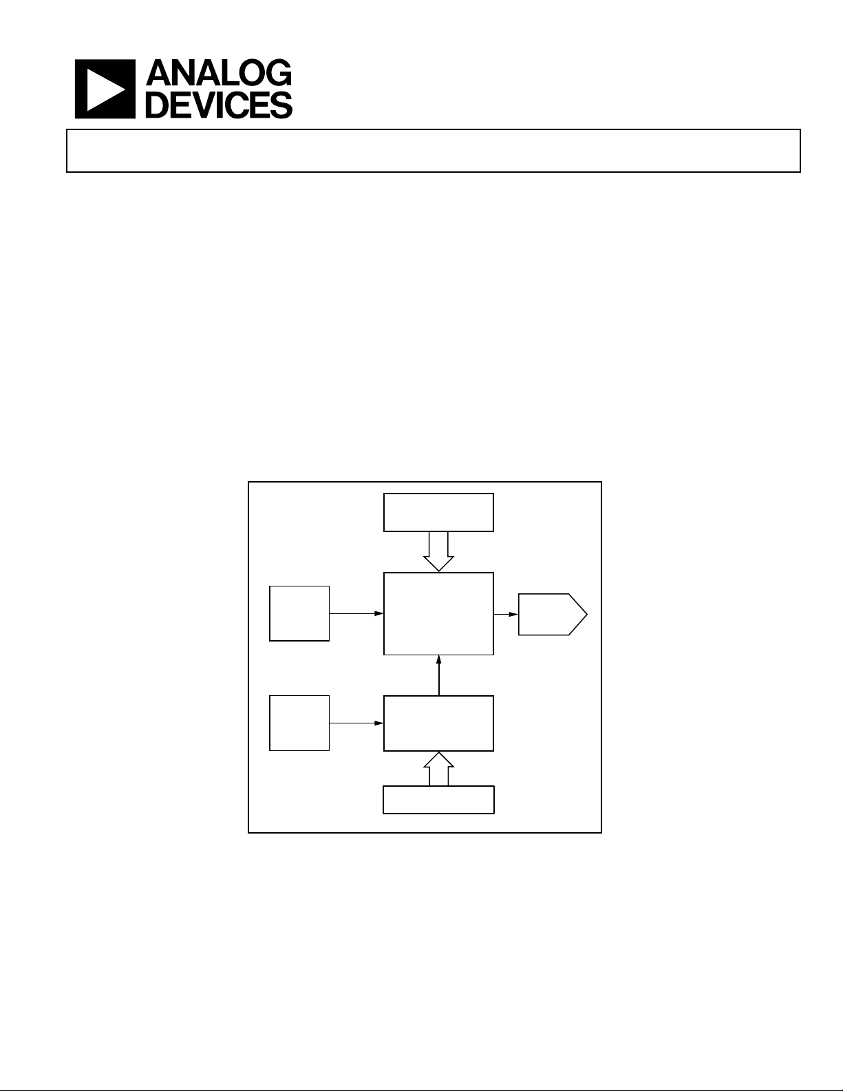
12-BIT DAC
3.5GSPS DDS CORE
TIMINGAND CONTROL
10836-001
AD9914
HIGH SPEE D P ARALLEL
MODULATION
PORT
LINEAR
SWEEP
BLOCK
SERIAL O R P ARALLEL
DATA PORT
REF CLK
MULTIPLIER
Preliminary Technical Data
FEATURES
3.5 GSPS internal clock speed
Integrated 12-bit DAC
Frequency tuning resolution to 271 pHz
16-bit phase tuning resolution
12-bit amplitude scaling
Programmable modulus
Automatic linear and nonlinear frequency sweeping
capability
32-bit parallel datapath interface
8 frequency/phase offset profiles
Phase noise −128 dBc/Hz (10 kHz offset at 1396 MHz)
Wide band SFDR <−50 dBc
Serial or parallel I/O control
1.8 V/3.3 V power supplies
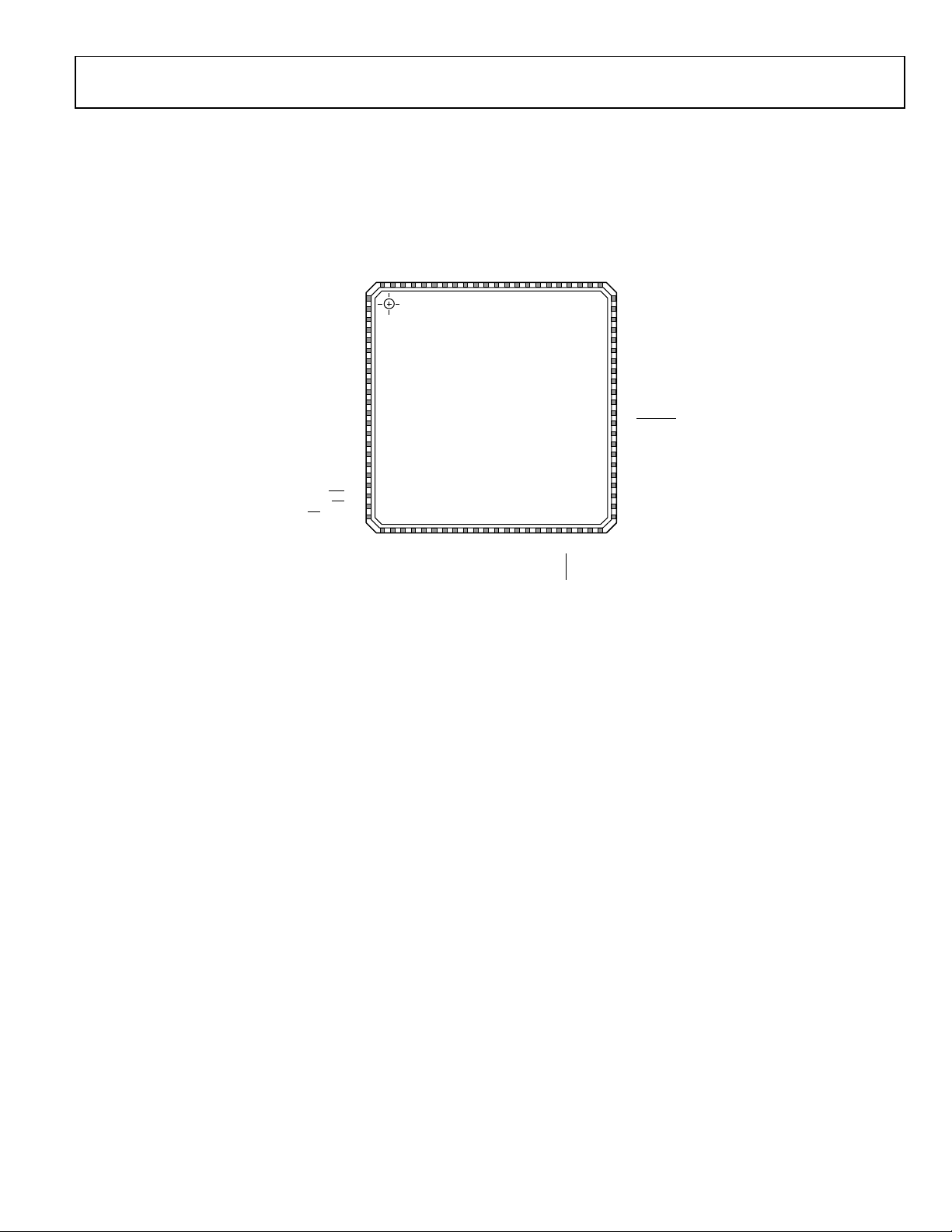
FUNCTIONAL BLOCK DIAGRAM
3.5 GSPS Direct Digital Synthesizer
Software and hardware controlled power-down
88-lead LFCSP package
PLL REF CLK multiplier
Phase modulation capability
Amplitude modulation capability
Multichip synchronization
APPLICATIONS
Agile LO frequency synthesis
Programmable clock generator
FM chirp source for radar and scanning systems
Test and measurement equipment
Acousto-optic device drivers
Polar modulator
Fast frequency hopping
responsibility is assumed by Analog Devices for its use, nor for any infringements of patents or other
rights of third parties that may result from its use. Specifications subject to change without notice. No
license is granted by implication or otherwise under any patent or patent rights of Analog Devices.
Figure 1.
One Technology Way, P.O. Box 9106, Norwood, MA 02062-9106, U.S.A.
Tel: 781.329.4700
www.analog.com
Page 2

AD9914 Preliminary Technical Data
TABLE OF CONTENTS
Features .............................................................................................. 1
Applications ....................................................................................... 1
Functional Block Diagram .............................................................. 1
General Description ......................................................................... 3
Specifications ..................................................................................... 4
DC Specifications ......................................................................... 4
AC Specifications .......................................................................... 5
Absolute Maximum Ratings ............................................................ 8
Thermal Performance .................................................................. 8
ESD Caution .................................................................................. 8
Pin Configuration and Function Descriptions ............................. 9
Typical Performance Characteristics ........................................... 12
Equivalent Circuits ......................................................................... 16
Theory of Operation ...................................................................... 17
Single Tone Mode ....................................................................... 17
Profile Modulation Mode .......................................................... 17
Digital Ramp Modulation Mode .............................................. 17
Parallel Data Port Modulation Mode ....................................... 17
Programmable Modulus Mode ................................................. 17
Functional Block Detail ................................................................. 19
DDS Core ..................................................................................... 19
12-Bit DAC Output .................................................................... 20
DAC Calibration Output ........................................................... 20
Reconstruction Filter ................................................................. 20
Clock Input (REF_CLK/
PLL Lock Indication .................................................................. 22
Output Shift Keying (OSK) ....................................................... 22
Digital Ramp Generator (DRG) ............................................... 23
Power-Down Control ................................................................ 27
Programming and Function pins ................................................. 28
Serial Programming ....................................................................... 29
Control Interface—Serial I/O ................................................... 29
General Serial I/O Operation ................................................... 29
Instruction Byte .......................................................................... 29
Serial I/O Port Pin Descriptions .............................................. 29
Serial I/O Timing Diagrams ..................................................... 30
MSB/LSB Transfers .................................................................... 30
Parallel Programming .................................................................... 31
Register Map and Bit Descriptions .............................................. 32
Outline Dimensions ....................................................................... 38
Ordering Guide .......................................................................... 38
REF_CLK
) ........................................ 21
Rev. PrJ | Page 2 of 38
Page 3
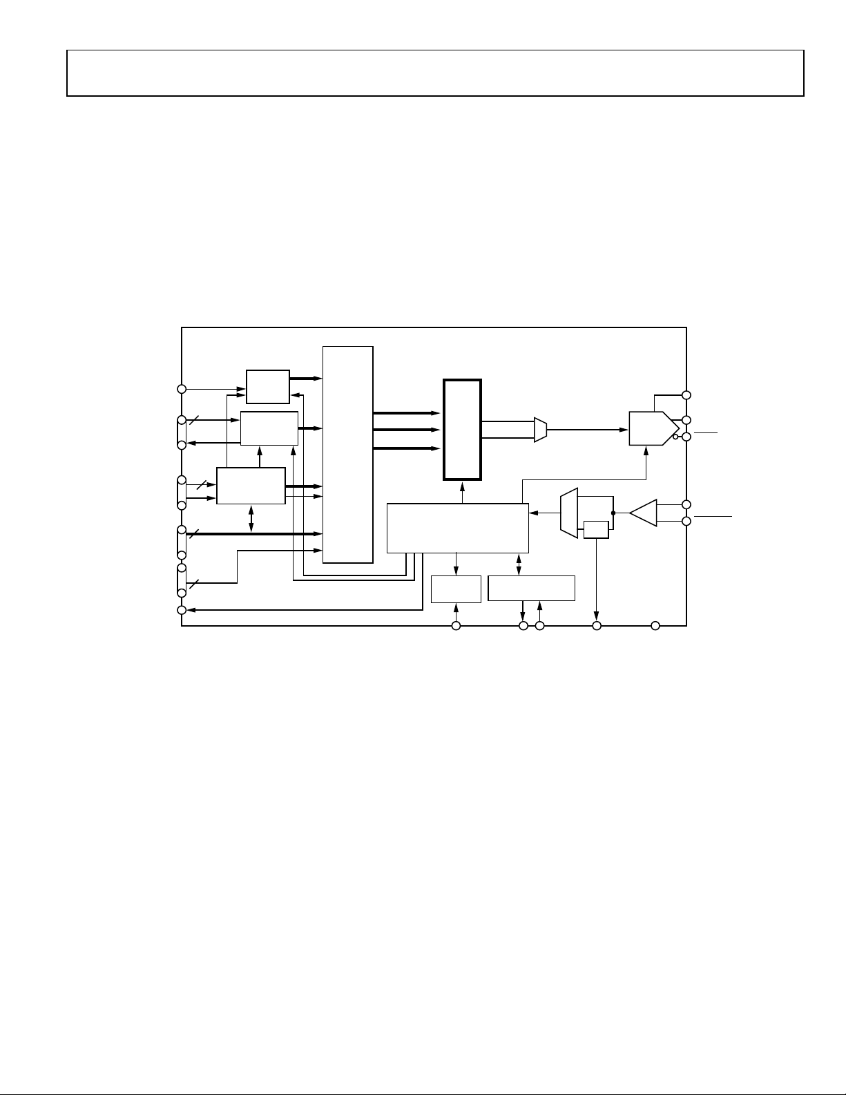
Preliminary Technical Data AD9914
10836-002
32
F0 – F3
D0 – D31
PROFILES[2:0]
I/O_UPDATE
POWER-
DOWN
CONTROL
EXT_PWR_DWN
DAC_RSET
AOUT
AOUT
OSK
DROVER
DRCTL
DRHOLD
SYNC_CLK
A
θ
CLOCK
AMPLIT UDE ( A)
FREQUENCY (ω)
PHASE (θ)
DIGITAL
RAMP
GENERATOR
2
4
MULTICHIP
SYNCHRONIZATION
SYSCLK
PLL
REF_CLK
REF_CLK
AD9914
OUTPUT
SHIFT
KEYING
DATA
ROUTE
AND
PARTITION
CONTROL
3
INTERNAL CLOCK TIMI NG
AND CONTROL
ω
Acos (ωt + θ)
Asin (ωt + θ)
SYNC_OUT
SYNC_IN
LOOP_FILTER
MASTER_RESET
DAC
12-BIT
DDS
INTERNAL
PROGRAMMING
REGISTERS
GENERAL DESCRIPTION
The AD9914 is a direct digital synthesizer (DDS) featuring a
12-bit DAC. The AD9914 uses advanced DDS technology,
coupled with an internal high speed, high performance DAC
to form a digitally programmable, complete high frequency
synthesizer capable of generating a frequency-agile analog
output sinusoidal waveform at up to 1.4 GHz. The AD9914
enables fast frequency hopping and fine tuning resolution
(64-bit capable using programmable modulus mode). The
AD9914 also offers fast phase and amplitude hopping capability.
The frequency tuning and control words are loaded into the
AD9914 via a serial or parallel I/O port. The AD9914 also
supports a user defined linear sweep mode of operation for
generating linear swept waveforms of frequency, phase, or
amplitude. A high speed, 32-bit parallel data input port is
included enabling high data rates for polar modulation schemes
and fast reprogramming of the phase, frequency, and amplitude
tuning words.
The AD9914 is specified to operate over the extended industrial
temperature range (see Absolute Maximum Ratings section).
Figure 2. Detailed Block Diagram
Rev. PrJ | Page 3 of 38
Page 4

AD9914 Preliminary Technical Data
DVDD_I/O
I
DVDD
433
mA
Pin 6, Pin 23, Pin 73
AVDD (1.8V)
Input Low Voltage (VIL)
0.8 V
INH
INL
Input Resistance
1.4 kΩ
Differential
Internally Generated DC Bias
2 V
SPECIFICATIONS
DC SPECIFICATIONS
AVDD (1.8V) and DVDD (1.8V) = 1.8 V ± 5%, AVDD (3.3V) and DVDD_I/O (3.3V) = 3.3 V ± 5%, T = 25°C, R
I
= 20 mA, external reference clock frequency = 3.5 GHz with reference clock (REF CLK) multiplier bypassed, unless otherwise noted.
OUT
Table 1.
Parameter Min Typ Max Unit Test Conditions/Comments
SUPPLY VOLTAGE
DVDD_I/O 3.135 3.30 3.465 V Pin 16, Pin 83
DVDD 1.71 1.80 1.89 V Pin 6, Pin 23, Pin 73
AVDD(3.3V) 3.135 3.30 3.465 V Pin 34, Pin 36, Pin 39, Pin 40, Pin 43, Pin 47, Pin 50, Pin 52,
Pin 53, Pin 60
AVDD (1.8V) 1.71 1.80 1.89 V Pin 32, Pin 56, Pin 57
SUPPLY CURRENT See also the total power dissipation specifications
I
20 mA Pin 16, Pin 83
I
640 mA Pin 34, Pin 36, Pin 39, Pin 40, Pin 43, Pin 47, Pin 50, Pin 52,
AVDD (3.3V)
Pin 53, Pin 60
I
178 mA Pin 32, Pin 56, Pin 57
TOTAL POWER DISSIPATION
Base DDS Power, PLL Disabled 2392 3091 mW 3.5 GHz, single-tone mode, modules disabled, linear
sweep disabled, amplitude scaler disabled
Base DDS Power, PLL Enabled 2237 2627 mW 2.5 GHz, single-tone mode, modules disabled, linear
sweep disabled, amplitude scaler disabled
Linear Sweep Additional Power 28 mW
Modulus Additional Power 20 mW
Amplitude Scaler Additional
138 mW Manual or automatic
Power
Full Power-Down Mode 400 616 mW Using either the power-down and enable register or the
EXT_PWR_DWN pin
CMOS LOGIC INPUTS
Input High Voltage (VIH) 2.0 DVDD_I/O V
= 3.3 kΩ,
SET
Input Current (I
Maximum Input Capacitance (CIN) 3 pF
CMOS LOGIC OUTPUTS
Output High Voltage (VOH) 2.7 DVDD_I/O V IOH = 1 mA
Output High Voltage (VOL) 0.4 V IOL = 1 mA
REF CLK INPUT CHARACTERISTICS REF CLK inputs should always be ac-coupled (both single-
REF CLK Multiplier Bypassed
Input Capacitance 1 pF Single-ended, each pin
Voltage
Differential Input Voltage 0.8 1.5 mV p-p
REF CLK Multiplier Enabled
Input Capacitance 1 pF Single-ended, each pin
Input Resistance 1.4 kΩ Differential
Internally Generated DC Bias
Voltage
Differential Input Voltage 0.8 1.5 mV p-p
, I
) ±60 ±200 µA At VIN = 0 V and VIN = DVDD_I/O
ended and differential)
2 V
Rev. PrJ | Page 4 of 38
Page 5

Preliminary Technical Data AD9914
AC SPECIFICATIONS
AVDD (1.8V) and DVDD (1.8V) = 1.8 V ± 5%, AVDD3 (3.3V) = 3.3 V ± 5%, DVDD_I/O (3.3V) = 3.3 V ± 5%, T = 25°C, R
I
= 20 mA, external reference clock frequency = 3.5 GHz with reference clock (REF CLK) multiplier disabled, unless otherwise noted.
OUT
Table 2.
Parameter Min Typ Max Unit Test Conditions/Comments
REF CLK INPUT Input frequency range
REF CLK Multiplier Bypassed
Input Frequency Range 500 3500 MHz Maximum f
Duty Cycle 45 55 %
Minimum Differential Input Level 632 mV p-p Equivalent to 316 mV swing on each leg
System Clock (SYSCLK) PLL Enabled
VCO Frequency Range 2400 2500 MHz
VCO Gain (KV) 50 MHz/V
Maximum PFD Rate 125 MHz
CLOCK DRIVERS
SYNC_CLK Output Driver
Frequency Range 146 MHz
Duty Cycle 45 50 55 %
Rise Time/Fall Time (20% to 80%) 650 ps
SYNC_OUT Output Driver 10 pF load
Frequency Range 9.1 MHz
Duty Cycle 33 66 % CFR2 Bit 9 = 1
Rise Time (20% to 80%) 1350 ps 10 pF load
Fall Time (20% to 80%) 1670 ps 10 pF load
DAC OUTPUT CHARACTERISTICS
Output Frequency Range (1st Nyquist
0 1750 MHz
Zone)
Output Resistance 50 Ω Single-ended (each pin internally terminated to
AVDD (3.3V))
Output Capacitance 5 pF
Full-Scale Output Current 20.48 mA Range depends on DAC R
Gain Error −10 +10 % FS
Output Offset 0.6 A
Voltage Compliance Range AVDD −
0.50
AVDD +
V
0.50
Wideband SFDR See the Typical Performance Characteristics
section
101.1 MHz Output −66 dBc 0 MHz to 1750 MHz
427.5 MHz Output −65 dBc 0 MHz to 1750 MHz
696.5 MHz Output −57 dBc 0 MHz to 1750 MHz
1396.5 MHz Output −52 dBc 0 MHz to 1750 MHz
Narrow-Band SFDR See the Typical Performance Characteristics
section
100.5 MHz Output −95 dBc ±500 kHz
427.5 MHz Output −95 dBc ±500 kHz
696.5 MHz Output −95 dBc ±500 kHz
1396.5 MHz Output −92 dBc ±500 kHz
DIGITAL TIMING SPECIFICATIONS
Time Required to Enter Power-Down TBD µs Power-down mode loses DAC/PLL calibration
settings
Time Required to Leave Power-Down TBD µs Must recalibrate DAC/PLL
Minimum Master Reset time TBD TBD
Maximum DAC Calibration Time (t
Maximum PLL Calibration Time (t
) TBD TBD f
CAL
) TBD TBD
REF_CLK
CAL
= f
Synchronization Time 16 SYNC_IN cycles
Maximum Profile Toggle Rate 1 SYNC_CLK
period
Rev. PrJ | Page 5 of 38
is 0.4 × f
OUT
/384 USR 0 register, Bit 6 = 0
SYSCLK
SYSCLK
SET
SET
resistor
= 3.3 kΩ,
Page 6
AD9914 Preliminary Technical Data
Parameter Min Typ Max Unit Test Conditions/Comments
PARALLEL PORT TIMING
Write Timing
Address Setup Time to WR Active
Address Hold Time to WR Inactive
Data Setup Time to WR Inactive
Data Hold Time to WR Inactive
WR Minimum Low Time
WR Minimum High Time
Minimum WR Time
Read Timing
Address to Data Valid 92 ns
Address Hold to RD Inactive
RD Active to Data Valid
RD Inactive to Data Tristate
RD Minimum Low Time
RD Minimum High Time
SERIAL PORT TIMING
SCLK Clock Rate (1/t
SCLK Pulse Width High, t
SCLK Pulse Width Low, t
) 80 MHz SCLK duty cycle = 50%
CLK
1.5 ns
HIGH
5.1 ns
LOW
SDIO to SCLK Setup Time, tDS 4.9 ns
SDIO to SCLK Hold Time, tDH 0 ns
SCLK Falling Edge to Valid Data on
SDIO/SDO, t
CS to SCLK Setup Time, t
CS to SCLK Hold Time, t
CS Minimum Pulse Width High, t
DV
S
H
PWH
DATA PORT TIMING
D[31:0] Setup Time to SYNC_CLK 2 ns
D[31:0] Hold Time to SYNC_CLK 0 ns
F[3:0] Setup Time to SYNC_CLK 2 ns
F[3:0] Hold Time to SYNC_CLK 0 ns
IO_UPDATE Pin Setup Time to
SYNC_CLK
IO_UPDATE Pin Hold Time to
SYNC_CLK
Profile Pin Setup Time to SYNC_CLK ns
Profile Pin Hold Time to SYNC_CLK 2 ns
DR_CTL/DR_HOLD Setup Time to
SYNC_CLK
DR_CTL/DR_HOLD Hold Time to
SYNC_CLK
DATA LATENCY (PIPELINE DELAY)
Single Tone Mode (Matched Latency
Disabled)
Frequency 320 SYSCLK cycles
Phase 296 SYSCLK cycles
Amplitude 104 SYSCLK cycles
Single Tone Mode (Matched Latency
Enabled)
Frequency 320 SYSCLK cycles
Phase 320
Amplitude 320 SYSCLK cycles
1 ns
0 ns
3.8 ns
0 ns
2.1 ns
3.8 ns
10.5 ns
0 ns
69 ns
50 ns
69 ns
50 ns
78 ns
4 ns
0 ns
4 ns
2 ns
0 ns
2 0 ns
0 ns
SYSCLK cycles = fS = system clock frequency
in GHz
Rev. PrJ | Page 6 of 38
Page 7

Preliminary Technical Data AD9914
Parameter Min Typ Max Unit Test Conditions/Comments
Profile Pin Selection Mode
Frequency 320 SYSCLK cycles
Phase 296 SYSCLK cycles
Amplitude 104 SYSCLK cycles
Modulation Mode with 32-Bit Parallel
Port
Frequency 296 SYSCLK cycles
Phase 272 SYSCLK cycles
Amplitude 80 SYSCLK cycles
Sweep Mode
Frequency 392 SYSCLK cycles
Phase 368 SYSCLK cycles
Amplitude 176 SYSCLK cycles
Rev. PrJ | Page 7 of 38
Page 8
AD9914 Preliminary Technical Data
per JEDEC JESD51-6
θ
Junction-to-board thermal
13.3
°C/W
ABSOLUTE MAXIMUM RATINGS
Table 3.
Parameter Rating
AVDD (1.8V), DVDD (1.8V) Supplies 2 V
AVDD (3.3V), DVDD_I/O (3.3V) Supplies 4 V
Digital Input Voltage −0.7 V to +4 V
Digital Output Current 5 mA
Storage Temperature Range −65°C to +150°C
Operating Temperature Range −40°C to +85°C
Maximum Junction Temperature 150°C
Lead Temperature (10 sec Soldering) 300°C
Stresses above those listed under Absolute Maximum Ratings
may cause permanent damage to the device. This is a stress
rating only; functional operation of the device at these or any
other conditions above those indicated in the operational
section of this specification is not implied. Exposure to absolute
maximum rating conditions for extended periods may affect
device reliability.
THERMAL PERFORMANCE
Table 4.
Symbol Description Value1 Unit
θJA
θ
JMA
θ
JMA
JB
ΨJB
θJC
ΨJT
1
Results are from simulations. PCB is JEDEC multilayer. Thermal performance
for actual applications requires careful inspection of the conditions in the
application to determine if they are similar to those assumed in these
calculations.
Junction-to-ambient thermal
resistance (Still Air) per JEDEC
JESD51-2
Junction-to-ambient thermal
resistance (1.0 m/sec airflow)
per JEDEC JESD51-6
Junction-to-ambient thermal
resistance (2.0 m/sec air flow)
resistance (still air) per JEDEC
JESD51-8
Junction-to-board characterization
parameter (still air) per JEDEC
JESD51-6
Junction-to-case thermal resistance 2.21 °C/W
Junction-to-top-of-package
characterization parameter (still air)
per JEDEC JESD51-2
24.1 °C/W
21.3 °C/W
20.0 °C/W
12.8 °C/W
0.23 °C/W
ESD CAUTION
Rev. PrJ | Page 8 of 38
Page 9
Preliminary Technical Data AD9914
1
2
3
4
5
6
7
8
9
10
11
12
13
14
15
16
D17
D16
D15/A7
D14/A6
D13/A5
DVDD (1.8V)
DGND
D12/A4
D11/A3
D10/A2
D9/A1
D8/A0
D7
D6
D5
DVDD_I/O ( 3.3V)
17DGND
18D4/SYNCIO
19D3/SDO
20D2/SDIO/WR
23242526272829303132333436
37
DVDD (1.8V)
DGND
PS0
PS1
PS2
F0F1F2
F3
AVDD (1.8V)
AGND
AVDD (3.3V)
35AGND
AVDD (3.3V)
AGND
38AGND
39AVDD (3.3V)
40AVDD (3.3V)
41
AOUT
58
57
56
55
54
53
52
51
50
49
48
47
46
45
LOOP_FILTER
59 REF
60 AVDD (3.3V)
61 SYNC_OUT
62 SYNC_IN
63 DRCTL
64 DRHOLD
65 DROVER
66 OSK
AVDD (1.8V)
AVDD (1.8V)
REF CLK
REF CLK
AVDD (3.3V)
AVDD (3.3V)
AGND
AVDD (3.3V)
AGND
DAC_RSET
AVDD (3.3V)
AGND
DAC_BP
7877767574737271706968
67
D23
79 D22
80 D21
81 D20
82 SYNC_CLK
83 DVDD_I/O ( 3.3V)
84 DGND
85 MASTER_RESET
86 I/O_UPDATE
87 D19
88 D18
D24
D25
D26
DGND
DVDD (1.8V)
D27
D28
D29
D30
D31
EXT_PWR_DWN
NOTES
1. THE EPAD M US T BE SOLDERED TO GROUND.
10836-003
21D1/SCLK/RD
22D0/CS/PWD
42AOUT
43AVDD (3.3V)
44AGND
AD9914
TOP VIEW
(Not to S cale)
PIN CONFIGURATION AND FUNCTION DESCRIPTIONS
Figure 3. Pin Configuration
Rev. PrJ | Page 9 of 38
Page 10
AD9914 Preliminary Technical Data
Table 5. Pin Function Descriptions
Pin No. Mnemonic I/O1 Description
1, 2, 13 to 15, 68
to 72, 75 to 81,
87, 88
3 D15/A7 I/O Parallel Port Pin/Address Line. Multipurpose pin depending on the state of the function pins
4 D14/A6 I/O Parallel Port Pin/Address Line. Multipurpose pin depending on the state of the function pins
5 D13/A5 I/O Parallel Port Pin/Address Line. Multipurpose pin depending on the state of the function pins
8 D12/A4 I/O Parallel Port Pin/Address Line. Multipurpose pin depending on the state of the function pins
9 D11/A3 I/O Parallel Port Pin/Address Line. The state of the F0 to F3 function pins determines if this acts as
10 D10/A2 I/O Parallel Port Pin/Address Line. Multipurpose pin depending on the state of the function pins
11 D9/A1 I/O Parallel Port Pin/Address Line. Multipurpose pin depending on the state of the function pins
12 D8/A0 I/O Parallel Port Pin/Address Line. Multipurpose pin depending on the state of the function pins
18 D4/SYNCIO I Parallel Port Pin/Serial Port Synchronization Pin. Multipurpose pin depending on the state of
19 D3/SDO I/O Parallel Port Pin/Serial Data Output. Multipurpose pin depending on the state of the function
20 D2/SDIO/WR I/O Parallel Port Pin/Serial Data Input and Output/Write Input. Multipurpose pin depending on
21 D1/SCLK/RD I Parallel Port Pin/Serial Clock/Read Input. Multipurpose pin depending on the state of the
22 D0/CS/PWD I Parallel Port Pin/Chip Select/Parallel Width. Multipurpose pin depending on the state of the
6, 23, 73 DVDD (1.8V) I Digital Core Supplies (1.8 V).
7, 17, 24, 74, 84 DGND I Digital Ground.
16, 83 DVDD_I/O (3.3V) I Digital Input/Output Supplies (3.3 V).
32, 56, 57 AVDD (1.8V) I Analog Core Supplies (1.8 V).
33, 35, 37, 38,
44, 46, 49, 51
34, 36, 39, 40,
43, 47, 50, 52,
53, 60
D5 to D7, D16 to
D31, D27 to D31
AGND I Analog Ground.
AVDD (3.3V) I Analog DAC Supplies (3.3 V).
I/O Parallel Port Pins. The 32-bit parallel port offers the option for serial or parallel programming
of the internal registers. In addition, the parallel port can be configured to provide direct FSK,
PSK, or ASK (or combinations thereof ) modulation data. The 32-bit parallel port configuration
is set by the state of the four function pins (F0 to F3).
(F0 to F3). The state of the F0 to F3 function pins determines if this acts as a line for direct
FSK, PSK, or ASK data or as an address line for programming the internal registers.
(F0 to F3). The state of the F0 to F3 function pins determines if this acts as a line for direct
FSK, PSK, or ASK data or as an address line for programming the internal registers.
(F0 to F3). The state of the F0 to F3 function pins determines if this acts as a line for direct
FSK, PSK, or ASK data or as an address line for programming the internal registers.
(F0 to F3). The state of the F0 to F3 function pins determines if this acts as a line for direct
FSK, PSK, or ASK data or as an address line for programming the internal registers.
a line for direct FSK, PSK, or ASK data or as an address line for programming the internal
registers.
(F0 to F3). The state of the F0 to F3 function pins determines if this acts as a line for direct
FSK, PSK, or ASK data or as an address line for programming the internal registers.
(F0 to F3). The state of the F0 to F3 function pins determines if this acts as a line for direct
FSK, PSK, or ASK data or as an address line for programming the internal registers.
(F0 to F3). The state of the F0 to F3 function pins determines if this acts as a line for direct
FSK, PSK, or ASK data or as an address line for programming the internal registers.
the function pins (F0 to F3). This pin is D4 for direct FSK, PSK, or ASK data. If serial mode is
invoked via F0 to F3, this pin is used to reset the serial port.
pins (F0 to F3). This pin is D3 for direct FSK, PSK, or ASK data. If serial mode is invoked via (F0F3), this pin is used for readback mode for serial operation.
the state of the function pins (F0 to F3). This pin is D2 for direct FSK, PSK, or ASK data. If serial
mode is invoked via F0 to F3, this pin is used for the SDIO for serial operation. If parallel mode
is enabled, this pin is used to write to change the values of the internal registers.
function pins (F0 to F3). This pin is D1 for direct FSK, PSK, or ASK data. If serial mode is
invoked via F0 to F3, this pin is used for SCLK for serial operation. If parallel mode is enabled,
this pin is used to read back the value of the internal registers.
function pins (F0 to F3). This pin is D0 for direct FSK, PSK, or ASK data. If serial mode is
invoked via F0 to F3, this pin is used for the chip select for serial operation. If parallel mode is
enabled, this pin is used to set either 8-bit data or 16-bit data.
Rev. PrJ | Page 10 of 38
Page 11

Preliminary Technical Data AD9914
up on the SYNC_CLK pin.
28, 29, 30, 31
F0 to F3
I
Function Pins. Digital Inputs. The state of these pins determine if a serial or parallel interface
63
DRCTL
I
Ramp Control. Digital input (active high). This pin controls the sweep direction (up/down).
64
DRHOLD
I
Ramp Hold. Digital input (active high). Pauses the sweep when active.
Pin No. Mnemonic I/O1 Description
25, 26, 27 PROFILE[0:2] I Profile Select Pins. Digital inputs (active high). Use these pins to select one of eight
phase/frequency profiles for the DDS. Changing the state of one of these pins transfers the
current contents of all I/O buffers to the corresponding registers. State changes should be set
is used. In addition, the function pins determine how the 32-bit parallel data-word is
partitioned for FSK, PSK, or ASK modulation mode.
41
42 AOUT O DAC Output Source. Analog output (voltage mode). Internally connected through a 50 Ω
45 DAC_BP I DAC Bypass Pin.
48 DAC_RSET O Analog Reference. This pin programs the DAC output full-scale reference current. Connect a
54
55 REF_CLK I Reference Clock Input. Analog input.
58 LOOP_FILTER O External PLL Loop Filter Node.
59 REF O Local PLL Reference Supply. Typically at 2.05 V.
61 SYNC_OUT O Digital Synchronization Output. Used to synchronize multiple chips together.
62 SYNC_IN I Digital Synchronization Input. Used to synchronize multiple chips together.
O DAC Complementary Output Source. Analog output (voltage mode). Internally connected
AOUT
through a 50 Ω resistor to AVDD (3.3V).
resistor to AVDD (3.3V).
3.3 kΩ resistor to AGND.
REF_CLK
I Complementary Reference Clock Input. Analog input.
65 DROVER O Ramp Over. Digital output (active high). This pin switches to Logic 1 whenever the digital
ramp generator reaches its programmed upper or lower limit.
66 OSK I Output Shift Keying. Digital input (active high). When the OSK features are placed in either
manual or automatic mode, this pin controls the OSK function. In manual mode, it toggles
the multiplier between 0 (low) and the programmed amplitude scale factor (high). In
automatic mode, a low sweeps the amplitude down to zero and a high sweeps the
amplitude up to the amplitude scale factor.
67 EXT_PWR_DWN I External Power-Down. Digital input (active high). A high level on this pin initiates the
currently programmed power-down mode.
82 SYNC_CLK O Clock Output. Digital output. Many of the digital inputs on the chip, such as I/O_UPDATE,
PROFILE[2:0], and the parallel data port (D0 to D31), must be set up on the rising edge of this
signal.
85 MASTER_RESET I Master Reset. Digital input (active high). Clears all memory elements and sets registers to
default values.
86 I/O_UPDATE I Input/Output Update. Digital input (active high). A high on this pin transfers the contents of
the I/O buffers to the corresponding internal registers.
EPAD Exposed Pad. The EPAD must be soldered to ground.
1
I = input, O = output.
Rev. PrJ | Page 11 of 38
Page 12
AD9914 Preliminary Technical Data
START 0Hz
–100
–90
–80
–70
–60
–50
–40
–30
–20
–10
0
175MHz/DIV STOP 1.75GHz
SFDR (dBc)
10836-004
START 0Hz
–100
–90
–80
–70
–60
–50
–40
–30
–20
–10
0
175MHz/DIV STOP 1.75GHz
SFDR (dBc)
10836-005
START 0Hz
–100
–90
–80
–70
–60
–50
–40
–30
–20
–10
0
175MHz/DIV STOP 1.75GHz
SFDR (dBc)
10836-006
CENTER 171.5MHz
–100
–90
–80
–70
–60
–50
–40
–30
–20
–10
0
50kHz/DIV SPAN 500kHz
SFDR (dBc)
10836-007
CENTER 427.5MHz
–100
–90
–80
–70
–60
–50
–40
–30
–20
–10
0
50kHz/DIV SPAN 500kHz
SFDR (dBc)
10836-008
CENTER 696.5MHz
–100
–90
–80
–70
–60
–50
–40
–30
–20
–10
0
50kHz/DIV SPAN 500kHz
SFDR (dBc)
10836-009
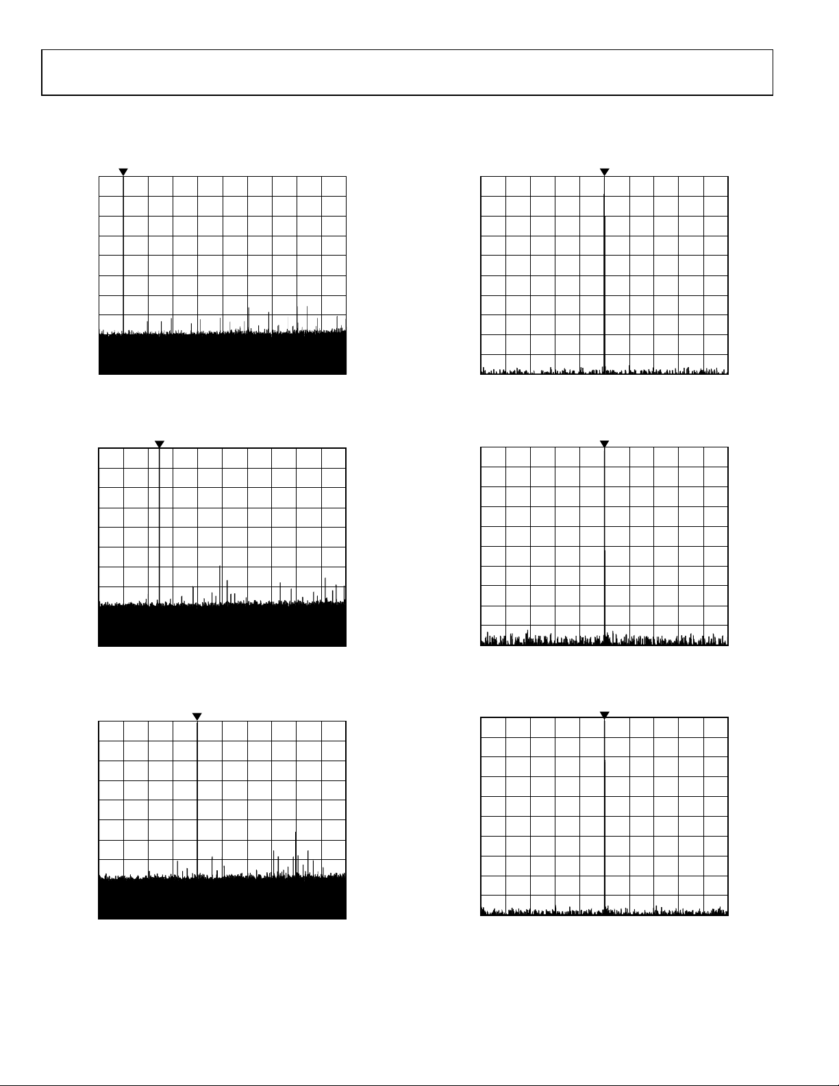
TYPICAL PERFORMANCE CHARACTERISTICS
Nominal supply voltage; DAC R
= 3.3 kΩ, 25°C, unless otherwise noted.
SET
Figure 4. Wideband SFDR at 171.5 MHz
SYSCLK = 3.5 GHz (SYSCLK PLL Bypassed)
Figure 5. Wideband SFDR at 427.5 MHz
SYSCLK = 3.5 GHz (SYSCLK PLL Bypassed)
Figure 7. Narrow-Band SFDR at 171.5 MHz,
SYSCLK = 3.5 GHz (SYSCLK PLL Bypassed)
Figure 8. Narrow-Band SFDR at 427.5 MHz,
SYSCLK = 3.5 GHz (SYSCLK PLL Bypassed)
Figure 6. Wideband SFDR at 696.5 MHz,
SYSCLK = 3.5 GHz (SYSCLK PLL Bypassed)
Rev. PrJ | Page 12 of 38
Figure 9. Narrow-Band SFDR at 696.5 MHz,
SYSCLK = 3.5 GHz (SYSCLK PLL Bypassed)
Page 13

Preliminary Technical Data AD9914
–100
–90
–80
–70
–60
–50
–40
–30
–20
–10
0
SFDR (dBc)
START 0Hz 175MHz/DIV STOP 1.75GHz
10836-010
0
–80
0 0.05 0.10 0.15 0.400.350.300.250.20
SFDR (dBc)
f
C
/
f
S
–70
–60
–50
–40
–30
–20
–10
10836-011
0
–80
0 0.05 0.10 0.15 0.400.350.300.250.20
SFDR (dBc)
f
C
/
f
S
–70
–60
–50
–40
–30
–20
–10
10836-012
SYSCLK = 2. 7GHz
SYSCLK = 2. 8GHz
SYSCLK = 2. 9GHz
SYSCLK = 3. 0GHz
SYSCLK = 3. 1GHz
SYSCLK = 3. 2GHz
SYSCLK = 3. 3GHz
SYSCLK = 3. 4GHz
SYSCLK = 3. 5GHz
SYSCLK = 1. 5GHz
SYSCLK = 1. 6GHz
SYSCLK = 1. 7GHz
SYSCLK = 1. 8GHz
SYSCLK = 1. 9GHz
SYSCLK = 2. 0GHz
SYSCLK = 2. 1GHz
SYSCLK = 2. 2GHz
SYSCLK = 2. 3GHz
SYSCLK = 2. 4GHz
SYSCLK = 2. 5GHz
SYSCLK = 2. 6GHz
CENTER 1.3965MHz
–100
–90
–80
–70
–60
–50
–40
–30
–20
–10
0
50kHz/DIV SPAN 500kHz
SFDR (dBc)
10836-013
10 100 1k 10k 100k 1M 10M 100M
FREQUENCY OFFSET (Hz)
–70
–90
–80
–100
–110
–120
–130
–140
–150
–160
–170
PHASE NOISE (dBc/Hz)
SMA
SMA AND
ADCLK925
10836-014
10 100 1k 10k 100k 1M 10M 100M
FREQUENCY OFFSET (Hz)
–70
–90
–80
–100
–110
–120
–130
–140
–150
–160
–170
PHASE NOISE (dBc/Hz)
1396MHz
696MHz
427MHz
171MHz
10836-015
Figure 10. Wideband SFDR at 1396.5 MHz,
SYSCLK = 3.5 GHz (SYSCLK PLL Bypassed)
Figure 11. Wideband SFDR vs. Normalized f
SYSCLK = 3.5 GHz
OUT
Figure 13. Narrow-Band SFDR at 1396.5 MHz,
SYSCLK = 3.5 GHz (SYSCLK PLL B ypassed)
Figure 14. Absolute Phase Noise of REF CLK Source Driving AD9914
Rohde & Schwarz SMA100 Signal Generator at 3.5 GHz Buffered by Series
ADCLK925
Figure 12. Wideband SFDR vs. Normalized f
SYSCLK = 2.5 GHz to 3.5 GHz
OUT
,
Figure 15. Absolute Phase Noise Curves of DDS Output at 3.5 GHz Operation
Rev. PrJ | Page 13 of 38
Page 14

AD9914 Preliminary Technical Data
10 1k 100k 10M
FREQUENCY OFFSET (Hz)
–70
–90
–80
–100
–110
–120
–130
–140
–150
–160
–170
PHASE NOISE (dBc/Hz)
1396MHz
NORMALIZED
REF CLK SO URCE
10836-016
10 1k 100k 10M
FREQUENCY OFFSET (Hz)
–60
–90
–80
–70
–100
–110
–120
–130
–140
–150
–160
–170
–180
PHASE NOISE (dBc/Hz)
1396MHz
696MHz
427MHz
171MHz
10836-017
0.5
0.4
0.3
0.2
0.1
0
500 1000 400035003000250020001500
SUPPLY CURRENT (A)
SYSTEM CLOCK (MHz)
10836-018
3.3V ANALOG
3.3V DIGITAL
1.8V ANALOG
1.8V DIGITAL
10
FREQUENCY OFFSET (Hz)
–70
–90
–80
–100
–110
–120
–130
–140
–150
–160
–170
PHASE NOISE (dBc/Hz)
978MHz
305MHz
123MHz
1k 100k 10M
497MHz
10836-019
10 1k 100k 10M
FREQUENCY OFFSET (Hz)
–60
–90
–80
–70
–100
–110
–120
–130
–140
–150
–160
PHASE NOISE (dBc/Hz)
1396MHz ABSOLUTE
1396MHz RESIDUAL
10836-020
–60
–90
–80
–70
–100
–110
–120
–130
–140
–150
–160
–170
–180
10 1k 100k 10M
FREQUENCY OFFSET (Hz)
PHASE NOISE (dBc/Hz)
1396MHz ABSOLUTE
1396MHz RESIDUAL
10836-021
Figure 16. Absolute Phase Noise Curves of Normalized REF CLK Source to
DDS Output at 1396 MHz (SYSCLK = 3.5 GHz)
Figure 17. Residual Phase Noise Curves
Figure 19. Absolute Phase Noise Curves of DDS Output Using Internal PLL at
2.5 GHz Operation
Figure 20. Residual PN vs. Absolute PN Measurement Curves at 1396 MHz
Figure 18. Power Supply Current vs. SYSCLK
Figure 21. Residual Phase Noise
Rev. PrJ | Page 14 of 38
Page 15

Preliminary Technical Data AD9914
10836-022
CH2 1.0V Ω M20.00ms IT 40.0ps/pt
A CH2 1.64V
1
10
9
1
2
3
4
5
6
7
8
0
100 4100
TIME (ms)
SYSTEM CLOCK RATE (MHz)
600 1100 1600 2100 2600 3100 3600
10836-023
930
870
880
890
900
910
920
–6 –2–4 6420
FREQUENCY ( Hz )
TIME (ms)
10836-024
930
870
880
890
900
910
920
–6 –2–4 6420
FREQUENCY ( Hz )
TIME (ms)
10836-025
Figure 22. SYNC_OUT (SYSCLK/384)
Figure 24. Measured Rising Linear Frequency Sweep
Figure 23. DAC Calibration Time vs. SYSCLK Rate
Figure 25. Measured Falling Linear Frequency Sweep
Rev. PrJ | Page 15 of 38
Page 16

AD9914 Preliminary Technical Data
10836-044
SWITCH
CONTROL
CODE
IFS/2 IFS/2
AVDD (3.3V)
AGND
CURRENT
SWITCH
ARRAY
CURRENT
SWITCH
ARRAY
AOUT
AOUT
INTERNAL
50Ω
INTERNAL
50Ω
IFS/2 + I
CODE
I
FS
/2 – I
CODE
I
FS
41
42
TBD
TBD
DVDD (3.3V)
10836-043
EQUIVALENT CIRCUITS
Figure 26. DAC Output
Figure 28. CMOS Input
Figure 27. REF CLK input
Figure 29. CMOS Output
Rev. PrJ | Page 16 of 38
Page 17

Preliminary Technical Data AD9914
THEORY OF OPERATION
The AD9914 has five modes of operation.
• Single tone
• Profile modulation
• Digital ramp modulation (linear sweep)
• Parallel data port modulation
• Programmable modulus mode
The modes define the data source used to supply the DDS with
its signal control parameters: frequency, phase, or amplitude.
The partitioning of the data into different combinations
of frequency, phase, and amplitude is established based on the
mode and/or specific control bits and function pins.
Although the various modes are described independently, they
can be enabled simultaneously. This provides an unprecedented
level of flexibility for generating complex modulation schemes.
However, to avoid multiple data sources from driving the same
DDS signal control parameter, the device has a built-in priority
protocol.
In single tone mode, the DDS signal control parameters come
directly from the profile programming registers. In digital ramp
modulation mode, the DDS signal control parameters are
delivered by a digital ramp generator. In parallel data port
modulation mode, the DDS signal control parameters are driven
directly into the parallel port.
The various modulation modes generally operate on only one of
the DDS signal control parameters (two in the case of the polar
modulation format via the parallel data port). The unmodulated
DDS signal control parameters are stored in programming
registers and automatically routed to the DDS based on the
selected mode.
A separate output shift keying (OSK) function is also available.
This function employs a separate digital linear ramp generator
that only affects the amplitude parameter of the DDS. The OSK
function has priority over the other data sources that can drive
the DDS amplitude parameter. As such, no other data source
can drive the DDS amplitude when the OSK function is enabled.
SINGLE TONE MODE
In single tone mode, the DDS signal control parameters are
supplied directly from the profile programming registers. A
profile is an independent register that contains the DDS signal
control parameters. Eight profile registers are available. Note
that the profile pins must be used to select the desired register.
PROFILE MODULATION MODE
Each profile is independently accessible. For FSK, PSK, or ASK
modulation, use the three external profile pins (PROFILE[2:0])
to select the desired profile. A change in the state of the profile
pins with the next rising edge on SYNC_CLK updates the DDS
with the parameters specified by the selected profile. Therefore,
the profile change must meet the setup and hold times to the
SYNC_CLK rising edge. Note that amplitude control must also
Rev. PrJ | Page 17 of 38
be enabled using the OSK enable bit in Register
CFR1(0x000[8]).
DIGITAL RAMP MODULATION MODE
In digital ramp modulation mode, the modulated DDS signal
control parameter is supplied directly from the digital ramp
generator (DRG). The ramp generation parameters are
controlled through the serial or parallel I/O port.
The ramp generation parameters allow the user to control both
the rising and falling slopes of the ramp. The upper and lower
boundaries of the ramp, the step size and step rate of the rising
portion of the ramp, and the step size and step rate of the falling
portion of the ramp are all programmable.
The ramp is digitally generated with 32-bit output resolution.
The 32-bit output of the DRG can be programmed to affect
frequency, phase, or amplitude. When programmed for frequency,
all 32 bits are used. However, when programmed for phase or
amplitude, only the 16 MSBs or 12 MSBs, respectively, are used.
The ramp direction (rising or falling) is externally controlled by
the DRCTL pin. An additional pin (DRHOLD) allows the user
to suspend the ramp generator in its present state. Note that
amplitude control must also be enabled using the OSK enable
bit in Register CFR1.
PARALLEL DATA PORT MODULATION MODE
In parallel data port modulation mode, the modulated DDS
signal control parameter(s) are supplied directly from the 32-bit
parallel data port. The function pins define how the 32-bit dataword is applied to the DDS signal control parameters. Formatting of the 32-bit data-word is unsigned binary, regardless of the
destination.
Parallel Data Clock (SYNC_CLK)
The AD9914 generates a clock signal on the SYNC_CLK pin
that runs at 1/24 of the DAC sample rate (the sample rate of the
parallel data port). SYNC_CLK serves as a data clock for the
parallel port.
PROGRAMMABLE MODULUS MODE
In programmable modulus mode, the DRG is used as an
auxiliary accumulator to alter the frequency equation of the
DDS core, making it possible to implement fractions that are
not restricted to a power of 2 in the denominator. A standard
DDS is restricted to powers of 2 as a denominator because the
phase accumulator is a set of bits as wide as the frequency
tuning word (FTW).
When in programmable modulus mode, however, the
frequency equation is:
f
= (fS)(FTW + A/B)/232
0
where f
This equation implies a modulus of B × 2
the case of a standard DDS). Furthermore, because B is
< ½, 0 ≤ FTW < 2
0/fS
31
, 2 ≤ B ≤ 232 – 1, and A < B.
32
(rather than 232, in
Page 18

AD9914 Preliminary Technical Data
programmable, the result is a DDS with a programmable
modulus.
When in programmable modulus mode, the 32-bit auxiliary
accumulator operates in a way that allows it to roll over at a
value other than its full capacity of 2
32
. That is, it operates with a
modified modulus based on the programmable value of B. With
each roll over of the auxiliary accumulator, a value of 1 LSB
adds to the current accumulated value of the 32-bit phase
accumulator. This behavior changes the modulus of the phase
accumulator to B × 2
the desired f
.
0
32
(instead of 232) allowing it to synthesize
To determine the programmable modulus mode register values
for FTW, A, and B the user must first define f
relatively prime integers, M/N. That is, having converted f
f
to integers, M and N, reduce the fraction, M/N, to lowest
S
terms. Then, divide M × 2
32
by N. The integer part of this
as a ratio of
0/fS
and
0
division operation is the value of FTW (Register 0x04[31:0]).
The remainder, Y, of this division operation is
32
Y = (2
×M) – (FTW×N)
The value of Y facilitates the determination of A and B by
taking the fraction, Y/N, and reducing it to lowest terms. Then,
the numerator of the reduced fraction is A (Register 0x06[31:0])
and the denominator is the B (Register 0x05[31:0]).
For example, synthesizing precisely 300 MHz with a 1 GHz
system clock is not possible with a standard DDS. It is possible,
however, using programmable modulus as follows.
First, express f
as a ratio of integers:
0/fS
300,000,000/1,000,000,000
Reducing this fraction to lowest terms yields 3/10; therefore, M
= 3 and N = 10. FTW is the integer part of (M × 2
32
2
)/10, which is 1,288,490,188 (0x4CCCCCCC in 32-bit
hexadecimal notation). The remainder, Y, of (3 × 2
32
)/N, or (3 ×
32
)/10, is (232
× 3) − (1,288,490,188 × 10), which is 8. Therefore, Y/N is 8/10,
which reduces to 4/5. Therefore, A = 4 and B = 5 (0x00000004
and 0x00000005 in 32-bit hexadecimal notation, respectively).
Programming the AD9914 with these values of FTW, A, and B
results in an output frequency that is exactly 3/10 of the system
clock frequency.
Rev. PrJ | Page 18 of 38
Page 19

Preliminary Technical Data AD9914
SYSCLK
OUT
f
FTW
f
=
32
2
=
SYSCLK
OUT
f
f
FTW
32
2round
SYSCLK
OUT
f
FTW
f
−=
32
2
1
=∆
14
14
2
360
2
2
POW
POW
π
θ
=
12
12
2
log20
2
ASF
ASF
ScaleAmplitude
DDS_CLK
32 17
FREQUENCY
CONTROL
ANGLE-TOAMPLITUDE
CONVERSION
(SINE OR
COSINE)
PHASE
OFFSET
CONTROL
TO DAC
(MSBs)
D Q
R
ACCUMULATOR
RESET
32
14
MSB ALIGNED
AMPLITUDE
CONTROL
12
DDS SIGNAL CONTROL PARAMETERS
14
12
17
32
32
12
12
32-BIT
ACCUMULATOR
10836-026
FUNCTIONAL BLOCK DETAIL
DDS CORE
The direct digital synthesizer (DDS) block generates a reference
signal (sine or cosine based on CFR1[16], the enable sine output
bit). The parameters of the reference signal (frequency, phase,
and amplitude) are applied to the DDS at its frequency, phase
offset, and amplitude control inputs, as shown in Figure 30.
The output frequency (f
) of the AD9914 is controlled by the
OUT
frequency tuning word (FTW) at the frequency control input to
the DDS. The relationship among f
, FTW, and f
OUT
SYSCLK
is given by
(1)
where FTW is a 32-bit integer ranging in value from 0 to
2,147,483,647 (2
31
− 1), which represents the lower half of the
full 32-bit range. This range constitutes frequencies from dc to
Nyquist (that is, ½ f
The FTW required to generate a desired value of f
SYSCLK
).
is found
OUT
by solving Equation 1 for FTW, as given in Equation 2.
where the upper quantity is for the phase offset expressed as
radian units and the lower quantity as degrees.
To find the POW value necessary to develop an arbitrary Δθ,
solve the preceding equation for POW and round the result (in
a manner similar to that described previously for finding an
arbitrary FTW).
The relative amplitude of the DDS signal can be digitally scaled
(relative to full scale) by means of a 12-bit amplitude scale
factor (ASF). The amplitude scale value is applied at the output
of the angle-to-amplitude conversion block internal to the DDS
core. The amplitude scale is given by
(3)
(2)
where the round(x) function rounds the argument (the value of
x) to the nearest integer. This is required because the FTW is
constrained to be an integer value. For example, for f
41 MHz and f
= 122.88 MHz, FTW = 1,433,053,867
SYSCLK
OUT
=
(0x556AAAAB).
Programming an FTW greater than 2
31
produces an aliased
image that appears at a frequency given by
(for FTW ≥ 231)
The relative phase of the DDS signal can be digitally controlled
by means of a 16-bit phase offset word (POW). The phase offset
is applied prior to the angle-to-amplitude conversion block
internal to the DDS core. The relative phase offset (Δθ) is given by
where the upper quantity is amplitude expressed as a fraction of
full scale and the lower quantity is expressed in decibels relative
to full scale.
To find the ASF value necessary for a particular scale factor, solve
Equation 3 for ASF and round the result (in a manner similar
to that described previously for finding an arbitrary FTW).
When the AD9914 is programmed to modulate any of the DDS
signal control parameters, the maximum modulation sample
rate is ¼ f
images at multiples of ¼ f
. This means that the modulation signal exhibits
SYSCLK
. The impact of these images
SYSCLK
must be considered when using the device as a modulator.
Figure 30. DDS Block Diagram
Rev. PrJ | Page 19 of 38
Page 20

AD9914 Preliminary Technical Data
PRIMARY
SIGNAL
FILTER
RESPONSE
SIN(x)/x
ENVELOPE
SPURS
IMAGE 0 IMAGE 1 I MAGE 2 IMAGE 3 IMAGE 4
0
–20
–40
–60
–80
–100
MAGNITUDE
(dB)
f
s
/2
f
s
3
f
s
/2 2
f
s
5
f
s
/2
f
BASE BAND
10836-027
12-BIT DAC OUTPUT
The AD9914 incorporates an integrated 12-bit, current output
DAC. The output current is delivered as a balanced signal using
two outputs. The use of balanced outputs reduces the potential
amount of common-mode noise present at the DAC output,
offering the advantage of an increased signal-to-noise ratio. An
external resistor (R
) connected between the DAC_RSET pin
SET
and AGND establishes the reference current. The recommended
value of R
is 3.3 kΩ.
SET
Attention should be paid to the load termination to keep the
output voltage within the specified compliance range; voltages
developed beyond this range cause excessive distortion and can
damage the DAC output circuitry.
DAC CALIBRATION OUTPUT
The DAC CAL enable bit in the DAC control register (0x03[24])
must be manually set and then cleared after each power-up and
every time the REF CLK or internal system clock is changed.
This initiates an internal calibration routine to optimize the
setup and hold times for internal DAC timing. Failure to
calibrate degrades ac performance.
RECONSTRUCTION FILTER
The DAC output signal appears as a sinusoid sampled at fS. The
frequency of the sinusoid is determined by the frequency tuning
word (FTW) that appears at the input to the DDS. The DAC
output is typically passed through an external reconstruction
filter that serves to remove the artifacts of the sampling process
and other spurs outside the filter bandwidth.
Because the DAC constitutes a sampled system, its output must
be filtered so that the analog waveform accurately represents the
digital samples supplied to the DAC input. The unfiltered DAC
output contains the desired baseband signal, which extends
from dc to the Nyquist frequency (f
/2). It also contains images
S
of the baseband signal that theoretically extend to infinity. Notice
that the odd numbered images (shown in Figure 31) are mirror
images of the baseband signal. Furthermore, the entire DAC
output spectrum is affected by a sin(x)/x response, which is
caused by the sample-and-hold nature of the DAC output signal.
For applications using the fundamental frequency of the DAC
output, the response of the reconstruction filter should preserve
the baseband signal (Image 0), while completely rejecting all
other images. However, a practical filter implementation
typically exhibits a relatively flat pass band that covers the
desired output frequency plus 20%, rolls off as steeply as
possible, and then maintains significant (though not complete)
rejection of the remaining images. Depending on how close
unwanted spurs are to the desired signal, a third-, fifth-, or
seventh-order elliptic low-pass filter is common.
Some applications operate from an image above the Nyquist
frequency, and those applications use a band-pass filter instead
of a low-pass filter. The design of the reconstruction filter has a
significant impact on the overall signal performance. Therefore,
good filter design and implementation techniques are important
for obtaining the best possible jitter results.
Figure 31. DAC Spectrum vs. Reconstruction Filter Response
Rev. PrJ | Page 20 of 38
Page 21

Preliminary Technical Data AD9914
111
1000
REF_CLK
REF_CLK
2 7
2
LOOP FILTER
58
DOUBLER ENABLE
CFR3[19]
55
54
DOUBLER
CLOCK EDGE
CFR3[16]
×2
÷ 1, 2, 4, 8
ENABLE
IN
PLL ENABLE
CFR3[18]
LOOP
FILTER
PLL OUT
0
1
0
1
SYSCLK
INPUT DIVIDER
RESET CFR3[22]
INPUT DIVIDER RATIO
CFR3[21:20]
CHARGE
PUMP
DIVIDE
N
CFR3[15:8]
ICP
CFR3[5:3]
10836-028
TERMINATION
REF_CLK
DIFFERENTIAL SOURCE,
DIFFERENTIAL INPUT
SINGLE - E NDE D S OURCE,
DIFFERENTIAL INPUT
SINGLE - E NDE D S OURCE,
SINGLE - E NDE D INPUT
55
54
0.1µF
0.1µF
PECL,
LVPECL,
OR
LVDS
DRIVER
REF_CLK
55
54
50Ω
0.1µF
0.1µF
BALUN
(1:1)
REF_CLK
REF_CLK
REF_CLK
REF_CLK
55
54
0.1µF
0.1µF
50Ω
10836-029
CLOCK INPUT (REF_CLK/
REF_CLK/
REF_CLK
Overview
REF_CLK
The AD9914 supports a number of options for producing the
internal SYSCLK signal (that is, the DAC sample clock) via the
REF_CLK/
REF_CLK
input pins. The REF_CLK input can be
driven directly from a differential or single-ended source. There
is also an internal phase-locked loop (PLL) multiplier that can
be independently enabled. However, the PLL limits the SYSCLK
signal between 2.4 GHz and 2.5 GHz operation. A block
diagram of the REF_CLK functionality is shown in Figure 32.
Figure 32 also shows how the CFR3 control bits are associated
with specific functional blocks.
)
The PLL enable bit is used to choose between the PLL path or
the direct input path. When the direct input path is selected,
the REF_CLK/
signal source (single-ended or differential). Input frequencies
up to 3.5 GHz are supported.
Direct Driven REF_CLK/
With a differential signal source, the REF_CLK/
are driven with complementary signals and ac-coupled with 0.1 µF
capacitors. With a single-ended signal source, either a singleended-to-differential conversion can be employed or the
REF_CLK input can be driven single-ended directly. In either
case, 0.1 µF capacitors are used to ac couple both
REF_CLK/
bias voltage of ~1.35 V. See
The REF_CLK/
(~1.2 kΩ single-ended). Most signal sources have relatively low
output impedances. The REF_CLK/
is relatively high; therefore, its effect on the termination impedance
is negligible and can usually be chosen to be the same as the
output impedance of the signal source. The bottom two examples
in
Figure 33 assume a signal source with a 50 Ω output impedance.
REF_CLK
REF_CLK
REF_CLK
Figure 32. REF_CLK Block Diagram
pins must be driven by an external
REF_CLK
REF_CLK
pins to avoid disturbing the internal dc
Figure 33 for more details.
input resistance is ~2.5 kΩ differential
REF_CLK
input resistance
Phase-Locked Loop (PLL) Multiplier
An internal phase-locked loop (PLL) provides the option to use
a reference clock frequency that is significantly lower than the
system clock frequency. The PLL supports a wide range of
programmable frequency multiplication factors (8× to 255×) as
well as a programmable charge pump current and external loop
filter components (connected via the PLL LOOP_FILTER pin).
These features add an extra layer of flexibility to the PLL,
allowing optimization of phase noise performance and
flexibility in frequency plan development. The PLL is also
equipped with a PLL lock bit indicator (0x1B[24]).
The PLL output frequency range (f
range of 2.GHz ≤ f
PLL Calibration
TBD
pins
PLL Charge Pump
The charge pump current (ICP) is programmable to provide the
user with additional flexibility to optimize the PLL performance.
Tabl e 6 lists the bit settings vs. the nominal charge pump current.
Table 6. PLL Charge Pump Current
ICP Bits (CFR3[5:3]) Charge Pump Current, ICP (μA)
000 125
001 250
010 375
011 500 (default)
100 625
101 750
110 875
Rev. PrJ | Page 21 of 38
Figure 33. Direct Connection Diagram
) is constrained to the
SYSCLK
≤ 2.5 GHz by the internal VCO.
SYSCLK
Page 22

AD9914 Preliminary Technical Data
( )
+=
φKK
Nfπ
R1
VD
OL
sin
1
1
( )
( )
2
2
tan
OL
VD
fπN
φKK
C1 =
( )
( )
( )
−
=
φ
φ
fπN
KK
C2
OL
VD
cos
sin1
2
2
PFD CP
LOOP_FILTER
VCO
÷N
PLL OUT
PLL IN
REFCLK PLL
R1
C1
C2
59 58
10836-030
REF
OSK ENABLE
EXTERNAL
OSK ENABLE
12
OSK
DDS CLOCK
12
PS0 PS1 PS2
25
26 27
66
TO DDS
AMPLITUDE
CONTROL
PARAMETER
OSK
CONTROLLER
AMPLIT UDE S CALE
FACTOR (1 OF 8
SELECTED PROFILE
REGISTERS [27:16])
10836-031
External PLL Loop Filter Components
The PLL LOOP_FILTER pin provides a connection interface to
attach the external loop filter components. The ability to use
custom loop filter components gives the user more flexibility to
optimize the PLL performance. The PLL and external loop filter
components are shown in Figure 34.
Figure 34. REF CLK PLL External Loop Filter
In the prevailing literature, this configuration yields a thirdorder, Type II PLL. To calculate the loop filter component
values, begin with the feedback divider value (N), the gain of
the phase detector (K
the programmed VCO SEL bit settings (see Tabl e 2 for K
), and the gain of the VCO (KV) based on
D
). The
V
loop filter component values depend on the desired open-loop
bandwidth (f
) and phase margin (φ), as follows:
OL
(4)
PLL LOCK INDICATION
When the PLL is in use, the PLL lock bit (0x1B[24])provides an
active high indication that the PLL has locked to the REF CLK
input signal.
OUTPUT SHIFT KEYING (OSK)
The OSK function (see Figure 35) allows the user to control the
output signal amplitude of the DDS. The amplitude data
generated by the OSK block has priority over any other
functional block that is programmed to deliver amplitude data
to the DDS. Therefore, the OSK data source, when enabled,
overrides all other amplitude data sources.
The operation of the OSK function is governed by two CFR1
register bits, OSK enable (0x00[8]) and external OSK enable
(0x08[9]), the external OSK pin, the profile pins, and the 12 bits
of amplitude scale factor found in one of eight profile registers.
The profile pins are used to select the profile register containing
the desired amplitude scale factor.
The primary control for the OSK block is the OSK enable bit
(0x00[8]). When the OSK function is disabled , the OSK input
controls and OSK pin are ignored.
The OSK pin functionality depends on the state of the external
OSK enable bit and the OSK enable bit. When both bits are set
to Logic 1 and the OSK pin is Logic 0, the output amplitude is
forced to 0; otherwise, if the OSK pin is Logic 1, the output
amplitude is set by the amplitude scale factor value in one of
eight profile registers depending on the profile pin selection.
(5)
(6)
where:
K
is equal to the programmed value of ICP.
D
K
is taken from Table 2
V
Ensure that proper units are used for the variables in Equation 4
through Equation 6. I
as appears in Table 6; K
must be in amps, not microamps (μA)
CP
must be in hertz per volts (Hz/V), not
V
megahertz per volts (MHz/V) as listed in Tab l e 2; the loop
bandwidth (f
) must be in hertz (Hz); and the phase margin
OL
(φ) must be in radians.
For example, suppose the PLL is programmed such that I
287 μA, K
= 625 MHz/V, and N = 25. If the desired loop
V
=
CP
bandwidth and phase margin are 50 kHz and 45°, respectively,
Rev. PrJ | Page 22 of 38
then the loop filter component values are R1 = 52.85 Ω, C1 =
145.4 nF, and C2 = 30.11 nF.
Figure 35. OSK Block Diagram
Page 23

Preliminary Technical Data AD9914
00
Frequency
31:0
DRCTL
DDS CLOCK
DRHOLD
DROVER
DIGITAL RAMP ENABLE
LOAD LRR AT I/O_UPDATE
CLEAR DIGI TAL
RAMP ACCUMULATOR
AUTOCLEAR DIGITAL
RAMP ACCUMULATOR
32
32
DIGITAL RAMP DESTINATION
2
DIGITAL RAMP NO-DWELL
2
32
32
63 64 65
32
32
TO DDS
SIGNAL
CONTROL
PARAMETER
DIGITAL
RAMP
GENERATOR
DIGITAL RAMP LOWER LIMIT REGISTER
RISING DIGITAL STEP SIZE REGISTER
DIGITAL RAMP UPPER LIMIT REGISTER
FALLING DIGITAL STEP SIZE REGISTER
DIGITAL RAMP RATE REGISTER
10836-032
DDS CLOCK
D Q
R
LOWER
LIMIT
0
1
DECREMENT STEP SIZE
PRESET
Q
DRCTL
LOAD
CLEAR DIGITAL RAMPACCUMULATOR
AUTOCLEAR DIGITAL RAMPACC
.
NO DWELL
LIMIT CONTROL
DIGITAL RAMPACCUMULATOR
INCREMENT S TEP SIZE
32
32
0
1
NEGATIVE SLOPE RATE
POSITIVE SLOPE RATE
16
16
32
16
62
DRHOLD
63
32
32
LOAD
CONTROL
LOGIC
LOAD LRR AT I/O_UPDATE
DIGITAL
RAMP
TIMER
ACCUMULATOR
RESET
CONTROL
LOGIC
NO-DWELL
CONTROL
2
3232
TO DDS
SIGNAL
CONTROL
PARAMETER
UPPER
LIMIT
32
10836-033
DIGITAL RAMP GENERATOR (DRG)
DRG Overview
To sweep phase, frequency, or amplitude from a defined start
point to a defined endpoint, a completely digital ramp generator
is included in the AD9914. The DRG makes use of eight control
register bits, three external pins, and five 32-bit registers (see
Figure 36).
Figure 36. Digital Ramp Block Diagram
The primary control for the DRG is the digital ramp enable bit.
When disabled, the other DRG input controls are ignored and the
internal clocks are shut down to conserve power.
The output of the DRG is a 32-bit unsigned data bus that can be
routed to any one of the three DDS signal control parameters, as
controlled by the two digital ramp destination bits in Control
Function Register 2 according to Table 7. The 32-bit output bus
is MSB-aligned with the 32-bit frequency parameter, the 14-bit
phase parameter, or the 12-bit amplitude parameter, as defined
by the destination bits. When the destination is phase or
amplitude, the unused LSBs are ignored.
Table 7. Digital Ramp Destination
Digital Ramp
Destination Bits
(CFR2[21:20])
DDS Signal
Control
Parameter
Bits Assigned to
DDS Parameter
01 Phase 31:18
1x1 Amplitude 31:20
1
x = don’t care.
The ramp characteristics of the DRG are fully programmable. This
includes the upper and lower ramp limits, and independent control
of the step size and step rate for both the positive and negative slope
characteristics of the ramp. A detailed block diagram of the DRG is
shown in Figure 37.
The direction of the ramping function is controlled by the
DRCTL pin. A Logic 0 on this pin causes the DRG to ramp
with a negative slope, whereas a Logic 1 causes the DRG to
ramp with a positive slope.
The DRG also supports a hold feature controlled via the DRHOLD
pin. When this pin is set to Logic 1, the DRG is stalled at its last
state; otherwise, the DRG operates normally. The DDS signal
control parameters that are not the destination of the DRG are
taken from the active profile.
Figure 37. Digital Ramp Generator Detail
Rev. PrJ | Page 23 of 38
Page 24

AD9914 Preliminary Technical Data
SYSCLK
f
Pt24
=∆+
SYSCLK
f
Nt24
=∆−
SYSCLK
f
M
StepFrequency
=
32
2
31
2
M
StepPhase
π
=
29
2
45M
StepPhase =
FS
I
M
StepAmplitude
=
32
2
DRG Slope Control
The core of the DRG is a 32-bit accumulator clocked by a
programmable timer. The time base for the timer is the DDS
clock, which operates at 1/24 f
. The timer establishes the
SYSCLK
interval between successive updates of the accumulator. The
positive (+Δt) and negative (−Δt) slope step intervals are
independently programmable as given by
where P and N are the two 16-bit values stored in the 32-bit digital
ramp rate register and control the step interval. N defines the step
interval of the negative slope portion of the ramp. P defines the step
interval of the positive slope portion of the ramp.
The step size of the positive (STEP
) and negative (STEPN) slope
P
portions of the ramp are 32-bit values programmed into the 32bit rising and falling digital ramp step size registers (0x06 and
0x07). Program each of the step sizes as an unsigned integer
(the hardware automatically interprets STEP
as a negative
N
value). The relationship between the 32-bit step size values and
actual units of frequency, phase, or amplitude depend on the digital
ramp destination bits. Calculate the actual frequency, phase, or
amplitude step size by substituting STEP
or STEPP for M in the
N
following equations as required:
(radians)
(degrees)
Note that the frequency units are the same as those used to
represent f
the same as those used to represent I
(MHz, for example). The amplitude units are
SYSCLK
, the full-scale output
FS
current of the DAC (mA, for example).
The phase and amplitude step size equations yield the average
step size. Although the step size accumulates with 32-bit precision,
the phase or amplitude destination exhibits only 14 bits or
12 bits, respectively. Therefore, at the destination, the actual
phase or amplitude step is the accumulated 32-bit value
truncated to 14 bits or 12 bits, respectively.
As described previously, the step interval is controlled by a
16-bit programmable timer. There are three events that can
cause this timer to be reloaded prior to its expiration. One event
occurs when the digital ramp enable bit transitions from cleared
to set, followed by an I/O update. A second event is a change of
state in the DRCTL pin. The third event is enabled using the load
LRR at I/O update bit (see the Register Map and Bit Descriptions
section for details).
DRG Limit Control
The ramp accumulator is followed by limit control logic that
enforces an upper and lower boundary on the output of the
ramp generator. Under no circumstances does the output of the
DRG exceed the programmed limit values while the DRG is
enabled. The limits are set through the 64-bit digital ramp limit
register. Note that the upper limit value must be greater than the
lower limit value to ensure normal operation.
DRG Accumulator Clear
The ramp accumulator can be cleared (that is, reset to 0) under
program control. When the ramp accumulator is cleared, it forces
the DRG output to the lower limit programmed into the digital
ramp limit register.
With the limit control block embedded in the feedback path of the
accumulator, resetting the accumulator is equivalent to presetting it
to the lower limit value.
Normal Ramp Generation
Normal ramp generation implies that both no-dwell bits are
cleared (see the No-Dwell Ramp Generation section for details).
In Figure 38, a sample ramp waveform is depicted with the
required control signals. The top trace is the DRG output.
The next trace down is the status of the DROVER output pin
(assuming that the DROVER pin active bit is set). The remaining
traces are control bits and control pins. The pertinent ramp
parameters are also identified (upper and lower limits plus step
size and Δt for the positive and negative slopes). Along the
bottom, circled numbers identify specific events. These events
are referred to by number (Event 1 and so on) in the following
paragraphs.
Rev. PrJ | Page 24 of 38
Page 25

Preliminary Technical Data AD9914
DRG OUTPUT
LOWER LIMIT
UPPER LIMIT
DRCTL
DRHOLD
AUTOCLEAR DIGITAL
RAMP ACCUMULATOR
CLEAR DIGI TAL
RAMP ACCUMULATOR
I/O_UPDATE
POSITIVE
STEP SIZE
NEGATIVE
STEP SIZE
P DDS CLOCK CYCLES
N DDS CLOCK CYCL E S
1 DDS CLOCK CYCL E
DIGITAL RAMP ENABLE
DROVER
CLEAR
RELEASE
AUTO
CLEAR
–Δ
t
+Δ
t
1
2 3 4
5 6 7
8 9
10
11
12
13
10836-034
In this particular example, the positive and negative slopes of
the ramp are different to demonstrate the flexibility of the DRG.
The parameters of both slopes can be programmed to make the
positive and negative slopes the same.
Event 1—The digital ramp enable bit is set, which has no effect
on the DRG output because the bit is not effective until an I/O
update.
Event 2—An I/O update registers the digital ramp enable bit. If
DRCTL = 1 is in effect at this time (the gray portion of the
DRCTL trace), the DRG output immediately begins a positive
slope (the gray portion of the DRG output trace). Otherwise, if
DRCTL = 0, the DRG output is initialized to the lower limit.
Event 3—DRCTL transitions to a Logic 1 to initiate a positive
slope at the DRG output. In this example, the DRCTL pin is
held long enough to cause the DRG to reach its programmed
upper limit. The DRG remains at the upper limit until the ramp
accumulator is cleared, DRCTL = 0, or the upper limit is
reprogrammed to a higher value. In the last case, the DRG
immediately resumes its previous positive slope profile.
Event 4—DRCTL transitions to a Logic 0 to initiate a negative
slope at the DRG output. In this example, the DRCTL pin is
held long enough to cause the DRG to reach its programmed
lower limit. The DRG remains at the lower limit until DRCTL = 1,
or until the lower limit is reprogrammed to a lower value. In the
latter case, the DRG immediately resumes its previous negative
slope profile.
Event 5—DRCTL transitions to a Logic 1 for the second time,
initiating a second positive slope.
Event 6—The positive slope profile is interrupted by DRHOLD
transitioning to a Logic 1. This stalls the ramp accumulator and
freezes the DRG output at its last value.
Figure 38. Normal Ramp Generation
Event 7—DRHOLD transitions to a Logic 0, releasing the ramp
accumulator and reinstating the previous positive slope profile.
Event 8—The clear digital ramp accumulator bit is set, which
has no effect on the DRG because the bit is not effective until an
I/O update is issued.
Event 9—An I/O update registers that the clear digital ramp
accumulator bit is set, resetting the ramp accumulator and
forcing the DRG output to the programmed lower limit. The
DRG output remains at the lower limit until the clear condition
is removed.
Event 10—The clear digital ramp accumulator bit is cleared,
which has no effect on the DRG output because the bit is not
effective until an I/O update is issued.
Event 11—An I/O update registers that the clear digital ramp
accumulator bit is cleared, releasing the ramp accumulator, and
the previous positive slope profile restarts.
Event 12—The autoclear digital ramp accumulator bit is set,
which has no effect on the DRG output because the bit is not
effective until an I/O update is issued.
Event 13—An I/O update registers that the autoclear digital
ramp accumulator bit is set, resetting the ramp accumulator.
However, with an automatic clear, the ramp accumulator is only
held reset for a single DDS clock cycle. This forces the DRG
output to the lower limit, but the ramp accumulator is immediately made available for normal operation. In this example, the
DRCTL pin remains a Logic 1; therefore, the DRG output
restarts the previous positive ramp profile.
Rev. PrJ | Page 25 of 38
Page 26

AD9914 Preliminary Technical Data
UPPER LIMIT
P DDS CLOCK CYCLES
1 2 3 4 5 6 7 8
DRG OUTPUT
LOWER LIMIT
DRCTL
POSITIVE
STEP SIZE
DROVER
+Δ
t
10836-035
No-Dwell Ramp Generation
The two no-dwell high and no-dwell low bits in Control Function
Register 2 (0x01[18:17]) add to the flexibility of the DRG
capabilities. During normal ramp generation, when the DRG
output reaches the programmed upper or lower limit, it simply
remains at the limit until the operating parameters dictate
otherwise. However, during no-dwell operation, the DRG output
does not necessarily remain at the limit. For example, if the digital
ramp no-dwell high bit is set when the DRG reaches the upper
limit, it automatically (and immediately) snaps to the lower limit
(that is, it does not ramp back to the lower limit; it jumps to the
lower limit). Likewise, when the digital ramp no-dwell low bit is set,
and the DRG reaches the lower limit, it automatically (and
immediately) snaps to the upper limit.
During no-dwell operation, the DRCTL pin is monitored for state
transitions only; that is, the static logic level is immaterial.
During no-dwell high operation, a positive transition of the
DRCTL pin initiates a positive slope ramp, which continues
uninterrupted (regardless of any further activity on the DRCTL
pin) until the upper limit is reached.
During no-dwell low operation, a negative transition of the DRCTL
pin initiates a negative slope ramp, which continues uninterrupted
(regardless of any further activity on the DRCTL pin) until the
lower limit is reached.
Setting both no-dwell bits invokes a continuous ramping mode
of operation; that is, the DRG output automatically oscillates
between the two limits using the programmed slope parameters.
Furthermore, the function of the DRCTL pin is slightly different.
Instead of controlling the initiation of the ramp sequence, it
only serves to change the direction of the ramp; that is, if the
DRG output is in the midst of a positive slope and the DRCTL
pin transitions from Logic 1 to Logic 0, the DRG immediately
switches to the negative slope parameters and resumes oscillation between the limits. Likewise, if the DRG output is in the
midst of a negative slope and the DRCTL pin transitions from
Logic 0 to Logic 1, the DRG immediately switches to the positive
slope parameters and resumes oscillation between the limits.
When both no-dwell bits are set, the DROVER signal produces a
positive pulse (two cycles of the DDS clock) each time the DRG
output reaches either of the programmed limits (assuming that the
DROVER pin active bit is set).
A no-dwell high DRG output waveform is shown in Figure 39.
The waveform diagram assumes that the digital ramp no-dwell
high bit is set and has been registered by an I/O update. The
status of the DROVER pin is also shown with the assumption
that the DROVER pin active bit has been set.
The circled numbers in Figure 39 indicate specific events, which
are explained as follows:
Event 1—Indicates the instant that an I/O update registers that the
digital ramp enable bit has been set.
Event 2—DRCTL transitions to a Logic 1, initiating a positive
slope at the DRG output.
Event 3—DRCTL transition to a Logic 0, which has no effect on
the DRG output.
Event 4—Because the digital ramp no-dwell high bit is set,
the moment that the DRG output reaches the upper limit, it
immediately switches to the lower limit, where it remains
until the next Logic 0 to Logic 1 transition of DRCTL.
Event 5—DRCTL transitions from Logic 0 to Logic 1, which
restarts a positive slope ramp.
Event 6 and Event 7—DRCTL transitions are ignored until the
DRG output reaches the programmed upper limit.
Event 8—Because the digital ramp no-dwell high bit is set, the
moment that the DRG output reaches the upper limit, it immediately switches to the lower limit, where it remains until the next
Logic 0 to Logic 1 transition of DRCTL.
Operation with the digital ramp no-dwell low bit set (instead of the
digital ramp no-dwell high bit) is similar, except that the DRG
output ramps in the negative direction on a Logic 1 to Logic 0
transition of DRCTL and jumps to the upper limit upon reaching
the lower limit.
Figure 39. No-Dwell High Ramp Generation
Rev. PrJ | Page 26 of 38
Page 27

Preliminary Technical Data AD9914
FREQUENCY
T
UPPER LIMIT
FSR 2
FSR 1
LOWER LIMIT
10836-036
DROVER Pin
The DROVER pin provides an external signal to indicate the status
of the DRG. Specifically, when the DRG output is at either of the
programmed limits, the DROVER pin is Logic 1; otherwise, it is
Logic 0. In the special case of both no-dwell bits set, the DROVER
pin pulses positive for two DDS clock cycles each time the DRG
output reaches either of the programmed limits.
Frequency Jumping Capability in DRG Mode
Another feature of the AD9914 allows the user to skip a
predefined range of frequencies during a normal sweep. The
frequency jump enable bit in CFR2(0x01[14]) enables this
functionality. When this bit is set, the sweeping logic monitors
the instantaneous frequency. When it reaches the frequency
point defined in Frequency Jump Register 1 (0x09) on the next
accumulation cycle, instead of accumulating a delta tuning
word as in normal sweeping, it skips directly to the frequency
value set in the Frequency Jump Register 2 (0x0A).
A second frequency jump can also be allowed if Frequency
Jump Register 2 is reprogrammed before the sweeping is
complete. Figure 40 shows how this feature works.
Rules apply when this feature is enabled.
• The frequency jump points must lie between the lower
limit and upper limit of the sweep.
• The jump range cannot exceed the upper frequency limit.
• Frequency Jump Register 2 value must be larger than that
of Frequency Jump Register 1.
A power-down of the digital core disables the ability to update
the serial/parallel I/O port. However, the digital power-down
bit (0x00[7]) can still be cleared to prevent the possibility of a
nonrecoverable state.
Software power-down is controlled via three independent powerdown bits in Control Function Register 1 (CFR1). Software
control requires that the EXT_PWR_DWN pin be forced to a
Logic 0 state. In this case, setting the desired power-down bits,
0x00[7:5] (via the serial I/O port) powers down the associated
functional block, whereas clearing the bits restores the function.
Alternatively, all three functions can be simultaneously powered
down via external hardware control through the EXT_PWR_DWN
pin. When this pin is forced to Logic 1, all four circuit blocks are
powered down regardless of the state of the power-down bits;
that is, the independent power-down bits in CFR1 are ignored
and overridden when EXT_PWR_DWN is Logic 1.
Based on the state of the external power-down control bit, the
EXT_PWR_DWN pin produces either a full power-down or a
fast recovery power-down. The fast recovery power-down
mode maintains power to the DAC bias circuitry and the PLL,
VCO, and input clock circuitry. Although the fast recovery
power-down does not conserve as much power as the full
power-down, it allows the device to awaken very quickly from
the power-down state.
POWER-DOWN CONTROL
The AD9914 offers the ability to independently power down
three specific sections of the device. Power-down functionality
applies to the following:
• Digital core
• DAC
• Input REFCLK clock circuitry
Figure 40. Frequency vs. Time
Rev. PrJ | Page 27 of 38
Page 28

AD9914 Preliminary Technical Data
1110
Not used
Not used
Not used
Not used
PROGRAMMING AND FUNCTION PINS
The AD9914 is equipped with a 32-bit parallel port. The 32-bit
port is for programming the internal registers of the device in
either serial mode or parallel mode as well as allow for direct
modulation control of frequency (FTW), phase (POW), and
Table 8. Parallel Port Configurations
Function Pins 32-Bit Parallel Port Pin Assignment
F[3:0]1 Mode Description Bits[31:24]2 Bits[23:16]3 Bits[15:8]4 Bits[7:0]5
0000 Parallel programming mode Data[15:8]
(optional)
0001 Serial programming mode Not used Not used Not used Used to control SCLK, SDIO,
0010 Direct tuning word control,
FTW[31:24] FTW[23:16] FTW[15:8] FTW[7:0]
32 bits; 16-bit (LSB) FTW control
0011 Direct tuning word control,
FTW[15:8] FTW[7:0] FTW[31:24] FTW[23:16]
32 bits; 16-bit (MSB) FTW control
0100 Direct phase and amplitude
POW[15:8] POW[7:0] AMP[15:8] AMP[7:0]
control; 16-bit direct amplitude
control
0101 Direct phase and amplitude
AMP[15:8] AMP[7:0] POW[15:8] POW[7:0]
control; 16-bit direct POW control
0110 Partial FTW (MSB) and amplitude
FTW[31:24] FTW[23:16] FTW[15:8] AMP[15:8]
control (MSB)
0111 Partial FTW (MSB) and phase
FTW[31:24] FTW[23:16] FTW[15:8] POW[15:8]
(MSB) control
1000 Partial FTW (MSB) and amplitude
FTW[31:24] FTW[23:16] FTW[15:8] AMP[7:0]
control (LSB)
1001 Partial FTW (MSB) and phase (LSB)
FTW[31:24] FTW[23:16] FTW[15:8] POW[7:0]
control
1010 Partial FTW (LSB) and amplitude
FTW[23:16] FTW[15:8] FTW[7:0] AMP[15:8]
control (LSB)
1011 Partial FTW (LSB) and phase (LSB)
FTW[23:16] FTW[15:8] FTW[7:0] POW[15:8]
control
1100 Partial FTW (LSB) and amplitude
FTW[23:16] FTW[15:8] FTW[7:0] AMP[7:0]
control (LSB)
1101 Partial FTW (LSB) and phase (LSB)
FTW[23:16] FTW[15:8] FTW[7:0] POW[7:0]
control
amplitude (AMP).The state of the external function pins (F0 to
F3) determine how the 32-bit parallel port is configured. Pin 28
to Pin 31 on the AD9914 are the function pins. Refer to Table 8
for possible configurations.
Data[7:0] Address[7:0] Used to control writes, reads, and
8-bit or 16-bit data-word. See the
Parallel Programming section for
details.
SDO,
, and SYNC_IO. See the
CS
Serial Programming section for
details.
1111 Not used Not used Not used Not used
1
Pin 31 to Pin 28.
2
Pin 68 to Pin 72, Pin 75 to 77.
3
Pin 78 to Pin 81, Pin 87, Pin 88, Pin 1, Pin 2.
4
Pin 3 to Pin 5, Pin 8 to Pin 12.
5
Pin 13 to Pin 15, Pin 18 to Pin 22.
Rev. PrJ | Page 28 of 38
Page 29

Preliminary Technical Data AD9914
SERIAL PROGRAMMING
To enable SPI operations, set Pin 28 (F0) to logic high and
Pin 29 to Pin 31 (F1 to F3) logic low. To program the AD9914
with a parallel interface, see the Parallel Programming section.
CONTROL INTERFACE—SERIAL I/O
The AD9914 serial port is a flexible, synchronous serial communications port allowing easy interface to many industry-standard
microcontrollers and microprocessors. The serial I/O is compatible
with most synchronous transfer formats.
The interface allows read/write access to all registers that configure
the AD9914. MSB-first or LSB-first transfer formats are
supported. In addition, the serial interface port can be configured
as a single pin input/output (SDIO) allowing a 2-wire interface,
or it can be configured as two unidirectional pins for
input/output (SDIO/SDO) enabling a 3-wire interface. Two
optional pins (I/O_SYNC and
designing systems with the AD9914.
Table 9.Serial I/O Pin Description
Pin No. Mnemonic Serial I/O Description
18 D4/SYNCIO SYNCIO
19 D3/SDO SDO
20 D2/SDIO/WR SDIO
21 D1/SCLK/RD SCLK
22 D0/CS/PWD
CS
) enable greater flexibility for
—Chip select
CS
GENERAL SERIAL I/O OPERATION
There are two phases to a serial communications cycle. The first
is the instruction phase to write the instruction byte into the
AD9914. The instruction byte contains the address of the register
to be accessed (see the Register Map and Bit Descriptions
section) and defines whether the upcoming data transfer is a
write or read operation.
For a write cycle, Phase 2 represents the data transfer between
the serial port controller to the serial port buffer. The number
of bytes transferred is a function of the register being accessed.
For example, when accessing the Control Function Register 2
(Address 0x01), Phase 2 requires that four bytes be transferred.
Each bit of data is registered on each corresponding rising edge
of SCLK. The serial port controller expects that all bytes of the
register be accessed; otherwise, the serial port controller is put
out of sequence for the next communication cycle. However,
one way to write fewer bytes than required is to use the SYNCIO
pin feature. The SYNCIO pin function can be used to abort an
I/O operation and reset the pointer of the serial port controller.
After a SYNCIO, the next byte is the instruction byte. Note that
every completed byte written prior to a SYNCIO is preserved in
the serial port buffer. Partial bytes written are not preserved. At
the completion of any communication cycle, the AD9914 serial
port controller expects the next eight rising SCLK edges to be
the instruction byte for the next communication cycle.
After a write cycle, the programmed data resides in the serial
port buffer and is inactive. I/O_UPDATE transfers data from
the serial port buffer to active registers. The I/O update can be
sent either after each communication cycle or when all serial
operations are complete. In addition, a change in profile pins
can initiate an I/O update.
For a read cycle, Phase 2 is the same as the write cycle with the
following differences: data is read from the active registers, not
the serial port buffer, and data is driven out on the falling edge
of SCLK.
Note that, to read back any profile register (0x0B to 0x1A), the
three external profile pins must be used. For example, if the
profile register is Profile 5 (0x15), the PROFILE[0:2] pins must
equal 101.This is not required to write to the profile registers.
INSTRUCTION BYTE
The instruction byte contains the following information as
shown in the instruction byte information bit map.
Instruction Byte Information Bit Map
MSB LSB
D7 D6 D5 D4 D3 D2 D1 D0
R/W X A5 A4 A3 A2 A1 A0
R/W—Bit 7 of the instruction byte determines whether a read
or write data transfer occurs after the instruction byte write.
Logic 1 indicates a read operation. Logic 0 indicates a write
operation.
X—Bit 6 of the instruction byte is don’t care.
A5, A4, A3, A2, A1, A0—Bit 5, Bit 4, Bit 3, Bit 2, Bit 1, and Bit 0
of the instruction byte determine which register is accessed
during the data transfer portion of the communications cycle.
SERIAL I/O PORT PIN DESCRIPTIONS
SCLK—Serial Clock
The serial clock pin is used to synchronize data to and from the
AD9914 and to run the internal state machines.
CS
—Chip Select Bar
CS
is an active low input that allows more than one device on
the same serial communications line. The SDO and SDIO pins
go to a high impedance state when this input is high. If driven
high during any communications cycle, that cycle is suspended
CS
until
systems that maintain control of SCLK.
SDIO—Serial Data Input/Output
Data is always written into the AD9914 on this pin. However,
this pin can be used as a bidirectional data line. Bit 1 of CFR1
Register Address 0x00 controls the configuration of this pin.
The default is Logic 0, which configures the SDIO pin as
bidirectional.
is reactivated low. Chip select (CS) can be tied low in
Rev. PrJ | Page 29 of 38
Page 30

AD9914 Preliminary Technical Data
I
7
SDIO
INSTRUCTION CYCLE DATA TRANSFER CYCL E
SCLK
CS
I
6
I5I4I3I
2
I
1
I
0
D
7
D
6D5
D4D3D
2D1
D
0
10836-037
D
O7
INSTRUCTION CYCLE DATA TRANSFER CYCLE
DON'T CARE
I
7
I6I5I4I3I2I
1I0
SDIO
SCLK
CS
SDO
D
O6DO5DO4DO3DO2DO1DO0
10836-038
I
7
SDIO
INSTRUCTION CYCLE DATA TRANSFER CYCLE
SCLK
CS
I
6
I5I4I
3
I2I
1I0
D
7
D
6
D5D4D
3
D2D
1
D
0
10836-039
I
7
SDIO
INSTRUCTION CYCLE DATA TRANSFER CYCLE
SCLK
CS
I
6I5I4I3I2I1I0
DO7DO6DO5DO4DO3DO2DO1D
O0
10836-040
SDO—Serial Data Out
Data is read from this pin for protocols that use separate lines
for transmitting and receiving data. When the AD9914 operates
in single bidirectional I/O mode, this pin does not output data
and is set to a high impedance state.
SYNCIO—Input/Output Reset
SYNCIO synchronizes the I/O port state machines without
affecting the contents of the addressable registers. An active
high input on the SYNCIO pin causes the current communication
cycle to abort. After SYNCIO returns low (Logic 0), another
communication cycle can begin, starting with the instruction
byte write.
I/O_UPDATE—Input/Output Update
The I/O_UPDATE pin initiates the transfer of written data from
the serial or parallel I/O port buffer to active registers.
I/O_UPDATE is active on the rising edge, and its pulse width
must be greater than one SYNC_CLK period.
SERIAL I/O TIMING DIAGRAMS
Figure 41 through Figure 44 provide basic examples of the timing
relationships between the various control signals of the serial
I/O port. Most of the bits in the register map are not transferred
to their internal destinations until assertion of an I/O update,
which is not included in the timing diagrams that follow.
MSB/LSB TRANSFERS
The AD9914 serial port can support both most significant bit
(MSB) first or least significant bit (LSB) first data formats. This
functionality is controlled by Bit 0 in Control Function Register 1
(0x00). The default format is MSB first. If LSB first is active, all
data, including the instruction byte, must follow LSB-first convention. Note that the highest number found in the bit range column
for each register is the MSB, and the lowest number is the LSB
for that register (see the Register Map and Bit Descriptions
section).
Figure 41. Serial Port Write Timing, Clock Stall Low
Figure 42. 3-Wire Serial Port Read Timing, Clock Stall Low
Figure 43. Serial Port Write Timing, Clock Stall High
Figure 44. 2-Wire Serial Port Read Timing, Clock Stall High
Rev. PrJ | Page 30 of 38
Page 31

Preliminary Technical Data AD9914
ADV
t
TBD
ns min
Address hold time to RD signal
t
TBD
ns
Data setup time to WR signal
A1
D1
A2
D2
A3
D3
A[7:0]
RD
D[7:0] OR
D[15:0]
t
RDHOZ
t
RDLOV
t
ADV
t
AHD
10836-041
A1 A2 A3
D1 D2 D3
A[7:0]
WR
D[7:0] OR
D[15:0]
10836-042
t
WR
t
ASU
t
AHD
t
WRHIGH
t
DHD
t
DSU
t
WRLOW
PARALLEL PROGRAMMING
The state of the external function pins (F0 to F3) determine the
type of interface used by the AD9914. Pin 28 to Pin 31 are
dedicated function pins. To enable the parallel mode interface
set Pin 28 to Pin 31 to logic low.
Parallel programming consists of eight address lines and either
eight or 16 bidirectional data lines for read/write operations.
The logic state on Pin 22 determines the width of the data lines
used. A logic low on Pin 22 sets the data width to eight bits, and
logic high sets the data width to 16 bits. In addition, parallel mode
has dedicated write/read control inputs. If 16-bit mode is used,
the upper byte, [15:8], goes to the addressed register and the
lower byte, [7:0], goes to the adjacent lower address.
Parallel I/O operation allows write access to each byte of any
register in a single I/O operation. Readback capability for each
register is included to ease designing with the AD9914.
Table 10. Parallel Port Read Timing (See Figure 45)
Parameter Value Unit Test Conditions/Comments
t
TBD ns max Address to data valid time
AHD
inactive
t
TBD ns max
RD LOV
t
TBD ns max
RDHOZ
low to output valid
RD
high to data three-state
RD
Table 11. Parallel Port Write Timing (See Figure 46)
Parameter Value Unit Test Conditions / Comments
t
TBD ns Address setup time to WR signal
ASU
active
DSU
active
t
TBD ns Address hold time to WR signal
AHD
inactive
t
TBD ns Data hold time to WR signal
DHD
inactive
t
TBD ns
WRLOW
t
TBD ns
WRHIGH
signal minimum high time
WR
signal minimum high time
WR
tWR TBD ns Minimum write time
Figure 45. Parallel Port Read Timing Diagram
Figure 46. Parallel Port Write Timing Diagram
Rev. PrJ | Page 31 of 38
Page 32

AD9914 Preliminary Technical Data
CFR1—
7:0
Digital
DAC power-
REF CLK
Open
External
Open
SDIO
LSB first
0x08
31:24
PLL Cal
CFR3—
7:0
Manual ICP
Lock detect
15:8
Digital Ramp
7:0 (0x10)
DRG lower limit[7:0]
0x00
31:24
REGISTER MAP AND BIT DESCRIPTIONS
Table 12. Register Map
Register
Name (Serial
Address)
Bit Range
(Parallel
Address)
Bit 7
(MSB) Bit 6 Bit 5 Bit 4 Bit 3 Bit 2 Bit 1 Bit 0 (LSB)
Default
Value
1
(Hex)
Control
Function
Register 1
(0x00)
CFR2—
Control
Function
Register 2
(0x01)
Control
Function
Register 3
(0x02)
DAC—Control
Register
(0x03)
(0x00)
15:8
(0x01)
23:16
(0x02)
(0x03)
7:0
(0x04)
15:8
(0x05)
23:16
(0x06)
31:24
(0x07)
(0x08)
15:8
(0x09)
23:16
(0x0A)
31:24
(0x0B)
7:0
(0x0C)
(0x0D)
23:16
(0x0E)
31:24
(0x0F)
powerdown
Load
LRR at
I/O
update
Matched
latency
enable
Profile
mode
enable
Open
Open
Open DAC clock FF bias[1:0] STMTSRDIV2 Open 0x20
Open
down
Autoclear
digital ramp
accumulator
Frequency
jump
enable
Parallel data
port enable
selection
Input
divider
reset
MCS band gap trim[2:0] DCLK Phase 0 select Decode logic band gap trim[2:0] 0x31
DIGCLK
polarity
input
powerdown
Autoclear
phase
accumulator
DRG over
output
enable
Digital ramp destination
Input divider RDIV[1:0]
DDSCLK
polarity
Clear digital
ramp
accumulator
Open
Open
Open
ICP[2:0]
Feedback Divider N[7:0] 0x19
Open RMX FF bias[1:0] MCS FF bias[1:0] 0x05
Open
power-down
control
Clear phase
accumulator
Open 0x00
SYNC_CLK
enable
Digital ramp
enable
Open 0x00
Doubler
enable
Open 0x00
Open
SYNC_CLK
invert
Digital
ramp nodwell high
enable
PLL enable
Free
running
divider
powerdown
input
only
External
OSK
enable
Relieve
data port
I/O sync
MCS onetime shot
enable
Digital
ramp nodwell low
Minimum LDW[1:0] 0x1C
PLL Ref
enable
Cal clock
powerdown
mode
OSK
enable
Enable
sine
output
enable
SYNC_OUT
enable
Program
modulus
enable
Doubler
clock edge
DAC CAL
2
enable
0x00
0x01
0x00
0x09
0x00
0x00
0x00
Digital Ramp
Lower Limit
Register
(0x04)
Upper Limit
Register
(0x05)
15:8
(0x11)
23:16
(0x12)
31:24
(0x13)
7:0
(0x14)
15:8
(0x15)
23:16
(0x16)
(0x17)
DRG lower limit[15:8] 0x00
DRG lower limit[23:16] 0x00
DRG lower limit[31:24] 0x00
DRG upper limit[7:0] 0x01
DRG upper limit[15:8] 0x01
DRG upper limit[23:16] 0x01
DRG Upper limit[31:24] 0x01
Rev. PrJ | Page 32 of 38
Page 33

Preliminary Technical Data AD9914
15:8
15:8
Frequency jump point[15:8]
0x00
Profile 0 (P0)
Register
Name (Serial
Address)
Rising Digital
Ramp Step
Size
Register
(0x06)
Falling Digital
Ramp Step
Size
Register
(0x07)
Digital Ramp
Rate
Register
(0x08)
Frequency
Jump
Register 1
(0x09)
Frequency
Jump
Register 2
(0x0A)
Frequency
Tuning
Word 0
Register
(0x0B)
Profile 0 (P0)
Phase/
Amplitude
Register
(0x0C)
Profile 1 (P0)
Frequency
Tuning
Word 1
Register
(0x0D)
Bit Range
(Parallel
Address)
7:0 (0x18) Rising DRG step size[7:0] 0x01
(0x19)
23:16
(0x1A)
31:24
(0x1B)
7:0 (0x1C) Falling DRG step size[7:0] 0x00
15:8
(0x1D)
23:16
(0x1E)
31:24
(0x1F)
7:0 (0x20) Rising DRG ramp rate[7:0] 0x01
15:8
(0x21)
23:16
(0x22)
31:24
(0x23)
7:0 (0x24) Frequency jump point[7:0] 0x00
(0x25)
23:16
(0x26)
31:24
(0x27)
7:0 (0x28) Frequency jump amount[7:0] 0x00
15:8
(0x29)
23:16
(0x2A)
31:24
(0x2B)
7:0 (0x2C) Frequency Tuning Word 0[7:0] 0x00
15:8
(0x2D)
23:16
(0x2E)
31:24
(0x2F)
7:0 (0x30) Phase Offset Word 0[7:0] 0x00
15:8
(0x31)
23:16
(0x32)
31:24
(0x33)
7:0 (0x34) Frequency Tuning Word 1[7:0] 0x00
15:8
(0x35)
23:16
(0x36)
31:24
(0x37)
Bit 7
(MSB)
Bit 6 Bit 5 Bit 4 Bit 3 Bit 2 Bit 1 Bit 0 (LSB)
Rising DRG step size[15:8] 0x01
Rising DRG step size[23:16] 0x01
Rising DRG step size[31:24] 0x01
Falling DRG step size[15:8] 0x00
Falling DRG step size[23:16] 0x00
Falling DRG step size[31:24] 0x00
Rising DRG ramp rate[15:8] 0x01
Falling DRG ramp rate[7:0] 0x00
Falling DRG ramp rate[15:8] 0x00
Frequency jump point[23:16] 0x00
Frequency jump point[31:24] 0x00
Frequency jump amount[15:8] 0x00
Frequency jump amount[23:16] 0x00
Frequency jump amount[31:24] 0x00
Frequency Tuning Word 0[15:8] 0x00
Frequency Tuning Word 0[23:16] 0x00
Frequency Tuning Word 0[31:24] 0x00
Phase Offset Word 0[15:8] 0x00
Amplitude Scale Factor 0[7:0] 0x00
Open Amplitude Scale Factor 0[11:8]
Frequency Tuning Word 1[15:8] 0x00
Frequency Tuning Word 1[23:16] 0x00
Frequency Tuning Word 1[31:24] 0x00
Default
Value
1
(Hex)
0x00
Rev. PrJ | Page 33 of 38
Page 34

AD9914 Preliminary Technical Data
15:8
15:8
Frequency Tuning Word 3[15:8]
0x00
Profile 4 (P4)
Register
Name (Serial
Address)
Profile 1 (P1)
Phase/
Amplitude
Register
(0x0E)
Profile 2 (P2)
Frequency
Tuning
Word 2
Register
(0x0F)
Profile 2 (P2)
Phase/
Amplitude
Register
(0x10)
Profile 3 (P3)
Frequency
Tuning
Word 3
Register
(0x11)
Profile 3 (P3)
Phase/
Amplitude
Register
(0x12)
Frequency
Tuning
Word 4
Register
(0x13)
Profile 4 (P4)
Phase/
Amplitude
Register
(0x14)
Profile 5 (P5)
Frequency
Tuning
Word 5
Register
(0x15)
Bit Range
(Parallel
Address)
7:0 (0x38) Phase Offset Word 1[7:0] 0x00
(0x39)
23:16
(0x3A)
31:24
(0x3B)
7:0 (0x3C) Frequency Tuning Word 2[7:0] 0x00
15:8
(0x3D)
23:16
(0x3E)
31:24
(0x3F)
7:0 (0x40) Phase Offset Word 2[7:0] 0x00
15:8
(0x41)
23:16
(0x42)
31:24
(0x43)
7:0 (0x44) Frequency Tuning Word 3[7:0] 0x00
(0x45)
23:16
(0x46)
31:24
(0x47)
7:0 (0x48) Phase Offset Word 3[7:0] 0x00
15:8
(0x49)
23:16
(0x4A)
31:24
(0x4B)
7:0 (0x4C) Frequency Tuning Word 4[7:0] 0x00
15:8
(0x4D)
23:16
(0x4E)
31:24
(0x4F)
7:0 (0x50) Phase Offset Word 4[7:0] 0x00
15:8
(0x51)
23:16
(0x52)
31:24
(0x53)
7:0 (0x54) Frequency Tuning Word 5[7:0] 0x00
15:8
(0x55)
23:16
(0x56)
31:24
(0x57)
Bit 7
(MSB)
Bit 6 Bit 5 Bit 4 Bit 3 Bit 2 Bit 1 Bit 0 (LSB)
Phase Offset Word 1[15:8] 0x00
Amplitude Scale Factor 1[7:0] 0x00
Open Amplitude Scale Factor 1[11:8] 0x00
Frequency Tuning Word 2[15:8] 0x00
Frequency Tuning Word 2[23:16] 0x00
Frequency Tuning Word 2[31:24] 0x00
Phase Offset Word 2[15:8] 0x00
Amplitude Scale Factor 2[7:0] 0x00
Open Amplitude Scale Factor 2[11:8]
Frequency Tuning Word 3[23:16] 0x00
Frequency Tuning Word 3[31:24] 0x00
Phase Offset Word 3[15:8] 0x00
Amplitude Scale Factor 3[7:0] 0x00
Open Amplitude Scale Factor 3[11:8] 0x00
Frequency Tuning Word 4[15:8] 0x00
Frequency Tuning Word 4[23:16] 0x00
Frequency Tuning Word 4[31:24] 0x00
Phase Offset Word 4[15:8] 0x00
Amplitude Scale Factor 4[7:0] 0x00
Open Amplitude Scale Factor 4[11:8] 0x00
Frequency Tuning Word 5[15:8] 0x00
Frequency Tuning Word 5[23:16] 0x00
Frequency Tuning Word 5[31:24] 0x00
Default
Value
1
(Hex)
0x00
Rev. PrJ | Page 34 of 38
Page 35

Preliminary Technical Data AD9914
15:8
15:8
Frequency Tuning Word 7[15:8]
0x00
Register
Name (Serial
Address)
Profile 5 (P5)
Phase/
Amplitude
Register
(0x16)
Bit Range
(Parallel
Address)
Bit 7
(MSB)
Bit 6 Bit 5 Bit 4 Bit 3 Bit 2 Bit 1 Bit 0 (LSB)
7:0 (0x58) Phase Offset Word 5[7:0] 0x00
Phase Offset Word 5[15:8] 0x00
(0x59)
23:16
Amplitude Scale Factor 5[7:0] 0x00
(0x5A)
31:24
Open Amplitude Scale Factor 5[11:8] 0x00
(0x5B)
Profile 6 (P6)
Frequency
Tuning
Word 6
Register
(0x17)
7:0 (0x5C) Frequency Tuning Word 6[7:0] 0x00
15:8
Frequency Tuning Word 6[15:8] 0x00
(0x5D)
23:16
Frequency Tuning Word 6[23:16] 0x00
(0x5E)
31:24
Frequency Tuning Word 6[31:24] 0x00
(0x5F)
Profile 6 (P6)
Phase/
Amplitude
Register
(0x18)
7:0 (0x60) Phase Offset Word 6[7:0] 0x00
15:8
Phase Offset Word 6[15:8] 0x00
(0x61)
23:16
Amplitude Scale Factor 6[7:0] 0x00
(0x62)
31:24
Open Amplitude Scale Factor 6[11:8] 0x00
(0x63)
Profile 7 (P7)
7:0 (0x64) Frequency Tuning Word 7[7:0] 0x00
Frequency
Tuning
Word 7
Register
(0x19)
(0x65)
23:16
(0x66)
31:24
Frequency Tuning Word 7[23:16] 0x00
Frequency Tuning Word 7[31:24] 0x00
(0x67)
Profile 7 (P7)
Phase/
Amplitude
Register
(0x1A)
7:0 (0x68) Phase Offset Word 7[7:0] 0x00
15:8
Phase Offset Word 7[15:8] 0x00
(0x69)
23:16
Amplitude Scale Factor 7[7:0] 0x00
(0x6A)
31:24
Open Amplitude Scale Factor 7[11:8] 0x00
(0x6B)
USR 0 (0x1B) 7:0 (0x6C) RSYNC CALWOSYNC SYNC out ADJ[2:0] SYNC in ADJ[2:0] 0x00
15:8
(0x6D)
23:16
(0x6E)
31:24
Open[2:0] TDAC REF[1:0] SYNC GATE2 BP
Open CAL RST
Force
Delay[4:0] 0x00
delay
PID[1:0] Die[2:0] Open Open PLL lock
SYNC
gate BP
SRC DLL
enable
(0x6F)
1
TBD.
2
The DAC CAL enable bit must be manually set and then cleared after each power-up and every time REF CLK or the internal system clock is changed. This initiates an
internal calibration routine to optimize the setup and hold times for internal DAC timing. Failure to calibrate degrades ac performance.
Default
Value
1
(Hex)
0x08
Read
only
Rev. PrJ | Page 35 of 38
Page 36

AD9914 Preliminary Technical Data
14
Autoclear digital ramp
0 = normal operation of the DRG accumulator (default).
6
DAC power-down
0 = DAC clock signals and bias circuits are active (default).
1 = configures the serial data I/O pin (SDIO) as an input only pin; 3-wire serial
Control Function Register 1 (CFR1)—Address 0x00
Four bytes are assigned to this register.
Table 13.Bit Description for CFR1
Bit(s) Mnemonic Description
31:25 Open
24 PLL Cal enable Initializes an internal PLL calibration.
23:18 Open
17 Relieve data port I/O sync 0 = the data port needs an IO_UPDATE to activate the FTW/POW/AMP.
1 = the data port continuously samples the input pins using SYNC_CLK and multiplexes the
value into FTW/POW/AMP according to the configuration of the F0 to F3 pins.
16 Enable sine output 0 = sine output of the DDS is selected (default).
1 = cosine output of the DDS is selected.
15 Load LRR at I/O update Ineffective unless CFR2[19] = 1.
0 = normal operation of the digital ramp timer (default).
1 = digital ramp timer loaded any time I/O_UPDATE is asserted or a PROFILE[2:0] change
occurs.
accumulator
13 Autoclear phase
accumulator
12 Clear digital ramp
accumulator
11 Clear phase accumulator 0 = normal operation of the DDS phase accumulator (default).
10 Open
9 External OSK enable 0 = manual OSK enabled (default).
8 OSK enable 0 = OSK disabled (default).
7 Digital power-down This bit is effective without the need for an I/O update.
0 = clock signals to the digital core are active (default).
1 = clock signals to the digital core are disabled.
1 = DAC clock signals and bias circuits are disabled.
5 REF CLK input power-down This bit is effective without the need for an I/O update.
1 = REF CLK input circuits and PLL are disabled.
4 Open
3 External power-down
1 = assertion of the EXT_PWR_DWN pin affects fast recovery power-down.
2 Open
1 SDIO input only 0 = configures the SDIO pin for bidirectional operation; 2-wire serial programming
control
1 = the ramp accumulator is reset for one cycle of the DDS clock after which the accumula-
tor automatically resumes normal operation. As long as this bit remains set, the ramp
accumulator is momentarily reset each time an I/O_UPDATE is asserted or a PROFILE[2:0]
change occurs. This bit is synchronized with either an I/O _UPDATE or a PROFILE[2:0]
change and the next rising edge of SYNC_CLK.
0 = normal operation of the DDS phase accumulator (default).
1 = synchronously resets the DDS phase accumulator anytime I/O_UPDATE is asserted or a
profile change occurs.
0 = normal operation of the Digital Ramp Generator (default).
1 = asynchronous, static reset of the DRG accumulator. The ramp accumulator remains reset
as long as this bit remains set. This bit is synchronized with either an I/O_UPDATE or a
PROFILE[2:0] change and the next rising edge of SYNC_CLK.
1 = asynchronous, static reset of the DDS phase accumulator.
1 = automatic OSK enabled.
Ineffective unless CFR1[8] = 1.
1 = OSK enabled.
0 = REF CLK input circuits and PLL are active (default).
0 = assertion of the EXT_PWR_DWN pin affects full power-down (default).
mode (default).
programming mode.
0 LSB first mode 0 = configures the serial I/O port for MSB-first format (default).
1 = configures the serial I/O port for LSB-first format.
Rev. PrJ | Page 36 of 38
Page 37

Preliminary Technical Data AD9914
1 = enables parallel data port modulation functionality.
0 = simultaneous application of amplitude, phase, and frequency changes to the DDS arrive
simultaneous application of amplitude, phase, and frequency changes to the DDS arrive
8
SYNC_OUT enable
0 = the SYNC_OUT pin is disabled; static Logic 0 output.
Control Function Register 2 (CFR2)—Address 0x01
Four bytes are assigned to this register.
Table 14. Bit Descriptions for CFR2
Bit(s) Mnemonic Description
31:24 Open
23 Profile mode enable See the Parallel Data Port Modulation Mode section for more details.
0 = disables profile functionality (default).
1 = enables profile functionality.
22 Parallel data port enable See the Parallel Data Port Modulation Mode section for more details.
0 = disables parallel data port modulation functionality (default).
21:20 Digital ramp destination See Table 7 for details. Default is 00b. See the Digital Ramp Generator (DRG)section for
details.
19 Digital ramp enable 0 = disables digital ramp generator functionality (default).
1 = enables digital ramp generator functionality.
18 Digital ramp no-dwell high See the Digital Ramp Generator (DRG)section for details.
0 = disables no-dwell high functionality (default).
1 = enables no-dwell high functionality.
17 Digital ramp no-dwell low See the Digital Ramp Generator (DRG) section for details.
0 = disables no-dwell low functionality (default).
1 = enables no-dwell low functionality.
16 Programmable modulus
enable
15 Matched latency enable
1 =
14 Frequency jump enable 0 = disables Frequency jump
13 DRG over output enable 0 = disables the DR_OVR output.
12 Open
11 SYNC_CLK enable 0 = the SYNC_CLK pin is disabled and forced to a static Logic 0 state; the internal clock
1 = the internal SYNC_CLK signal appears at the SYNC_CLK pin (default).
10 SYNC_CLK invert 0 = normal SYNC_CLK polarity; Q data associated with Logic 1, I data with Logic 0 (default).
1 = inverted SYNC_CLK polarity.
9 MCS one-time shot enable 0 = the SYNC_OUT pin is disabled; static Logic 0 output.
0 = disables programmable modulus.
1 = enables programmable modulus.
at the output in the order listed (default).
at the output simultaneously.
1 = enables Frequency jump mode. Must have the digital generator DRG enabled.
1 = enables the DR_OVR output.
signal continues to operate and provide timing to the data assembler.
7:0 Open
Rev. PrJ | Page 37 of 38
Page 38

AD9914 Preliminary Technical Data
OUTLINE DIMENSIONS
12.10
PIN 1
INDICATOR
12.00 SQ
11.90
11.85
11. 75 S Q
11.65
0.60
MAX
0.50
BSC
0.60 MAX
67
66
EXPOSED PAD
88
PIN 1
INDICATOR
1
6.70
REF SQ
*
0.90
0.85
0.75
SEATING
PLANE
12° MAX
TOP VIEW
0.30
0.23
0.18
0.50
0.40
0.30
0.70
0.65
0.60
*
COMPLIANT TO JEDEC STANDARDS MO-220-VRRD
EXCEPT FOR MINIMUM THICKNES S AND LEAD COUNT.
0.045
0.025
0.005
COPLANARITY
0.138~0.194 REF
0.08
45
44
BOTTOM VI EW
10.50
REF
FOR PROPER CONNECTION OF
THE EXPOSED PAD, REFER TO
THE PIN CONFIGURATION AND
FUNCTION DESCRIPT IONS
SECTION OF THIS DATA SHEET.
22
23
06-20-2012-B
Figure 47. 88-Lead Lead Frame Chip Scale Package [LFCSP_VQ]
12 mm × 12 mm Body, Very Thin Quad
(CP-88-5)
Dimensions shown in millimeters
ORDERING GUIDE
Parameter1 Temperature Range Package Description Package Option
AD9914BCPZ −40°C to +85°C 88-Lead Lead Frame Chip Scale Package [LFCSP_VQ] CP-88-5
AD9914BCPZ-REEL7 −40°C to +85°C 88-Lead Lead Frame Chip Scale Package [LFCSP_VQ] CP-88-5
AD9914/PCBZ Evaluation Board
1
Z = RoHS Compliant Part.
©2012 Analog Devices, Inc. All rights reserved. Trademarks and
registered trademarks are the property of their respective owners.
PR10836-0-7/12(PrJ)
Rev. PrJ | Page 38 of 38
 Loading...