

Page 1
CCD Signal Processor with
™
Precision Timing
Generator
AD9898
FEATURES
Correlated Double Sampler (CDS)
6 dB to 40 dB Variable Gain Amplifier (VGA)
Black Level Clamp with Variable Level Control
Complete On-Chip Timing Generator
Precision Timing Core with 1 ns Resolution
On-Chip: 2-Channel Horizontal and
1-Channel RG Drivers
2-Phase H-Clock Modes
4-Phase Vertical Transfer Clocks
Electronic and Mechanical Shutter Modes
On-Chip Sync Generator with External Sync Option
Space Saving 48-Lead LFCSP Package
APPLICATIONS
Digital Still Cameras
Digital Video Camcorders
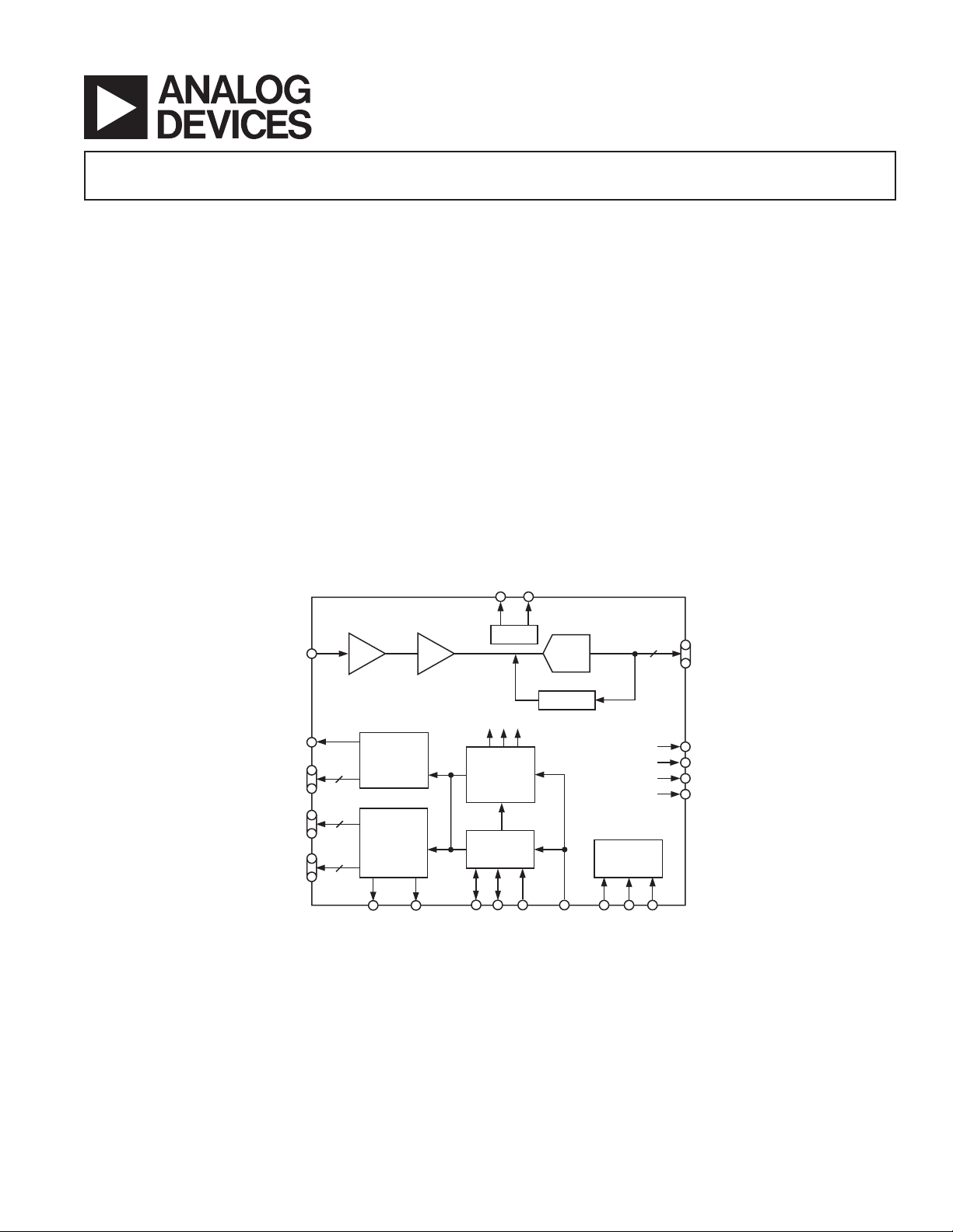
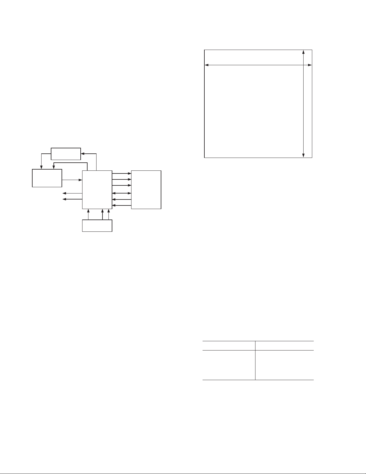
FUNCTIONAL BLOCK DIAGRAM
AD9898
CDS
6dB TO 40dB
VGA
GENERAL DESCRIPTION
The AD9898 is a highly integrated CCD signal processor for
digital still camera and digital video camera applications. It
includes a complete analog front end with A/D conversion
combined with a full function programmable timing generator.
A Precision Timing core allows adjustment of high speed clocks
with 1 ns resolution at 20 MHz operation.
The AD9898 is specified at pixel rates as high as 20 MHz. The
analog front end includes black level clamping, CDS, VGA, and
a 10-bit A/D converter. The timing generator provides all the
necessary CCD clocks: RG, H-clocks, V-clocks, sensor gate
pulses, substrate clock, and substrate bias pulse. Operation is
programmed using a 3-wire serial interface.
Packaged in a space saving 48-Lead LFCSP, the AD9898 is
specified over an operating temperature range of –20°C to +85°C.
REFT REFB
VREF
ADC
10
DOUT
INTERNAL CLOCKS
RG
H1, H2
V1, V2, V3, V4
VSG1, VSG2
HORIZONTAL
DRIVERS
2
4
V- H
CONTROL
2
VSUB SUBCK HD VD SYNC
REV. 0
Information furnished by Analog Devices is believed to be accurate and
reliable. However, no responsibility is assumed by Analog Devices for its
use, nor for any infringements of patents or other rights of third parties that
may result from its use. No license is granted by implication or otherwise
under any patent or patent rights of Analog Devices. Trademarks and
registered trademarks are the property of their respective companies.
CLAMP
DCLK1
PRECISION
TIMING
GENERATOR
SYNC
GENERATOR
CLI
One Technology Way, P.O. Box 9106, Norwood, MA 02062-9106, U.S.A.
Tel: 781/329-4700 www.analog.com
Fax: 781/326-8703 © 2003 Analog Devices, Inc. All rights reserved.
INTERNAL
REGISTERS
SL SCK SDATA
FD/DCLK2
MSHUT
STROBE
Page 2

AD9898
TABLE OF CONTENTS
FEATURES . . . . . . . . . . . . . . . . . . . . . . . . . . . . . . . . . . . . . 1
APPLICATIONS . . . . . . . . . . . . . . . . . . . . . . . . . . . . . . . . . 1
GENERAL DESCRIPTION . . . . . . . . . . . . . . . . . . . . . . . . . 1
FUNCTIONAL BLOCK DIAGRAM . . . . . . . . . . . . . . . . . 1
SPECIFICATIONS . . . . . . . . . . . . . . . . . . . . . . . . . . . . . . . 3
DIGITAL SPECIFICATIONS . . . . . . . . . . . . . . . . . . . . . . . 3
ANALOG SPECIFICATIONS . . . . . . . . . . . . . . . . . . . . . . . 4
TIMING SPECIFICATIONS . . . . . . . . . . . . . . . . . . . . . . . 5
ABSOLUTE MAXIMUM RATINGS . . . . . . . . . . . . . . . . . 6
ORDERING GUIDE . . . . . . . . . . . . . . . . . . . . . . . . . . . . . . 6
PIN CONFIGURATION . . . . . . . . . . . . . . . . . . . . . . . . . . . 7
PIN FUNCTION DESCRIPTIONS . . . . . . . . . . . . . . . . . . 7
SPECIFICATION DEFINITIONS . . . . . . . . . . . . . . . . . . . 8
Differential Nonlinearity (DNL) . . . . . . . . . . . . . . . . . . . . 8
Peak Nonlinearity . . . . . . . . . . . . . . . . . . . . . . . . . . . . . . . . 8
Total Output Noise . . . . . . . . . . . . . . . . . . . . . . . . . . . . . . 8
Power Supply Rejection (PSR) . . . . . . . . . . . . . . . . . . . . . . 8
EQUIVALENT INPUT CIRCUITS . . . . . . . . . . . . . . . . . . 8
TYPICAL PERFORMANCE CHARACTERISTICS . . . . . 9
SYSTEM OVERVIEW . . . . . . . . . . . . . . . . . . . . . . . . . . . . 16
CLI INPUT CLOCK DIVIDER . . . . . . . . . . . . . . . . . . . . . 16
GRAY CODE REGISTERS . . . . . . . . . . . . . . . . . . . . . . . . 16
SERIAL INTERFACE TIMING . . . . . . . . . . . . . . . . . . . . 17
Control Register Serial Interface . . . . . . . . . . . . . . . . . . . 17
System Register Serial Interface . . . . . . . . . . . . . . . . . . . . 17
Mode_A and Mode_B Register Serial Interface . . . . . . . . 17
VD SYNCHRONOUS AND ASYNCHRONOUS
REGISTER OPERATION . . . . . . . . . . . . . . . . . . . . . . . 18
Asynchronous Register Operation . . . . . . . . . . . . . . . . . . 18
VD Synchronous Register Operation . . . . . . . . . . . . . . . . 18
ANALOG FRONT END DESCRIPTION AND
OPERATION . . . . . . . . . . . . . . . . . . . . . . . . . . . . . . . . . 19
DC Restore . . . . . . . . . . . . . . . . . . . . . . . . . . . . . . . . . . . 19
Correlated Double Sampler . . . . . . . . . . . . . . . . . . . . . . . 19
PRECISION TIMING HIGH SPEED TIMING
GENERATION . . . . . . . . . . . . . . . . . . . . . . . . . . . . . . . . 19
Timing Resolution . . . . . . . . . . . . . . . . . . . . . . . . . . . . . . 19
High Speed Clock Programmability . . . . . . . . . . . . . . . . . 19
H-Driver and RG Outputs . . . . . . . . . . . . . . . . . . . . . . . . 20
Digital Data Outputs . . . . . . . . . . . . . . . . . . . . . . . . . . . . 20
EXTERNAL SYNCHRONIZATION (MASTER MODE) 23
HORIZONTAL AND VERTICAL SYNCHRONOUS
TIMING . . . . . . . . . . . . . . . . . . . . . . . . . . . . . . . . . . . . . 24
Special Note About the HDLEN Register . . . . . . . . . . . . 24
HORIZONTAL CLAMPING AND BLANKING . . . . . . . 25
Controlling CLPOB Clamp Pulse Timing . . . . . . . . . . . . 25
Controlling CLPOB Clamp Pulse Outputs . . . . . . . . . . . 26
H1 AND H2 BLANKING . . . . . . . . . . . . . . . . . . . . . . . . . 27
Normal H-Blanking . . . . . . . . . . . . . . . . . . . . . . . . . . . . . 27
Selective Positioning for Two H1 and H2 Outputs . . . . . 27
Extended Blanking . . . . . . . . . . . . . . . . . . . . . . . . . . . . . . 27
VGATE MASKING OF V1–V4 AND CLPOB
OUTPUTS . . . . . . . . . . . . . . . . . . . . . . . . . . . . . . . . . . . 29
VERTICAL TIMING GENERATION . . . . . . . . . . . . . . . 30
Creating Vertical Sequences . . . . . . . . . . . . . . . . . . . . . . . 30
Special Vertical Sweep Mode Operation . . . . . . . . . . . . . 34
Special Vertical Timing (SPAT) . . . . . . . . . . . . . . . . . . . 35
ELECTRONIC SHUTTER TIMING CONTROL . . . . . . 37
Normal Shutter Mode . . . . . . . . . . . . . . . . . . . . . . . . . . . 37
SUBCK Suppression Mode . . . . . . . . . . . . . . . . . . . . . . . 37
High Precision Shutter Mode . . . . . . . . . . . . . . . . . . . . . . 37
Single Pulse Mode . . . . . . . . . . . . . . . . . . . . . . . . . . . . . . 37
Multiple Pulse Mode . . . . . . . . . . . . . . . . . . . . . . . . . . . . 37
VSG TIMING . . . . . . . . . . . . . . . . . . . . . . . . . . . . . . . . . . . 40
VSUB CONTROL . . . . . . . . . . . . . . . . . . . . . . . . . . . . . . . 41
VSUB Placement and Polarity . . . . . . . . . . . . . . . . . . . . . 41
MSHUT CONTROL . . . . . . . . . . . . . . . . . . . . . . . . . . . . . 42
MSHUT Basic Operation . . . . . . . . . . . . . . . . . . . . . . . . 42
MSHUT High Precision Operation . . . . . . . . . . . . . . . . . 43
STROBE Control . . . . . . . . . . . . . . . . . . . . . . . . . . . . . . 44
SLAVE AND MASTER MODE OPERATION . . . . . . . . . 44
Slave Mode Operation . . . . . . . . . . . . . . . . . . . . . . . . . . . 44
Master Mode Operation . . . . . . . . . . . . . . . . . . . . . . . . . . 44
VARIABLE GAIN AMPLIFIER . . . . . . . . . . . . . . . . . . . . . 45
Optical Black Clamp . . . . . . . . . . . . . . . . . . . . . . . . . . . . 45
A/D Converter . . . . . . . . . . . . . . . . . . . . . . . . . . . . . . . . . 45
Digital I/O States for Different Operating Conditions . . . 45
POWER-UP . . . . . . . . . . . . . . . . . . . . . . . . . . . . . . . . . . . . 46
Recommended Power-Up Sequence for Master Mode . . . 46
STANDBY MODE OPERATION . . . . . . . . . . . . . . . . . . . 47
Recommended Standby Mode Sequence . . . . . . . . . . . . . 47
POWER-DOWN MODE OPERATION . . . . . . . . . . . . . . 48
Recommended Power-Down Sequence . . . . . . . . . . . . . . 48
HORIZONTAL TIMING SEQUENCE EXAMPLE . . . . . 49
CIRCUIT LAYOUT INFORMATION . . . . . . . . . . . . . . . 51
OUTLINE DIMENSIONS . . . . . . . . . . . . . . . . . . . . . . . . . 52
48-Lead LFCSP Package . . . . . . . . . . . . . . . . . . . . . . . . . 52
TABLES
Table I. Control Register Address Map . . . . . . . . . . . . . . . . 10
Table II. System Register Address Map . . . . . . . . . . . . . . . . 12
Table III. Mode_A Register Map . . . . . . . . . . . . . . . . . . . . . 14
Table IV. Mode_B Register Map . . . . . . . . . . . . . . . . . . . . . 15
Table V. Grade Code Registers . . . . . . . . . . . . . . . . . . . . . . 16
Table VI. Type of Serial Interface Registers . . . . . . . . . . . . 17
Table VII. AFE Registers . . . . . . . . . . . . . . . . . . . . . . . . . . 19
Table VIII. RG, H1, SHP, SHD, DCLK, and
DOUTPHASE Timing Parameters . . . . . . . . . . . . . . . . . 21
Table IX. Precision Timing Edge Locations for RG, H1, SHP,
SHD, DCLK, and DOUTPHASE . . . . . . . . . . . . . . . . . . 21
Table X. External Synchronization (Master Mode) . . . . . . . 23
Table XI. HD and VD Registers . . . . . . . . . . . . . . . . . . . . . 24
Table XII. CLPOB Registers . . . . . . . . . . . . . . . . . . . . . . . . 25
Table XIII. SCP and CLPEN . . . . . . . . . . . . . . . . . . . . . . . 26
Table XIV. H1 Blanking Registers . . . . . . . . . . . . . . . . . . . . 27
Table XV. V1–V4 Registers to Configure V1–V4 Pulse
for Each VTP Pattern . . . . . . . . . . . . . . . . . . . . . . . . . . . . 32
Table XVI. Mode_A and Mode_B Registers for VTPx
Selection . . . . . . . . . . . . . . . . . . . . . . . . . . . . . . . . . . . . . 33
Table XVII. Mode_A and Mode_B Registers for CCD
Region Selection . . . . . . . . . . . . . . . . . . . . . . . . . . . . . . . 33
Table XVIII. Description of SVREP_MODE Register . . . . 34
Table XIX. HD and VD Registers . . . . . . . . . . . . . . . . . . . . 35
Table XX. SPATLOGIC Register . . . . . . . . . . . . . . . . . . . . 35
Table XXI. SUBCK Registers . . . . . . . . . . . . . . . . . . . . . . . 37
Table XXII. Single and Multiple Pulse Mode . . . . . . . . . . . 37
Table XXIII. VSG Registers . . . . . . . . . . . . . . . . . . . . . . . . 40
Table XXIV. VSUB Registers . . . . . . . . . . . . . . . . . . . . . . . 41
Table XXV. MSHUT and STROBE Registers . . . . . . . . . . 42
Table XXVI. I/O Levels . . . . . . . . . . . . . . . . . . . . . . . . . . . . 45
REV. 0–2–
Page 3
AD9898
SPECIFICATIONS
Parameter Min Typ Max Unit
TEMPERATURE RANGE
Operating –20 +85 °C
Storage –65 +150 °C
POWER SUPPLY VOLTAGE
AVDD (AFE Analog Supply) 2.7 3.0 3.6 V
TCVDD (Timing Core Analog Supply) 2.7 3.0 3.6 V
RGVDD (RG Driver) 2.7 3.0 3.6 V
HVDD (H1–H2 Drivers) 2.7 3.0 3.6 V
DRVDD (Data Output Drivers) 2.7 3.0 3.6 V
DVDD (Digital) 2.7 3.0 3.6 V
POWER DISSIPATION
20 MHz, Typical Supply Levels, 100 pF H1–H2 Loading 150 mW
Power from HVDD Only* 36 mW
Power-Down Mode (AFE and Digital in Standby Operation) 3 mW
MAXIMUM CLOCK RATE (CLI)
AD9898 20 MHz
*The total power dissipated by the HVDD supply may be approximated using the equation
Total HVDD Power = (CLOAD × HVDD × Pixel Frequency) × HVDD × Number of H-Outputs Used
Actual HVDD power may be slightly higher than the calculated value because of stray capacitance inherent in the PCB layout/routing.
Specifications subject to change without notice.
DIGITAL SPECIFICATIONS
(RGVDD = HVDD = 2.7 V to 3.6 V, DVDD = DRVDD = 2.7 V to 3.6 V, CL = 20 pF, T
otherwise noted.)
MIN
to T
MAX
, unless
Parameter Symbol Min Typ Max Unit
LOGIC INPUTS
High Level Input Voltage V
Low Level Input Voltage V
High Level Input Current I
Low Level Input Current I
Input Capacitance C
IH
IL
IH
IL
IN
2.1 V
0.6 V
10 µA
10 µA
10 pF
LOGIC OUTPUTS (Except H and RG)
High Level Output Voltage @ IOH = 2 mA V
Low Level Output Voltage @ IOL = 2 mA V
OH
OL
2.2 V
0.5 V
RG and H-DRIVER OUTPUTS (H1–H2)
High Level Output Voltage @ Maximum Current V
Low Level Output Voltage @ Maximum Current V
OH
OL
VDD – 0.5 V
0.5 V
RG Maximum Output Current (Programmable) 15 mA
H1 and H2 Maximum Output Current (Programmable) 30 mA
Maximum Load Capacitance 100 pF
Specifications subject to change without notice.
REV. 0
–3–
Page 4
AD9898
ANALOG SPECIFICATIONS
(AVDD = 3.0 V, f
= 20 MHz, T
CLI
MIN
to T
, unless otherwise noted.)
MAX
Parameter Min Typ Max Unit Comments
CDS
Allowable CCD Reset Transient 500 mV Input Signal Characteristics
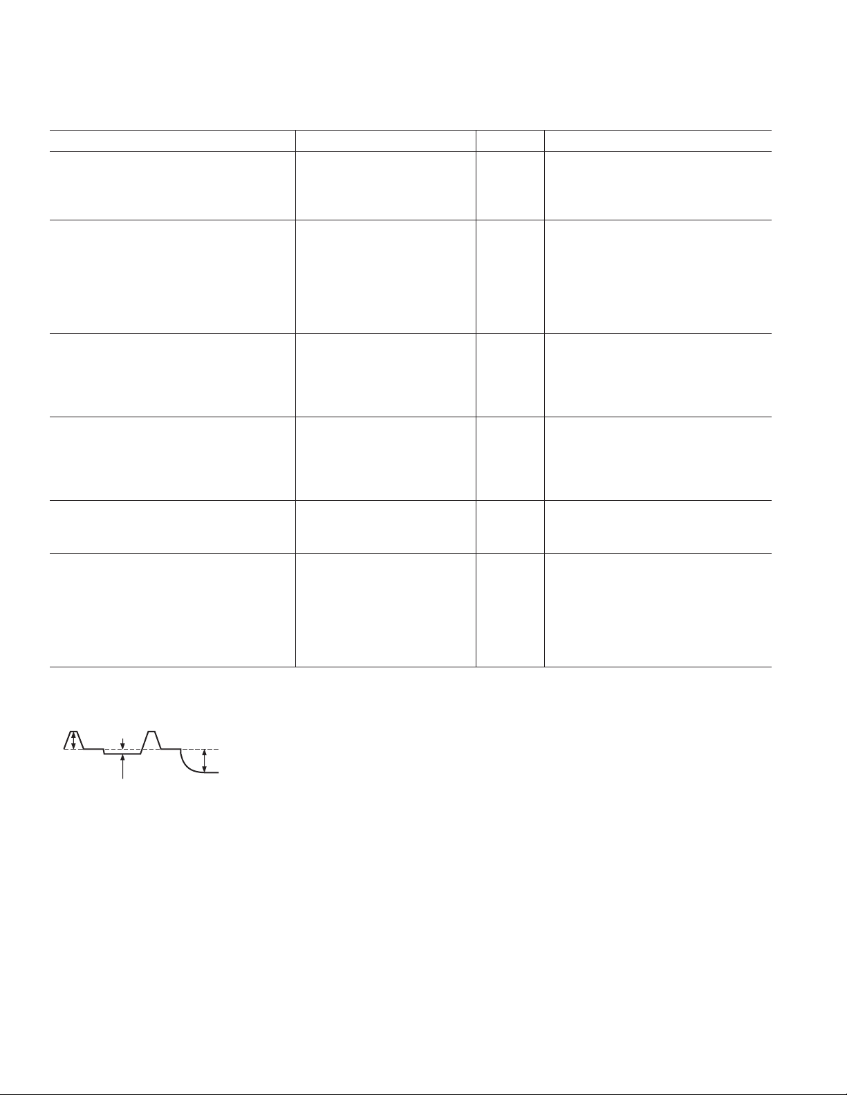
Maximum Input Range before Saturation* 1.0 V p-p
Maximum CCD Black Pixel Amplitude ± 100 mV
VARIABLE GAIN AMPLIFIER (VGA)
Maximum Output Range 2.0 V p-p
Gain Control Resolution 1024 Steps
Gain Monotonicity Guaranteed
Gain Range
Low Gain 6 dB
Maximum Gain 40 dB
BLACK LEVEL CLAMP
Clamp Level Resolution 64 Steps
Clamp Level LSB LSB is measured at ADC output.
Minimum Clamp Level 0 LSB
Maximum Clamp Level 63 LSB
A/D CONVERTER
Resolution 10 Bits
Differential Nonlinearity (DNL) ± 0.5 LSB
No Missing Codes Guaranteed
Full-Scale Input Voltage 2.0 V
VOLTAGE REFERENCE
Reference Top Voltage (REFT) 2.0 V
Reference Bottom Voltage (REFB) 1.0 V
SYSTEM PERFORMANCE Includes entire signal chain
Gain Accuracy
Low Gain (VGA Code = 20) 5 6 7 dB Gain = (0.035 × Code) + 5.3 dB
Maximum Gain (VGA Code = 991) 39 40 41 dB
Peak Nonlinearity, 500 mV Input Signal 0.1 % 12 dB gain applied
Total Output Noise 0.3 LSB rms AC grounded input, 6 dB gain applied
Power Supply Rejection (PSR) 40 dB Measured with step change on supply
*Input signal characteristics defined as follows:
500mV TYP
RESET
TRANSIENT
100mV MAX
OPTICAL
BLACK PIXEL
Specifications subject to change without notice.
1V MAX
INPUT
SIGNAL RANGE
REV. 0–4–
Page 5
AD9898
TIMING SPECIFICATIONS
(CL = 20 pF, AVDD = DVDD = DRVDD = 3.0 V, f
= 20 MHz, unless otherwise noted.)
CLI
Parameter Symbol Min Typ Max Unit
MASTER CLOCK, CLI
CLI Clock Period t
CONV
50 ns
CLI High/Low Pulsewidth 20 25 ns
Delay from CLI Rising Edge to Internal Pixel Position 0 t
CLIDLY
6ns
AFE CLAMP PULSES*
CLPOB Pulsewidth 4 10 Pixels
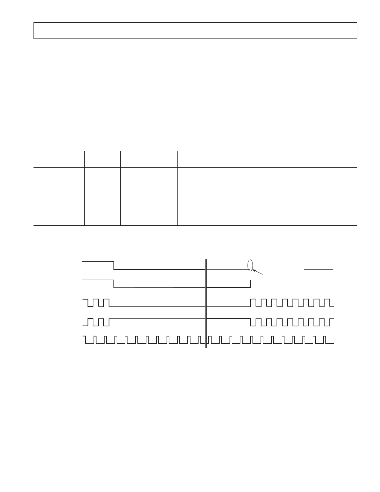
AFE SAMPLE LOCATION* (See Figure 13)
SHP Sample Edge to SHD Sample Edge t
S1
20 25 Pixels
DATA OUTPUTS (See Figure 15)
Output Delay from DCLK Rising Edge t
OD
9ns
Pipeline Delay from SHP/SHD Sampling 9 Cycles
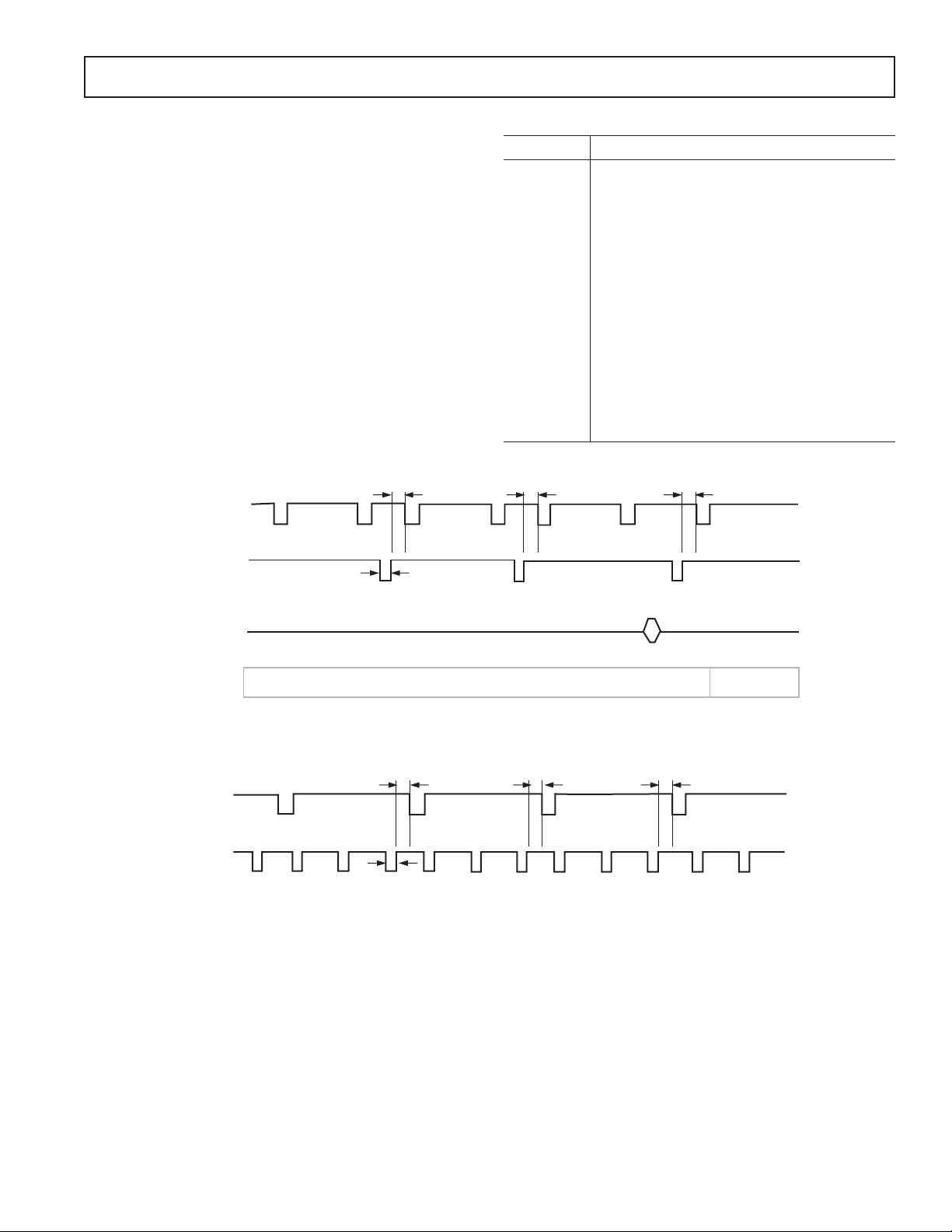
SERIAL INTERFACE (See Figures 7 and 8)
Maximum SCK Frequency f
SL to SCK Setup Time t
SCK to SL Hold Time t
SDATA Valid to SCK Rising Edge Setup t
SCK Falling Edge to SDATA Valid Hold t
SCK Falling Edge to SDATA Valid Read t
*Parameter is programmable.
Specifications subject to change without notice.
SCLK
LS
LH
DS
DH
DV
10 MHz
10 ns
10 ns
10 ns
10 ns
10 ns
REV. 0
–5–
Page 6
AD9898
ABSOLUTE MAXIMUM RATINGS*
Parameter With Respect To Min Max Unit
AVDD AVSS –0.3 +3.9 V
TCVDD TCVSS –0.3 +3.9 V
HVDD HVSS –0.3 +3.9 V
RGVDD RGVSS –0.3 +3.9 V
DVDD DVSS –0.3 +3.9 V
DRVDD DRVSS –0.3 +3.9 V
RG Output RGVSS –0.3 RGVDD + 0.3 V
H1–H2 Output HVSS –0.3 HVDD + 0.3 V
Digital Outputs DVSS –0.3 DVDD + 0.3 V
Digital Inputs DVSS –0.3 DVDD + 0.3 V
SCK, SL, SDATA DVSS –0.3 DVDD + 0.3 V
REFT, REFB AVSS –0.3 AVDD + 0.3 V
CCDIN AVSS –0.3 AVDD + 0.3 V
Junction Temperature 150 °C
Lead Temperature, 10 sec 300 °C
*Stresses above those listed under Absolute Maximum Ratings may cause permanent damage to the device. This is a stress rating only;
functional operation of the device at these or any other conditions above those listed in the operational sections of this specification is not
implied. Exposure to absolute maximum rating conditions for extended periods may affect device reliability.
PACKAGE THERMAL CHARACTERISTICS
Thermal Resistance
JA = 92°C/W
ORDERING GUIDE
Model Temperature Range Package Description Package Option
AD9898KCP-20 –20ºC to +85ºC Lead Frame Chip Scale Package (LFCSP) CP-48
AD9898KCPRL-20 –20ºC to +85ºC Lead Frame Chip Scale Package (LFCSP) CP-48
CAUTION
ESD (electrostatic discharge) sensitive device. Electrostatic charges as high as 4000 V readily
accumulate on the human body and test equipment and can discharge without detection. Although the
AD9898 features proprietary ESD protection circuitry, permanent damage may occur on devices
subjected to high energy electrostatic discharges. Therefore, proper ESD precautions are recommended
to avoid performance degradation or loss of functionality.
REV. 0–6–
Page 7
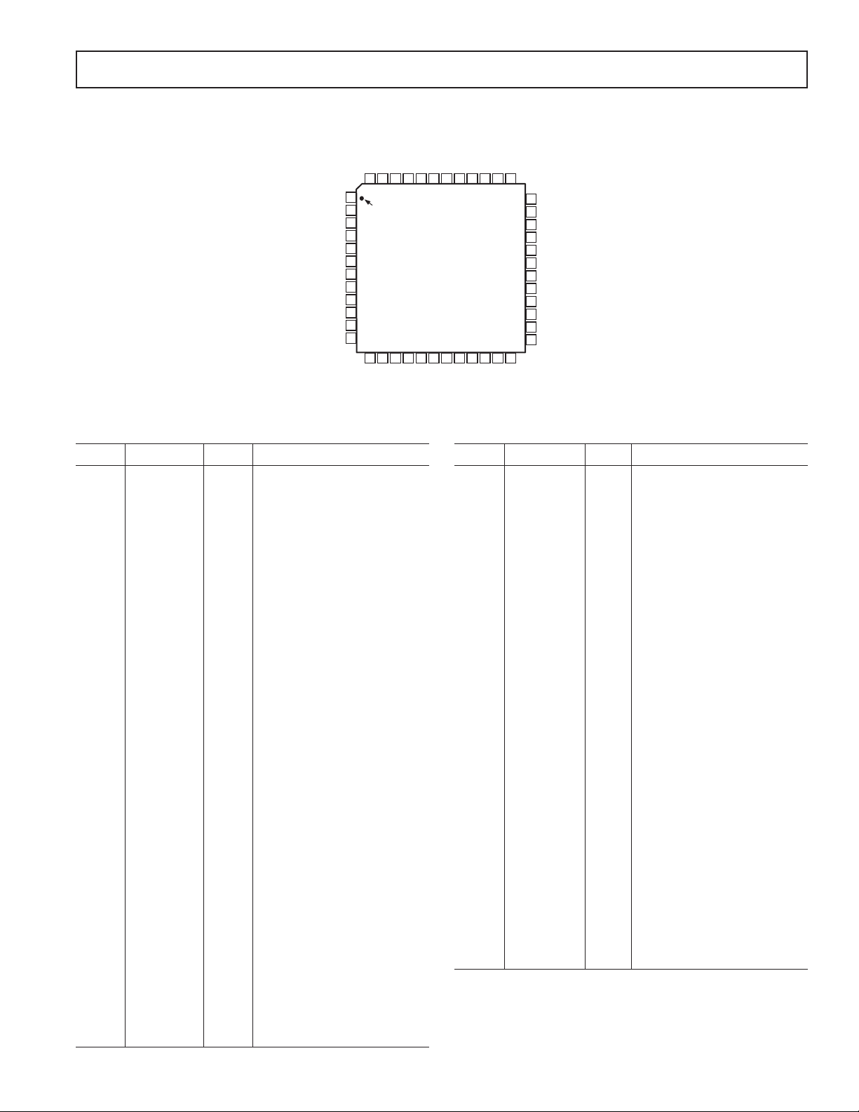
PIN CONFIGURATION
SUBCK
DVSS
DVD D
SYNC/VGATE
VSUB
OUTCONT
VSG2
HD
VSG1V4V3V2V1
VD
HVSS
HVDD
D0
D1
D2
D3
D4
DRVSS
DRVDD
D5
D6
D7
D8
D9
48 47 46 4 5 44 39 38 3743 4 2 41 40
1
PIN 1
2
IDENTIFIER
3
4
5
6
7
8
9
10
11
12
13 14 15 16 17 18 19 20 21 22 23 24
DCLK1
(Not to Scale)
MSHUT
STROBE
FD/DCLK2
AD9898
TOP VIEW
PIN FUNCTION DESCRIPTION
AD9898
36
SCK
35
SL
34
SDATA
33
REFB
32
REFT
31
AVSS
30
CCDIN
29
AV DD
28
CLI
27
TCVDD
26
TCVSS
25
RGVDD
H2
H1
RG
RGVSS
Pin No. Mnemonic Type* Description
1D0DOData Output
2D1DOData Output
3D2DOData Output
4D3DOData Output
5D4DOData Clock Output
6 DRVSS P Data Output Driver Ground
7 DRVDD P Data Output Driver Supply
8D5DOData Output
9D6DOData Output
10 D7 DO Data Output
11 D8 DO Data Output
12 D9 DO Data Output
13 DCLK1 DO Data Clock Output
14 MSHUT DO Mechanical Shutter Pulse
15 STROBE DO Strobe Pulse
16 FD/ DO Field Designator Output
DCLK2 DO DCLK2 Output
17 HD DI Horizontal Sync Pulse
18 VD DI Vertical Sync Pulse
19 HVDD P H1–H2 Driver Supply
20 HVSS P H1–H2 Driver Ground
21 H2 DO CCD Horizontal Clock 2
22 H1 DO CCD Horizontal Clock 1
23 RGVSS P RG Driver Ground
24 RG DO CCD Reset Gate Clock
25 RGVDD P RG Driver Supply
26 TCVSS P Analog Ground for Timing
Core
27 TCVDD P Analog Supply for Timing Core
Pin No. Mnemonic Type* Description
28 CLI DI Reference Clock Input
29 AVDD P Analog Supply for AFE
30 CCDIN AI CCD Input Signal
31 AVSS P Analog Ground for AFE
32 REFT AO Voltage Reference Top Bypass
33 REFB AO Voltage Reference Bottom
Bypass
34 SDATA DI 3-Wire Serial Data Input
35 SL DI 3-Wire Serial Load Pulse
36 SCK DI 3-Wire Serial Clock
37 V1 DO CCD Vertical Transfer Clock 1
38 V2 DO CCD Vertical Transfer Clock 2
39 V3 DO CCD Vertical Transfer Clock 3
40 V4 DO CCD Vertical Transfer Clock 4
41 VSG1 DO CCD Sensor Gate Pulse 1
42 VSG2 DO CCD Sensor Gate Pulse 2
43 OUTCONT DI Output Control
44 VSUB DO CCD Substrate Bias
45 SYNC/ DI External System Sync Input
VGATE DI VGATE Input
46 DVDD P Digital Supply for VSG,
V1–V4, HD, VD, MSHUT,
STROBE, and Serial Interface
47 DVSS P Digital Ground
48 SUBCK DO CCD Substrate Clock
(E-Shutter)
*AI = Analog Input, AO = Analog Output, DI = Digital Input, DO = Digital
Output, P = Power.
REV. 0
–7–
Page 8
AD9898
SPECIFICATION DEFINITIONS
Differential Nonlinearity (DNL)
An ideal ADC exhibits code transitions that are exactly 1 LSB
apart. DNL is the deviation from this ideal value. Thus every
code must have a finite width. No missing codes guaranteed to
10-bit resolution indicates that all 1024 codes, respectively,
must be present over all operating conditions.
Peak Nonlinearity
Peak nonlinearity, a full signal chain specification, refers to the
peak deviation of the output of the AD9898 from a true straight
line. The point used as zero scale occurs 1/2 LSB before the
first code transition. Positive full scale is defined as a level 1
1/2 LSB beyond the last code transition. The deviation is
measured from the middle of each particular output code to the
true straight line. The error is then expressed as a percentage of
the 2 V ADC full-scale signal. The input signal is always appropriately gained up to fill the ADC’s full-scale range.
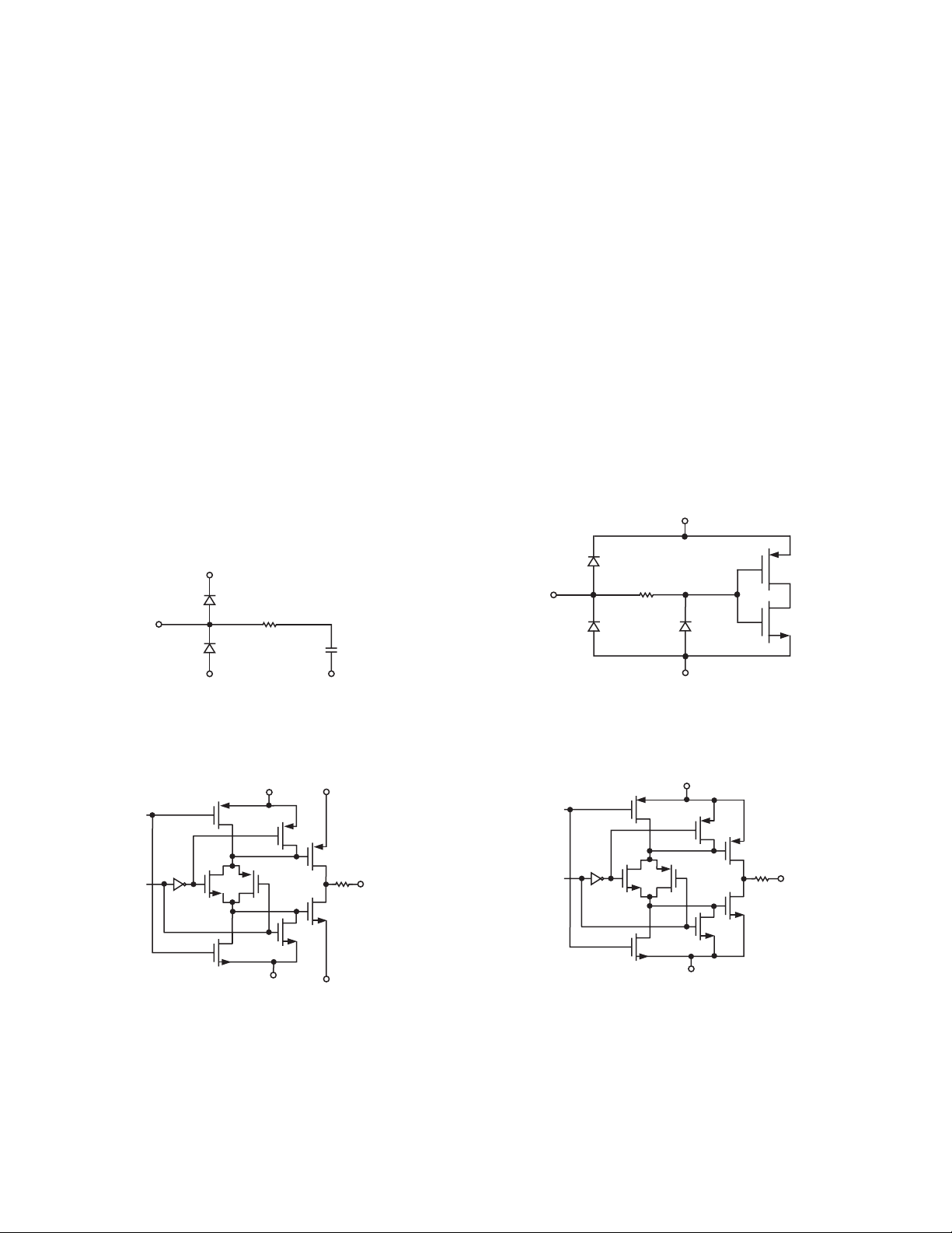
EQUIVALENT INPUT CIRCUITS
AVDD
Total Output Noise
The rms output noise is measured using histogram techniques.
The standard deviation of the ADC output codes is calculated
in LSB and represents the rms noise level of the total signal
chain at the specified gain setting. The output noise can be
converted to an equivalent voltage, using the relationship 1 LSB =
(ADC Full Scale/2
N
codes) where N is the bit resolution of the
ADC. For the AD9898, 1 LSB is 2 mV.
Power Supply Rejection (PSR)
The PSR is measured with a step change applied to the supply
pins. The PSR specification is calculated from the change in the
data outputs for a given step change in the supply voltage.
DVDD
330
AVSS
Figure 1. CCDIN
DVDD
DATA
THREESTATE
DVSS
Figure 2. Digital Data Outputs
R
AVSS
DVSS
Figure 3. Digital Inputs
HVDD OR
DRVDD
DRVSS
DOUT
RG,
H1–H2
ENABLE
RGVDD
OUTPUT
HVSS OR RGVSS
Figure 4. H1–H2, RG Drivers
REV. 0–8–
Page 9
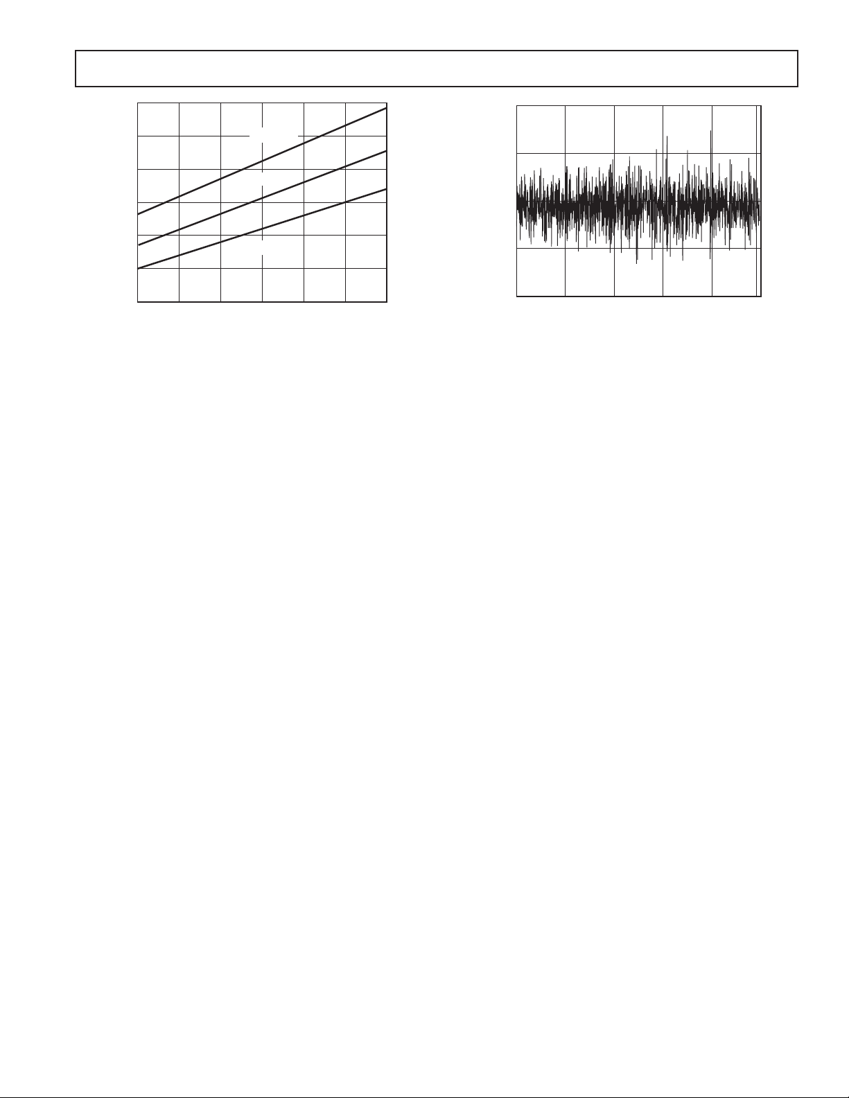
Typical Performance Characteristics–AD9898
180
160
140
120
100
POWER DISSIPATION (mW)
80
60
10
TPC 1. Power vs. Sample Rate
VDD = 3.3V
VDD = 3.0V
VDD = 2.7V
SAMPLE RATE – MHz
0.3
0.15
0
DNL (LSB)
–0.15
–0.3
2015
0
200 600 800
400
1000
CODE
TPC 2. Typical DNL Performance
REV. 0
–9–
Page 10

AD9898
Table I. Control Register Address Map (Register Names Are Subject to Change)
Bit Default Register
Address Content Width Value Name Register Description
00 (23:0) 23 000000 SW_RESET Software Reset = 000000. (Reset all registers to default.)
01 (23:21) 3 0 Unused
20 1 0 Unused. Test Mode. Should be set = 0.
(19:18) 2 1 Unused
17 1 1 HBLKMASK Masking Polarity for H1 during blanking period (0 = Low, 1 = High)
16 1 0 SYNCPOL External SYNC Active Polarity (0 = Active Low)
(15:14) 2 0 Unused
13 1 0 SUBCKMODE_HP High Precision Shutter Mode Operation (0 = Single Pulse, 1 = Multiple
Pulse)
12 1 0 SUBCKSUPPRESS Suppress First SUBCK after Last VSG Line Pulse (0 = No Suppression,
1 = Suppression of 1 SUBCK)
(11:10) 2 0 Unused
(9:8) 2 0 MSHUTPAT Selects MSHUT Pattern (See Figure 44) (0 = MSHUTPAT0,
1 = MSHUTPAT1, 2 = MSHUTPAT2, 3 = MSHUTPAT3)
710MSHUT/VGATE_EN MSHUT Masking of VGATE Input (0 = MSHUT does not mask
VGATE, 1 = MSHUT does mask VGATE)
610MSHUT/SUBCK_EN MSHUT Masking of SUBCK (0 = MSHUT does not mask SUBCK,
1 = MSHUT does mask SUBCK)
511CLP_CONT CLPOB Control (0 = CLPOB OFF, 1 = CLPOB ON)
411CLP_MODE CLPOB CCD Region Control (See Table XII)
(3:1) 3 0 Unused
010VDMODE VD Synchronous/Asynchronous Mode Setting (0 = VD Synchronous,
1 = VD Asynchronous)
02 (23:22) 2 0 Unused
(21:16) 6 0x34 SHDLOC SHD Sample Location
(15:14) 2 0 Unused
(13:8) 6 0x18 SHPLOC SHP Sample Location
(7:6) 2 0 DCLKPHASE DCLK Pulse Adjustment
(5:0) 6 0x0B DOUTPHASE Data Output [9:0] Phase Adjustment
03 (23:17) 7 0x00 Unused
16 1 0 H1BLKRETIME Retimes the H1 HBLK to Internal Clock
(15:14) 2 0 Unused
(13:8) 6 0x00 H1POSLOC H1 Positive Edge Location
(7:6) 2 0 Unused
(5:0) 6 0x10 RGNEGLOC RG Negative Edge Location
04 (23:22) 2 0 Unused
(21:16) 6 0x20 REFBLACK Black Clamp Level
(14:12) 3 5 H2DRV H2 Drive Strength (0 = Off, 1 = 4.3 mA, 2 = 8.6 mA, 3 = 12.9 mA,
4 = 17.2 mA, 5 = 21.5 mA, 6 = 25.8 mA, 7 = 30.1 mA)
11 1 0 Unused
(10:8) 3 5 H1DRV H1 Drive Strength (0 = Off, 1 = 4.3 mA, 2 = 8.6 mA, 3 = 12.9 mA,
4 = 17.2 mA, 5 = 21.5 mA, 6 = 25.8 mA, 7 = 30.1 mA)
(7:3) 5 0x00 Unused
(2:0) 3 2 RGDRV RG Drive Strength (0 = Off, 1 = 2.15 mA, 2 = 4.2 mA, 3 = 6.45 mA,
4 = 8.6 mA, 5 = 10.75 mA, 6 = 12.9 mA, 7 = 15.05 mA)
05 (23:10) 14 0x0000 Unused
910AFESTBY AFE Standby (0 = Standby , 1 = Normal Operation)
810DIGSTBY Digital Standby (0 = Standby , 1 = Normal Operation)
(7:2) 6 00 Unused
110OUTCONT_REG Internal OUTCONT Signal Control (0 = Digital Outputs held at fixed
dc level, 1 = Normal Operation)
011OUTCONT_ENB External OUTCONT Signal Input Pin 43 Control (0 = Pin Enabled,
1 = Pin Disabled)
REV. 0–10–
Page 11
AD9898
Table I. Control Register Address Map (Register Names Are Subject to Change)
Bit Default Register
Address Content Width Value Name Register Description
0A 23 1 0 Unused
22 1 0 FDPOL FD Polarity Control (0 = Low, 1 = High)
(21:16) 6 0x00 VSGMASK VSG Masking (See Table XXIII)
(15:12) 4 0 SYNCCNT External SYNC Setting
(VD (11:10) 2 0 SVREP_MODE Super Vertical Repetition Mode
SyncReg)* 910HBLKEXT H Pulse Blanking Extend Control
810HPULSECNT H Pulse Control during Blanking
(7:4) 4 C SPATLOGIC SPAT Logic Setting (See Table XX)
(3:2) 2 3 SVOS Second V Output Setting (10 = Output Repetition 1)
110SPAT_EN SPAT Control (0 = SPAT Disable, 1 = SPAT Enable)
010MODE Mode Control Bit (0 = Mode_A, 1 = Mode_B)
0B (23:22) 2 0 Unused
21 1 1 SUBCK_EN SUBCK Output Enable Control (0 = Disable, 1 = Enable)
20 1 1 VSG_EN VSG Output Enable Control (0 = Disable, 1 = Enable)
(VD (19:17) 3 0 Unused
SyncReg)* 16 1 0 STROBE_EN STROBE Output Control (0 = STROBE Output Held Low,
1 = STROBE Output Enabled)
15 1 0 Unused
(14:12) 3 0 SUBCKNUM_HP High Precision Shutter SUBCLK Pulse Position/Number
11 1 0 Unused
(10:0) 11 0x7FF SUBCKNUM Total Number of SUBCKs per Field
0C (23:21) 3 0 Unused
20 1 0 MSHUTINIT MSHUT Initialize (1 = Forces MSHUT Low)
(19:18) 2 0 Unused
(VD 17 1 0 Unused
SyncReg)* 16 1 0 MSHUTEN MSHUT Control ( 0 = MSHUT Held at Last State, 1 = MSHUT Output)
15 1 0 Unused
(14:12) 3 0 MSHUTPOS_HP MSHUT Position during High Precision Operation
11 1 0 Unused
(10:0) 11 0x000 MSHUTPOS MSHUT Position during Normal Operation
0D (23:17) 7 Unused
16 1 0 VSUBPOL VSUB Active Polarity (0 = Low, 1 = High)
(VD (15:11) 5 Unused
SyncReg)* (10:0) 11 0x000 VSUBTOG VSUB Toggle Position. Active starting line in any field.
0E (23:21) 3 0 Unused
20 1 0 Unused. Test Mode. Should be set = 0.
(19:18) 2 0 Unused
(VD 17 1 0 Unused. Test Mode. Should be set = 0.
SyncReg)* 16 1 0 Unused. Test Mode. Should be set = 0.
(15:10) 6 0x00 Unused
(9:0) 10 0x000 VGAGAIN VGA Gain
D5 (23:4) 20 0x00000 Unused
311DCLK2SEL DCLK2 Selector (0 = Select Internal FD Signal to be Output on FD/
DCLK2 Pin 16, 1 = Select CLI to be Output on FD/DCLK2 Pin 16)
210DCLK1SEL DCLK1 Selector (0 = Select DLL Version for DCLK1 Output,
1 = Select CLI for DCLK1 Output)
(1:0) 2 0 CLKDIV Input Clock Divider (0 = No Division, 1 = 1/2, 2 = 1/3, 3 = 1/4)
D6 (23:1) 23 0x000000 Unused
011SLAVE_MODE Operating Mode ( 0 = Master Mode, 1 = Slave Mode)
*This register defaults to VD synchronous mode type at power up. VD sync type registers do not get updated until the first falling edge of VD is asserted after the
register has been programmed. VD sync type registers can be programmed to be asynchronous registers by setting VDMODE = 1 (Addr 0x01).
REV. 0
–11–
Page 12

AD9898
Table II. System Register Address Map (Addr 0x14)
Bit Default
Register Content Width (Decimal) Register Name Register Description
Sys_Reg(0) (31:24) 8 NA System_Reg_Addr System Register Address Is (Addr 0x14)
(23:0) 24 NA System_Number_N Number N Register Writes (0x000000 = Write All Registers)
Sys_Reg(1) (31:23) 9 37 VTPLEN0 Vertical Sequence No. 0: Length between Repetitions
22 1 0 V1STARTPOL0 Vertical Sequence No. 0: V1 Start Polarity
21 1 0 V2STARTPOL0 Vertical Sequence No. 0: V2 Start Polarity
20 1 1 V3STARTPOL0 Vertical Sequence No. 0: V3 Start Polarity
19 1 1 V4STARTPOL0 Vertical Sequence No. 0: V4 Start Polarity
(18:10) 9 0 V1TOG1POS0 Vertical Sequence No. 0: V1 Toggle Position 1
(9:1) 9 19 V1TOG2POS0 Vertical Sequence No. 0: V1 Toggle Position 2
010 V2TOG1POS0 [8]
Sys_Reg(2) (31:24) 8 12 V2TOG1POS0 [7:0] Vertical Sequence No. 0: V2 Toggle Position 1
(23:15) 9 31 V2TOG2POS0 Vertical Sequence No. 0: V2 Toggle Position 2
(14:6) 9 0 V3TOG1POS0 Vertical Sequence No. 0: V3 Toggle Position 1
(5:0) 6 V3TOG2POS0 [8:3]
Sys_Reg(3) (31:29) 3 19 V3TOG2POS0 [2:0] Vertical Sequence No. 0: V3 Toggle Position 2
(28:20) 9 12 V4TOG1POS0 Vertical Sequence No. 0: V4 Toggle Position 1
(19:11) 9 31 V4TOG2POS0 Vertical Sequence No. 0: V4 Toggle Position 2
(10:2) 9 104 VTPLEN1 Vertical Sequence No. 1: Length between Repetitions
110 V1STARTPOL1 Vertical Sequence No. 1: V1 Start Polarity
010 V2STARTPOL1 Vertical Sequence No. 1: V2 Start Polarity
Sys_Reg(4) 31 1 1 V3STARTPOL1 Vertical Sequence No. 1: V3 Start Polarity
30 1 1 V4STARTPOL1 Vertical Sequence No. 1: V4 Start Polarity
(29:21) 9 18 V1TOG1POS1 Vertical Sequence No. 1: V1 Toggle Position 1
(20:12) 9 58 V1TOG2POS1 Vertical Sequence No. 1: V1 Toggle Position 2
(11:3) 9 47 V2TOG1POS1 Vertical Sequence No. 1: V2 Toggle Position 1
(2:0) 3 V2TOG2POS1 [8:6]
Sys_Reg(5) (31:26) 6 96 V2TOG2POS1 [5:0] Vertical Sequence No. 1: V2 Toggle Position 2
(25:17) 9 0 V3TOG1POS1 Vertical Sequence No. 1: V3 Toggle Position 1
(16:8) 9 76 V3TOG2POS1 Vertical Sequence No. 1: V3 Toggle Position 2
(7:0) 8 V4TOG1POS1 [8:1]
Sys_Reg(6) 31 1 38 V4TOG1POS1 [0] Vertical Sequence No. 1: V4 Toggle Position 1
(30:22) 9 105 V4TOG2POS1 Vertical Sequence No. 1: V4 Toggle Position 2
(21:13) 9 57 VTPLEN2 Vertical Sequence No. 2: Length between Repetitions
12 1 0 V1STARTPOL2 Vertical Sequence No. 2: V1 Start Polarity
11 1 0 V2STARTPOL2 Vertical Sequence No. 2: V2 Start Polarity
10 1 1 V3STARTPOL2 Vertical Sequence No. 2: V3 Start Polarity
911 V4STARTPOL2 Vertical Sequence No. 2: V4 Start Polarity
(8:0) 9 0 V1TOG1POS2 Vertical Sequence No. 2: V1 Toggle Position 1
Sys_Reg(7) (31:23) 9 29 V1TOG2POS2 Vertical Sequence No. 2: V1 Toggle Position 2
(22:14) 9 19 V2TOG1POS2 Vertical Sequence No. 2: V2 Toggle Position 1
(13:5) 9 48 V2TOG2POS2 Vertical Sequence No. 2: V2 Toggle Position 2
(4:0) 5 V3TOG1POS2 [8:4]
Sys_Reg(8) (31:28) 4 0 V3TOG1POS2 [3:0] Vertical Sequence No. 2: V3 Toggle Position 1
(27:19) 9 29 V3TOG2POS2 Vertical Sequence No. 2: V3 Toggle Position 2
(18:10) 9 19 V4TOG1POS2 Vertical Sequence No. 2: V4 Toggle Position 1
(9:1) 9 48 V4TOG2POS2 Vertical Sequence No. 2: V4 Toggle Position 2
01 Unused
REV. 0–12–
Page 13
AD9898
Table II. System Register Address Map (Addr 0x14) (continued)
Bit Default
Register Content Width (Decimal) Register Name Register Description
Sys_Reg(9) (31:23) 9 89 VTPLEN3 Vertical Sequence No. 3: Length between Repetitions
22 1 0 V1STARTPOL3 Vertical Sequence No. 3: V1 Start Polarity
21 1 0 V2STARTPOL3 Vertical Sequence No. 3: V2 Start Polarity
20 1 1 V3STARTPOL3 Vertical Sequence No. 3: V3 Start Polarity
19 1 1 V4STARTPOL3 Vertical Sequence No. 3: V4 Start Polarity
(18:10) 9 0 V1TOG1POS3 Vertical Sequence No. 3: V1 Toggle Position 1
(9:1) 9 60 V1TOG2POS3 Vertical Sequence No. 3: V1 Toggle Position 2
01 V2TOG1POS3 [8]
Sys_Reg(10) (31:24) 8 30 V2TOG1POS3 [7:0] Vertical Sequence No. 3: V2 Toggle Position 1
(23:15) 9 90 V2TOG2POS3 Vertical Sequence No. 3: V2 Toggle Position 2
(14:6) 9 0 V3TOG1POS3 Vertical Sequence No. 3: V3 Toggle Position 1
(5:0) 6 V3TOG2POS3 [8:3]
Sys_Reg(11) (31:29) 3 60 V3TOG2POS3 [2:0] Vertical Sequence No. 3: V3 Toggle Position 2
(28:20) 9 30 V4TOG1POS3 Vertical Sequence No. 3: V4 Toggle Position 1
(19:11) 9 90 V4TOG2POS3 Vertical Sequence No. 3: V4 Toggle Position 2
(10:1) 10 0 HBLKHPOS H1 Pulse ON Position during Blanking Period
01 Unused
Sys_Reg(12) (31:20) 12 2283 HDLEN* 12-Bit Gray Code HD Counter Value (Gray Code Number)
(19:10) 10 130 HLEN 10-Bit HL Counter Value
(9:1) 9 100 OLEN 9-Bit OL Counter Value
01 BLLEN [8]
Sys_Reg(13) (31:24) 8 0 BLLEN[7:0] 9-Bit BL Counter Value
(23:16) 8 118 MSHUTLEN MSHUT Sequence Length
(15:5) 11 1048 VSGTOG1_0 VSG Sequence No. 1 Toggle Position 1
(4:0) 5 VSGTOG1_1 [10:6]
Sys_Reg(14) (31:26) 6 1198 VSGTOG1_1 [5:0] VSG Sequence No. 2 Toggle Position 1
(25:18) 8 60 VSGLEN VSG Pulsewidth
(17:9) 9 19 SUBCK1TOG1 SUBCK1 First Toggle Position
(8:0) 9 88 SUBCK1TOG2 SUBCK1 Second Toggle Position
Sys_Reg(15) (31:23) 9 19 SUBCK2TOG1 SUBCK2 First Toggle Position
(22:14:) 9 88 SUBCK2TOG2 SUBCK2 Second Toggle Position
(13:2) 12 2243 CLPTOG1* CLPOB Toggle Position No. 1
(1:0) 2 CLPTOG2 [11]*
Sys_Reg(16) (31:22) 10 2278 CLPTOG2 [10:0]* CLPOB Toggle Position No. 2
(21:18) 4 9 VDRISE VD Toggle Position No. 1
(17:8) 10 120 HDRISE HD Toggle Position No. 2
(7:0) 8 Unused
*Register value must be a gray code number. (See Gray Code Registers section.)
REV. 0
–13–
Page 14

AD9898
Table III. Mode_A Register Map (Addr 0x15)
Bit Default
Register Content Width (Decimal) Register Name Register Description
Mode_Reg(0) (31:24) 8 NA Mode_A_Addr Mode_A Address Is (Addr 0x15)
(23:0) 24 NA Mode_A_Number_N Number N Register Writes (0x000000 = Write All Registers)
Mode_Reg(1) (31:21) 11 262 VDLEN VD Counter Value
(20:9) 12 1139 HDLASTLEN Number of Pixels in Last Line (Gray Code Number)
811 VSGSEL0 VSG1 Sequence Selector (See Table XXIII)
710 VSGSEL1 VSG2 Sequence Selector (See Table XXIII)
(6:0) 7 0 VSGACTLINE VSG Active Line
Mode_Reg(2) 31 1 0 SUBCKSEL Select one of two SUBCK Patterns
(30:28) 3 0 VTPSEQPTR0 Vertical Transfer Sequence Region No. 0
(27:25) 3 0 VTPSEQPTR1 Vertical Transfer Sequence Region No. 1
(24:22) 3 0 VTPSEQPTR2 Vertical Transfer Sequence Region No. 2
(21:19) 3 0 VTPSEQPTR3 Vertical Transfer Sequence Region No. 3
(18:16) 3 0 VTPSEQPTR4 Vertical Transfer Sequence Region No. 4
15 1 1 CLPEN0 CLPOB Output Control No. 1
14 1 0 CLPEN1 CLPOB Output Control No. 2
13 1 0 CLPEN2 CLPOB Output Control No. 3
12 1 0 CLPEN3 CLPOB Output Control No. 4
11 1 0 CLPEN4 CLPOB Output Control No. 5
(10:3) 8 0 SCP1 Sequence Change Position No. 1
(2:0) 3 SCP2
Mode_Reg(3) (31:27) 5 0 SCP2 Sequence Change Position No. 2
(26:19) 8 0 SCP3 Sequence Change Position No. 3
(18:11) 8 0 SCP4 Sequence Change Position No. 4
(10:9) 2 0 VTPSEL0 Vertical Pattern Selection 0
(8:7) 2 0 VTPSEL1 Vertical Pattern Selection 1
(6:5) 2 0 VTPSEL2 Vertical Pattern Selection 2
(4:3) 2 0 VTPSEL3 Vertical Pattern Selection 3
(2:0) 3 3 VTPREP0 Number of Vertical Pulse Repetitions for Pattern0
Mode_Reg(4) (31:29) 3 0 VTPREP1 Number of Vertical Pulse Repetitions for Pattern1
(28:26) 3 0 VTPREP2 Number of Vertical Pulse Repetitions for Pattern2
(25:23) 3 0 VTPREP3 Number of Vertical Pulse Repetitions for Pattern3
(22:12) 11 0 SVREP0 Vertical Sweep Repetition Number for CCD Region0
(11:1) 11 0 SVREP3 Vertical Sweep Repitition Number for CCD Region3
01 Unused
Mode_Reg(5) (31:19) 13 988 V1SPAT_TOG1 Polarity Change Position Start for V1 SPAT
(18:6) 13 1138 V1SPAT_TOG2 Polarity Change Position End for V1 SPAT
(5:0) 6 V2SPAT_TOG1
Mode_Reg(6) (31:25) 7 1078 V2SPAT_TOG1 Polarity Change Position Start for V2 SPAT
(24:12) 13 1168 V2SPAT_TOG2 Polarity Change Position End for V2 SPAT
(11:0) 12 V3SPAT_TOG1
Mode_Reg(7) 31 1 958 V3SPAT_TOG1 Polarity Change Position Start for V3 SPAT
(30:18) 13 1138 V3SPAT_TOG2 Polarity Change Position End for V3 SPAT
(17:5) 13 988 V4SPAT_TOG1 Polarity Change Position Start for V4 SPAT
(4:0) 5 V4SPAT_TOG2
Mode_Reg(8) (31:24) 8 1228 V4SPAT_TOG2 Polarity Change Position End for V4 SPAT
(23:11) 13 1392 SECONDVPOS Second V Pattern Output Position
(10:9) 2 3 VPATSECOND Selected Second V Pattern Group for VSG Active Line
(8:0) 9 Unused
REV. 0–14–
Page 15

AD9898
Table IV. Mode_B Register Map (Addr 0x16)
Bit Default
Register Content Width (Decimal) Register Name Register Description
Mode_Reg(0) (31:24) 8 NA Mode_B_Addr Mode_B Address Is (Addr 0x16)
(23:0) 24 NA Mode_B_Number_N Number N Register Writes (0x000000 = Write All Registers)
Mode_Reg(1) (31:21) 11 262 VDLEN VD Counter Value
(20:9) 12 1139 HDLASTLEN* Number of Pixels in Last Line (Gray Code Number)
811 VSGSEL0 VSG1 Sequence Selector (See Table XXIII)
710 VSGSEL1 VSG2 Sequence Selector (See Table XXIII)
(6:0) 7 0 VSGACTLINE VSG Active Line
Mode_Reg(2) 31 1 0 SUBCKSEL Select One of Two SUBCK Patterns
(30:28) 3 0 VTPSEQPTR0 Vertical Transfer Sequence Region No. 0
(27:25) 3 0 VTPSEQPTR1 Vertical Transfer Sequence Region No. 1
(24:22) 3 0 VTPSEQPTR2 Vertical Transfer Sequence Region No. 2
(21:19) 3 0 VTPSEQPTR3 Vertical Transfer Sequence Region No. 3
(18:16) 3 0 VTPSEQPTR4 Vertical Transfer Sequence Region No. 4
15 1 1 CLPEN0 CLPOB Output Control No. 1
14 1 0 CLPEN1 CLPOB Output Control No. 2
13 1 0 CLPEN2 CLPOB Output Control No. 3
12 1 0 CLPEN3 CLPOB Output Control No. 4
11 1 0 CLPEN4 CLPOB Output Control No. 5
(10:3) 8 0 SCP1 Sequence Change Position No. 1
(2:0) 3 SCP2
Mode_Reg(3) (31:27) 5 0 SCP2 Sequence Change Position No. 2
(26:19) 8 0 SCP3 Sequence Change Position No. 3
(18:11) 8 0 SCP4 Sequence Change Position No. 4
(10:9) 2 0 VTPSEL0 Vertical Pattern Selection 0
(8:7) 2 0 VTPSEL1 Vertical Pattern Selection 1
(6:5) 2 0 VTPSEL2 Vertical Pattern Selection 2
(4:3) 2 0 VTPSEL3 Vertical Pattern Selection 3
(2:0) 3 3 VTPREP0 Number of VTP0 Pulse Repetitions for Pattern0
Mode_Reg(4) (31:29) 3 0 VTPREP1 Number of VTP1 Pulse Repetitions for Pattern1
(28:26) 3 0 VTPREP2 Number of VTP2 Pulse Repetitions for Pattern2
(25:23) 3 0 VTPREP3 Number of VTP0 Pulse Repetitions for Pattern3
(22:12) 11 0 SVREP0 Vertical Sweep Repetition Number for CCD Region0
(11:1) 11 0 SVREP3 Vertical Sweep Repetition Number for CCD Region3
01 Unused
Mode_Reg(5) (31:19) 13 988 V1SPAT_TOG1 Polarity Change Position Start for V1 SPAT
(18:6) 13 1138 V1SPAT_TOG2 Polarity Change Position End for V1 SPAT
(5:0) 6 V2SPAT_TOG1
Mode_Reg(6) (31:25) 7 1078 V2SPAT_TOG1 Polarity Change Position Start for V2 SPAT
(24:12) 13 1168 V2SPAT_TOG2 Polarity Change Position End for V2 SPAT
(11:0) 12 V3SPAT_TOG1
Mode_Reg(7) 31 1 958 V3SPAT_TOG1 Polarity Change Position Start for V3 SPAT
(30:18) 13 1138 V3SPAT_TOG2 Polarity Change Position End for V3 SPAT
(17:5) 13 988 V4SPAT_TOG1 Polarity Change Position Start for V4 SPAT
(4:0) 5 V4SPAT_TOG2
Mode_Reg(8) (31:24) 8 1228 V4SPAT_TOG2 Polarity Change Position End for V4 SPAT
(23:11) 13 1392 SECONDVPOS Second V Pattern Output Position
(10:9) 2 3 VPATSECOND Selected Second V Pattern Group for VSG Active Line
(8:0) 9 Unused
*Register value must be a gray code number. (See Gray Code Registers section.)
REV. 0
–15–
Page 16
AD9898
SYSTEM OVERVIEW
Figure 5 shows the typical system block diagram for the AD9898.
The CCD output is processed by the AD9898’s AFE circuitry,
which consists of a CDS, VGA, black level clamp, and A/D
converter. The digitized pixel information is sent to the digital
image processor chip, which performs the postprocessing and
compression. To operate the CCD, all CCD timing parameters
are programmed into the AD9898 from the system microprocessor, through the 3-wire serial interface. From the system
master clock, CLI, provided by the image processor or external
crystal, the AD9898 generates all the CCD’s horizontal and
vertical clocks and all internal AFE clocks. External synchronization is provided by a SYNC pulse from the microprocessor,
which will reset internal counters and resynchronize the VD and
HD outputs.
V-DRIVER
H1, H2, RG, VSUB
CCD
MSHUT
STROBE
V1–V4, VSG1, VSG2, SUBCK
CCDIN
AD9898
SERIAL
INTERFACE
SYNC
P
DOUT[9:0]
DCLK1
FD
HD, VD
VGATE
CLI
OUTCONT
DIGITAL
IMAGE
PROCESSING
ASIC
Figure 5. Typical System Block Diagram, Master Mode
The AD9898 powers up in slave mode, in which the VD and
HD are provided externally from the image processor. In this
mode, all AD9898 timing will be synchronized with VD and
HD. The H-drivers for H1–H2 and RG are included in the
AD9898, allowing these clocks to be directly connected to the
CCD. H-drive voltage of up to 3.6 V is supported. An external
V-driver is required for the vertical transfer clocks, the sensor
gate pulses, and the substrate clock. The AD9898 also includes
programmable MSHUT and STROBE outputs, which may be
used to trigger mechanical shutter and strobe (flash) circuitry.
Figure 6 shows the horizontal and vertical counter dimensions
for the AD9898. All internal horizontal and vertical clocking is
programmed using these dimensions and is used to specify line
and pixel locations.
MAXIMUM FIELD DIMENSIONS
12-BIT HORIZONTALCOUNTER = 4096 PIXELS MAX
11-BIT VERTICAL COUNTER = 2048 LINES MAX
Figure 6. Horizontal and Vertical Counters
CLI INPUT CLOCK DIVIDER
The AD9898 provides the capability of dividing the CLI input
clock using register CLKDIV (Addr 0xD5). The following
procedure must be followed to reset the AFE and digital circuits
when CLKDIV is reprogrammed back to 0 from CLKDIV = 1,
2, or 3. The DCLK1 output will become unstable if this procedure is not followed:
Step 1: CLKDIV = 1, 2, or 3 (CLI divided by setting value)
Step 2: CLKDIV = 0 (CLI reprogrammed for no division)
Step 3: DIGSTBY = AFESTBY = 0
Step 4: DIGSTBY = AFESTBY = 1
GRAY CODE REGISTERS
Table V lists the AD9898 registers requiring gray code values.
Below is an example of applying a gray code number for
HDLEN using a line length of 1560 pixels:
HDLEN = (1560 – 4) = 1556
10
(See Table XI note about HDLEN.)
1556
= 0x51E
10
The gray code value of 0x51E would be programmed in the
12-bit HDLEN register.
Table V. Gray Code Registers
Register Name Register Type
HDLEN System_Reg(12)
CLPTOG1 System_Reg(15)
CLPTOG2 System_Reg(15 and 16)
HDLASTLEN Mode_Reg(1)
REV. 0–16–
Page 17

AD9898
SERIAL INTERFACE TIMING
All of the internal registers of the AD9898 are accessed through a
3-wire serial interface. The interface consists of a clock (SCK),
serial load (SL), and serial data (SDATA).
The AD9898 has three different register types that are configured by the 3-wire serial interface. They are control registers,
system registers, and mode registers and are described in Table VI.
Table VI. Type of Serial Interface Registers
Register Address No. of Registers
Control 0x00 through There is a 24-bit register at each
0xD6 address. Not all addresses are
used. See Table I.
System 0x14 Seventeen 32-bit system registers
at Address 0x14. See Table II.
Mode_A 0x15 Eight 32-bit Mode_A registers at
Address 0x15. See Table III.
Mode_B 0x16 Eight 32-bit Mode_B registers at
Address 0x16. See Table IV.
Control Register Serial Interface
The control register 3-wire interface timing requirements are
shown in Figure 7. Control data must be written into the device
one address at a time due to the noncontiguous address spacing
for the control registers. This requires eight bits of address data
followed by 24 bits of configuration data between each active
low period of SL for each address. The SL signal must be kept
high for at least one full SCK cycle between successive writes to
control registers.
System Register Serial Interface
There are seventeen 32-bit system registers that get accessed
sequentially at Address 0x14 beginning with Sys_Reg[0]. When
writing to the system registers, SDATA contains the 8-bit address
of 0x14, followed by Number Writes N[23:0], followed by the
Sys_Reg[31:0] data as shown in Figure 8. The system register
map is listed in Table II.
There are two options available when writing to the system
registers. The choice is automatically determined by the value of
the Number Writes N[23:0] word. If Number Writes N[23:0] =
0x000000, the device gets put into a mode where it expects all
17 Sys_Reg[31:0] data-words to be clocked in before SL is
asserted high. If the Number Writes N[23:0] is decoded as
some number N other than 0x000000, the device expects N
number of registers to be programmed where N is equal to the
value of Number Writes N[23:0]. For example, if Number
Writes N[23:0] = 0x000004, the device would expect data to be
provided for Sys_Reg[3:0]. In all cases, the system registers
would be written to begin with Sys_Reg[0], no matter what the
value of Number Writes N[23:0] is. Note that SL can be brought
high or low during access to system registers, as shown in Figure 8.
Mode_A and Mode_B Register Serial Interface
There are eight 32-bit Mode_A and eight 32-bit Mode_B registers that get accessed sequentially at Address 0x15 and Address
0x16, respectively. The Mode_A and Mode_B registers get
written to exactly as the system registers are. (See the description above.) The mode registers are listed in Tables III and IV.
Changing operation between Mode_A and Mode_B is done by
setting the 1-bit MODE register (Addr 0x0A). The desired
Mode_A (Addr 0x15) or Mode_B (Addr 0x16) data must be
programmed into the Mode_A or Mode_B registers before
changing the MODE bit.
SDATA
SCK
SL
A7 A4 A3 A2 A1 A0
t
DS
1234567891011 29303132
t
1. SDATA BITS ARE INTERNALLY LATCHED ON THE RISING EDGES OF SCK.
2. SYSTEM UPDATE OF LOADED REGISTERS OCCURS ON SL RISING EDGE.
3. THIS TIMING PATTERN MUST BE WRITTEN FOR EACH REGISTER WRITE WITH SL REMAINING HIGH FOR AT
LEAST ONE FULL SCK PERIOD BEFORE ASSERTING SL LOW AGAIN FOR THE NEXT REGISTER WRITE.
A5A6 D22 D21 D3 D2 D1
t
DH
LS
D23
Figure 7. 3-Wire Serial Interface Timing for Control Registers
....
....
D0
t
LH
REV. 0
–17–
Page 18

AD9898
ADDRESS [7:0]
SDATA
SCK
A7A6A5A4A3A2A1
8-BIT
ADDRESS
SL
1. ALL SL PULSES ARE IGNORED UNTIL THE LSB OF THE LAST DATA N WORD IS CLOCKED IN.
2. VALID SL PULSE. SL MUST BE ASSERTED HIGH WHEN ALL SDI DATA TRANSMISSIONS HAVE BEEN FINISHED.
NUMBER WRITES N [23:0]
A0
N21
N20
N22
N23
NUMBER OF 32-BIT
DATA WRITES (N)
N1
N2
N3
N0
D31
DATA 1 [31:0]
D29
D30
DATA 1 [31:0]
1
D3D2D1
DATA 2 [31:0] DATA N [31:0]
D0
D31
D30
D29
DATA 2 [31:0]
1
Figure 8. System and Mode Register Writes
OPERATION OF VD SYNCHRONOUS TYPE
REGISTER WRITES BEGIN AT THE NEXT VD
FALLING EDGE.
VD
HD
D3D2D1
D0
D31
D30
12
D3D2D1
D29
DATA N [31:0]
D0
CLI
PROGRAMMING OF VD SYNCHRONOUS
TYPE REGISTERS MUST BE COMPLETED
AT LEAST 4 CLI CYCLES BEFORE THE
FALLING EDGE OF VD.
Figure 9. VD Synchronous Type Register Writes
VD SYNCHRONOUS AND ASYNCHRONOUS REGISTER OPERATION
There are two types of control registers, VD synchronous and
VD asynchronous, as indicated in the address column of Table I.
Register writes to synchronous and asynchronous type registers
operate differently, as described below. Writes to system, Mode_A,
and Mode_B registers occur asynchronously.
Asynchronous Register Operation
For VD asynchronous register writes, SDATA data is stored
directly into the serial register at the rising edge of SL. As a
result, register operation begins immediately after the rising
edge of SL.
VD Synchronous Register Operation
For VD synchronous type registers, SDATA data is temporarily
stored in a buffer register at the rising edge of SL. This data is
held in the buffer register until the next falling edge of VD is
applied. Once the next falling edge of VD occurs, the buffered
SDATA data is loaded into the serial register and the register
operation begins (see Figure 9).
All control registers at the following addresses are VD Synchronous type registers—Addr: 0x0A, 0x0B, 0x0C, 0x0D, and 0x0E
(see Table I).
REV. 0–18–
Page 19

AD9898
ANALOG FRONT END (AFE) DESCRIPTION AND OPERATION
The AD9898 AFE signal processing chain is shown in Figure 10.
Each processing step is essential to achieving a high quality image
from the raw CCD pixel data. Registers for the AD9898 AFE
section are listed in Table VII.
DC Restore
To reduce the large dc offset of the CCD output signal, a dc
restore circuit is used with an external 0.1 µF series coupling
capacitor. This restores the dc level of the CCD signal to approximately 1.5 V, which is compatible with the 3 V analog supply of
the AD9898.
Correlated Double Sampler
To extract the video information and reject low frequency noise,
the CDS circuit samples each CCD pixel twice. The timing
shown in Figure 12 illustrates how the two internally generated
CDS clocks, SHP and SHD, are used to sample the reference
level and the data level of the CCD signal, respectively. The
placement of the SHP and SHD sampling edges is determined
by the setting of the SHPLOC (Addr 0x02) and SHDLOC
(Addr 0x02) registers. Placement of these two clock edges is critical to achieving the best performance from the CCD.
Table VII. AFE Registers
Register Bit
Name Width Register Type Description
VGAGAIN 10 Control (Addr 0x0E) VGA Gain
REFBLACK 6 Control (Addr 0x04) Blk Clamp Level
AFESTBY 1 Control (Addr 0x05) AFE Standby
PRECISION TIMING HIGH SPEED TIMING GENERATION
The AD9898 generates flexible high speed timing signals using
the Precision Timing core. This core is the foundation for generating the timing used for both the CCD and the AFE signals,
including the reset gate RG, the horizontal drivers H1–H2, and
the CDS sample clocks. By providing precise control over the
horizontal CCD readout and the AFE correlated double sampling,
the unique architecture of the AD9898 makes optimizing image
quality a routine task for a system designer.
Timing Resolution
The Precision Timing core uses a 1× master clock input (CLI)
as a reference. This clock should be the same as the CCD pixel
clock frequency. Figure 11 illustrates how the internal timing
core divides the master clock period into 48 steps or edge positions. Using a 20 MHz CLI frequency for the AD9898, the
edge resolution of the Precision Timing core is 1 ns. A 40 MHz
CLI frequency can be applied where the AD9898 will internally divide the CLI frequency by two. Division by one-third
and one-fourth is also provided. CLI frequency division is controlled using the CLKDIV (Addr 0xD5) register.
High Speed Clock Programmability
Figure 13 shows how the high speed clocks RG, H1–H2, SHP,
and SHD are generated. The RG pulse has a fixed rising edge
and a programmable falling edge. The horizontal clock H1
has a programmable rising and a fixed falling edge occurring at
H1POSLOC + 24 steps. The H2 clock is always the inverse of
H1. Table VIII summarizes the high speed timing registers and
the parameters for the high speed clocks. Each register is six bits
wide with the 2 MSB used to select the quadrant region as
outlined in Table VIII. Figure 13 shows the range and default locations of the high speed clock signals.
0.1F
CCDIN
DC RESTORE
1.5V
SHP
CDS
AD9898
SHD
VGA GAIN
REGISTER
SHD
SHP
PRECISION
TIMING
GENERATION
6dB TO 40dB
VGA
10
DOUT
PHASE
8-BIT
DAC
Figure 10. AFE Block Diagram
REFB
1.0V
OPTICAL BLACK
DIGITAL
FILTER
CLPOB
V-H
TIMING
GENERATION
1.0F
INTERNAL
V
REF
2V FULL
SCALE
ADC
CLAMP
1.0F
REFT
2.0V
CLPOB
6
CLAMP LEVEL
REGISTER
OUTPUT
DATA
LATCH
DOUT
PHASE
10
DOUT
REV. 0
–19–
Page 20

AD9898
H-Driver and RG Outputs
In addition to the programmable timing positions, the AD9898
features on-chip output drivers for the RG and H1–H2 outputs.
They are sufficiently powerful to directly drive the CCD inputs.
The H-driver current can be adjusted for optimum rise/fall time
into a particular load by using the H1DRV and H2DRV registers (Addr 0x04). The RG drive current is adjustable using the
RGDRV register (Addr 0x04). The H1DRV and H2DRV register is adjustable in 4.3 mA increments. The RGDRV register is
adjustable in 2.15 mA increments. All DRV registers have a setting
of 0 equal to OFF or three-state, and the maximum setting of 7.
POSITION
CLI
t
CLIDLY
1 PIXEL
PERIOD
1. PIXEL CLOCK PERIOD IS DIVIDED INTO 48 POSITIONS, PROVIDING FINE EDGE RESOLUTION FOR HIGH SPEED CLOCKS.
2. THERE IS A FIXED DELAY FROM THE CLI INPUT TO THE INTERNAL PIXEL PERIOD POSITIONS (
P[0] P[48] = P[0]P[12] P[24] P[36]
Figure 11. High Speed Clock Resolution from CLI Master Clock Input
3
CCD
SIGNAL
4
As shown in Figure 13, the H2 output is the inverse of H1. The
internal propagation delay resulting from the signal inversion is
less than 1 ns, which is significantly less than the typical rise
time driving the CCD load. This results in an H1/H2 crossover
voltage of approximately 50% of the output swing. The crossover voltage is not programmable.
Digital Data Outputs
The AD9898 DOUT[9:0] and DCLK phases are independently
programmable using the DOUTPHASE register (Addr 0x02)
and DCLKPHASE register (Addr 0x02) (see Figure 15).
t
= 6 ns TYP).
CLIDLY
cds
(INTERNAL)
RG
H1
H2
12
56
PROGRAMMABLE CLOCK POSITIONS
1. RG RISING EDGE (FIXED EDGE AT 000000).
2. RG FALLING EDGE (RGNEGLOC (ADDR 0x03)).
3. SHP SAMPLE LOCATION (SHPLOC (ADDR 0x02)).
4. SHD SAMPLE LOCATION (SHDLOC (ADDR 0x02)).
5. H1 RISING EDGE LOCATION (H1POSLOC (ADDR 0x03))
6. H1 NEGATIVE EDGE LOCATION (FIXED AT (H1POSLOC + 24 STEPS)).
7. H2 IS ALWAYS THE INVERSE OF H1.
Figure 12. High Speed Clock Programmable Locations
REV. 0–20–
Page 21

AD9898
Table VIII. RG, H1, SHP, SHD, DCLK, and DOUTPHASE Timing Parameters
Register Name Bit Width Register Type Range Description
RGNEGLOC 6 Control (Addr 0x03) 0–47 Edge Location Falling Edge Location for RG
H1POSLOC 6 Control (Addr 0x03) 0–47 Edge Location Positive Edge Location for H1
SHPLOC 6 Control (Addr 0x02) 0–47 Edge Location Sample Location for SHP
SHDLOC 6 Control (Addr 0x02) 0–47 Edge Location Sample Location for SHD
DOUTPHASE 6 Control (Addr 0x02) 0–47 Edge Location Phase Location of Data Output [9:0]
DCLKPHASE 6 Control (Addr 0x02) 0–47 Edge Location Positive Edge of DCLK 1
The 2 MSB are used to select the quadrant.
Table IX. Precision Timing Edge Locations for RG, H1, SHP, SHD, DCLK, and DOUTPHASE
RG Rising Edge RG Falling Edge
Signal Name Quadrant (Not Programmable) RGNEGLOC Quadrant Range
RG I Fixed at 000000 000000 to 001011 P[0] to P[11]
II Fixed at 000000 010000 to 011011 P[12] to P[23]
III Fixed at 000000 100000 to 101011 P[24] to P[35]
IV Fixed at 000000 110000 to 111011 P[36] to P[47]
H1 Rising Edge H1 Falling Edge
Signal Name Quadrant H1POSLOC Quadrant Range (Not Programmable)
H1 I 000000 to 001011 P[0] to P[11] H1POSLOC + 24 Steps
II 010000 to 011011 P[12] to P[23] H1POSLOC + 24 Steps
III 100000 to 101011 P[24] to P[35] H1POSLOC + 24 Steps
IV 110000 to 111011 P[36] to P[47] H1POSLOC + 24 Steps
cds Rising Edge cds Falling Edge
Signal Name Quadrant SHPLOC Quadrant Range SHDLOC Quadrant Range
cds I 000000 to 001011 P[0] to P[11] 000000 to 001011 P[0] to P[11]
II 010000 to 011011 P[12] to P[23] 010000 to 011011 P[12] to P[23]
III 100000 to 101011 P[24] to P[35] 100000 to 101011 P[24] to P[35]
IV 110000 to 111011 P[36] to P[47] 110000 to 111011 P[36] to P[47]
Data Output[9:0] Rising Edge Data Output[9:0] Falling Edge
Signal Name Quadrant DOUTPHASE Quadrant Range (Not Programmable)
Data Output[9:0] I 000000 to 001011 P[0] to P[11] DOUTPHASE + 24 Steps
II 010000 to 011011 P[12] to P[23] DOUTPHASE + 24 Steps
III 100000 to 101011 P[24] to P[35] DOUTPHASE + 24 Steps
IV 110000 to 111011 P[36] to P[47] DOUTPHASE + 24 Steps
Signal Name DCLKPHASE Value DCLKPHASE Rising Edge DCLKPHASE Falling Edge
DCLK1 00 P[6] P[26]
01 P[16] P[36]
10 P[26] P[06]
11 P[36] P[16]
REV. 0
–21–
Page 22

AD9898
POSITION
PIXEL
PERIOD
RG
H1
cds
(INTERNAL)
CCD
SIGNAL
P[0]
RGf[12]RGr[0]
Hr[0]
SHP[20]
1. ALL SIGNAL EDGES ARE FULLY PROGRAMMABLE TO ANY OF THE 48 POSITIONS WITHIN ONE PIXEL PERIOD.
2. DEFAULT POSITIONS FOR EACH SIGNAL ARE SHOWN.
P[24]P[12] P[36]
Hf[24]
t
S1
SHD[40]
P[48] = P[0]
Figure 13. High Speed Clock Default and Programmable Locations
t
H1
H2
RISE
t
<
t
PD
RISE
FIXED CROSSOVER VOLTAGE
H1
Figure 14. H-Clock Inverse Phase Relationship
P[0] P[48] = P[0]
PIXEL
PERIOD
DCLK1
t
OD
DOUT
1. DCLK1 PHASE IS ADJUSTED BY SETTING THE DCLKPHASE REGISTER (ADDR 0x02).
2. DOUT PHASE CAN BE ADJUSTED BY SETTING THE DOUTPHASE REGISTER (ADDR 0x02).
P[12] P[24] P[36]
Figure 15. Digital Output Phase Adjustment
t
PD
H2
REV. 0–22–
Page 23
AD9898
EXTERNAL SYNCHRONIZATION (MASTER MODE)
External synchronization can be used to synchronize the VD
and HD signal by applying an external pulse on the SYNC/
VGATE pin (Pin 45) for master mode operation. The SYNC/
VGATE pin is configured as an external SYNC input for master mode operation by setting the SLAVE_MODE register
(Addr 0xD6) = 0. (The AD9898 defaults to slave mode at
power-up.)
SYNCCNT (Addr 0x0A) and SYNCPOL (Addr 0x01) are the
only two registers used for configuring the AD9898 for external
synchronization. The SYNCPOL is a 1-bit register used for
configuring the SYNC input as either active low or active high.
The AD9898 defaults to active low at power-up. The function
of the SYNCCNT register is described in Table X. Figures 16
and 17 provide two examples of external synchronization with
SYNCPOL = 0.
4 CLI 4 CLI 4 CLI
VD
Table X. External Synchronization (Master Mode)
SYNCCNT External Synchronization Options
0Disable External Synchronization
1 VD Sync at every SYNC Pulse
2 VD Sync after Second Applied SYNC Pulse
3 VD Sync after Third Applied SYNC Pulse
4 VD Sync after Fourth Applied SYNC Pulse
5 VD Sync after Fifth Applied SYNC Pulse
6 VD Sync after Sixth Applied SYNC Pulse
7 VD Sync after Seventh Applied SYNC Pulse
8 VD Sync after Eighth Applied SYNC Pulse
9 VD Sync after Ninth Applied SYNC Pulse
10 VD Sync after Tenth Applied SYNC Pulse
11 VD Sync after Eleventh Applied SYNC Pulse
12 VD Sync after Twelfth Applied SYNC Pulse
13 VD Sync after Thirteenth Applied SYNC Pulse
14 VD Sync after Fourteenth Applied SYNC Pulse
15 VD Sync after First Applied SYNC Pulse Only
SYNC
SERIAL
WRITES
OPERATION
MODE
VD
SYNC
2 CLI
MIN
CHANGE TO MODE B
MODE A MODE B
Figure 16. Example of Synchronization with SYNCPOL = 0 and SYNCCNT = 1
4 CLI4 CLI4 CLI
2 CLI
MIN
Figure 17. Example of Synchronization with SYNCPOL = 0 and SYNCCNT = 3
REV. 0
–23–
Page 24

AD9898
HORIZONTAL AND VERTICAL SYNCHRONOUS TIMING
The HD and VD output pulses are programmable using the
registers listed in Table XI. The HD output is asserted low at
the start of the horizontal line shift. The VD output is asserted
low at the start of each line. As shown in Figure 18, the 11-bit
VD counter is used to count the number of lines set by the
VDLEN register. The 12-bit HD counter is used to count the
number of pixels in each line set by the HDLEN register. For
example, if the CCD array size is 2000 lines by 2100 pixels per
line, VDLEN = 2000 and HDLEN = 0xC28. The HLEN regis-
Special Note about the HDLEN Register
The 12-bit HD counter value must be programmed using a gray
code number. There is also a 4-clock cycle setup period that
must be considered when determining the HDLEN register
value, as shown in Figure 18. As a result of the 4-clock cycle
setup period, the value of HDLEN is always equal to the actual
number of pixels per line minus four. For example, if there are
2100 pixels per line, HDLEN equals (2100 – 4) = 2096. The
gray code value of 2096 is 0xC28, which is what would be pro-
grammed in the HDLEN register.
ter sets the HL counter that is used as a reference for the rising
edge of the HD pulse.
Table XI. HD and VD Registers
Register Bit Reference
Name Width Register Type Counter Range Description
HDLEN 12 Sys_Reg(12) 0–4095 Pixels 12-Bit Gray Code Counter Value
HLEN 10 Sys_Reg(12) 0–1023 Pixels 10-Bit HL Counter Value
HDRISE 10 Sys_Reg(16) HL 0–1023 Pixels HD Rise Position
HDLASTLEN* 12 Mode_Reg(1) HD 0–4095 Pixels HD Last Line Length
VDLEN 11 Mode_Reg(1) 0–2047 Lines VD Counter Value
VDRISE 4 Sys_Reg(16) VD 0–15 Lines VD Rise Position
*Register value must be a gray code number. (See Gray Code Registers section.)
11-BIT
VD COUNTER
GRAY COUNTER
12-BIT
+ SETUP
10-BIT
HL COUNTER
VD
HD
VDLEN
001000 002
HLEN
2
1
LINE LENGTH =
HDLEN + 4
1. THE SETUP DELAY IS 4 CLI CYCLES. THE ACTUAL LENGTH OF ONE LINE IS 4
MORE CYCLES THAN THE VALUE SET IN HDLEN AND HDLASTLEN DUE TO SETUP DELAY.
2. VDRISE REFERENCES THE 11-BIT VD COUNTER.
3. HDRISE REFERENCES THE 10-BIT HL COUNTER.
PROGRAMMABLE CLOCK POSITIONS
1. HDRISE (SYS_REG(16))
2. VDRISE (SYS_REG(16))
Figure 18. VD and HD Horizontal Timing
N
2048
HDLASTLENSETUPHDLEN
REV. 0–24–
Page 25

AD9898
Table XII. CLPOB Registers
Register Bit Reference
Name Width Register Type Counter Range Description
CLP_CONT 1 Control (0x01) CLPOB Control (0 = CLPOB Off, 1 = CLPOB On)
CLP_MODE 1 Control(0x01) CLPOB CCD Region Control
(0 = Enable CLPENx Register Settings,
1 = Disable CLPENx Register Settings)
CLPTOG1 12 Sys_Reg(15) HD 0–4095 Pixel Locations CLPOB Toggle Position 1 (Gray Code Number)
CLPTOG2 12 Sys_Reg(15 and 16) HD 0–4095 Pixel Locations CLPOB Toggle Position 2 (Gray Code Number)
CLPEN0 1 Mode_Reg(2) CLPOB Control for CCD Region 0
(0 = CLPOB Disabled, 1 = CLPOB Enabled)
CLPEN1 1 Mode_Reg(2) CLPOB Control for CCD Region 1
(0 = CLPOB Disabled, 1 = CLPOB Enabled)
CLPEN2 1 Mode_Reg(2) CLPOB Control for CCD Region 2
(0 = CLPOB Disabled, 1 = CLPOB Enabled)
CLPEN3 1 Mode_Reg(2) CLPOB Control for CCD Region 3
(0 = CLPOB Disabled, 1 = CLPOB Enabled)
CLPEN4 1 Mode_Reg(2) CLPOB Control for CCD Region 4
(0 = CLPOB Disabled, 1 = CLPOB Enabled)
VD
HD
12-BIT
GRAY COUNTER
+ SETUP
CLPOB
PROGRAMMABLE CLOCK POSITIONS
1. CLPTOG1 (SYS_REG(15))
2. CLPTOG2 (SYS_REG(15 AND 16))
Figure 19. Location of CLPOB Using CLPTOG1 and CLPTOG2 Registers
HORIZONTAL CLAMPING AND BLANKING
The AD9898’s horizontal clamping and blanking pulses are
programmable to suit a variety of applications. Similar to vertical timing generation, individual sequences are defined for each
signal and are then organized into multiple regions during
image readout. This allows the dark pixel clamping and blanking
patterns to be changed at each stage of the readout to accommodate different image transfer timing and high speed line shifts.
Controlling CLPOB Clamp Pulse Timing
The AFE horizontal CLPOB pulse is generated based on the
12-bit gray code counter. Once the length of the 12-bit gray
code counter is set using the HDLEN register (Sys_Reg(12)),
CLPTOG1 and CLPTOG2 registers (Sys_Reg(15 and16)) can
be used to place the CLPOB pulse location, as shown in Figure 19.
Table XII lists all CLPOB registers that are used to configure
and control the placement and output of the CLPOB pulse.
The length of the last HD line is set using the HDLASTLEN
register (Sys_Reg(1)). Figure 20 shows that no CLPOB pulse
will be asserted when the last HD length set by HDLASTLEN
is shorter than the regular HD length set by HDLEN.
12
Figure 21 shows that no CLPOB pulse will be applied when the
last HD length set by HDLASTLEN is longer than the regular
HD length. Note that the CLPOB pulse is applied in the last
line only when HDLASTLEN = HDLEN.
HD
CLPOB
LAST LINE
Figure 20. Last HD Shorter Than Regular HD
HD
CLPOB
LAST LINE
Figure 21. Last HD Longer Than Regular HD
REV. 0
–25–
Page 26

AD9898
Controlling CLPOB Clamp Pulse Outputs
The registers in Table XII are used for programming the CLPOB
pulse, which will be disabled in all CCD regions by setting
CLPCNT = 0. The CLPTOGx (x = 0, 1) are used to set the
CLPOB toggle positions. The CLPENx (x = 0, 1, 2, 3, and 4)
are used to enable or disable the CLPOB pulse separately in
each CCD region when CLPMODE = 0. The CLPEN registers have no effect if CLPMODE = 1. In this case, the CLPOB
pulse will be asserted in all CCD regions, regardless of the value
set in the CLPENx registers.
Figure 22 shows an example of the CLPOB pulse being disabled
in CCD Regions 1 and 3 by setting CLPEN1 = 1 and CLPEN3
= 1. Note that the CLPOB pulse remains disabled in the first
line of the following CCD region.
VD
HD
CLPOB
CLPMASK
(INTERNAL)
PROGRAMMING POSITIONS
1. SCP0 = 0 (FIXED), CLPEN0 = 1
2. SCP1 = 3, CLPEN1 = 0
3. SCP2 = 4, CLPEN2 = 1
4. SCP3 = 5, CLPEN3 = 0
5. SCP4 = 1, CLPEN4 = 1
NOTE
THE INTERNAL CLPMASK SIGNAL EXTENDS ONE EXTRA HD CYCLE FROM THE TIME WHEN THE
CLPMASK PERIOD CHANGES FROM LOW TO HIGH. AS A RESULT, ONE ADDITIONAL CLPOB PULSE
IS MASKED, AS SHOWN AT POSITIONS A AND B.
1
02345678910111213141516
AB
1
23 45
Figure 22. CLPOB Outputs with CLPMODE = 0
Table XIII. SCP and CLPEN
SCP[4:1] CLPEN[4:0]
SCP0* CLPEN0
SCP1 CLPEN1
SCP2 CLPEN2
SCP3 CLPEN3
SCP4 CLPEN4
*SCP0 is not a programmable register and therefore is not listed in the register
map tables. SCP0 is a fixed sequence and always starts at the falling edge of
VD. Although this register is not programmable, the CLPEN0 register is still
used to enable or disable the CLPOB pulse for the SCP0 region.
REV. 0–26–
Page 27
AD9898
H1 AND H2 BLANKING
The AD9898 provides three options for controlling the period
where H1 and H2 pulses get blanked. These options are normal
H blanking, selective positioning for 2 H1 and H2 outputs, and
extended blanking. In all cases, HBLKMASK is used to set the
polarity of H1 during the blanking period. Table XIV describes
the registers used to control H blanking.
Normal H Blanking
For normal H blanking operation, HPULSECNT = 0 and
BLKMASK = 0 or 1. The HBLKHPOS register is not used in
Selective Positioning for Two H1 and H2 Outputs
For selective positioning operation, HPULSECNT = 1 and
HBLKMASK = 0 or 1. In this mode, two H1 pulses are output
during the blanking period. The location of these two pulses are
set using the HBLKHPOS register, as shown in Figure 24.
Extended Blanking
Extended blanking is enabled by setting HBLKEXT = 1. The
HBLKEXT register uses the 9-bit BL counter to suspend operation
of the HD and HL counters. This delays the blanking period by
the length set in the BLLEN register as shown in Figure 25.
this mode. Figure 23 shows one example where HBLKMASK = 0.
As seen in Figure 23, H1 and H2 are blanked while HD is Low.
Table XIV. H1 Blanking Registers
Register Bit
Name Width Register Type Description
1
HBLKMASK 1 Control (0x01) Masking Polarity for H1 during Blanking Period
(0 = Low, 1 = High)
HPULSECNT 1 Control (0x0A) H Pulse Control during Blanking Period
(0 = No Output during Blanking, 1 = Output during Blanking)
HBLKEXT 1 Control (0x0A) H Pulse Blanking Extend Control
2
(0 = Extended Blanking Disabled, 1 = Extended Blanking Enabled)
H1BLKRETIME 1 Control (0x03) Retimes the H1 HBLK to Internal Clock
(0 = Retiming Disabled, 1 = Retiming Enabled)
HBLKHPOS 10 Sys_Reg(11) H1 Pulse ON Position during Blanking Period
NOTES
1
The polarity of H2 is always the opposite polarity of the H1 polarity.
2
The HBLKEXT extend control extends the blanking period by the number of counts set in the BLLEN register for the 9-bit BL counter.
HD
HDRISE
HBLK
(INTERNAL)
RG
H1
H2
1. THE RISING EDGE OF HBLK IS ALWAYS THE SAME AS HDRISE.
1
Figure 23. Normal H-Blanking Operation HBLKMASK = 0, HPULSECNT = 0, HBLKHPOS = xxx
REV. 0
–27–
Page 28
AD9898
HD
HBLK
(INTERNAL)
H12
(INTERNAL)
RG
H1
THE H2 POLARITY IS OPPOSITE THE POLARITY OF H1.
Figure 24. Selective H-Blanking Operation HBLKMASK = 0, HPULSECNT = 1, HBLKHPOS = 003
BLLEN
9-BIT
BL COUNTER
VD
HD
H1
CLPOB
1. POSITIONS 1, 2, 3, AND 4 ARE DELAYED BY THE VALUE OF THE BL COUNTER.
2. VSG1, VSG2, V1–V4, AND SUBCK PULSES ARE NOT DELAYED BY THE BL COUNTER.
Figure 25. VD, HD, and H1 Extended Blanking Operation HBLKEXT = 1
1
2
34
REV. 0–28–
Page 29

AD9898
VGATE MASKING OF V1–V4 AND CLPOB OUTPUTS
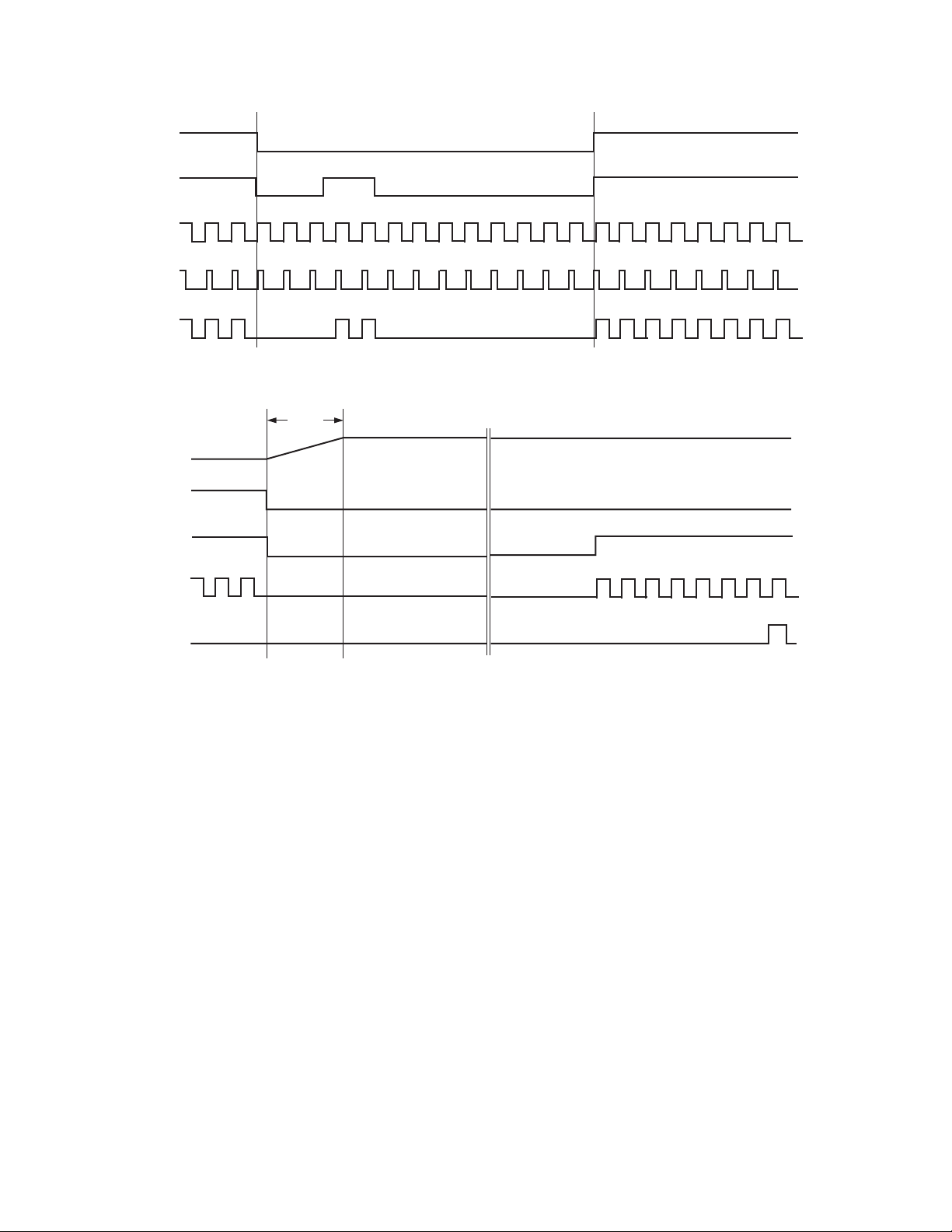
During slave mode operation, the SYNC/VGATE, Pin 45, is
configured as an input for an external VGATE signal. While
operating in this mode, the external VGATE signal can be used
to mask the V1–V4 and CLPOB outputs. There are two options
available for masking the V1–V4 and CLPOB outputs. The
selection is made by setting the MSHUT/VGATE_EN register
located at Control Addr 0x01. Examples of these two options
are shown in Figures 26 and 27.
VD
HD
VGATE
(PIN 45)
VGATE
(INTERNAL)
V1–V4
Figure 26 shows an example of MSHUT/VGATE_EN = 0. In
this example, the VGATE signal is internally latched on the
falling edge of HD, resulting in the V1–V4 and CLPOB outputs
being masked when the internally latched VGATE signal is High.
Figure 27 shows an example when MSHUT/VGATE_EN = 1.
In this example, the preprogrammed MSHUT signal blocks the
VGATE input from masking V1–V4 and CLPOB outputs while
MSHUT is Low. The internally latched VGATE signal will
only mask V1–V4 and CLPOB when MSHUT is High while
operating in this mode.
CLPOB
V1–V4 AND CLPOB MASKED
V1–V4 AND CLPOB MASKED
Figure 26. Example of VGATE Input Masking V1–V4 and CLPOB Outputs with MSHUT/VGATE_EN = 0
VD
HD
VGATE
(PIN 45)
VGATE
(INTERNAL)
MSHUT
V1–V4
CLPOB
V1–V4 AND CLPOB MASKED
REV. 0
Figure 27. Example of VGATE Input Masking V1–V4 and CLPOB Outputs with MSHUT/VGATE_EN = 1
–29–
Page 30

AD9898
VERTICAL TIMING GENERATION
The AD9898 provides a very flexible solution for generating
vertical CCD timing and can support multiple CCDs and different system architectures. The 4-phase vertical transfer clocks
V1–V4 are used to shift each line of pixels into the horizontal
output register of the CCD. The AD9898 vertical outputs can
be individually programmed into four different vertical pulse
patterns identified as VTP0, VTP1, VTP2, and VTP3. Each
vertical pulse pattern is a unique set of preconfigured V1–V4
sequences. Once the vertical patterns have been configured
using the registers in Table XVII, pointer registers are used to
select which region of the CCD a particular vertical pattern is
output in. The pointer registers are described in Table XV.
Up to five unique CCD regions may be specified. The readout
of the entire field is constructed by combining one or more of
the individual regions sequentially. With up to five region areas
available, different steps of the readout, such as high speed line
shifts and vertical image transfer, can be supported.
Creating Vertical Sequences
Figures 28, 29, and 30 provide an overview of how the vertical
timing is generated in four basic steps.
Step 1
Create the Individual Pulses for Patterns VTP0, VTP1, VTP2,
and VTP3 (See Figure 28)
The registers shown in Table XV are used to generate the
individual vertical timing pulses, as shown in Figure 28. The
VTPLENx determines the number of pixels between pulse
repetitions. The start polarity (VxSTARTPOLx) sets the starting polarity of the vertical sequence and can be programmed
high or low. The first toggle position (VxTOG1POSx) and
second toggle position (VxTOG2POSx) are the pixel locations
within the line where the pulse transitions.
Step 2
Create the Individual Vertical Sequences (See Figure 29)
The individual vertical sequences are created by assigning pulse
repetitions to patterns VTP0, VTP1, VTP2, and VTP3, using
VTPREPx registers in Table XVI. The number of repetitions
(VTPREPx) determines the number of pulse repetitions desired
within a single line. Programming 1 for VTPREPx gives a single
pulse, while setting it to 0 will provide a fixed dc output based
on the start polarity value. Figure 29 shows an example of a VTPx
sequence of two VTPx patterns made by setting VTPREPx = 2.
Step 3
Output Vertical Sequences into CCD Regions (See Figure 30)
The AD9898 arranges individual sequences into CCD regions
through the use of sequence pointers (VTPSEQPTRx) and
vertical transfer pattern select (VTPSELx) registers, as described
in Table XVI. The VTPSEQPTRx registers are used to point to
a desired VTPSELx register whose value determines what VTPx
pattern will be output on the V1–V4 pins. For example, if
VTPSEQPTR0 = 1 and VTPSEL1 = 2, the VTP2 pulse pattern
would output while operating in Region 0 of the CCD.
Step 4
Combining CCD Regions (See Figure 30)
The entire field readout can be built by combining multiple regions
by using mode registers SCP0, SCP1, SCP2, SCP3, and SCP4.
The individual CCD regions are combined into a complete field
readout using the sequence change position (SCPx) pointers as
described in Table XVII. Figure 30 shows how each field is
divided into multiple regions which allows the user to change
vertical timing during various stages of the image readout. The
boundaries of each region are defined by the sequence change
position (SCP). Each SCP is an 8-bit value representing the line
number boundary region. A total of four SCPs allow up to five
different regions in the field to be defined. The first SCP0 is
always hard coded to line zero, and the remaining four SCPs are
register programmable.
050100 150 200 250 300 350 400
HD
12 3
V1
V2
45 6
V3
V4
10 11 12
VTPLENx [8:0] = 210
PROGRAMMABLE CLOCK POSITIONS
1. V1STARTPOLx = 0
2. V1TOG1x[8:0] = 50
3. V1TOG2x[8:0] = 130
4. V2STARTPOLx = 1
5. V2TOG1x[8:0] = 30
6. V2TOG2x[8:0] = 150
7. V3STARTPOLx = 1
8. V3TOG1x[8:0] = 110
9. V3TOG2x[8:0] = 180
10. V4STARTPOLx = 0
11. V4TOG1x[8:0] = 20
12. V4TOG2x[8:0] = 160
897
Figure 28. Step 1: Create Individual Vertical Pulses for VTP0, VTP1, VTP2, and VTP3 Patterns
REV. 0–30–
Page 31
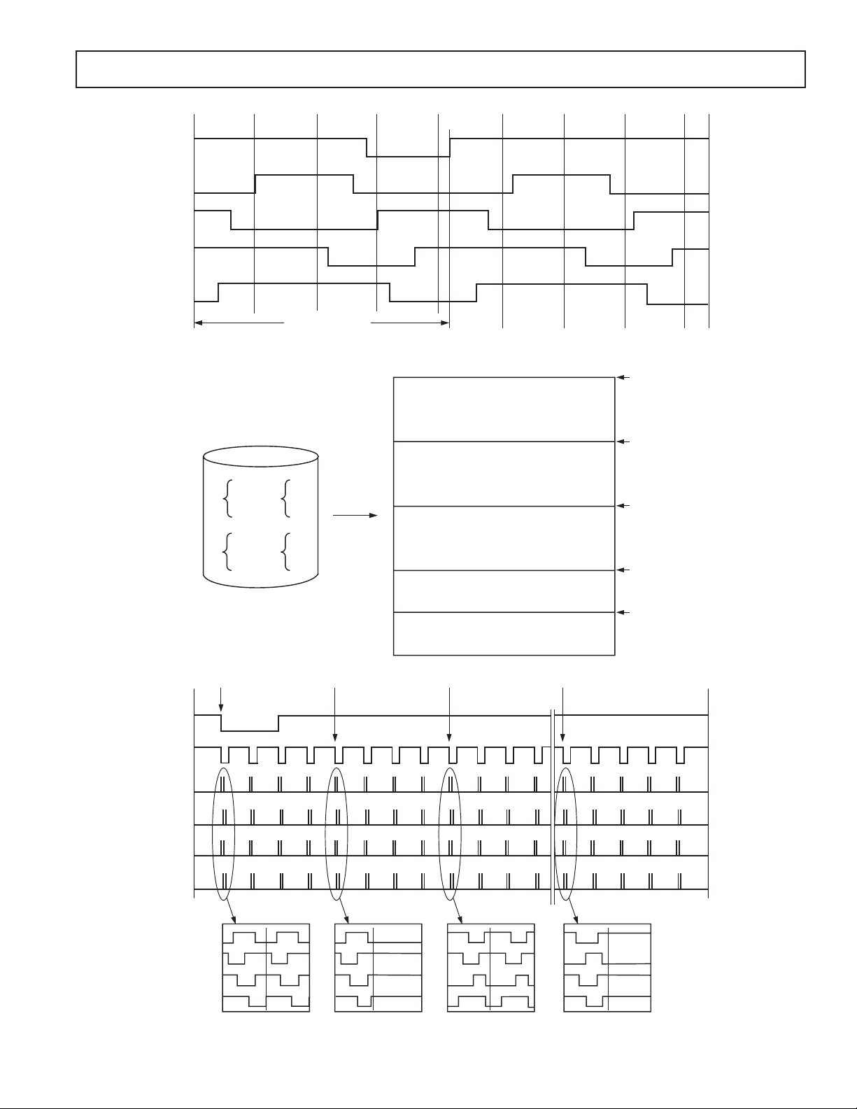
050 100 150 200 250 300 350 400
HD
12 3
V1
V2
45 6
AD9898
V3
V4
10 11 12
VTPLENx [8:0] = 210
897
Figure 29. Step 2: Create Individual Sequences for V1–V4 Outputs by Assigning Pulse Repetitions to VTP0, VTP1,
VTP2, and VTP3 Patterns. This Example Shows VTPREPx = 2.
SCP0
(FIXED AT LINE 0)
SCP1 [7:0]
SCP2 [7:0]
SCP3 [7:0]
SCP4 [7:0]
VERTICAL TRANSFER PULSES
VTP0
VTP2
V1
V2
VTP1
V3
V4
V1
V2
VTP3
V3
V4
V1
V2
V3
V4
V1
V2
V3
V4
CCD REGION0
CCD REGION1
CCD REGION2
CCD REGION3
CCD REGION4
VD
HD
SCP 0
REGION 0
(FIXED AT LINE 0)
V1
V2
V3
V4
VTP0
VTPREP0 = 2
SCP 1
REGION 1
(LINE 4)
VTP0
VTPREP0 = 1
SCP 2
REGION 2
(LINE 7)
VTP2
VTPREP2 = 2
SCP 4
REGION 4
(LINE (N + 7))
VTP1
VTPREP1 = 1
Figure 30. Steps 3 and 4: Example of Building an Entire Field Readout by Assigning Sequences to Multiple CCD Regions
REV. 0
–31–
Page 32

AD9898
Table XV. V1–V4 Registers to Configure V1–V4 Pulse for Each VTP Pattern
Register Bit Register Reference VTP
Name Width Type Counter Range Description Pattern
VTPLEN0 9 Sys_Reg(1) V Counter 0–511 Length between Repetitions
V1STARTPOL0 1 Sys_Reg(1) High/Low V1 Starting Polarity for VTP0 (0 = LO, 1 = HI)
V2STARTPOL0 1 Sys_Reg(1) High/Low V2 Starting Polarity for VTP0 (0 = LO, 1 = HI)
V3STARTPOL0 1 Sys_Reg(1) High/Low V3 Starting Polarity for VTP0 (0 = LO, 1 = HI)
V4STARTPOL0 1 Sys_Reg(1) High/Low V4 Starting Polarity for VTP0 (0 = LO, 1 = HI)
V1TOG1POS0 9 Sys_Reg(1) V Counter 0–511 V1 Toggle Position 1 for VTP0 V
V1TOG2POS0 9 Sys_Reg(1) V Counter 0–511 V1 Toggle Position 2 for VTP0 T
V2TOG1POS0 9 Sys_Reg(1 and 2) V Counter 0–511 V2 Toggle Position 1 for VTP0 P
V2TOG2POS0 9 Sys_Reg(2) V Counter 0–511 V2 Toggle Position 2 for VTP0 0
V3TOG1POS0 9 Sys_Reg(2) V Counter 0–511 V3 Toggle Position 1 for VTP0
V3TOG2POS0 9 Sys_Reg(2 and 3) V Counter 0–511 V3 Toggle Position 2 for VTP0
V4TOG1POS0 9 Sys_Reg(3) V Counter 0–511 V4 Toggle Position 1 for VTP0
V4TOG2POS0 9 Sys_Reg(3) V Counter 0–511 V4 Toggle Position 2 for VTP0
VTPLEN1 9 Sys_Reg(3) V Counter 0–512 Length between Repetitions
V1STARTPOL1 1 Sys_Reg(3) High/Low V1 Starting Polarity for VTP1 (0 = LO, 1 = HI)
V2STARTPOL1 1 Sys_Reg(3) High/Low V2 Starting Polarity for VTP1 (0 = LO, 1 = HI)
V3STARTPOL1 1 Sys_Reg(4) High/Low V3 Starting Polarity for VTP1 (0 = LO, 1 = HI)
V4STARTPOL1 1 Sys_Reg(4) High/Low V4 Starting Polarity for VTP1 (0 = LO, 1 = HI)
V1TOG1POS1 9 Sys_Reg(4) V Counter 0–511 V1 Toggle Position 1 for VTP1 V
V1TOG2POS1 9 Sys_Reg(4) V Counter 0–511 V1 Toggle Position 2 for VTP1 T
V2TOG1POS1 9 Sys_Reg(4) V Counter 0–511 V2 Toggle Position 1 for VTP1 P
V2TOG2POS1 9 Sys_Reg(4 and 5) V Counter 0–511 V2 Toggle Position 2 for VTP1 1
V3TOG1POS1 9 Sys_Reg(5) V Counter 0–511 V3 Toggle Position 1 for VTP1
V3TOG2POS1 9 Sys_Reg(5) V Counter 0–511 V3 Toggle Position 2 for VTP1
V4TOG1POS1 9 Sys_Reg(5 and 6) V Counter 0–511 V4 Toggle Position 1 for VTP1
V4TOG2POS1 9 Sys_Reg(6) V Counter 0–511 V4 Toggle Position 2 for VTP1
VTPLEN2 9 Sys_Reg(6) V Counter 0–512 Length between Repetitions
V1STARTPOL2 1 Sys_Reg(6) High/Low V1 Starting Polarity for VTP2 (0 = LO, 1 = HI)
V2STARTPOL2 1 Sys_Reg(6) High/Low V2 Starting Polarity for VTP2 (0 = LO, 1 = HI)
V3STARTPOL2 1 Sys_Reg(6) High/Low V3 Starting Polarity for VTP2 (0 = LO, 1 = HI)
V4STARTPOL2 1 Sys_Reg(6) High/Low V4 Starting Polarity for VTP2 (0 = LO, 1 = HI)
V1TOG1POS2 9 Sys_Reg(6) V Counter 0–511 V1 Toggle Position 1 for VTP2 V
V1TOG2POS2 9 Sys_Reg(7) V Counter 0–511 V1 Toggle Position 2 for VTP2 T
V2TOG1POS2 9 Sys_Reg(7) V Counter 0–511 V2 Toggle Position 1 for VTP2 P
V2TOG2POS2 9 Sys_Reg(7) V Counter 0–511 V2 Toggle Position 2 for VTP2 2
V3TOG1POS2 9 Sys_Reg(7 and 8) V Counter 0–511 V3 Toggle Position 1 for VTP2
V3TOG2POS2 9 Sys_Reg(8) V Counter 0–511 V3 Toggle Position 2 for VTP2
V4TOG1POS2 9 Sys_Reg(8) V Counter 0–511 V4 Toggle Position 1 for VTP2
V4TOG2POS2 9 Sys_Reg(8) V Counter 0–511 V4 Toggle Position 2 for VTP2
VTPLEN3 9 Sys_Reg(9) V Counter 0–512 Length between Repetitions
V1STARTPOL3 1 Sys_Reg(9) High/Low V1 Starting Polarity for VTP3 (0 = LO, 1 = HI)
V2STARTPOL3 1 Sys_Reg(9) High/Low V1 Starting Polarity for VTP3 (0 = LO, 1 = HI)
V3STARTPOL3 1 Sys_Reg(9) High/Low V1 Starting Polarity for VTP3 (0 = LO, 1 = HI)
V4STARTPOL3 1 Sys_Reg(9) High/Low V1 Starting Polarity for VTP3 (0 = LO, 1 = HI)
V1TOG1POS3 9 Sys_Reg(9) V Counter 0–511 V1 Toggle Position 1 for VTP3 V
V1TOG2POS3 9 Sys_Reg(9) V Counter 0–511 V1 Toggle Position 2 for VTP3 T
V2TOG1POS3 9 Sys_Reg(9 and 10) V Counter 0–511 V2 Toggle Position 1 for VTP3 P
V2TOG2POS3 9 Sys_Reg(10) V Counter 0–511 V2 Toggle Position 2 for VTP3 3
V3TOG1POS3 9 Sys_Reg(10) V Counter 0–511 V3 Toggle Position 1 for VTP3
V3TOG2POS3 9 Sys_Reg(10 and 11) V Counter 0–511 V3 Toggle Position 2 for VTP3
V4TOG1POS3 9 Sys_Reg(11) V Counter 0–511 V4 Toggle Position 1 for VTP3
V4TOG2POS3 9 Sys_Reg(11) V Counter 0–511 V4 Toggle Position 2 for VTP3
REV. 0–32–
Page 33

AD9898
Table XVI. Mode_A and Mode_B Registers for VTPx Selection
Register Bit Register
Name Width Type Range Description
VTPSEQPTR0* 3 Mode_Reg(2) Vertical Transfer Pulse Pointer Used in CCD Region 0
(0 = VTPSEL0, 1 = VTPSEL1, 2 = VTPSEL2, 3 = VTPSEL3
4 = VTPSEL0 for EVEN Line and VTPSEL1 for ODD Line
5 = VTPSEL2 for EVEN Line and VTPSEL3 for ODD Line)
VTPSEQPTR1* 3 Mode_Reg(2) Vertical Transfer Pulse Pointer Used in CCD Region 1
(0 = VTPSEL0, 1 = VTPSEL1, 2 = VTPSEL2, 3 = VTPSEL3
4 = VTPSEL0 for EVEN Line and VTPSEL1 for ODD Line
5 = VTPSEL2 for EVEN Line and VTPSEL3 for ODD Line)
VTPSEQPTR2* 3 Mode_Reg(2) Vertical Transfer Pulse Pointer Used in CCD Region 2
(0 = VTPSEL0, 1 = VTPSEL1, 2 = VTPSEL2, 3 = VTPSEL3
4 = VTPSEL0 for EVEN Line and VTPSEL1 for ODD Line
5 = VTPSEL2 for EVEN Line and VTPSEL3 for ODD Line)
VTPSEQPTR3* 3 Mode_Reg(2) Vertical Transfer Pulse Pointer Used in CCD Region 3
(0 = VTPSEL0, 1 = VTPSEL1, 2 = VTPSEL2, 3 = VTPSEL3
4 = VTPSEL0 for EVEN Line and VTPSEL1 for ODD Line
5 = VTPSEL2 for EVEN Line and VTPSEL3 for ODD Line)
VTPSEQPTR4* 3 Mode_Reg(2) Vertical Transfer Pulse Pointer Used in CCD Region 4
(0 = VTPSEL0, 1 = VTPSEL1, 2 = VTPSEL2, 3 = VTPSEL3
4 = VTPSEL0 for EVEN Line and VTPSEL1 for ODD Line
5 = VTPSEL2 for EVEN Line and VTPSEL3 for ODD Line)
VTPSEL0 2 Mode_Reg(3) (0 = VTP0, 1 = VTP1, 2 = VTP2, 3 = VTP3)
VTPSEL1 2 Mode_Reg(3) (0 = VTP0, 1 = VTP1, 2 = VTP2, 3 = VTP3)
VTPSEL2 2 Mode_Reg(3) (0 = VTP0, 1 = VTP1, 2 = VTP2, 3 = VTP3)
VTPSEL3 2 Mode_Reg(3) (0 = VTP0, 1 = VTP1, 2 = VTP2, 3 = VTP3)
VTPREP0 3 Mode_Reg(3) 0–7 Number of VTP0 Pulse Repetitions within a Line
VTPREP1 3 Mode_Reg(4) 0–7 Number of VTP1 Pulse Repetitions within a Line
VTPREP2 3 Mode_Reg(4) 0–7 Number of VTP2 Pulse Repetitions within a Line
VTPREP3 3 Mode_Reg(4) 0–7 Number of VTP3 Pulse Repetitions within a Line
*Registers 6 and 7 are not used.
Table XVII. Mode_A and Mode_B Registers for CCD Region Selection
Register Bit Register
Name Width Type Range Description
SCP1 8 Mode_Reg(2) 0–255 lines Sequence Change Position 1
SCP2 8 Mode_Reg(3) 0–255 lines Sequence Change Position 2
SCP3 8 Mode_Reg(3) 0–255 lines Sequence Change Position 3
SCP4 8 Mode_Reg(3) 0–255 lines Sequence Change Position 4
REV. 0
–33–
Page 34

AD9898
Special Vertical Sweep Mode Operation
The AD9898 contains a special mode of vertical timing operation
called sweep mode. This mode is used to generate a continuous number of repetitive vertical pulses that span multiple HD
lines. One example of when this mode may be needed is the
start of the CCD readout operation. At the end of the image
exposure, but before the image is transferred by the sensor gate
pulses, the vertical interline CCD registers should be cleared of
all charge. The charge can be shifted out quickly with a long
series of pulses on the V1–V4 outputs. This operation will span
multiple HD line lengths.
Table XVIII. Description of SVREP_MODE Register
SVREP_MODE Description of Sweep Mode Operation
00 Normal Vertical Timing Operation in All CCD Regions
01 Special Vertical Sweep Mode Timing Output in CCD Region0 Only
10 Special Vertical Sweep Mode Timing Output in CCD Region3 Only
11 Special Vertical Sweep Mode Timing Output in CCD Region0 and CCD Region3
HD
V1–V4
Normally the sequences are contained within one HD line length,
but with the sweep mode enabled, the HD boundaries will be
ignored until the region is finished. The special vertical sweep
mode operation is only output in CCD Region0 and CCD
Region3. (See Figures 33 and 34.) The SVREP_MODE register
located at control Address 0x0A is used to enable and configure
the special sweep mode operation as described in Table XVIII.
The maximum number of repeats in each region is 2048
while operating in this mode using the SVREP0 and SVREP3
Mode_Reg(4) registers.
Figure 31. NonOverlapping Example for Normal Vertical Timing Operation with SVREP_MODE = 0 and VTPREPx = 4
HD
V1–V4
NOT OUTPUT BECAUSE THE 8TH
REPETITION OVERLAPS WITH HD
Figure 32. Overlapping Example for Normal Vertical Timing Operation with SVREP_MODE = 0 and VTPREPx = 8
HD
V1–V4
SCP0
CCD REGION0
01 20
SCP1 = 3
Figure 33. Sweep Mode Timing Example with SVREP_MODE = 1 and SVREP0 = 28
HD
V1–V4
SCP3
CCD REGION3
01 20
SCP4 = 3
Figure 34. Sweep Mode Timing Example with SVREP_MODE = 2 and SVREP3 = 28
REV. 0–34–
Page 35

AD9898
Table XIX. HD and VD Registers
Register Bit Reference Range
Name Width Register Type Counter Pixels Description
SPAT_EN 1 Control (Addr 0x0A) SPAT Enable Control
(0 = SPAT Disabled, 1 = SPAT Enabled)
SPATLOGIC 4 Control (Addr 0x0A) SPAT Logic Setting
V1SPAT_TOG1 13 Mode_Reg(5) ST 0–8192 Polarity Change Position Start for V1 SPAT
V1SPAT_TOG2 13 Mode_Reg(5) ST 0–8192 Polarity Change Position End for V1 SPAT
V2SPAT_TOG1 13 Mode_Reg(6) ST 0–8192 Polarity Change Position Start for V2 SPAT
V2SPAT_TOG2 13 Mode_Reg(6) ST 0–8192 Polarity Change Position End for V2 SPAT
V3SPAT_TOG1 13 Mode_Reg(6 and 7) ST 0–8192 Polarity Change Position Start for V3 SPAT
V3SPAT_TOG2 13 Mode_Reg(7) ST 0–8192 Polarity Change Position End for V3 SPAT
V4SPAT_TOG1 13 Mode_Reg(7) ST 0–8192 Polarity Change Position Start for V4 SPAT
V4SPAT_TOG2 13 Mode_Reg(7 and 8) ST 0–8192 Polarity Change Position End for V4 SPAT
Special Vertical Timing (SPAT)
The AD9898 provides additional special vertical timing (SPAT)
generation, which is output in the same line as the VSG pulse.
The SPAT timing allows for configuring a second vertical output pulse in the VSG line. Tables XIX and XX list the registers
used to generate the SPAT timing.
Figures 35 and 36 show how the SPAT timing can be either an
AND case or an OR case, depending on the value set in the
SPATLOGIC register. As these figures show, the internal SPAT
timing for the AND case will start High and then go Low at the
first VxSPAT_TOG1 position. In the OR case, the internal
VD
HD
13-BIT
ST COUNTER
(FIXED)
INTERNAL V2
WITHOUT
SPAT APPLIED
INTERNAL SPAT
TIMING FOR V2 WITH
SPATLOGIC = 1
SPAT timing will initially start Low and then toggle High at the
first VxSPAT_TOG1 position. This provides the ability to
output the second vertical pulse when the internal Vx pulse is
in both High and Low states.
Table XX. SPATLOGIC Register (Addr 0x0A)
SPATLOGIC [3:0] Description
3210
V4 V3 V2 V1 0 = OR, 1 = AND
21
REV. 0
V2 OUTPUT WITH
SPAT APPLIED
VSGx
1. THE VxSPAT_TOG1 AND VxSPAT_TOG2 REGISTERS REFERENCE THE 13-BIT ST COUNTER.
2. THE INTERNAL SPAT TIMING IS APPLIED IN THE SAME LINE AS THE VSGx PULSE.
PROGRAMMABLE CLOCK POSITIONS
1. VxSPAT_TOG1 (PROGRAMMABLE AT MODE_REGs).
2. VxSPAT_TOG2 (PROGRAMMABLE AT MODE_REGs).
Figure 35. SPAT Example Applied to V2 with SPATLOGIC = xx1x
–35–
Page 36

AD9898
VD
HD
13-BIT
ST COUNTER
(FIXED)
INTERNAL V1
WITHOUT
SPAT APPLIED
INTERNAL SPAT
TIMING FOR V1 WITH
SPATLOGIC = 0
V1 OUTPUT WITH
SPAT APPLIED
VSGx
21
1. THE VxSPAT_TOG1 AND VxSPAT_TOG2 REGISTERS REFERENCE THE 13-BIT ST COUNTER.
2. THE INTERNAL SPAT TIMING IS APPLIED IN THE SAME LINE AS THE VSGx PULSE.
PROGRAMMABLE CLOCK POSITIONS
1. VxSPAT_TOG1 (PROGRAMMABLE AT MODE_REGs).
2. VxSPAT_TOG2 (PROGRAMMABLE AT MODE_REGs).
Figure 36. SPAT Example Applied to V1 with SPATLOGIC = xxx0
REV. 0–36–
Page 37

AD9898
Table XXI. SUBCK Registers
Bit Reference
Register Name Width Register Type Counter Range Description
SUBCKNUM 11 Control (Addr 0x0B) 0–2047 Pulses Number of SUBCK Pulses per Field
SUBCKSUPPRESS 1 Control (Addr 0x01) 0–1 Pulse Suppress First SUBCK after Last VSG
Line Pulse
SUBCK_EN 1 Control (Addr 0x0B) SUBCK Output Enable Control
(0 = Disable, 1 = Enable)
SUBCKMODE_HP 1 Control (Addr 0x01) High Speed Shutter Mode Operation
SUBCKNUM_HP 3 Control (Addr 0x0B) 0–7 Pulses High Speed Shutter SUBCLK
Position/Number
SUBCK1TOG1 9 System_Reg(14) OL-Counter 0–511 Pixel Location SUBCLK1 First Toggle Position
SUBCK1TOG2 9 System_Reg(14) OL-Counter 0–511 Pixel Location SUBCLK1 Second Toggle Position
SUBCK2TOG1 9 System_Reg(15) OL-Counter 0–511 Pixel Location SUBCLK2 First Toggle Position
SUBCK2TOG2 9 System_Reg(15) OL-Counter 0–511 Pixel Location SUBCLK2 Second Toggle Position
SUBCKSEL 1 Mode_Reg(2) (0 = SUBCK1, 1 = SUBCK2)
ELECTRONIC SHUTTER TIMING CONTROL
CCD image exposure time is controlled through the use of the
CCD substrate clock signal (SUBCK), which pulses the CCD
substrate to clear out accumulated charge prior to the exposure
period. The AD9898 supports three types of electronic shuttering: normal shutter mode, suppression shutter mode, and high
speed shutter mode. Table XXI contains the registers required
for programming SUBCK pulses for each of these modes.
Normal Shutter Mode
Figure 37 shows the VD and SUBCK output for normal shutter
mode. The SUBCK will pulse once per line. The number of
SUBCK pulses per field can be programmed by setting register
SUBCKNUM (Addr 0x0B). As shown in Figure 37, the SUBCK
pulses will always begin on the line after the sensor gate occurs,
specified by VSGACTLINE (Mode_Reg(1)).
SUBCK Suppression Mode
Normally the SUBCKs will begin to pulse on the line following
the last sensor gate line (VSG). With some CCDs, the first
SUBCK following the VSG line needs to be suppressed. The
SUBCKSUPPRESS register allows for this suppression. The
first SUBCK following the last VSG pulse is suppressed when
SUBCKSUPPRESS = 1, as shown in Figure 38.
High Precision Shutter Mode
The high speed shutter mode can be operated in two different modes, single pulse and multiple pulse. These modes are
set up by programming the SUBCKNUM_HP register and
SUBCKMODE_HP register, as described in Table XXII and
shown in Figures 40 and 41.
Single Pulse Mode
In addition to the normal operating SUBCK pulse, one additional SUBCK pulse can be applied within the HD line while
operating in this mode. As shown in Figure 37, the location
of the additional SUBCK pulse is adjusted by setting the
SUBCKNUM_HP register as described in Table XXII. Finer
resolution of the exposure time is possible using this mode by
adding a SUBCK pulse in the line, as shown in Figure 40.
Multiple Pulse Mode
In addition to the normal operating SUBCK pulse, up to seven
sequential SUBCK pulses can be applied within the same line
while operating in this mode. As shown in Figure 41, the
number of additional SUBCK pulses is selectable by setting
SUBCKMODE_HP = 1 and the SUBCKNUM_HP registers
as described in Table XXII.
Table XXII. Single and Multiple Pulse Mode
SUBCKMODE_HP
01
Single Pulse Multiple Pulse
SUBCKNUM_HP Mode Mode
0Normal Shutter Normal Shutter
Mode Operation Mode Operation
1 Position No. 1 1 Additional Pulse
2 Position No. 2 2 Additional Pulses
3 Position No. 3 3 Additional Pulses
4 Position No. 4 4 Additional Pulses
5 Position No. 5 5 Additional Pulses
6 Position No. 6 6 Additional Pulses
7 Position No. 7 7 Additional Pulses
REV. 0
–37–
Page 38

AD9898
VD
HD
VSG1–
VSG2
SUBCK
1
SUBCK PROGRAMMABLE SETTINGS
1. SUBCK STARTING POLARITY IS ALWAYS HIGH.
2. FALLING EDGE OF SUBCK IS SET USING THE SUBCK1TOG1 OR SUBCK2TOG1 REGISTERS.
3. RISING EDGE OF SUBCK IS SET USING THE SUBCK1TOG2 OR SUBCK2TOG2 REGISTERS.
NUMBER OF SUBCK PULSES WITHIN THE FIELD IS SET USING THE SUBCKNUM REGISTER. IN THIS EXAMPLE, SUBCKNUM = 2.
23
t
EXP
t
EXP
Figure 37. Normal Shutter Mode
VD
HD
VSG1–
VSG2
SUBCK
1
SUBCK PROGRAMMABLE SETTINGS
SETTING SUBCKSUPPRESS REGISTER = 1 SUPPRESSES THIS FIRST SUBCK FOLLOWING VSG PULSE.
t
EXP
t
EXP
Figure 38. SUBCK Suppression Mode
REV. 0–38–
Page 39

HD
OLEN
9-BIT
OL-COUNTER
SUBCK
123456 7
NORMAL SHUTTER MODE PULSE
ALWAYS OUTPUT
Figure 39. Electronic Shutter Timing
HD
9-BIT
OL-COUNTER
SUBCK
1
Figure 40. Electronic Shutter Timing Example with SUBCKMODE_HP = 0 and SUBCKNUM_HP = 1
AD9898
HD
9-BIT
OL-COUNTER
SUBCK
123
Figure 41. Electronic Shutter Timing Example with SUBCKMODE_HP = 1 and SUBCKNUM_HP = 3
REV. 0
–39–
Page 40

AD9898
VSG TIMING
The VSG timing is controlled using the registers in Table XXIII.
Two unique preprogrammed VSG pulses can be configured
using the VSGTOG1_x (x = 0, 1) registers. As shown in
Figure 42, the period of the VSG pulse is set by programming
the VSGLEN register. The VSGSELx (x = 0, 1) can then be
Figure 42 also shows an example of the VSG pulse being output
in the fourth line by setting the VSGACTLINE = 3. The VSG1
and VSG2 pulses reference the 13-bit fixed ST counter, which
starts counting from the line set in the VSGACTLINE register.
The 13-bit counter allows for overlapping of the VSG pulse into
the next line, if needed.
used to point to either the VSGTOG1_0 or VSGTOG1_1 pulse.
Table XXIII. VSG Registers
Register Bit Reference
Name Width Register Type Counter Range Description
VSGMASK 6 Control (Addr 0x0A) VSG Mask Control
(00 = VSG1 masked, VSG2 masked)
(02 = VSG1 not masked, VSG2 masked)
(08 = VSG1 masked, VSG2 not masked)
(0A = VSG1 not masked, VSG2 not masked)
VSG_EN 1 Control (Addr 0x0B) High/Low VSG Output Enable Control
(0 = Disable VSG Outputs,
1 = Enable VSG Outputs)
VSGTOG1_0 11 Sys_Reg(13) ST 0–8191 Pixels VSG Sequence 1, Toggle Position 1
VSGTOG1_1 11 Sys_Reg(13) ST 0–8191 Pixels VSG Sequence 2, Toggle Position 1
VSGLEN 8 Sys_Reg(14) ST 0–255 Pixels VSG Pulsewidth
VSGSEL0 1 Mode_Reg(1) High/Low VSG1 Output Selector
(0 = VSGTOG1_0 applied on VSG1 output,
1 = VSGTOG1_1 applied on VSG1 output)
VSGSEL1 1 Mode_Reg(1) High/Low VSG2 Output Selector
(0 = VSGTOG1_0 applied on VSG2 output,
1 = VSGTOG1_1 applied on VSG2 output)
VSGACTLINE 7 Mode_Reg(1) 0–128 Lines VSG Active Line
VD
HD
13-BIT
ST COUNTER
(FIXED)
VSGx
1230
VSGACTLINE
1. VSGTOG1_x (x = 0, 1) REFERENCES THE 13-BIT ST COUNTER.
2. VSGACTLINE (PROGRAMMABLE AT MODE_REG (1)).
3. VSGLEN (PROGRAMMABLE AT SYS_REG (14)).
PROGRAMMABLE CLOCK POSITION
VSGTOG1_x (PROGRAMMABLE AT SYS_REG (13)).
Figure 42. Example of VSG Pulse
VSGLEN
1
REV. 0–40–
Page 41

AD9898
VSUB CONTROL
The CCD readout bias (VSUB) can be programmed to accommodate different CCDs. VSUB ON and OFF toggle positions
and polarity are controlled using VSUBTOG (Addr 0x0D) and
VSUBPOL (Addr 0x0D) registers, respectively, as described in
Table XXIV. Since the VSUBTOG is an 11-bit register, the
VSUB ON position is programmable within any line. Figure 43
shows an example of controlling VSUB using these registers.
Table XXIV. VSUB Registers
Register Bit Register Range
Name Width Type (Lines) Description
VSUBPOL 1 Control (0 = Low, 1 = High)
VSUBTOG 11 Control 0–2048 VSUB Toggle Position
SERIAL
WRITES
VSUB
1
2
VD
HD
3
VSUB Placement and Polarity
Figure 43 shows the sequence of events for programming the
VSUB ON and OFF toggle positions and polarity.
1. Program VSUBTOG = 2 and VSUBPOL = 1.
2. Since VSUBTOG and VSUBPOL are VD synchronous type
registers, the falling edge of VD will update the serial writes
from Step 1 here.
3. VSUB will be asserted high after two HD cycles.
4. Program VSUBTOG = 3 and VSUBPOL = 0.
5. Since VSUBTOG and VSUBPOL are VD synchronous type
registers, the falling edge of VD will update the serial writes
from Step 4 here.
6. VSUB will be asserted low after three HD cycles.
4
5
6
3 LINES2 LINES
Figure 43. VSUB Timing Example
REV. 0
–41–
Page 42

AD9898
MSHUT CONTROL
MSHUT Basic Operation
The AD9898 provides an MSHUT output pulse that can be
configured to control the mechanical shutter of the camera.
The registers used to control the MSHUT pulse are listed in
Table XXV.
The MSHUT pulse can be placed at the start of any line by using
the 11-bit MSHUTPOS register. The MSHUT pulsewidth is
The AD9898 offers four preprogrammed MSHUT patterns that
are selectable using the MSHUTPAT register. The
preprogrammed length is the same for all patterns set by the
MSHUTLEN register, but the active ON period of the
MSHUT pulse is different for each pattern, as shown in Figure
44. Figure 45 shows an example of selecting MSHUTPAT0
positioned to start three lines after the falling edge of VD with
MSHUTLEN = 5.
controlled using the MSHUTLEN register.
Table XXV. MSHUT and STROBE Registers
Register Name Bit Width Register Type Description
MSHUTPAT 2 Control (Addr 0x01) Selects MSHUT Pattern (See Figure 44)
(0 = MSHUTPAT0, 1 = MSHUTPAT1, 2 = MSHUTPAT2,
3 = MSHUTPAT3)
MSHUTINIT 1 Control (Addr 0x0C) MSHUT Initialize
(1 = MSHUT Output Held LOW, 0 = Normal Operation Resumes)
MSHUTEN 1 Control (Addr 0x0C) MSHUT Control (0 = MSHUT Held at Last State,
1 = MSHUT Output Enabled for Normal Operation)
MSHUTPOS 11 Control (Addr 0x0C) MSHUT Position during Normal Operation
MSHUTPOS_HP 3 Control (Addr 0x0C) MSHUT Position during High Precision Operation
MSHUTLEN 8 Sys_Reg(13) MSHUT Pattern Length (See Figures 44 and 45)
STROBE_EN 1 Control (Addr 0x0B) STROBE Output Enable Control
(0 = STROBE Output Held Low, 1 = Enable STROBE Output)
HD
MSHUTPAT0
MSHUTPAT1
MSHUTPAT2
MSHUTPAT3
VD
HD
VSG1–
VSG2
SUBCK
MSHUT
MSHUTLEN + 1
Figure 44. MSHUT Patterns Available by Setting MSHUTPAT Register
123123 546
t
EXP
MSHUTPOS = 3 MSHUTPAT = 0, MSHUTLEN = 5
Figure 45. Example of MSHUT Timing with MSHUTEN = 1 and MSHUTPOS_HP = 0
REV. 0–42–
Page 43

AD9898
MSHUT High Precision Operation
The MSHUTPOS_HP register allows more precise control of
the MSHUT position within a line. Under normal MSHUT
operation when MSHUTPOS_HP = 0, the MSHUT polarity
changes from high to low on the negative edge of the HD pulse,
as shown in Figure 44. By using the MSHUTPOS_HP register,
the rising and falling edges of MSHUT can be delayed by multiples of the OL counter length, which has been set in the OLEN
VD
HD
VSG1–
VSG2
SUBCK
MSHUT
12312 3 546
OL
COUNTER
MSHUTPOS = 3
OL
COUNTEROLCOUNTER
MSHUTPAT = 0, MSHUTLEN = 5
COUNTER
Figure 46. Example of MSHUT High Precision Timing—MSHUTEN = 1 and MSHUTPOS_HP = 3
VD
register. For example, if MSHUTPOS_HP = 3, the MSHUT
rising and falling edges will be delayed by three OL counter
cycles after the falling edge of HD, as shown in Figure 46.
Figure 46 provides an example of high precision MSHUT and
SUBCK timing. In this example, the length of the OL counter
is shorter. This provides very precise control of the placement
of the MSHUT pulse within a line.
t
EXP
OL
12312 3 546
t
EXP
DELAY = 3 OL
COUNTER LENGTHS
MSHUTPOS = 3
MSHUT OUTPUT IN NORMAL OPERATION WITH MSHUTPOS_HP = 0
MSHUT OUTPUT IN HIGH PRECISION OPERATION WITH MSHUTPOS_HP = 3
MSHUTPAT = 0, MSHUTLEN = 5
VSG1–
VSG2
SUBCK
MSHUT
MSHUT
HD
1
2
NOTES
1
2
Figure 47. Example of MSHUT High Precision Timing—MSHUTEN = 1, MSHUTPOS_HP = 3, with
SUBCKMODE_HP = 1, SUBCKNUM_HP = 3
REV. 0
–43–
Page 44
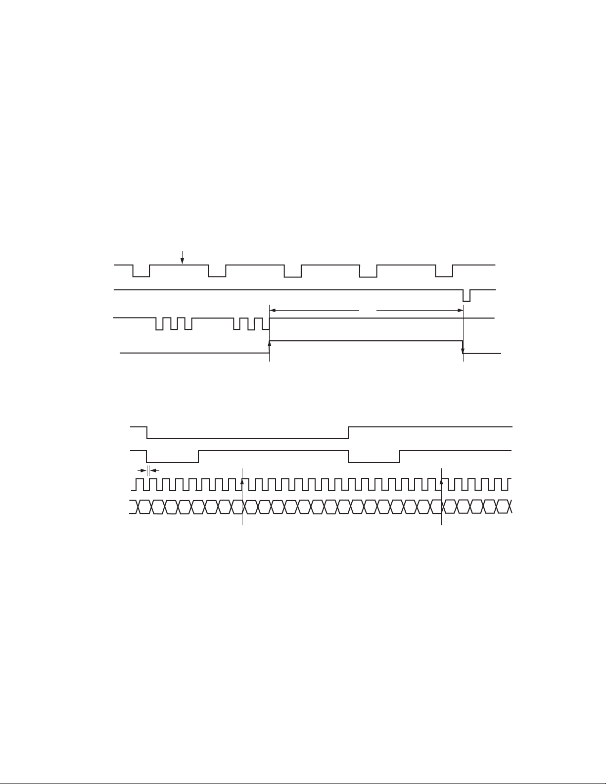
AD9898
STROBE Control
The AD9898 provides a STROBE output pulse that can be used
to trigger the camera flash circuit. STROBE operation is set by
only one register, as described in Table XXV. The STROBE
output is held Low when STROBE_EN (Addr 0x0B) is set to
0 and enabled when set to 1. Providing STROBE_EN = 1, the
STROBE output pulse will be asserted High on the rising edge of
the last SUBCK pulse in the field, as shown in Figure 48.
Figure 48 also shows the STROBE pulse asserted Low again on
the rising edge of VSG.
SLAVE AND MASTER MODE OPERATION
The AD9898 can be operated in either slave mode or master
mode. It defaults to the slave mode operation at power-up. The
SET STROBE_EN (ADDR 0x0B) = 1
VD
VSG1–
VSG2
SUBCK
STROBE
1
SLAVE_MODE register (Addr 0xD6) can be used to configure
the AD9898 into master mode by setting SLAVE_MODE = 0.
Slave Mode Operation
While operating in slave mode, VD, HD, and VGATE are provided externally from the image processor. VGATE is input
active high on Pin 45. Unlike master mode operation, there is a
7 CLI clock cycle delay from the falling edge of HD to when the
12-bit gray code H counter is reset to zero (see Figure 49).
Master Mode Operation
While operating in master mode, VD and HD are outputs and
the SYNC/VGATE pin is configured as an external SYNC input.
Master mode is selected by setting register SLAVE_MODE
(Addr 0xD6) = 0.
t
EXP
2
1. STROBE OUTPUT ASSERTED HIGH ON RISING EDGE OF LAST SUBCK PULSE.
2. STROBE OUTPUT ASSERTED LOW ON NEGATIVE EDGE OF VSG PULSE.
Figure 48. STROBE Output Timing
VD
HD
CLI
H-GRAY CODE
COUNTER
(PIXEL COUNTER)
H-COUNTER
3ns MIN
X XXXXXXXX 01 23 4567 89101112131401234
INTERNAL 12-BIT H-GRAY CODE COUNTER IS RESET 7 CLOCK CYCLES AFTER THE HD FALLING EDGE.
RESET
H-COUNTER
RESET
Figure 49. External VD/HD and Internal 12-Bit H-Gray Code Counter Synchronization, SLAVE Mode
REV. 0–44–
Page 45
AD9898
3
VARIABLE GAIN AMPLIFIER
The VGA provides a gain range of 6 dB to 40 dB, programmable
with 10-bit resolution through the serial digital interface. The
minimum gain of 6 dB is needed to match a 1 V input signal
with the ADC full-scale range of 2 V.
The VGA gain curve follows a linear-in-dB characteristic. The
exact VGA gain can be calculated for any gain register value
using the equation
Gain Code=×
()
+0 035 5 3..
where the code range is 0 to 1023. Figure 50 shows a typical
AD9898 VGA gain curve.
42
36
30
24
VGA GAIN (dB)
18
12
6
0 127
255 383 511 639 767 895 102
VGA GAIN REGISTER CODE
Figure 50. VGA Gain Curve
Optical Black Clamp
The optical black clamp loop is used to remove residual offsets
in the signal chain and to track low frequency variations in the
CCD’s black level. During the optical black (shielded) pixel
interval on each line, the ADC output is compared with a fixed
black level reference, selected by the user in the clamp level
register. Any value between 0 LSB and 63 LSB may be programmed with 6-bit resolution. The resulting error signal is
filtered to reduce noise, and the correction value is applied to
the ADC input through a D/A converter. Normally the optical
black clamp loop is turned on once per horizontal line, but this
loop can be updated more slowly to suit a particular application.
The optical black clamp is controlled by the CLPOB signal,
which is fully programmable (see Horizontal Clamping and
Blanking section). System timing examples are shown in the
Horizontal Timing Sequence Example section. The CLPOB
pulse should be placed during the CCD’s optical black pixel.
It is recommended that the CLPOB pulse duration be at least
20 pixels wide. Shorter pulsewidths may be used, but the ability
to track low frequency variations in the black level will be reduced.
A/D Converter
The AD9898 uses a high performance 10-bit ADC architecture,
optimized for high speed and low power. Differential nonlinearity
(DNL) performance is typically better than 0.5 LSB. The ADC
uses a 2 V input range. Better noise performance results from
using a larger ADC full-scale range.
Digital I/O States for Different Operating Conditions
Table XXVI describes the state of the digital I/Os for different
operating conditions.
Table XXVI. I/O Levels
I/O OCONT_REG1= 0 SW_RESET DIGSTBY SYNC
DCLK1 ACTIVE ACTIVE L ACTIVE
DCLK2 ACTIVE ACTIVE L ACTIVE
VD
HD
2
2
HHHH
HHHH
RG L L L ACTIVE
H1 H H H ACTIVE
H2 L L L ACTIVE
V1 H L H FREEZE
V2 H L L FREEZE
V3 H L L FREEZE
V4 H H H FREEZE
SUBCK H H H FREEZE
VSG1 H L H FREEZE
VSG2 H H H FREEZE
STROBE L L L FREEZE
MSHUT L L L FREEZE
FD H L L FREEZE
NOTES
1
OUTCONT_REG is a register setting located at Addr 0x05. It defaults to 0 at power-up.
2
VD and HD operating in master mode.
REV. 0
–45–
Page 46
AD9898
VDD
(INPUT)
1
CLI
(INPUT)
OUTCONT
(INTERNAL
SIGNAL)
SERIAL
WRITES
VD
(OUTPUT)
HD
(OUTPUT)
DIGITAL
OUTPUTS
DCLK2
(OUTPUT)
2
1
t
PWR
H1, V1, V2, V3, VSG1, VSG2, VSUB, SUBCK, FD
H2, RG, MSHUT, STROBE
2
4567
89 10
1V
ODD FIELD EVEN FIELD
1H
3
t
DELAY
ODD FIELD
DCLK1
(OUTPUT)
4
t
SETTLING
NOTES
1
OUTCONT IS AN INTERNAL SIGNAL CONTROLLED USING REGISTER OUTCONT_REG (ADDR 0x05).
2
DCLK2 WILL BE OUTPUT ON FD/DLCK2, PIN 16, PROVIDING REGISTER DCLK2SEL (ADDR 0xD5) = 1.
3
IT TAKES 11 CLI CLOCKS FROM WHEN OUTCONT GOES HIGH UNTIL VD, HD, AND DIGITAL OUTPUT DATA IS VALID.
4
THERE IS 500 s SETTLING TIME FROM WHEN THE DIGSTBY REGISTER IS SET TO WHEN THE DLCK1 IS STABLE.
Figure 51. Recommended Power-Up Sequence and Synchronization, Master Mode
POWER-UP
Recommended Power-Up Sequence for Master Mode
When the AD9898 is powered up, the following sequence is
recommended. (Refer to Figure 51 for each step.)
1. Turn on power supplies for AD9898.
2. Apply the CLI master clock input. CLI will be output on
DCLK2 (Pin 16) at this time.
3. Reset the internal AD9898 registers. Write a 0x000000 to
the SW_RESET register (Addr 0x00). This will set all
internal register values to their default values. (This step is
optional because an internal power-on reset circuit is
applied at power-up.)
4. Program the DIGSTBY and AFESTBY registers
(Addr 0x05) = 1, and program all other necessary control
registers.
5. Program system registers (Addr 0x14).
6. Program Mode_A registers (Addr 0x15).
7. Program Mode_B registers (Addr 0x16).
8. Program OUTCONT_REG register (addr 0x05) = 1.
(The internal OUTCONT signal will be asserted high at
this time and will enable the digital outputs.)
9. Program control register MODE (Addr 0x0A) = 0. This
selects Mode_A operation. (This step is optional because
the AD9898 defaults to Mode_A at initial power-up.)
10. Program control register MODE (Addr 0x0A) = 1. This
selects Mode_B operation. Complete this write at least
four CLI cycles before start of the next field.
REV. 0–46–
Page 47
VDD
(INPUT)
CLI
(INPUT)
OUTCONT
(INTERNAL
SIGNAL)
AD9898
SERIAL
WRITES
VD
(OUTPUT)
HD
(OUTPUT)
DIGITAL
OUTPUTS
DCLK1
AND
DCLK2
AFESTBY
(REGISTER)
DIGSTBY
(REGISTER)
156
1
NOTES
1
DCLK2 WILL BE OUTPUT ON FD/DLCK2, PIN 16, PROVIDING REGISTER DCLK2SEL (ADDR 0xD5) = 1.
2
IT TAKES 11 CLI CLOCKS FROM WHEN OUTCONT GOES HIGH UNTIL VD, HD, AND DIGITAL OUTPUT DATA IS VALID.
2
3
H1, V1, VSG1, VSG2, VSUB, SUBCK
H2, V2, V3, FD, RG, MSHUT, STROBE
Figure 52. Recommended Standby Sequence
t
DELAY
2
STANDBY MODE OPERATION
Recommended Standby Mode Sequence
When the AD9898 is going into standby operation, the following
sequence is recommended. (Refer to Figure 52 for each step.)
1. Program OUTCONT_REG (Addr 0x05) = 0. This will
assert the internal OUTCONT signal LO causing all digital
outputs to become disabled.
2. Program registers AFESTBY (Addr 0x05) = 0 and DIGSTBY
(Addr 0x05) = 0. The AD9898 is then in standby operation.
REV. 0
–47–
3. When it is time to come out of standby operation, program
register DIGSTBY (Addr 0x05) = 1 and register AFESTBY
(Addr 0x05) = 1.
4. Program necessary control registers.
5. Program control register MODE (Addr 0x0A) = 0. This
selects Mode_A operation.
6. Program register OUTCONT_REG (Addr 0x05) = 1. This
will assert the internal OUTCONT signal high, causing all
digital outputs to become active.
Page 48

AD9898
VDD
(INPUT)
CLI
(INPUT)
OUTCONT
(INTERNAL)
SERIAL
WRITES
VD
(OUTPUT)
HD
(OUTPUT)
DIGITAL
OUTPUTS
ODD FIELD EVEN FIELD
ODD FIELD
4
H1, V1, V2, V3, V4, VSG1, VSG2, VSUB, FD, SUBCK
H2, RG, MSHUT, STROBE
,
DCLK 1
DCLK 2*
AFESTBY
(REGISTER)
DIGSTBY
(REGISTER)
*DCLK2 WILL BE OUTPUT ON FD/DLCK2, PIN 16, PROVIDING REGISTER DCLK2SEL (ADDR 0xD5) = 1.
Figure 53. Recommended Power-Down Sequence
POWER-DOWN MODE OPERATION
Recommended Power-Down Sequence
When the AD9898 is going to be powered down, the following
sequence is recommended. (Refer to Figure 53 for each step.)
1. Program OUTCONT_REG (Addr 0x05) = 0.
2. Program registers AFESTBY (Addr 0x05) = 0 and DIGSTBY
(Addr 0x05) = 0.
3. Remove power from the AD9898.
REV. 0–48–
Page 49

AD9898
HORIZONTAL TIMING SEQUENCE EXAMPLE
Figure 54 shows a sample CCD layout. The horizontal register
contains 28 dummy pixels, which will occur on each line clocked
from the CCD. In the vertical direction, there are 10 optical
black (OB) lines at the front of the readout and two at the back.
The horizontal direction has four OB pixels in the front and 48
in the back.
To configure the AD9898 horizontal signals for this CCD, three
sequences can be used. Figure 55 shows the first sequence to be
used during vertical blanking. During this time, there are no
V
4 OB PIXELS 48 OB PIXELS
EFFECTIVE IMAGE AREA
H
HORIZONTAL CCD REGISTER
valid OB pixels from the sensor, so the CLPOB is not used. In
some cases, if the horizontal clocks are used during this time,
the CLPOB signal may be used to keep the AD9898’s clamp
partially settled.
Figure 56 shows the recommended sequence for the vertical OB
interval. The clamp signal is used across the whole line in order
to stabilize the clamp loop of the AD9898. Figure 57 shows the
recommended sequence for the effective pixel readout. The 48 OB
pixels at the end of each line are used for the CLPOB signal.
SEQUENCE 2 (OPTIONAL)
2 VERTICAL OB LINES
USE SEQUENCE 3
10 VERTICAL OB LINES
USE SEQUENCE 2
28 DUMMY PIXELS
Figure 54. Sample CCD Configuration
SEQUENCE 1: VERTICAL BLANKING
INVALID PIX VERTICAL SHIFT DUMMY INVALID PIXELS VERT SHIFT
CDIN
SHP
SHD
H1
H2
HD
CLPOB
CLPOB PULSE MAY BE USED DURING HORIZONTAL DUMMY PIXELS
IF THE H-CLOCKS ARE USED DURING VERTICAL BLANKING.
Figure 55. Horizontal Sequence during Vertical Blanking
REV. 0
–49–
Page 50

AD9898
SEQUENCE 2: VERTICAL OPTICAL BLACK LINES
CCDIN
SHP
SHD
H1
H2
HD
CLPOB
OPTICAL BLACK VER TICAL SHIFT DUMMY OPTICAL BLACK VERT SHIFT
Figure 56. Horizontal Sequence during Vertical Optical Black Pixels
SEQUENCE 3: EFFECTIVE PIXEL LINES
OPTICAL BLACK VERTICAL SHIFT DUMMY
CCDIN
SHP
SHD
H1
H2
HD
CLPOB
Figure 57. Horizontal Sequences during Effective Pixels
OB
EFFECTIVE PIXELS OPTICAL BLACK VERT SHIFT
REV. 0–50–
Page 51

AD9898
CIRCUIT LAYOUT INFORMATION
The AD9898 typical circuit connection is shown in Figure 58.
The PCB layout is critical to achieving good image quality from
the AD9898. All of the supply pins, particularly the AVDD,
TCVDD, RGVDD, and HVDD supplies, must be decoupled to
ground with good quality high frequency chip capacitors. The
decoupling capacitors should be located as close as possible to
the supply pins and should have a very low impedance path to a
continuous ground plane. There should also be a 4.7 µF or
larger value bypass capacitor for each main supply—AVDD,
RGVDD, HVDD, and DRVDD—although this is not necessary
for each individual pin. For most applications, it is easier to
share the supply for RGVDD and HVDD, which may be done
as long as the individual supply pins are separately bypassed. A
separate 3 V supply may also be used for DRVDD, but this
3V
ANALOG
EXTERNAL SYNC FROM ASIC/DSP
VSUB TO CCD
OUTCONT
SUPPLY
0.1F
3V
DRIVER
SUPPLY
10k
supply pin should still be decoupled to the same ground plane
as the rest of the chip. A separate ground for DRVSS is not
recommended.
The analog bypass pins (REFB, REFT) also should be carefully
decoupled to ground as close as possible to their respective pins.
The analog input (CCDIN) capacitor also should be located
close to the pin.
The H1, H2, and RG traces should be designed to have low
inductance to avoid excessive distortion of the signals. Heavier
traces are recommended because of the CCD’s large transient
current demand on H1 and H2. When possible, physically
locating the AD9898 closer to the CCD will reduce the inductance on these lines. As always, the routing path should be as
direct as possible from the AD9898 to the CCD.
V1–V4
7
VSG1, VSG2
SUBCK
TO V-DRIVER
3V
4.7F
DRIVER
SUPPLY
TO MECHANICAL SHUTTER CIRCUIT
0.1F
10
DATA
OUTPUTS
DCLK1, FD/DCLK2, HD, VD
TO STROBE CIRCUIT
DVDD
STROBE
FD/DCLK2
OUTCONT
AD9898
TOP VIEW
(Not to Scale)
VD
HD
HVDD
3V
HVSS
0.1F
38 37
36
35
34
33
32
31
30
29
28
27
26
25
23 24
H1
H2
RG
RGVSS
3
D0
1
D1
2
D2
3
D3
4
D4
5
DRVSS
6
DRVDD
7
D5
8
D6
9
D7
10
D8
11
D9
12
4
ANALOG SUPPLY
SUBCK
DVSS
48 47 46 45 44 43 42 41 40 39
PIN 1
IDENTIFIER
13 14 15 16 17 18 19 20 21 22
DCLK1
MSHUT
V1
V2
V3
V4
VSG1
VSG2
SYNC/VGATE
VSUB
Figure 58. Typical Circuit Configuration
SCK
SL
SDATA
REFB
REFT
AVSS
CCDIN
AVDD
CLI
TCVDD
TCVSS
RGVDD
H2, H1, RG
1.0F
1.0F
0.1F
0.1F
3
0.1F
INPUT CLOCK
4.7F
SERIAL
INTERFACE
CCD SIGNAL
0.1F
3V
ANALOG SUPPLY
3V
ANALOG SUPPLY
REV. 0
–51–
Page 52

AD9898
OUTLINE DIMENSIONS
48-Lead Lead Frame Chip Scale Package [LFCSP]
(CP-48)
Dimensions shown in millimeters
1.00
0.90
0.80
0.20
REF
12 MAX
SEATING
PLANE
BSC SQ
PIN 1
INDICATOR
TOP
VIEW
7.00
0.60 MAX
6.75
BSC SQ
0.50
0.40
0.30
1.00 MAX
0.65 NOM
0.05 MAX
0.02 NOM
0.50 BSC
COMPLIANT TO JEDEC STANDARDS MO-220-VKKD-2
COPLANARITY
0.08
37
36
25
24
0.60 MAX
BOTTOM
VIEW
5.50
REF
0.30
0.23
0.18
PIN 1
48
INDICATOR
1
C02877–0–5/03(0)
5.25
SQ
5.10
4.95
12
13
0.25 MIN
–52–
REV. 0
 Loading...