

Page 1
High Performance
www.BDTIC.com/ADI
FEATURES
HDMI/DVI transmitter compatible with HDMI 1.1 and
HDCP 1.1
Single 1.8 V power supply
Video/audio inputs are 3.3 V tolerant
80-lead, Pb-free LQFP
Digital video
80 MHz operation supports all video formats from 480i to
1080i and 720p
Programmable 2-way color space converter
Supports RGB, YCbCr, DDR, ITU656 formats
Auto input video format detection
Digital audio
Supports standard S/PDIF for stereo or compressed audio
up to 192 kHz
8-channel LPCM I2S audio up to 192 kHz
Special features for easy system design
On-chip MPU to perform HDCP operations
On-chip I
5 V tolerant I
No audio master clock needed for S/PDIF support
2
C master to handle EDID reading
2
C and MPD I/Os, no extra device needed
CLK
VSYNC
HSYNC
D[23:0]
S/PDIF
MCLK
I2S[3:0]
DE
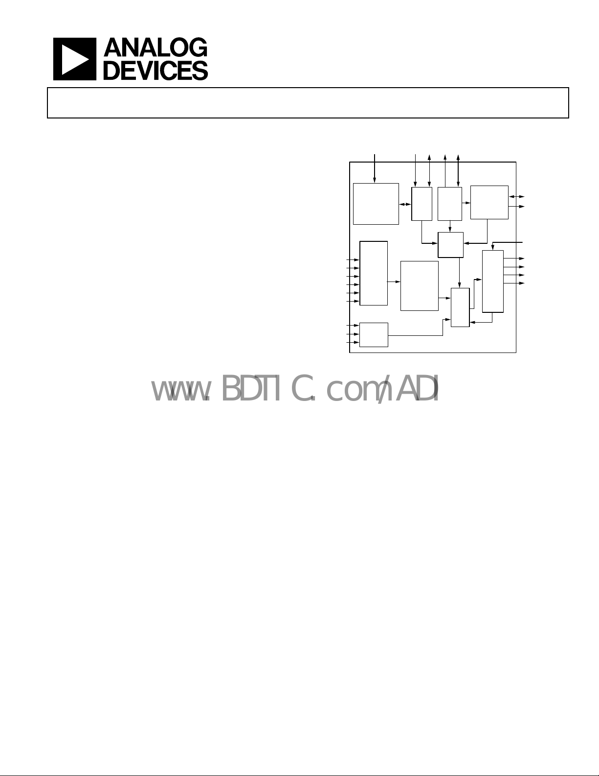
HDMI™/DVI Transmitter
AD9889
FUNCTIONAL BLOCK DIAGRAM
MDAMCL
HTPG SCL
REGISTER
CONFIGURATION
LOGIC
VIDEO
DATA
CAPTURE
AUDIO
DATA
CAPTURE
SDA
I2C
SLAVE
COLOR
SPACE
CONVERSION
4:2:2
TO
4:4:4
CONVERSION
2
C
I
MASTER
HDCP
CIPHER
MASK
Figure 1.
XOR
HDCP
CONTROLLER
HDM
ITX
CORE
AD9889
DDSDA
DDCSCL
SWING_ADJ
Tx0[1:0]
Tx1[1:0]
Tx2[1:0]
TxC[1:0]
1
0
0
-
5
7
6
5
0
APPLICATIONS
DVD players and recorders
Digital set-top boxes
AV receivers
Digital cameras and camcorders
GENERAL DESCRIPTION
The AD9889 is an 80 MHz, high-definition multimedia interface (HDMI
to 1080i and 720p, and graphic resolutions up to XGA (1024 ×
768 @ 75 Hz). With the inclusion of HDCP, the AD9889 allows
the secure transmission of protected content as specified by the
HDCP 1.1 protocol.
The AD9889 supports both S/PDIF and 8-channel I
Its high fidelity 8-channel I
7.1 surround audio at 192 kHz. The S/PDIF can carry stereo
LPCM (linear pulse code modulation) audio or compressed
audio including Dolby® Digital, DTS®, and THX®.
TM
1.1) transmitter. It supports HDTV formats up
2
2
S can transmit either stereo or
S audio.
The AD9889 helps to reduce system design complexity and cost
by incorporating such features as HDCP master, I
2
C master for
EDID reading, a single 1.8 V power supply, and 5 V tolerance
2
C and hot plug detect pins.
on I
Fabricated in an advanced CMOS process, the AD9889 is provided in a space-saving, 80-lead, surface-mount, Pb-free plastic
LQFP and is specified over the 0°C to 70°C temperature range.
EVALUATION KITS AND OTHER RESOURCES
Evaluation kits, reference design schematics, software quick
start guide, and codes are available from Analog Devices local
sales and marketing personnel.
Rev. 0
Information furnished by Analog Devices is believed to be accurate and reliable. However, no
responsibility is assumed by Anal og Devices for its use, nor for any infringements of patents or ot her
rights of third parties that may result from its use. Specifications subject to change without notice. No
license is granted by implication or otherwise under any patent or patent rights of Analog Devices.
Trademarks and registered trademarks are the property of their respective owners.
One Technology Way, P.O. Box 9106, Norwood, MA 02062-9106, U.S.A.
Tel: 781.329.4700 www.analog.com
Fax: 781.461.3113 © 2005 Analog Devices, Inc. All rights reserved.
Page 2

AD9889
www.BDTIC.com/ADI
TABLE OF CONTENTS
Features.............................................................................................. 1
2
I
S Audio...................................................................................... 17
Applications....................................................................................... 1
Functional Block Diagram .............................................................. 1
General Description ......................................................................... 1
Evaluation Kits and Other Resources ............................................ 1
Revision History ............................................................................... 2
Electrical Specifications ................................................................... 3
Absolute Maximum Ratings............................................................ 5
Explanation of Test Levels ........................................................... 5
ESD Caution.................................................................................. 5
Pin Configuration and Function Descriptions............................. 6
2
I
C Addresses ................................................................................ 8
List of Reference Documents...................................................... 8
Format Standards ......................................................................... 8
Design Guide..................................................................................... 9
General Description..................................................................... 9
S/PDIF Audio.............................................................................. 17
CTS Generation.......................................................................... 17
N Parameter................................................................................ 18
CTS Parameter............................................................................ 18
Packet Configuration................................................................. 19
Pixel Repetition .......................................................................... 19
HDCP Handling......................................................................... 20
EDID Reading............................................................................. 20
Interrupts..................................................................................... 20
Power Management ................................................................... 20
2-Wire Serial Register Map........................................................... 21
2-Wire Serial Control Register Detail Chip Identification ....... 33
Source Product Description (SPD) Infoframe....................... 37
2-Wire Serial Control Port ............................................................ 40
Data Transfer via Serial Interface............................................. 40
Video Data Capture...................................................................... 9
Input Formats................................................................................ 9
4:2:2 to 4:4:4 Data Conversion.................................................. 14
Horizontal Sync, Vertical Sync, and Degeneration................ 14
Degeneration............................................................................... 14
HSYNC and VSYNC Generation............................................. 14
Color Space Conversion Matrix (CSC) ................................... 16
Audio Data Capture ....................................................................... 17
REVISION HISTORY
10/05—Revision 0: Initial Version
Serial Interface Read/Write Examples..................................... 41
PCB Layout Recommendations.................................................... 42
Power Supply Bypassing............................................................ 42
Digital Inputs .............................................................................. 42
Color Space Converter (CSC) Common Settings...................... 43
Outline Dimensions....................................................................... 45
Ordering Guide .......................................................................... 45
Rev. 0 | Page 2 of 48
Page 3
AD9889
www.BDTIC.com/ADI
ELECTRICAL SPECIFICATIONS
Table 1.
AD9889KSTZ-80
Parameter Temp Test Level Min Typ Max Unit
DIGITAL INPUTS
Input Voltage, High (VIH) Full VI 1.4 V
Input Voltage, Low (VIL) Full VI 0.7 V
Input Current, High (VIH) Full V −1.0 mA
Input Current, Low (VIL) Full V +1.0 mA
Input Capacitance 25°C V 3 pF
DIGITAL OUTPUTS
Output Voltage, High (VOH) Full VI AVDD − 0.1 V
Output Voltage, Low (VOL) Full VI 0.4 V
THERMAL CHARACTERISTICS
θJC Junction-to-Case
Thermal Resistance V 25 °C/W
θJA Junction-to-Ambient
Thermal Resistance V 30 °C/W
Ambient Temperature Full V 0 25 70 °C
DC SPECIFICATIONS
Input Leakage Current, IIL 25°C VI −10 +10 µA
Input Clamp Voltage (−16 mA) 25°C V −0.8 V
Input Clamp Voltage (+16 mA) 25°C V +0.8
Differential High Level Output Voltage V AVCC V
Differential Output Short-Circuit Current V 10 µA
POWER SUPPLY
VDD (All) Supply Voltage Full IV 1.71 1.8 1.89 V
VDD Supply Voltage Noise Full V 50 mV p-p
Complete Power-Down Current
(Everything Except I
Quiet Power Down Current
(Monitor Detect On)
Transmitter Supply Current
(27 MHz Typical Random Pattern)
Transmitter Supply Current
(80 MHz Typical Random Pattern)
Transmitter Total Power
(80 MHz Single Pixel Stripe Pattern; Worst Case
Operating Conditions)
AC SPECIFICATIONS
CLK Frequency 25°C IV 13.5 80 MHz
CLK Duty Cycle 25°C VI 40% 60%
Worst Case CLK Input Jitter Full VI 1.0 ns
Setup Time to CLK Falling Edge VI TBD TBD ns
Hold Time to CLK Falling Edge VI TBD TBD ns
TMDS Differential Swing VII 800 1000 1200 mV
VSYNC and HSYNC Delay from DE Falling Edge VI 1 UI
VSYNC and HSYNC Delay to DE Rising Edge VI 1 UI
DE High Time 25°C VI 8191 UI
DE Low Time 25°C VI 138 UI
Differential Output Swing Low-to-High
Transition Time
Differential Swing Output High-to-Low
Transition Time
2
C)
25°C IV 6 13 mA
25°C VI 7 mA
25°C VI 165 mA
25°C IV 185 205 mA
Full VI 430 mW
25°C VII 75
25°C VII 75
490 ps
490 ps
Rev. 0 | Page 3 of 48
Page 4

AD9889
www.BDTIC.com/ADI
AD9889KSTZ-80
Parameter Temp Test Level Min Typ Max Unit
AUDIO AC TIMING
Sample Rate (I2S and S/PDIF) Full IV 32 192 kHz
I2S Cycle Time 25°C IV 1 UI
I2S Setup Time 25°C IV 15 ns
I2S Hold Time 25°C IV 0 ns
Audio Pipeline Delay 25°C IV 75 us
Rev. 0 | Page 4 of 48
Page 5
AD9889
www.BDTIC.com/ADI
ABSOLUTE MAXIMUM RATINGS
Table 2.
Parameter Rating
Digital Inputs 5 V to 0.0 V
Digital Output Current 20 mA
Operating Temperature Range −40°C to +85°C
Storage Temperature Range −65°C to +150°C
Maximum Junction Temperature 150°C
Maximum Case Temperature 150°C
Stresses above those listed under Absolute Maximum Ratings
may cause permanent damage to the device. This is a stress
rating only; functional operation of the device at these or any
other conditions above those indicated in the operational
section of this specification is not implied. Exposure to absolute
maximum rating conditions for extended periods may affect
device reliability.
EXPLANATION OF TEST LEVELS
Table 3.
Level Test
I 100% production tested.
II
III Sample tested only.
IV
V Parameter is a typical value only.
VI
VII Limits defined by HDMI specification.
100% production tested at 25°C and sample tested at
specified temperatures.
Parameter is guaranteed by design and characterization
testing.
100% production tested at 25°C; guaranteed by design
and characterization testing.
ESD CAUTION
ESD (electrostatic discharge) sensitive device. Electrostatic charges as high as 4000 V readily accumulate on
the human body and test equipment and can discharge without detection. Although this product features
proprietary ESD protection circuitry, permanent damage may occur on devices subjected to high energy
electrostatic discharges. Therefore, proper ESD precautions are recommended to avoid performance
degradation or loss of functionality.
Rev. 0 | Page 5 of 48
Page 6
AD9889
www.BDTIC.com/ADI
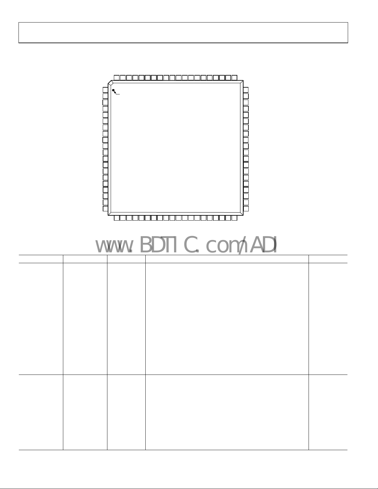
PIN CONFIGURATION AND FUNCTION DESCRIPTIONS
DD
DD
DD
GND79GND78D177D276D375D474D573D672D771D870D969D1068D1167D1266D1365D1464DV
80
DD
DV
DV
DV
63
62
61
DV
DE
HSYNC
VSYNC
CLK
S/PDIF
MCLK
I2S0
I2S1
I2S2
I2S3
SCLK
LRCLK
GND
PV
GND
GND
PV
PV
1
DD
D0
DD
DD
DD
PIN 1
2
3
4
5
6
7
8
9
10
11
12
13
14
15
16
17
18
19
20
21
22
23
24
25
26
DD
DD
EXT_SW
HPD
AV
PV
GND
AD9889
TOP VIEW
(Not to Scale)
27
28
29
30
31
32
33
GND
DD
GND
Tx0–
TxC–
TxC+
Tx0+
AV
Figure 2. Pin Configuration
34
35
36
37
38
DD
Tx1–
PD/A0
Tx1+
Tx2–
Tx2+
AV
60
GND
59
GND
58
D15
57
D16
56
D17
55
D18
54
D19
53
D20
52
D21
51
D22
50
D23
49
MCL
48
MDA
47
SDA
46
SCL
45
DDSDA
44
DDCSCL
43
GND
42
GND
41
AV
DD
39
40
INT
GND
05675-002
Table 4. Complete Pinout List
Pin Type Pin No. Mnemonic Description Value
INPUTS
50 to 58,
65 to 78, 2 D[23:0] Video Data Input 1.8 V CMOS
6 CLK Video Clock Input 1.8 V CMOS
3 DE Data Enable Bit for Digital Video 1.8 V CMOS
4 HSYNC Horizontal SYNC Input 1.8 V CMOS
5 VSYNC Vertical SYNC Input 1.8 V CMOS
23 EXT_SW Differential Output Swing Adjustment 1.8 V CMOS
25 HPD Hot Plug Detect Signal 1.8 V CMOS
7 S/PDIF S/PDIF (Sony/Philips Digital Interface) Audio Input Pin 1.8 V CMOS
8 MCLK Audio Reference Clock, 128 × fs or 256 × fs 1.8 V CMOS
12 to 9 I2S[3:0] I2S Audio Data Inputs 1.8 V CMOS
13 SCLK I2S Audio Clock 1.8 V CMOS
14 LRCLK Left/Right Channel Selection 1.8 V CMOS
33 PD/A0 Power-Down Control 1.8 V CMOS
OUTPUTS
28, 27 TxC+ Differential Clock Output TMDS
TxC− Differential Clock Output Complement
38, 37 Tx2+ Differential Output Channel 2 TMDS
Tx2− Differential Output Channel 2 Complement
35, 34 Tx1+ Differential Output Channel 1 TMDS
Tx1− Differential Output Channel 1 Complement
31, 30 Tx0+ Differential Output Channel 0 TMDS
Tx0− Differential Output Channel 0 Complement
40 INT Monitor Sense Connection Status 1.8 V CMOS
Rev. 0 | Page 6 of 48
Page 7
AD9889
www.BDTIC.com/ADI
Pin Type Pin No. Mnemonic Description Value
POWER SUPPLY
24, 29, 36, 41 AVDD Output Power Supply 1.8 V
1, 61, 62, 63, 64 DVDD Digital and I/O Power Supply 1.8 V
16, 19, 20, 21 PVDD PLL Power Supply 1.8 V
CONTROL
47 SDA Serial Port Data I/O 3.3 V CMOS
46 SCL Serial Port Data Clock (100 kHz Maximum) 3.3 V CMOS
48 MDA Serial Port Data I/O to HDCP Keys 3.3 V CMOS
49 MCL Serial Port Data Clock to HDCP Keys 3.3 V CMOS
45 DDSDA Serial Port Data I/O to Receiver 3.3 V CMOS
44 DDCSCL Serial Port Data Clock to Receiver 3.3 V CMOS
Table 5. Pin Function Descriptions
Pin Mnemonic Description
OUTPUTS
TxC+ Differential Clock Output at Pixel Clock Rate; Transition Minimized Differential Signaling (TMDS).
TxC− Differential Clock Output Complement.
Tx2+ Differential Output of the Red Data at 10× the Pixel Clock Rate; TMDS.
Tx2− Differential Red Output Complement.
Tx1+ Differential Output of the Green Data at 10× the Pixel Clock Rate; TMDS.
Tx1− Differential Green Output Complement.
Tx0+ Differential Output of the Blue Data at 10× the Pixel Clock Rate; TMDS.
Tx0− Differential Blue Output Complement.
INT Monitor Sense.
SERIAL PORT (2-WIRE)
SDA Serial Port Data I/O.
SCL Serial Port Data Clock.
DDSDA Serial Port Data I/O Master to Receiver.
DDCSCL Serial Port Data Clock Master to Receiver.
MDA Serial Port Data I/O Master to HDCP Keys.
MCL Serial Port Data Clock Master to HDCP Keys.
For a full description of the 2-wire serial register and how it works, refer to the 2-Wire Serial Control Port section.
INPUTS
D[23:0] Digital Input in RGB or YCbCr Format.
CLK Video Clock Input.
DE Data Enable for Video Data.
HSYNC Horizontal Sync Input.
VSYNC Vertical Sync Input. This is the input for vertical sync.
EXT_SW
HPD Hot Plug Detect. This indicates to the interface whether the receiver is connected.
S/PDIF S/PDIF Audio Input. This is the audio input from a Sony/Philips Digital Interface.
MCLK Audio Reference Clock. Set either to 128 × fs or 256 × fs.
I2S[3:0] I2S Audio Inputs. These represent the eight channels of audio (two per input) available through I2S.
I2S CLK I2S Audio Clock.
LRCLK Left/Right Channel Selection.
PD/A0 Power Down.
15, 17, 18, 22,
26, 32, 39, 42,
43, 59, 60, 79,
80
Swing Adjust Sets the Differential Output Voltage or Swing. An 887 Ω resistor (1% tolerance) should be placed
between this pin and ground.
GND Ground 0 V
Rev. 0 | Page 7 of 48
Page 8
AD9889
www.BDTIC.com/ADI
Pin Mnemonic Description
POWER SUPPLY
DVDD
AVDD Output Power Supply
PVDD
GND
I2C ADDRESSES
The SDA/SCL programming address is 0x72 or 0x7A based on whether A0 is pulled high (10 kΩ resistor = 0x7A) or pulled low (10 kΩ
resistor = 0x72).
The MDA/MCL EEPROM address is 0xA0.
The EDID EEPROM on the receiver is expected to have an address of 0xA0.
LIST OF REFERENCE DOCUMENTS
Table 6.
Document Description
EIA/CEA-861B Describes audio and video infoframes as well as the E-EDID structure for HDMI.
HDMI V1.1 Defining document for HDMI Version 1.1. Can be located at www.hdmi.org.
HDCPv1.0 Defining document for HDCP Version 1.1. Can be located at www.digital-cp.com.
ITU-R BT.656-3 Defining document for BT656.
Main Power Supply. These pins supply power to the main elements of the circuit. They should be filtered and as
quiet as possible.
Clock Generator Power Supply. The most sensitive portion of the AD9889 is the clock generation circuitry. These
pins provide power to the clock PLL (phase-locked loop) and help the user design for optimal performance. The
designer should provide quiet, noise-free power to these pins.
Ground. The ground return for all circuitry on-chip. It is recommended that the AD9889 be assembled on a single
solid ground plane, with careful attention given to ground current paths.
FORMAT STANDARDS
In this document, data is represented in a variety of ways.
Table 7.
Data Type Format
0xNN Hexadecimal (base-16) numbers are represented using the C language notation, preceded by 0x.
0bNN Binary (base-2) numbers are represented using the C language notation, preceded by 0b.
NN Decimal (base-10) numbers are represented using no additional prefixes or suffixes.
Bit Bits are numbered in little-endian format, that is, the least significant bit (LSB) of a byte or word is referred to as Bit 0.
Rev. 0 | Page 8 of 48
Page 9
AD9889
www.BDTIC.com/ADI
DESIGN GUIDE
GENERAL DESCRIPTION
The AD9889 HDMI transmitter provides a high bandwidth digital
content protected (HDCP) digital link between a wide range of
digital input formats—both audio and video (see Tab le 8) a nd
output
formats (see Table 9). Video and audio data are captured
and
prepared for transmission while three separate I
2
C buses (two
of which are masters) are used to program and provide content
protection for the data to be transmitted.
VIDEO DATA CAPTURE
The AD9889 can accept video data from as few as eight pins
(YCbCr DDR) representing 8-bit data or as many as 24 pins
representing 12-bit data. The AD9889 is capable of detecting
all of the 34 video formats defined in the EIA/CEA-861B
specification. If video ID (VID) 32, 33, or 34 is present, the user
needs to set Register R0x15[0] to 0b1, as these modes have V
REF
frequencies of 30 Hz or less. The user can read the detected
video format at R0x3E[7:2]. Formats outside the EIA/CEA-861B
specification can be read in R0x3F[7:5]. Detailed line count
differences for 240p and 288p modes can be read from
R0x3F[4:3]. In order to distinguish between an aspect ratio of
4:3 and one of 16:9, R0x17[1] should be set accordingly.
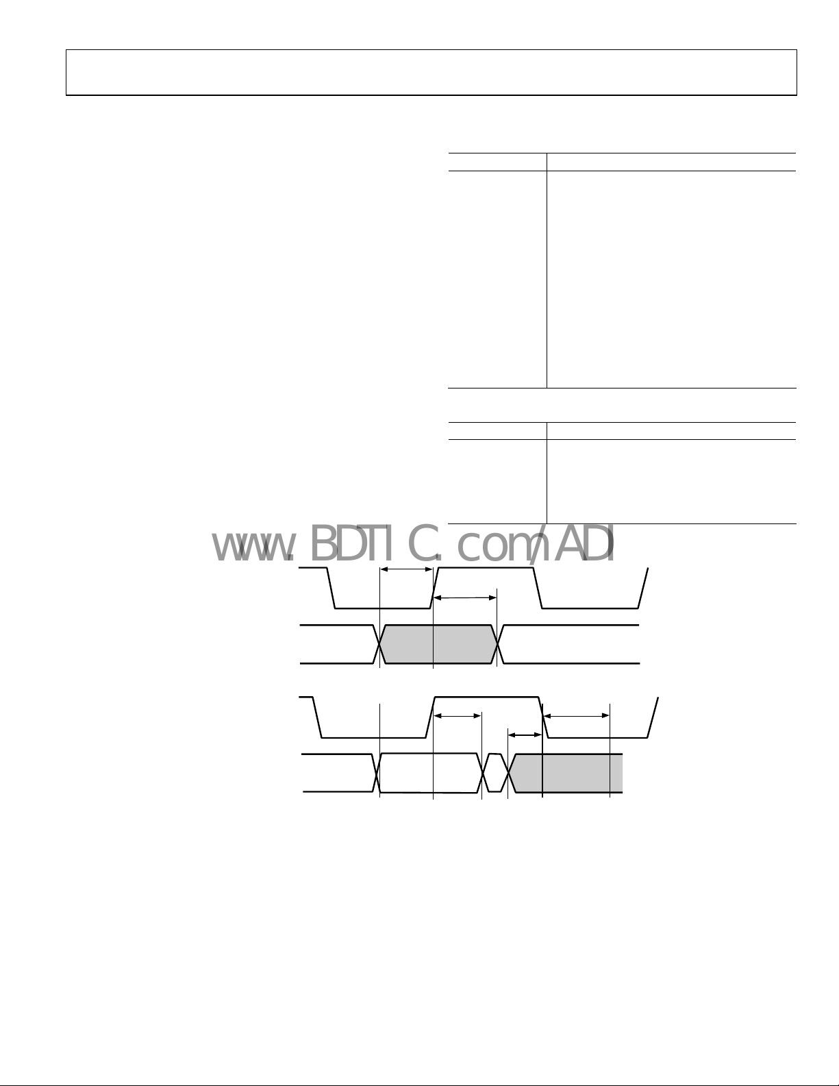
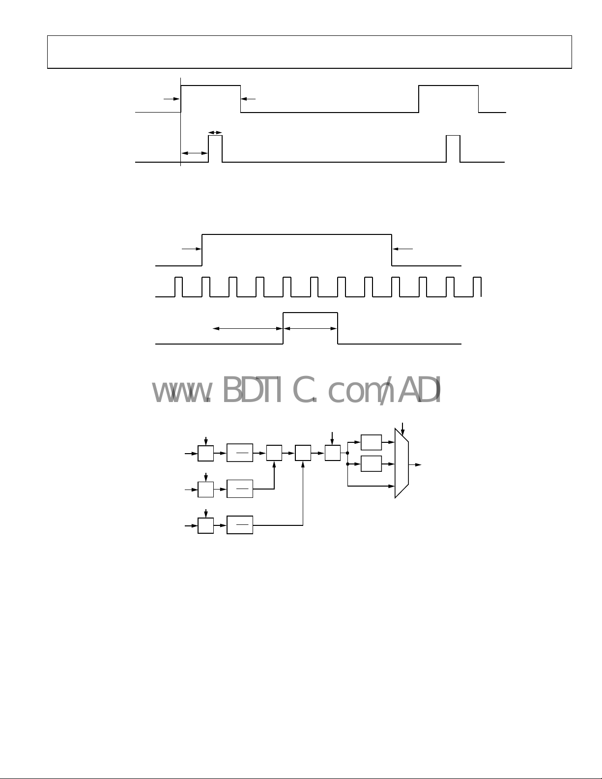
INPUT FORMATS
t
SETUP
Table 8. Input Formats Supported
No. of Bits Input Format
12 RGB (DDR)
12 YCbCr 4:4:4 (DDR)
24 RGB 4:4:4
24 YCbCr 4:4:4
16 YCbCr 4:2:2 (ITU.601)
20 YCbCr 4:2:2 (ITU.601)
24 YCbCr 4:2:2 (ITU.601)
8 YCbCr (DDR)
10 YCbCr (DDR)
12 YCbCr (DDR)
8 YCbCr 4:2:2 (ITU.656)
10 YCbCr 4:2:2 (ITU.656)
12 YCbCr 4:2:2 (ITU.656)
Table 9. Output Formats Supported
No. of Bits Output Format
24 RGB 4:4:4
24 YCbCr 4:4:4
16 YCbCr 4:2:2
20 YCbCr 4:2:2
24 YCbCr 4:2:2
INPUT CLOCK-
RISING EDGE
INPUT DATA:
D(23:0), DE, SYNCS
t
HOLD
t
HOLD
Figure 3. Timing for Data Input
t
SETUP
t
HOLD
05675-014
Rev. 0 | Page 9 of 48
Page 10
AD9889
www.BDTIC.com/ADI
Normal 4:4:4 Input Format (RGB or YCbCr) Input ID = 0
An input format of RGB 4:4:4 or YCbCr 4:4:4 can be selected by setting the input ID (R0x15[3:1]) to 0b000. The input color space (CS)
must be selected by setting R0x16[0] to 0b0 for RGB or 0b1 for YCbCr. There is no need to set the input style (R0x16[3:2]).
Table 10.
Data<23:0>
Input Format
RGB 4:4:4 R[7:0] G[7:0] B[7:0]
YCbCr 4:4:4 Cr[7:0] Y[7:0] Cb[7:0]
YCbCr 4:2:2 Formats (24 Bits, 20 Bits, or 16 Bits) with Separate Sync, Input ID = 1
An input with YCbCr 4:2:2 with separate syncs can be selected by setting the Input ID (R0x15[3:1]) to 0b001. The input CS (R0x16[0])
must be set to 0b1 for proper operation. The data bit width (24 bits, 20 bits, or 16 bits) must be set with R0x16[5:4]. The three input pin
assignment styles are shown in Table 11. The input style can be set in R0x16[3:2].
Table 11.
Data <23:0>
Input Format 23 22 21 20 19 18 17 16 15 14 13 12 11 10 9 8 7 6 5 4 3 2 1 0
YCbCr 4:2:2 Sep. Cb[11:4] Y[11:4] Cb[3:0] Y[3:0]
Sync (24 bit) Cr[11:4] Y[11:4] Cr[3:0] Y[3:0]
YCbCr 4:2:2 Sep. Cb[9:2] Y[9:2] Cb[1:0] Y[1:0]
Sync (20 bit) Cr[9:2] Y[9:2] Cr[1:0] Y[1:0]
YCbCr 4:2:2 Sep. Cb[7:0] Y[7:0]
Sync (20 bit) Cr[7:0] Y[7:0]
24-bit Cb[11:0] Y[11:0]
Cr[11:0] Y[11:0]
20-bit Cb[9:0] Y[9:0]
Cr[9:0] Y[9:0]
16-bit Cb[7:0] Y[7:0]
Cr[7:0] Y[7:0]
24-bit Y[11:0] Cb[11:0]
Y[11:0] Cr[11:0]
20-bit Y[9:0] Cb[9:0]
Y[9:0] Cr[9:0]
16-bit Y[7:0] Cb[7:0]
Y[7:0] Cr[7:0]
23 22 21 20 19 18 17 16 15 14 13 12 11 10 9 8 7 6 5 4 3 2 1 0
Style 1
Style 2
Style 3
Rev. 0 | Page 10 of 48
Page 11
AD9889
www.BDTIC.com/ADI
YCbCr 4:2:2 Formats (24 Bits, 20 Bits, or 16 Bits) with Embedded Syncs, Input ID = 2
An input with YCbCr 4:2:2 with embedded syncs can be selected by setting the input ID (R0x15[3:1]) to 0b010. HS YNC and VSYNC are
embedded as Start of Active Video (SAV) and End of Active Video (EAV). The input CS (R0x16[0]) must be set to 0b1 for proper
operation. The data bit width (24 = 12 bits, 20 = 10 bits, or 16 = 8 bits) must be set with R0x16[5:4]. The three input pin assignment styles
are shown in Table 12. The input style can be set in R0x16[3:2]. The only difference between Input ID 1 and Input ID 2 is that the syncs
n ID 2 are embedded in the data much like ITU 656 running at 1× clock and double width.
o
Table 12.
Data <23:0>
Input Format 23 22 21 20 19 18 17 16 15 14 13 12 11 10 9 8 7 6 5 4 3 2 1 0
Style 1
YCbCr 4:2:2 Sep. Cb[11:4] Y[11:4] Cb[3:0] Y[3:0]
Sync (24 bit) Cr[11:4] Y[11:4] Cr[3:0] Y[3:0]
YCbCr 4:2:2 Sep. Cb[9:2] Y[9:2] Cb[1:0] Y[1:0]
Sync (20 bit) Cr[9:2] Y[9:2] Cr[1:0] Y[1:0]
YCbCr 4:2:2 Sep. Cb[7:0] Y[7:0]
Sync (16 bit) Cr[7:0] Y[7:0]
Style 2
24-bit Cb[11:0] Y[11:0]
Cr[11:0] Y[11:0]
20-bit Cb[9:0] Y[9:0]
Cr[9:0] Y[9:0]
16-bit Cb[7:0] Y[7:0]
Cr[7:0] Y[7:0]
Style 3
24-bit Y[11:0] Cb[11:0]
Y[11:0] Cr[11:0]
20-bit Y[9:0] Cb[9:0]
Y[9:0] Cr[9:0]
16-bit Y[7:0] Cb[7:0]
Y[7:0] Cr[7:0]
YCbCr 4:2:2 Formats (Double Data Rate) Formats (12, 10, or 8 bits) with Separate Syncs, Input ID = 3
An input with YCbCr 4:2:2 DDR data and separate syncs can be selected by setting the input ID (R0x15[3:1]) to 0b011. The input CS
(R0x16 [0]) must be set to 0b1. The data bit width (12 bits, 10 bits, or 8 bits) must be set with R0x16[5:4]. The two input pin assignment
styles are shown in
Table 13.
Input Format
12-bit Cb/Y/Cr/Y[11:4] [3:0]
10-bit Cb/Y/Cr/Y[9:2] [1:0]
8-bit Cb/Y/Cr/Y[7:0]
12-bit Cb/Y/Cr/Y[11:0]
10-bit Cb/Y/Cr/Y[9:0]
8-bit Cb/Y/Cr/Y[7:0]
Table 13. The input style can be set in R0x16[3:2].
Data <23:0>
23 22 21 20 19 18 17 16 15 14 13 12 11 10 9 8 7 6 5 4 3 2 1 0
Style 1
Style 2
Rev. 0 | Page 11 of 48
Page 12
AD9889
www.BDTIC.com/ADI
YCbCr 4:2:2 DDR (Double Data Rate) Formats (12 Bits, 10 Bits, or 8 Bits) with Embedded Syncs. Input ID = 4
An input with YCbCr 4:2:2 DDR data and embedded syncs (ITU 656) can be selected by setting the input ID (R0x15[3:1]) to 0b100. The
input CS (R0x16[0]) must be set to 0b1. The data bit width (12 bits, 10 bits, or 8 bits) must be set with R0x16[5:4]. The two input pin
assignment styles are shown in Table 14. The input style can be set in R0x16[3:2]. The order of data input is the order in the table (for
exa
mple, 12-bit data is accepted as Cb0, Y0, Cr0, Y1, Cb2, Y2, Cr2, Y3).
Table 14.
Data <23:0>
Input Format
12-bit Cb/Y/Cr/Y[11:4] [3:0]
10-bit Cb/Y/Cr/Y[9:2] [1:0]
8-bit Cb/Y/Cr/Y[7:0]
12-bit Cb/Y/Cr/Y[11:0]
10-bit Cb/Y/Cr/Y[9:0]
8-bit Cb/Y/Cr/Y[7:0]
Normal 4:4:4 input format (RGB or YCbCr) Clocked at Double Data Rate (DDR), Input ID = 5
An input with YCbCr 4:2:2 DDR data and separate syncs can be selected by setting the input ID (R0x15[3:1]) to 0b011. The input CS
(R0x16[0]) must be set to 0b1. The data bit width (12 bits, 10 bits, or 8 bits) must be set with R0x16[5:4]. The three input pin assignment
styles are shown in Table 15. The input style can be set in R0x16[3:2].
Table 15.
Input Format
RGB 4:4:4 (DDR)
st
edge,
(1
nd
2
edge)
YCbCr 4:4:4 (DDR)
st
edge,
(1
nd
2
edge)
RGB 4:4:4 (DDR)
st
edge,
(1
nd
2
edge)
YCbCr 4:4:4 (DDR)
st
edge,
(1
nd
edge)
2
YCbCr 4:4:4 (DDR)
st
edge,
(1
nd
2
edge)
23 22 21 20 19 18 17 16 15 14 13 12 11 10 9 8 7 6 5 4 3 2 1 0
Style 1
Style 2
Data <23:0>
23 22 21 20 19 18 17 16 15 14 13 12 11 10 9 8 7 6 5 4 3 2 1 0
Style 1
G[3:0] B[7:0]
R[7:0] G[7:4]
Y[3:0] Cb[7:0]
Cr[7:0] Y[7:4]
Style 2
R[7:0] G[7:4]
G[3:0] B[7:0]
Cr[7:0] Y[7:4]
Y[3:0] Cb[7:0]
Style 3
Y[7:0] Cb[7:4]
Cb[3:0] Cr[7:0]
Rev. 0 | Page 12 of 48
Page 13
AD9889
www.BDTIC.com/ADI
YCbCr 4:2:2 Formats (24, 20, or 16 bits) DDR with Separate Sync, Input ID = 6
An input format of YCbCr 4:2:2 DDR can be selected by setting the input ID (R0x15[3:1]) to 0b110. The three different input pin
assignment styles are shown in Table 16. The input style can be set in R0x16[3:2]. The input CS (R0x16[0]) must be set to 0b1. The data
b
it width (12, 10, or 8 bits) must be set to with R0x16[5:4].
st
The 1
or the 2nd edge may be the rising or falling edge. The data input edge is defined in R0x16[1]. 0b0 = rising edge; 0b1 = falling edge.
Pixel 0 is the first pixel of the 4:2:2 word and should be where DE starts.
Table 16.
Data<23:0>
Input Format
YCbCr 4:2:2 Sep
Syncs (DDR)
12-bit
YCbCr 4:2:2 Sep
Syncs (DDR)
10-bit
YCbCr 4:2:2 Sep.
Syncs (DDR)
8-bit
12-bit
10-bit
8-bit
12-bit
10-bit
8-bit
23 22 21 20 19 18 17 16 15 14 13 12 11 10 9 8 7 6 5 4 3 2 1 0
Style 1
1
Y[7:4] Cr[3:0] Y[3:0]
Y[5:4] Cb[3:0] Y[3:0]
Cb[9:4] Y[9:6]
Y[5:4] Cr[3:0] Y[3:0]
Cr[9:4] Y[9:6]
Cb[3:0] Y[3:0]
Cb[7:4] Y[7:4]
Cr[3:0] Y[3:0]
Cr[7:4] Y[7:4]
Y[11:0]
Cb[11:0]
Y[11:0]
Cr[11:0]
Y[9:0]
Cb[9:0]
Y[9:0]
Cr[9:0]
Y[7:0]
Cb[7:0]
Y[7:0]
Cr[7:0]
Cb[11:0]
Y[11:0]
Cr[11:0]
Y[11:0]
Cb[9:0]
Y[9:0]
Cr[9:0]
Y[9:0]
Cb[7:0]
Y[7:0]
Cr[7:0]
Y[7:0]
1
2
st
Pixel
nd
Pixel
Cr[11:4] Y[11:8]
nd
2
Edge
st
Edge Y[7:4] Cb[3:0] Y[3:0]
Cb[11:4] Y[11:8]
Style 2
Style 3
Rev. 0 | Page 13 of 48
Page 14
AD9889
www.BDTIC.com/ADI
4:2:2 TO 4:4:4 DATA CONVERSION
The AD9889 has the ability to convert YCbCr video from 4:4:4
to 4:2:2 and 4:2:2 to 4:4:4. To convert from 4:4:4 to 4:2:2, the
video data goes through a filter first to remove any artificial
downsampling noise. To convert from 4:2:2 to 4:4:4, the
AD9889 utilizes either the zero-order upconversion (pixel
repetition) or first-order upconversion (linear interpolation).
The upconversion and downconversion are used when the
video output timing format does not match the video input
timing format. The video output format is set by Register
R0x16[7:6]. The video input format is set by the video ID
(R0x15[3:1]) and video color space (R0x16[0]). The default
mode for upconversion is pixel repetition. To use linear
interpolation, set Register R0x17[2] to 1.
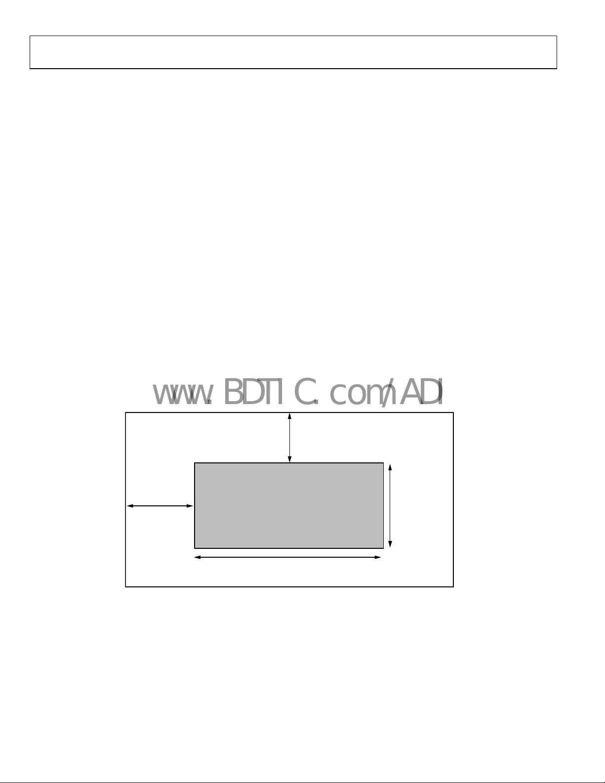
HORIZONTAL SYNC, VERTICAL SYNC, AND DEGENERATION
When transmitting video data across the TMDS interface, it
is necessary to have an HSYNC, VSYNC, and data enable (DE)
defined for the image. ITU-656 based sources have start of
active video (SAV) and end of active video (EAV) signals built
in, but the HSYNC and VSYNC must be generated (the DE is
implied by the SAV and EAV signals). Other sources (with
separate syncs) have HSYNC, VSYNC, and DE supplied at the
same time as the pixel data.
DEGENERATION
The AD9889 offers a choice of DE from an external pin, or an
internally generated DE. To activate the internal DE generation,
set Register R0x17[0] to 1. Register R0x35 to Register R0x3A
are used to define the DE. R0x35 and R0x36[7:6] define the
number of pixels from the HS leading edge to the DE leading
edge. R0x36[5:0] are the number of HSYNCs between the
leading edge of VS and DE. R0x37[7:5] defines the difference of
HS counts during VS blanking for interlace video. R0x37[4:0]
and R0x38[7:1] indicate the width of the DE. R0x39 and
R0x3A[7:4] are the number of lines of active video (see Figure
4).
HSYNC AND VSYNC GENERATION
For video with embedded HSYNC and VSYNC, such as EAV
and SAV, found in ITU 656 format, it is necessary to reconstruct
HSYNC and VSYNC. This is done with Register R0x30 to
Register R0x34. R0x30 and R0x31[7:6] specify the number of
pixels between the HSYNC leading edge and the trailing edge of
DE. Register R0x31[5:0] and Register R0x32[7:4] are the
duration of the HSYNC in pixel clocks. R0x32[3:0] and
R0x33[7:2] are the number of HS pulses between the trailing
edge of the last DE and the leading edge of the VSYNC pulse.
Register R0x33[1:0] and Register R0x34[7:0] are the duration of
VSYNC in units of HSYNCs. HSYNC and VSYNC polarity can
be specified by setting R0x17[6] (for VSYNC) and R0x17[5]
(for HSYNC).
VS DELAY
R0x36[5:0]
HS DELAY
R0x35, R0x36[7:6]
ACTIVE
VIDEO
WIDTH
R0x37[4:0], R0x38[7: 1]
Figure 4. Active Video
HEIGHT
R0x39, R0x3A[7:4]
05675-004
Rev. 0 | Page 14 of 48
Page 15
AD9889
G
www.BDTIC.com/ADI
SAV
Figure 5. HSYNC Reconstruction
05675-005
HSYNC
a: HSYNC PLACEME NT
R0x30, R0x31[7:6]
b: HSYNC DURATION
R0x31[5:0], R0x32[ 7: 4]
EAV
b
a
EAV
VSYNC
a: VSYNC PLACEMENT
R0x32[3:0], R0x33[ 7: 2]
b: VSYNC DURATI ON
R0x33[1:0], R0x34
ab
Figure 6. VSYNC Reconstruction
SAV
05675-006
a1[12:0]
1
[11:0]
R
IN
a2[12:0]
[11:0]
B
IN
a3[12:0]
[11:0]
IN
×
×
×
×
4096
1
×
4096
1
×
4096
+ + +
a4[12:0]
Figure 7. Single CSC Channel
CSC_Mode[1:0]
×4
×2
2
1
0
[11:0]
R
OUT
05675-008
Rev. 0 | Page 15 of 48
Page 16

AD9889
www.BDTIC.com/ADI
COLOR SPACE CONVERSION MATRIX (CSC)
The color space conversion matrix in the AD9889 consists of
three identical processing channels. In each channel, three
input values are multiplied by three separate coefficients. Also
included are an offset value for each row of the matrix and a
scaling multiple for all values. Each value is 13-bit, twos
complement resolution to ensure the signal integrity is
maintained. The CSC is designed to run at speeds up to
80 MHz supporting resolutions up to 1080i at 60 Hz and UXGA
at 60 Hz. With any-to-any color space support, RGB, YUV,
YCbCr, and other formats are supported by the CSC.
The main inputs, R
inputs from each channel. These inputs are based on the input
format detailed in Table 10 to Table 16. The mapping of these
in
puts to the CSC inputs is shown in Table 17.
Table 17.
Input Channel CSC Input Channel
R/Cr RIN
Gr/Y GIN
B/Cb BIN
CSC Port Mapping
, GIN, and BIN come from the 8-bit to 12-bit
IN
One of the three channels is represented in Figure 7. In each
processing channel the three inputs are multiplied by three
separate coefficients marked a1, a2, and a3. These coefficients
are divided by 4096 to obtain nominal values ranging from
−0.9998 to +0.9998. The variable labeled a4 is used as an offset
control. The CSC_Mode setting is the same for all three
processing channels. This multiplies all coefficients and offsets
by a factor of 2CSC_Mode.
The functional diagram for a single channel of the CSC as per
Figure 7 is repeated for the remaining G and B channels. The coef
ficients for these channels are b1, b2, b3, b4, c1, c2, c3, and c4.
A programming example and register settings for several
common conversions are listed in the
(CSC) C
For a detailed functional description and more programming
examples, refer to AN-795, The AD9880 Color Space Converter
User's Guide.
ommon Settings section.
Color Space Converter
Rev. 0 | Page 16 of 48
Page 17

AD9889
V
K
www.BDTIC.com/ADI
AUDIO DATA CAPTURE
The AD9889 is capable of receiving audio data in either I2S or
S/PDIF format for packetization and transmission over the
HDMI interface.
I2S AUDIO
The AD9889 can accommodate from two to eight channels of I2S
audio at up to a 192 kHz sampling rate. Selection of I
(vs. S/PDIF) is set with R0x0A[4] = 0. The detected sampling
frequency (from 32 kHz to 192 kHz) can be read in R0x04[7:4].
The output sampling frequency (from 32 kHz to 192 kHz) can be
selected with R0x15[7:4]. The number of channels and the specific
channels can be selected in R0x0C[5:2] and R0x50[7:5]. If all eight
2
channels (I
1 selects eight channels. If I
S0 to I2S3) are required, setting all bits or R0x0C[5:2] to
2
S0 only is needed, setting R0x0C[2] to 1
selects this. The placement of these packets with respect to their
output can be specified in Register R0x0E to Register R0x11.
Default settings place all channels in their respective position (I
left channel in Channel 0 left position, I
2
S3 right channel in
Channel 3 right position), but this mapping is completely
programmable.
The AD9889 supports standard I
2
justified I
S formats via R0x0C[1:0] and sample word lengths
2
S, left-justified I2S, and right-
between 16 bits and 24 bits (R0x14[3:0]).
2
S audio mode
2
S0
S/PDIF AUDIO
The AD9889 is capable of accepting two channel LPCM and
encoded audio up to a 192 kHz sampling rate via the S/PDIF.
S/PDIF audio input is selected by setting R0x0A[4] = 1. The
AD9889 is capable of accepting S/PDIF with or without an
MCLK input. When no MCLK is present, the AD9889 makes
the determination of the CTS value (N/CTS determines the
MCLK frequency).
CTS GENERATION
Audio data being carried across the HDMI link, which is driven
by a TMDS (video) clock only, does not retain the original
audio sample clock.
The task of recreating this clock at the sink is called audio clock
regeneration. There are a variety of clock regeneration methods
that can be implemented in an HDMI sink, each with a
different set of performance characteristics. The HDMI
specification does not attempt to define exactly how these
mechanisms operate. It does, however, present a possible
configuration and it does define the data items that the HDMI
source supplies to the HDMI sink in order to allow the HDMI
sink to adequately regenerate the audio clock. It also defines
how that data is generated. In many video source devices, the
audio and video clocks are generated from a common clock
(coherent clocks). In this situation, there exists a rational
(integer divided by integer) relationship between these two
clocks. The HDMI clock regeneration architecture can take
advantage of this rational relationship and can also work in an
environment where there is no such relationship between these
two clocks, that is, where the two clocks are truly asynchronous
or where their relationship is unknown.
Figure 8 shows the system architecture model used by HDMI
f
or audio clock regeneration. The source determines the
fractional relationship between the video clock and an audio
reference clock (128 × audio sample rate) and passes the
numerator and denominator for that fraction to the sink across
the HDMI link. The sink can then recreate the audio clock from
the TMDS clock by using a clock divider and a clock multiplier.
The exact relationship between the two clocks is
128 × fs = f
_clock × N/CTS
TMDS
The source determines the value of the numerator N as stated in
Section 7.2.1 of the HDMI specification. Typically, this value N
is used in a clock divider to generate an intermediate clock that
is slower than the 128 × fs clock by the factor N. The source
typically determines the value of the denominator cycle time
stamp (CTS) by counting the number of TMDS clocks in each
of the 128 × fs/N clocks.
SINK DEVICESOURCE DEVICE
DIVIDE
f
128 ×
S
IDEO CLOC
N
BY
N
REGISTER
N
1
N AND CT S VALUES ARE TRANSMITTED USI NG THE “AUDIO CLOCK REGENERATION”
PACKET. VIDEO CLOCK IS T RANSM ITTED ON T M DS CLOCK CHANNEL.
CYCLE
TIME
COUNTER
Figure 8. Audio Clock Regeneration
Rev. 0 | Page 17 of 48
CTS
TMDS
CLOCK
N
1
DIVIDE
BY
CTS
1
MULTIPLY
BY
N
128 × f
S
05675-007
Page 18

AD9889
www.BDTIC.com/ADI
N PARAMETER
N shall be an integer number that meets the following
restriction: 128 × fs/1500 Hz ≤ N ≤ 128 × fs/300 Hz with a
recommended optimal value of 128 × fs/1000 Hz equals N.
For coherent audio and video clock sources, use Table 18 to
Table 20 to determine the value of N. For noncoherent sources
r sources where coherency is not known, use the equations
o
previously described.
CTS PARAMETER
CTS is an integer number that satisfies the following:
(Average CT S Value) = (f
Recommended N and Expected CTS Values
The recommended value of N for several standard pixel clocks
is given in Table 18 to Table 20. It is recommended that sources
th noncoherent clocks use the values listed for the pixel clock
wi
type labeled Other.
Table 19. Recommended N and Expected CTS Values for 44.1 kHz Audio and Multiples
44.1 kHz 88.2 kHz 176.4 kHz
Pixel Clock (MHz) N CTS N CTS N CTS
25.1/1.001 7007 31250 14014 31250 28028 31250
25.2 6272 28000 12544 28000 25088 28000
27 6272 3000 12544 30000 25088 30000
27 × 1.001 6272 30030 12544 30030 25088 30030
54 6272 60000 12544 60000 25088 60000
54 × 1.001 6272 60060 12544 60060 25088 60060
74.25/1.001 17836 234375 35672 234375 71344 234375
74.25 6272 82500 12544 82500 25088 82500
148.5/1.001 8918 234975 17836 234375 35672 123375
148.5 6272 165000 12544 16500 25088 162000
Other 6272 Measured 15244 Measured 25088 Measured
Table 20. Recommended N and Expected CTS Values for 48 kHz Audio and Multiples
44.1 kHz 88.2 kHz 176.4 kHz
Pixel Clock (MHz) N CTS N CTS N CTS
25.1/1.001 6864 28125 13728 28125 27456 28125
25.2 6144 25200 12288 25200 24576 25200
27 6144 27000 12288 27027 24576 27027
27 × 1.001 6144 27027 12288 27027 24576 27027
54 6144 54000 12288 54000 24576 54000
54 × 1.001 6144 54054 12288 54054 24576 74250
74.25/1.001 11648 140625 23296 140625 46592 140625
74.25 6144 74250 12288 74250 24576 74250
148.5/1.001 5824 140625 11648 140625 23296 140625
148.5 6144 148500 12288 148500 24576 148500
Other 6144 Measured 12288 Measured 24576 Measured
_clock × N)/(128 × fs)
TMDS
Table 18. Recommended N and Expected CTS Values for
32 kHz Audio
32 kHz
Pixel Clock (MHz) N CTS
25.1/1.001 4576 28125
25.2 4096 25200
27 4096 27000
27 × 1.001 4096 27027
54 4096 54000
54 × 1.001 4096 54054
74.25/1.001 11648
74.25 4096 74250
148.5/1.001 11648 421875
148.5 4096 148500
Other 4096 Measured
1
This value alternates because of the restriction on N.
210937 to
1
210938
Rev. 0 | Page 18 of 48
Page 19

AD9889
www.BDTIC.com/ADI
The AD9889 has two modes for CTS generation: manual mode
and auto mode. In manual mode, the user can program the CTS
number directly into the chip (R0x07 to R0x09) and select this
external mode by setting R0x0A[7] to 1. In auto mode, the chip
computes the CTS based on the actual audio and video rates.
This can be selected by setting R0x0A[7] to 0, and the results
can be read from R0x04 to R0x06. Manual mode is good for
coherent audio and video, where the audio and video clock are
generated from the same crystal; thus CTS should be a fixed
number. The auto mode is good for incoherent audio-video,
where there is no simple integer ratio between the audio and
video clock. A filter is available (R0x0A[6:5]) to stabilize the
chip-generated CTS. The 20-bit N value can be programmed
into the AD9889 in Register R0x01 to Register R0x03.
PACKET CONFIGURATION
The AD9889 supports all the packets listed in the HDMI 1.1
specification. Each packet can be separately enabled and disabled. Based on the audio and video input, the packets are
added to the HDMI link at the earliest time, so that a minimum
delay is incurred. Notice the ISRC1 packet has one bit to enable
the ISRC2 packet. For the general control packet, remember to
clear or reset the bits to avoid system lock-up.
Table 21. Pixel Repetition—Valid Pixel Repeat Values for Each Format
Video Code Video Description EIA/CEA-861B Pixel Repeat Values HDMI Pixel Repeat Values
1 640 × 480p @ 60 Hz No repetition No repetition
2, 3 720 × 480p @ 59.94/60 Hz No repetition No repetition
4 1280 × 720p @ 59.94/60 Hz No repetition No repetition
5 1920 × 1080i @ 59.94/60 Hz No repetition No repetition
6, 7 720/1440 × 480i @ 59.94/60 Hz Pixel sent 2 times Pixel sent 2 times
8, 9 720/1440 × 240p @ 59.94/60 Hz Pixel sent 2 times Pixel sent 2 times
10, 11 2880 × 480i @ 59.94/60 Hz Pixel sent 0 to 10 times Pixel sent 1 to 10 times
12, 13 2880 × 240p @ 59.94/60 Hz Pixel sent 1 to 10 times Pixel sent 1 to 10 times
14, 15 1440 × 480p @ 59.94/60 Hz No repetition Pixel sent 1 to 2 times1
16 1920 × 1080p @ 59.94/60 Hz No repetition No repetition
17, 18 720 × 576p @ 50 Hz No repetition No repetition
19 1280 × 720p @ 50 Hz No repetition No repetition
20 1920 × 1080i @ 50 Hz No repetition No repetition
21, 22 720/1440 × 576i @ 50 Hz Pixel sent 2 times Pixel sent 2 times
23, 24 720/1440 × 288p @ 50 Hz Pixel sent 2 times Pixel sent 2 times
25, 26 2880 × 576i @ 50 Hz Pixel sent 1 to 10 times Pixel sent 1 to 10 times
27, 28 2880 × 288 @ 50 Hz Pixel sent 1 to 10 times Pixel sent 1 to 10 times
29, 30 1440 × 576p @ 50 Hz No repetition Pixel sent 1 to 2 times1
31 1920 × 1080p @ 50 Hz No repetition No repetition
32 1920 × 1080p @ 23.97/24 Hz No repetition No repetition
33 1920 × 1080p @ 25 Hz No repetition No repetition
34 1920 × 1080p @ 29.9/30 Hz No repetition No repetition
1
Denotes change from EIA/CEA-861B valid values. Pixel repetition is required to support some audio formats at 720 × 480p and 720 × 576p video format timings.
PIXEL REPETITION
Due to HDMI specification and bandwidth requirements,
sometimes it is necessary to set clock multiplication by 2× and
4× in order to maintain the minimum TMDS clock frequency.
The AD9889 offers three choices for the user to implement this
function: auto mode, manual mode, and max mode
(R0x3B[6:5]).
For the auto mode (R0x3B[6:5] = 00), based on the input video
format (either programmed by user, or chip detection) and
audio sampling rate, AD9889 automatically sets the pixel
repetition factor (R0x3D[7:6]).
For manual mode (R0x3B[6:5] = 1×), the user programs the
pixel repetition factor in R0x3B[4:3].
For max mode (R0x3B[6:5] = 01), based on the input video
format, the AD9889 selects the maximum repetition factor. The
advantage of the max mode is that it is independent of the audio
sampling rate.
Rev. 0 | Page 19 of 48
Page 20

AD9889
www.BDTIC.com/ADI
HDCP HANDLING
The AD9889 has a built-in microcontroller to handle HDCP
transmitter states, including handling downstream HDCP
repeaters. To activate HDCP from a system level, the main
controller needs to set R0xAF[7] to 1 to inform AD9889 that
the video stream should be encrypted. The AD9889 takes
control from there and implements all remaining tasks defined
by the HDCP 1.1 specification.
The system controller should monitor the status of HDCP by
reading Register R0xB8[6] (indicating the HDCP link has been
established). There are also some error flags (R0xC5[7] and
R0xC8[7:4]) to help debug the system.
The AD9889 also supports AV functions to suspend HDCP
temporarily. To set AV mute, clear R0x45[7] and set R0x45[6]
to 1. To clear AV mute, clear R0x45[6] and set R0x45[7] to 1.
(Note that it is invalid to set the two mute bits at the same time.)
For more information, refer to application note AN-810, EDID
and HDCP Controller User Guide for the AD9889.
EDID READING
The AD9889 has an I2C master (DDC Pin 44 and Pin 45) to
read the EDID based on system need. It buffers segment 0 once
HPD is detected. The system can request other segments by
programming Register R0xC4. An interrupt bit (R0x96[2])
indicates the completion of EDID rebuffering.
To read EDID data from the AD9889, use the AD9889
programming bus (Pin 46 and Pin 47) with I
This is the default address but can be changed by writing the
desired address into Register R0x43.
For more information, refer to application note AN-810, EDID
and HDCP Controller User Guide for the AD9889.
2
C Address 0x7E.
INTERRUPTS
The AD9889 has interrupts to help with the system design: hot
plug detection, receiver sense, VS detection, audio FIFO
overflow, ITU 656 error, EDID ready, HDCP error, and BKSV
ready. Interrupts can be cleared by writing 1 into the interrupt
register (R0x96, R0x97). There are read-only registers (R0xC5,
R0xC6) to show the state of these signals. Masks (R0x94,
R0x95) are available to let the user selectively activate each
interrupt. To enable a specific interrupt register, write 1 to the
corresponding mask bit.
POWER MANAGEMENT
The AD9889 power-down pin polarity depends on the
AD9889’s I
active. To use 0x7A, the PD pin is low active. At any time, the
power-down pin polarity can be verified by reading Register
R0x42[7].
The AD9889 can be powered down or reset either by Pin 33 or
by Register R0x41[6]. During power-down mode, all the
circuits are inactive except the I
related to mode and activity detection. During power-down
mode, the chip status can still be read through the I
enter normal power-down mode, either drive Pin 33 to 1, or set
R0x41[6] to 1. To further reduce power consumption, disable
the receiver sense detection by setting Register R0xA4[2] to 1.
For HDCP security reasons, the I
reset by the power-down pin. Anytime after power down, the
user needs to drive the PD pin back to 0 and set R0x41[6] to
0 to activate the chip.
2
C address selection. To use 0x72, the PD pin is high
2
C slave and some circuits
2
C slave. To
2
C power-down bit is also
Rev. 0 | Page 20 of 48
Page 21

AD9889
www.BDTIC.com/ADI
2-WIRE SERIAL REGISTER MAP
The AD9889 is initialized and controlled by a set of registers that determine the operating modes. An external controller is employed to
write and read the control registers through the two-line serial interface port.
Table 22. Control Register Map
Hex
Address
0x00 Read [7:0] 00000000 Chip Revision Revision of the chip, start from 0.
0x01 Read/Write [3:0] ****0000 N[19:16]
0x02 Read/Write [7:0] 00000000 N[15:8] The middle byte of N.
0x03 Read/Write [7:0] 00000000 N[7:0] The lower byte of N.
0x04 Read
0x05 Read [7:0] 00000000 CTS_Int[15:8] Middle byte of measured CTS.
0x06 Read [7:0] 00000000 CTS_Int[7:0] Low byte of measured CTS.
0x07 Read/Write [3:0] ****0000 CTS_Ext[19:16]
0x08 Read/Write [7:0] 00000000 CTS_Ext[15:8] Middle byte of external CTS.
0x09 Read/Write [7:0] 00000000 CTS_Ext[7:0] Low byte of external CTS.
0x0A Read/Write
Read/Write or Read
Only
Default
Bits
Value
[7:4] 0000**** S/PDIF_SF
[3:0] ****0000 CTS_Int[19:16]
[7] 0******* CTS_Sel CTS source select.
[6:5] *10***** Avg_Mode CTS filter mode.
[4] ***0**** Audio_Sel Audio type select.
[3] ****0*** MCLK_SP MCLK for S/PDIF.
[2] *****0** MCLK_I2S MCLK for I2S.
[1:0] ******01 MCLK_Ratio MCLK ratio.
Register Name
Rev. 0 | Page 21 of 48
Description
20-bit N used with cycle time stamp (CTS) (see Ta ble 18
to Table 20 for appropriate settings) to regenerate the
udio clock in the receiver. For remaining bits, see
a
R0x02 and R0x03. Used only with I2S audio, not S/PDIF.
S/PDIF sampling frequency for S/PDIF audio decoded
from hardware. This information is used by both the
audio Rx and the pixel repetition.
0011 = 32 kHz.
0000 = 44.1 kHz.
0010 = 48 kHz.
1000 = 88.2 kHz.
1010 = 96 kHz.
1100 = 176.4 kHz.
1110 = 192 kHz.
Default = 0x0.
CTS measured (internal). This 20-bit value is used in
the receiver with the N value to regenerate an audio
clock. For remaining bits, see R0x05 and R0x06.
CTS (external). This 20-bit value is used in the receiver
with the N value to regenerate an audio clock. For
remaining bits see R0x08 and R0x09.
0 = internal CTS.
1 = external CTS.
Default = 0.
00 = no filter.
01 = divide by 4.
10 = divide by 8.
11 = divide by16.
Default = 10.
2
S.
0 = I
1 = S/PDIF.
Default = 0.
1 = MCLK active.
0 = MCLK inactive.
Default = 0.
2
S MCLK active.
1 = I
2
S MCLK inactive.
0 = I
Default = 0.
Page 22

AD9889
www.BDTIC.com/ADI
Hex
Address
0x0B Read/Write
Read/Write or Read
Only
Default
Bits
Value
[6] *0****** MCLK_Pol MCLK polarity.
[5] **0***** Flat_Line Flat line.
Register Name
Description
00 = × 128 fs.
01 = × 256 fs.
10 = × 384 fs.
11 = × 512 fs.
Default = 01.
0 = rising edge.
1 = falling edge.
Default = 0.
1 = flat line audio (audio sample not valid).
0 = normal.
Default = 0.
[4:0] ****0111
0x0C Read/Write
0x0D Read/Write [4:0] ***11000 I2S_bit_width
0x0E Read/Write
[5:2] **1111** I2S enable I2S enable for the four I2S pins (active).
[1:0] ******00 I
[5:3] **000*** SUBPKT0_L_src
Tes t b its
2
S Format I2S format.
Must be set to 0x7 for proper operation.
0001 = I2S0.
0010 = I
0100 = I
1000 = I
Default = 1111 for all.
00 = standard I2S mode.
01 = right-justified I
10 = left-justified I
11 = raw IEC60958 mode.
Default = 0.
2
S bit width. For right justified audio only. Default is
I
24. Not valid for widths greater than 24.
Registers 0x0E-0x11 should be set based on the
2
2
2
S1.
S2.
S3.
2
S mode.
2
S mode.
speaker mapping information obtained from EDID
Source of sub packet 0, left channel. Default = 000.
[2:0] *****001 SUBPKT0_R_src Source of sub packet 0, right channel. Default = 001.
[5:3] **010*** SUBPKT1_L_src Source of sub packet 1, left channel. Default = 010. 0x0F Read/Write
[2:0] *****011 SUBPKT1_R_src Source of sub packet 1, right channel. Default = 011.
[5:3] **100*** SUBPKT2_L_src Source of sub packet 2, left channel. Default = 100. 0x10 Read/Write
[2:0] *****101 SUBPKT2_R_src Source of sub packet 2, right channel. Default = 101.
[5:3] **110*** SUBPKT3_L_src Source of sub packet 3, left channel. Default = 110. 0x11 Read/Write
[2:0] *****111 SUBPKT3_R_src Source of sub packet 3, right channel. Default = 111.
0x12 Read/Write
0x13 Read/Write [7:0] 00000000 Category Code Category code for audio infoframe; see IEC 60958.
[5] **0***** CR_bit Copyright bit.
0 = copyright.
1 = not copyright protected.
[4:2] ***000** a_info
[1:0] ******00 Clk_Acc Clock accuracy.
Rev. 0 | Page 22 of 48
Additional information for channel status bits.
000 = 2 audio channels without pre-emphasis.
100 = 2 audio channels with 50/15 s pre-emphasis.
010 = reserved.
110 = reserved.
Default = 000.
00 = Level II, normal accuracy ±1000 × 10
01 = Level III, variable pitch shifted clock.
10 = Level I, high accuracy ±50 × 10
11 = reserved.
Default = 00.
-6.
-6.
Page 23

AD9889
www.BDTIC.com/ADI
Hex
Address
0x15 Read/Write
0x16 Read/Write [7:6] 00****** VFE_out_fmt
[5:4] **00**** VFE_422_width 4:2:2 input, could be either 8 bit, 10 bit, or 12 bit.
[3:2] ****00** VFE_input_style
Read/Write or Read
Only
Default
Bits
Value
[7:4] 0000**** Source Number Source number. 0x14 Read/Write
[3:0] ****0000 Word Length Audio word length.
[7:4] 0000**** I2S_SF
[3:1] ****000* VFE_input_id Input video format.
[0] *******0 low_frq_video Video refresh rate.
Register Name
Rev. 0 | Page 23 of 48
Description
0000 = not specified.
0100 = 16 bits.
0011 = 17 bits.
0010 = 18 bits.
0001 = 19 bits.
0101 = 20 bits.
1000 = not specified.
1100 = 20 bits.
1011 = 21 bits.
1010 = 22 bits.
1001 = 23 bits.
1101 = 24 bits.
Default = 0x0.
Sampling frequency for I
used by both the audio Rx and the pixel repetition.
0011 = 32 kHz.
0000 = 44.1 kHz.
0010 = 48 kHz.
1000 = 88.2 kHz.
1010 = 96 kHz.
1100 = 176.4 kHz.
1110 = 192 kHz.
Default = 0x0.
000 = RGB and YCbCr 4:4:4 (Y on Green).
001 = YCbCr 4:2:2; 16, 20, and 24 bit.
010 = Same as 001 with HS and VS embedded as SAV
and EAV.
011 = ITU656 with separated syncs.
100 = ITU656 with embedded syncs.
101 = DDR RGB 4:4:4 or YCbCr 4:4:4.
110 = DDR YCbCr 4:2:2.
111 = undefined.
Default = 000.
0 = V
> 30 Hz.
REF
≤ 30 Hz refresh rate video.
1 = V
REF
Default = 0.
Video output format. This should be written along
with R0x45[5:4].
00 = RGB 4:4:4.
01 = YCbCr 4:4:4.
1x = YCbCr 4:2:2.
Default = 00.
x0 = 12 bits.
01 = 10 bits.
11 = 8 bits.
Default = 00.
Styles refer to the input pin assignments. See Table 23
to Table 28.
yle 1.
x0 = St
01 = Style 2.
11 = Style 3.
2
S audio. This information is
Page 24

AD9889
www.BDTIC.com/ADI
Hex
Address
[1] ******0* VFE_input_edge
[0] *******0 VFE_input_cs Video input color space.
0x17 Read/Write
0x18 Read/Write [4:0] ***00110 CSC_A1_MSB MSB of R0x19.
0x19 Read/Write [7:0] 01100010 CSC_A1_LSB
0x1A Read/Write [4:0] ***00100 CSC_A2_MSB MSB of R0x1B.
0x1B Read/Write [7:0] 10101000 CSC_A2_LSB
0x1C Read/Write [4:0] ***00000 CSC_A3_MSB MSB of R0x1D.
0x1D Read/Write [7:0] 00000000 CSC_A3_LSB
0x1E Read/Write [4:0] ***11100 CSC_A4_MSB MSB of R0x1F.
Read/Write or Read
Only
Default
Bits
Value
[7] 0******* itu_error_correct_en
[6] *0****** itu_vsync_pol
[5] **0***** itu_hsync_pol
[4:3] ***00*** csc_mode
[2] *****0** gen_444_en 4:2:2 to 4:4:4 upconversion mode.
[1] ******0* ASP_ratio
[0] *******0 deGen_en
Register Name
Description
Video data input edge. Defines the first clock edge of
video word clocked.
0 = rising edge.
1 = falling edge.
Default = 0 (in reference to DDR).
0 = RGB.
1 = YCbCr.
Default = 0.
ITU656 error correction. This must be enabled if using
ITU656 format.
0 = disable.
1 = enable.
Default = 0.
VS polarity from regenerated ITU 656 input.
0 = high polarity.
1 = low polarity.
Default = 0.
HS polarity from regenerated ITU 656 input.
0 = high polarity.
1 = low polarity.
Default = 0.
Sets the fixed point position of the CSC coefficients,
including the a4, b4, and c4 offsets.
00 = ±1.0, −4096<−>4095.
01 = ±2.0, −8192<−>8190.
1× = ±4.0, −16384<−>16380.
Default = 000.
1 = uses interpolation.
0 = no interpolation.
Default = 0.
Aspect ratio of input video.
0 = 4:3.
1 = 16:9.
Default = 0.
Enable DE generator. The DE generator should be
enabled when a DE input is not provided.
1 = enable DE generator.
Default = 0 (see Register 0x30 to Register 0x3A).
Color space converter (CSC) coefficient for equation:
= (a1 × RIN) + (a2 × GIN) + (a3 × BIN) + a4
R
OUT
= (b1 × RIN) + (b2 × GIN) + (b3 × BIN) + b4
G
OUT
B
= (c1 × RIN) + (c2 × GIN) + (c3 × BIN) + c4
OUT
CSC coefficient for equation:
= (a1 × RIN) + (a2 × GIN) + (a3 × BIN) + a4
R
OUT
= (b1 × RIN) + (b2 × GIN) + (b3 × BIN) + b4
G
OUT
B
= (c1 × RIN) + (c2 × GIN) + (c3 × BIN) + c4
OUT
CSC coefficient for equation:
= (a1 × RIN) + (a2 × GIN) + (a3 × BIN) + a4
R
OUT
= (b1 × RIN) + (b2 × GIN) + (b3 × BIN) + b4
G
OUT
B
= (c1 × RIN) + (c2 × GIN) + (c3 × BIN) + c4
OUT
Rev. 0 | Page 24 of 48
Page 25

AD9889
www.BDTIC.com/ADI
Hex
Address
0x1F Read/Write [7:0] 10000100 CSC_A4_LSB
0x20 Read/Write [4:0] ***11100 CSC_B1_MSB MSB of R0x21.
0x21 Read/Write [7:0] 10111111 CSC_B1_LSB
0x22 Read/Write [4:0] ***00100 CSC_B2_MSB MSB of R0x23.
0x23 Read/Write [7:0] 10101000 CSC_B2_LSB
0x24 Read/Write [4:0] ***11110 CSC_B3_MSB MSB of R0x25.
0x25 Read/Write [7:0] 01110000 CSC_B3_LSB
0x26 Read/Write [4:0] ***00010 CSC_B4_MSB MSB of R0x27.
0x27 Read/Write [7:0] 00011110 CSC_B4_LSB
0x28 Read/Write [4:0] ***00000 CDC_C1_MSB MSB of R0x29.
0x29 Read/Write [7:0] 00000000 CSC_C1_LSB
0x2A Read/Write [4:0] ***00100 CSC_C2_MSB MSB of R0x2B.
0x2B Read/Write [7:0] 10101000 CSC_C2_LSB
0x2C Read/Write [4:0] ***01000 CSC_C3_MSB MSB of R0x2D.
0x2D Read/Write [7:0] 00010010 CSC_C3_LSB
0x2E Read/Write [4:0] ***11011 CSC_C4_MSB MSB of R0x2F.
0x2F Read/Write [7:0] 10101100 CSC_C4_LSB
0x30 Read/Write [7:0] 00000000 VFE_hs_pla_MSB
0x34 Read/Write [7:0] 00000000 VFE_vs_dur_LSB VSYNC duration lower 8 bits (see R0x33).
0x35 Read/Write [7:0] 00000000 VFE_hsDelayIn_MSB
Read/Write or Read
Only
Bits
Default
Value
Register Name
Description
CSC coefficient for equation:
= (a1 × RIN) + (a2 × GIN) + (a3 × BIN) + a4
R
OUT
= (b1 × RIN) + (b2 × GIN) + (b3 × BIN) + b4
G
OUT
B
= (c1 × RIN) + (c2 × GIN) + (c3 × BIN) + c4
OUT
CSC coefficient for equation:
= (a1 × RIN) + (a2 × GIN) + (a3 × BIN) + a4
R
OUT
G
= (b1 × RIN) + (b2 × GIN) + (b3 × BIN) + b4
OUT
= (c1 × RIN) + (c2 × GIN) + (c3 × BIN + c4
B
OUT
CSC coefficient for equation:
= (a1 × RIN) + (a2 × GIN) + (a3 × BIN) + a4
R
OUT
= (b1 × RIN) + (b2 × GIN) + (b3 × BIN) + b4
G
OUT
B
= (c1 × RIN) + (c2 × GIN) + (c3 × BIN) + c4
OUT
CSC coefficient for equation:
= (a1 × RIN) + (a2 × GIN) + (a3 × BIN) + a4
R
OUT
= (b1 × RIN) + (b2 × GIN) + (b3 × BIN) + b4
G
OUT
B
= (c1 × RIN) + (c2 × GIN) + (c3 × BIN) + c4
OUT
CSC coefficient for equation:
R
= (a1 × RIN) + (a2 × GIN) + (a3 × BIN) + a4
OUT
= (b1 × RIN) + (b2 × GIN) + (b3 × BIN) + b4
G
OUT
B
= (c1 × RIN) + (c2 × GIN) + (c3 × BIN) + c4
OUT
CSC coefficient for equation:
R
= (a1 × RIN) + (a2 × GIN) + (a3 × BIN) + a4
OUT
= (b1 × RIN) + (b2 × GIN) + (b3 × BIN) + b4
G
OUT
= (c1 × RIN) + (c2 × GIN) + (c3 × BIN) + c4
B
OUT
CSC coefficient for equation:
R
= (a1 × RIN) + (a2 × GIN) + (a3 × BIN) + a4
OUT
= (b1 × RIN) + (b2 × GIN) + (b3 × BIN) + b4
G
OUT
= (c1 × RIN) + (c2 × GIN) + (c3 × BIN) + c4
B
OUT
CSC coefficient for equation:
R
= (a1 × RIN) + (a2 × GIN) + (a3 × BIN) + a4
OUT
= (b1 × RIN) + (b2 × GIN) + (b3 × BIN) + b4
G
OUT
= (c1 × RIN) + (c2 × GIN) + (c3 × BIN) + c4
B
OUT
CSC coefficient for equation:
R
= (a1 × RIN) + (a2 × GIN) + (a3 × BIN) + a4
OUT
= (b1 × RIN) + (b2 × GIN) + (b3 × BIN) + b4
G
OUT
= (c1 × RIN) + (c2 × GIN) + (c3 × BIN) + c4
B
OUT
Most significant 8 bits for HSYNC placement for ITU
656 HSYNC regeneration.
[7:6] 00****** VFE_hs_pla_LSB HSYNC placement lower 2 bits (see R0x30). 0x31 Read/Write
[5:0] **000000 VFE_hs_dur_MSB Most significant 6 bits for HSYNC duration.
[7:4] 0000**** VFE_hs_dur_LSB HSYNC duration lower 4 bits (see R0x31). 0x32 Read/Write
[3:0] ****0000 VFE_vs_pla_MSB
Most significant 4 bits for VSYNC placement for ITU
656 VSYNC regeneration.
[7:2] 000000** VFE_vs_pla_LSB VSYNC placement lower 6 bits (see R0x32). 0x33 Read/Write
[1:0] ******00 VFE_vs_dur_MSB Most significant 2 bits for VSYNC duration.
Most significant 8 bits for HSYNC delay in for ITU 656
HSYNC regeneration.
Rev. 0 | Page 25 of 48
Page 26

AD9889
www.BDTIC.com/ADI
Hex
Address
0x37 Read/Write
0x38 Read/Write [7:1] 0000000* VFE_width Lower 7 bits for frame width (see R0x37).
0x39 Read/Write [7:0] 00000000 VFE_height_MSB Most significant 8 bits for frame height.
0x3A Read/Write [7:4] 0000**** VFE_height Lower 4 bits for frame height (see R0x39).
0x3B Read/Write
0x3C Read/Write [5:0] **000000 ext_VID_to_Rx
0x3E Read [7:2] 000000** VFE_fmt_VID VID detected by video FE (see Table 24).
0x3F Read
Read/Write or Read
Only
Default
Bits
Value
[7:6] 00****** VFE_hsDelayIn_LSB HSYNC delay in lower 2 bits (see R0x35). 0x36 Read/Write
[5:0] **000000 VFE_vsDelayIn VSYNC delay in for DE generation.
[7:5] 000***** Interlace Offset
[4:0] ***00000 VFE_width_MSB Most significant 5 bits for frame width.
[7] 1******* ext_audioSF_sel Audio sampling frequency select.
[6:5] *00***** pr_mode
[4:3] ***00*** ext_PLL_pr
[2:1] *****00* ext_target_pr
[0] *******0 csc_en CSC enable.
[7:6] 00****** pr_to_Rx The actual pixel repetition sent to Rx. 0x3D Read
[5:0] **000000 VID_to_Rx The actual VID sent to HDMI Rx (see Table 24).
[7:5] 000***** VFE_aux_vid
[4:3] ***00*** VFE_prog_mode Information about 240p and 288p.
Register Name
Rev. 0 | Page 26 of 48
Description
Sets the difference (in HSYNCs) in field length
between Field 0 and Field 1.
valid when using SPDIF input
0 = Fs extracted from SPDIF
1 = Fs set via R0x15[7:4]
Default = 1 (only used during pixel repetition mode).
Pixel repetition mode selection. Set to b00 unless
non-standard video is supported.
00 = auto mode.
01 = max mode.
1x = manual mode (see R0x3B Bits [4:3]).
Default = 00.
External value for PLL pixel repetition.
00 = ×1.
01 = ×2.
10 = ×4.
11 = ×4.
Default = 00.
User programmed pixel repetition number to send to
RX. Default = 00.
0 = no CSC.
1 = enable CSC.
Default = 0.
User programmed VID to send to Rx. See Table 24 for
VID formats. Default = 0x00.
full
This register is for video input formats that are not
inside the 861B table.
000 = 480i not active.
001 = 240p not active.
010 = 576i not active.
011 = 288p not active.
100 = 480i active.
101 = 240p active.
110 = 576i active.
111 = 288p active.
Default = 000.
240p – 01 = 262 lines.
240p – 10 = 263 lines.
288p – 01 = 312 lines.
288p – 10 = 313 lines.
288p – 11 = 314 lines.
Default = 00.
Page 27

AD9889
www.BDTIC.com/ADI
Hex
Address
0x40 Read/Write
0x41 Read/Write [6] *1****** system_PD
[5] **0***** Test bit Must be set to 0.
[3] ****0*** initiate_scan 1 = initiate scan. Default = 1.
0x42 Read
0x43 Read/Write [7:0] 01111110 EDID_ID The I2C address for EDID memory. Default = R0x7E.
0x44 Read/Write
0x45 Read/Write
0x46 Read/Write [7:6] 00****** Scan Information S[1:0].
Read/Write or Read
Only
[4] ***1**** INTR_pol Interrupt polarity.
Default
Bits
Value
[7] 0******* GC_pkt_en 1 = enable General Control packet. Default = 0.
[6] *0****** SPD_pkt_en
[5] **0***** MPEG_pkt_en 1 = enable MPEG packet. Default = 0.
[4] ***0**** ACP_pkt_en 1 = enable ACP packet. Default = 0.
[3] ****0*** ISRC_pkt_en 1 = enable ISRC packet. Default = 0.
[7] 1******* PD_pol Polarity for power-down pin.
[6] *0****** HPD_state State of the hot plug detection.
[5] **0***** MSEN_state State of the monitor connection.
[7] 0******* spdif_en 1 = enable S/PDIF receiver. Default = 0.
[6] *1****** N_CTS_pkt_en 1 = enable N_CTS packet. Default = 1.
[5] **1***** audio_sample_pkt_en 1 = enable audio sample packet. Default = 1.
[4] ***1**** aviIF_pkt_en 1 = enable avi info frame. Default = 1.
[3] ****1*** audioIF_pkt_en 1 = enable audio info frame. Default = 1.
[7] 0******* clear_avmute 1 = clear av mute. Default = 0.
[6] *0****** set_avmute 1 = set av mute. Default = 0.
[5:4] **00**** Y1Y0
[3] ****0***
[2:1] *****00* Bar Information B[1:0].
Register Name
Active Format
Information Status
Rev. 0 | Page 27 of 48
Description
1 = enable Source Product Descriptor packet.
Default = 0.
0 = all circuits powered up.
1 = power down the whole chip, except I
interrupt and MSEN interrupt.
Default = 1.
0 = low active interrupt.
1 = high active interrupt.
Default = 1.
0 = low active.
1 = high active.
0 = hot plug detect inactive.
1 = hot plug active.
0 = HDMI clock termination not detected.
1 = HDMI clock termination detected.
Output format, should be written when R0x16[7:6] is
written.
00 = RGB.
01 = YCbCr 4:2:2.
10 = YCbCr 4:4:4.
11 = reserved.
Default = 00.
Active format information present.
0 = no data.
1 = active format information valid.
Default = 0.
00 = no bar information.
01 = horizontal bar information valid.
10 = vertical bar information valid.
11 = horizontal and Vertical bar information valid.
Default = 00.
00 = no information.
01 = overscanned (television).
10 = underscanned (computer).
11 = undefined.
Default = 00.
2
C, HPD
Page 28

AD9889
www.BDTIC.com/ADI
Hex
Address
[1:0] ******00
0x47 Read/Write [7:4] 0000****
0x48 Read/Write [7:0] 00000000 Active Line Start LSB
0x49 Read/Write [7:0] 00000000 Active Line Start MSB
0x4A Read/Write [7:0] 00000000 Active Line End LSB
0x4B Read/Write [7:0] 00000000 Active Line End MSB
0x4C Read/Write [7:0] 00000000 Active Pixel Start LSB
0x4D Read/Write [7:0] 00000000 Active Pixel Start MSB
0x4E Read/Write [7:0] 00000000 Active Pixel End LSB
0x4F Read/Write [7:0] 00000000 Active Pixel End MSB
0x50 Read/Write
0x51 Read/Write [7:0] 00000000 Speaker Mapping
Read/Write or Read
Only
Default
Bits
Value
[5:4] **00**** Colorimetry C[1:0].
[3:2] ****00** Picture Aspect Ratio M[1:0].
[7:5] 000***** audio_IF_CC Channel count.
[4] ***0**** audio_IF_DM_INH Down-mix inhibit.
[3:0] ****0000 Level Shift
Register Name
Nonuniform Picture
Scaling
Active Format Aspect
Ratio
Description
00 = no data.
01 = SMPTE 170M, ITU601.
10 = ITU709.
11 = undefined.
Default = 00.
00 = no data.
01 = 4:3.
10 = 16:9.
11 = undefined.
Default = 00.
SC[1:0].
00 = No known nonuniform scaling.
01 = picture has been scaled horizontally.
10 = picture has been scaled vertically.
11 = picture has been scaled horizontally and
vertically.
Default = 00.
R[3:0].
1000 = same as picture aspect ratio.
1001 = 4:3 (center).
1010 = 16:9 (center).
1011 = 14:9 (center).
Default = 0x0.
This represents the line number at the end of the top
horizontal bar. If 0, there is no horizontal bar.
This represents the line number at the beginning of a
lower horizontal bar. If greater than the number of
active video lines, there is no lower horizontal bar..
This represents the last pixel in a vertical pillar bar at
the left side of the picture. If 0, there is no left bar.
This represents the first horizontal pixel in a vertical
pillar bar at the right side of the picture. If greater
than the maximum number of horizontal pixels, there
is no vertical bar.
000 = refer to stream header.
001 = 2 channels.
010 = 3 channels.
…
111 = 8 channels.
Default = 000.
0 = permitted or no information about this.
1 = prohibited.
Default = 0.
LSV[3:0]. Level Shift Values with attenuation
information.
0000 = 0 dB attenuation.
0001 = 1 dB attenuation.
…
1111 = 15 dB attenuation.
Default = 0x0.
CA[7:0]. Speaker mapping or placement for up to
8 channels (see
D
efault = 0x00.
Table 24).
Rev. 0 | Page 28 of 48
Page 29

AD9889
www.BDTIC.com/ADI
Hex
Address
0x52 Read/Write [7:0] 00000000
0x53 Read/Write [7:0] 00000000 SPD_B2 VN2.
0x54 Read/Write [7:0] 00000000 SPD_B3 VN3.
0x55 Read/Write [7:0] 00000000 SPD_B4 VN4.
0x56 Read/Write [7:0] 00000000 SPD_B5 VN5.
0x57 Read/Write [7:0] 00000000 SPD_B6 VN6.
0x58 Read/Write [7:0] 00000000 SPD_B7 VN7.
0x59 Read/Write [7:0] 00000000 SPD_B8 VN8.
0x5A Read/Write [7:0] 00000000 SPD_B9 Product description character 1 (PD1).
0x5B Read/Write [7:0] 00000000 SPD_B10 PD2.
0x5C Read/Write [7:0] 00000000 SPD_B11 PD3.
0x5D Read/Write [7:0] 00000000 SPD_B12 PD4.
0x5E Read/Write [7:0] 00000000 SPD_B13 PD5.
0x5F Read/Write [7:0] 00000000 SPD_B14 PD6.
0x60 Read/Write [7:0] 00000000 SPD_B15 PD7.
0x61 Read/Write [7:0] 00000000 SPD_B16 PD8.
0x62 Read/Write [7:0] 00000000 SPD_B17 PD9.
0x63 Read/Write [7:0] 00000000 SPD_B18 PD10.
0x64 Read/Write [7:0] 00000000 SPD_B19 PD11.
0x65 Read/Write [7:0] 00000000 SPD_B20 PD12.
0x66 Read/Write [7:0] 00000000 SPD_B21 PD13.
0x67 Read/Write [7:0] 00000000 SPD_B22 PD14.
0x68 Read/Write [7:0] 00000000 SPD_B23 PD15.
0x69 Read/Write [7:0] 00000000 SPD_B24 PD16.
0x6A Read/Write [7:0] 00000000 SPD_B25
0x6B Read/Write [7:0] 00000000 MPEG_B0
0x6C Read/Write [7:0] 00000000 MPEG_B1
0x6D Read/Write [7:0] 00000000 MPEG_B2
0x6E Read/Write [7:0] 00000000 MPEG_B3
0x6F Read/Write [7] 0******* MPEG_FR FR indicates new picture or repeat.
0x70 Read/Write [6:5] *00***** MPEG_MF MPEG frame indicator.
0x71 Read/Write [7:0] 00000000
Read/Write or Read
Only
Bits
Default
Value
Register Name
Source Product
Description Infoframe
Byte 1. (SPD_B1)
Audio Content
Protection Packet (ACP)
Type
Rev. 0 | Page 29 of 48
Description
Vendor name character 1 (VN1).
Source device information code.
Code defines source, such as DVD or STB.
Default = 0x00.
MB[0]. Lower byte of MPEG bit rate: Hz. This is the
lower 8 bits of 32 bits (4 bytes) that specify the MPEG
bit rate in Hz.
MB[1].
MB[2].
MB[3] (upper byte).
0 = new field or picture.
1 = repeated field.
Default = 0.
MF[1:0] identifies whether frame is an I, B, or P
picture.
00 = unknown.
01 = I picture.
10 = B picture.
11 = P picture.
Default = 00.
ACP type.
0 = generic audio.
1 = IEC 60958-identified audio.
2 = DVD audio.
3 = reserved for SACD.
Default = 0x00.
Page 30

AD9889
www.BDTIC.com/ADI
Hex
Address
0x72 Read/Write [7:0] 00000000 ACP_byte1 Audio content protection.
0x73 Read/Write
0x74 Read/Write [7:0] 00000000 ISRC1_PB0 ISRC1 Packet Byte 0.
0x75 Read/Write [7:0] 00000000 ISRC1_PB1 ISRC1 Packet Byte 1.
0x76 Read/Write [7:0] 00000000 ISRC1_PB2 ISRC1 Packet Byte 2.
0x77 Read/Write [7:0] 00000000 ISRC1_ PB3 ISRC1 Packet Byte 3.
0x78 Read/Write [7:0] 00000000 ISRC1_ PB4 ISRC1 Packet Byte 4.
0x79 Read/Write [7:0] 00000000 ISRC1_ PB5 ISRC1 Packet Byte 5.
0x7A Read/Write [7:0] 00000000 ISRC1_ PB6 ISRC1 Packet Byte 6.
0x7B Read/Write [7:0] 00000000 ISRC1_ PB7 ISRC1 Packet Byte 7.
0x7C Read/Write [7:0] 00000000 ISRC1_ PB8 ISRC1 Packet Byte 8.
0x7D Read/Write [7:0] 00000000 ISRC1_ PB9 ISRC1 Packet Byte 9.
0x7E Read/Write [7:0] 00000000 ISRC1_ PB10 ISRC1 Packet Byte 10.
0x7F Read/Write [7:0] 00000000 ISRC1_ PB11 ISRC1 Packet Byte 11.
0x80 Read/Write [7:0] 00000000 ISRC1_ PB12 ISRC1 Packet Byte 12.
0x81 Read/Write [7:0] 00000000 ISRC1_ PB13 ISRC1 Packet Byte 13.
0x82 Read/Write [7:0] 00000000 ISRC1_ PB14 ISRC1 Packet Byte 14.
0x83 Read/Write [7:0] 00000000 ISRC1_ PB15 ISRC1 Packet Byte 15.
0x84 Read/Write [7:0] 00000000 ISRC2_ PB0 ISRC2 Packet Byte 0.
0x85 Read/Write [7:0] 00000000 ISRC2_ PB1 ISRC2 Packet Byte 1.
0x86 Read/Write [7:0] 00000000 ISRC2_ PB2 ISRC2 Packet Byte 2.
0x87 Read/Write [7:0] 00000000 ISRC2_ PB3 ISRC2 Packet Byte 3.
0x88 Read/Write [7:0] 00000000 ISRC2_ PB4 ISRC2 Packet Byte 4.
0x89 Read/Write [7:0] 00000000 ISRC2_ PB5 ISRC2 Packet Byte 5.
0x8A Read/Write [7:0] 00000000 ISRC2_ PB6 ISRC2 Packet Byte 6.
0x8B Read/Write [7:0] 00000000 ISRC2_ PB7 ISRC2 Packet Byte 7.
0x8C Read/Write [7:0] 00000000 ISRC2_ PB8 ISRC2 Packet Byte 8.
0x8D Read/Write [7:0] 00000000 ISRC2_ PB9 ISRC2 Packet Byte 9.
0x8E Read/Write [7:0] 00000000 ISRC2_ PB10 ISRC2 Packet Byte 10.
0x8F Read/Write [7:0] 00000000 ISRC2_ PB11 ISRC2 Packet Byte 11.
0x90 Read/Write [7:0] 00000000 ISRC2_ PB12 ISRC2 Packet Byte 12.
0x91 Read/Write [7:0] 00000000 ISRC2_ PB13 ISRC2 Packet Byte 13.
0x92 Read/Write [7:0] 00000000 ISRC2_ PB14 ISRC2 Packet Byte 14.
0x93 Read/Write [7:0] 00000000 ISRC2_ PB15 ISRC2 Packet Byte 15.
0x94 Read/Write [7:0] 11000000 mask1 Mask for Interrupt Group1 (R0x96).
Read/Write or Read
Only
Default
Bits
Value
[7] 0******* ISRC1 Continued
[6] *0****** ISRC1_valid
[5:3] **000*** ISRC1 Status
Register Name
Description
[7:6] audio_copy_permission.
[5:3] audio_copy_number.
[2:1] quality.
[0] transaction.
International standard recording code continued
(ISRC1). Indicates an ISRC2 packet is being
transmitted.
1 = the 2nd ISRC packet is needed.
Default = 0.
0 = ISRC1 status bits and PBs not valid.
1 = ISRC1 status bits and PBs valid.
Default = 0.
These bits indicate beginning, middle, and end of a
track.
001 = start.
010 = middle.
100 = end.
Default = 000.
Rev. 0 | Page 30 of 48
Page 31

AD9889
www.BDTIC.com/ADI
Hex
Address
0x95 Read/Write [7:6] 00****** mask2
0x96 Read/Write
0x97 Read/Write
Read/Write or Read
Only
Default
Bits
Value
[7] 0******* HPD_INT Interrupt for hot plug detect (HPD).
[6] *0****** MSEN_INT Interrupt for monitor connection (MSEN).
[5] **0***** VS_INT Interrupt for active VS edge.
[4] ***0**** AUD_FIFO_FULL_INT Interrupt for audio FIFO overflow.
[3] ****0*** ITU656_ERR_INT Interrupt for ITU656 error.
[2] *****0** EDID_RDY_INT Interrupt for EDID Ready.
[7] 0******* HDCP_ERR_INT Interrupt bit from HDCP master.
[6] *0****** BKSV_flag
[2] *****0** Test bit Must be written to 1 for proper operation.
[7] 0****** Must be written to 0 for proper operation. 0x98 Read/Write
Register Name
Tes t b it
Description
Mask for Interrupt Group 2 (R0x97[7:6].
[7] for HDCP error.
[6] for BKSV flag.
Set to 1 to instruct the MPU to read the BKSV or the
EDID MEM for revocation list checking.
[3:0] ****0010
0x9C Read/Write [7:0] Test bits Must be written to 0x3A for proper operation.
0x9D Read/Write [3:0] ****0*** Test bits Must be written to 1 for proper operation.
0xA2 Read/Write [7:0] Test bits Must be written to 0x87 for proper operation.
0xA3 Read/Write [7:0] Test bits Must be written to 0x87 for proper operation.
0xAF Read/Write
0xB0 Read [7:0] 00000000 An_0 Byte 0 of An.
0xB1 Read [7:0] 00000000 An_1 Byte 1 of An.
0xB2 Read [7:0] 00000000 An_2 Byte 2 of An.
0xB3 Read [7:0] 00000000 An_3 Byte 3 of An.
0xB4 Read [7:0] 00000000 An_4 Byte 4 of An.
0xB5 Read [7:0] 00000000 An_5 Byte 5 of An.
0xB6 Read [7:0] 00000000 An_6 Byte 6 of An.
0xB7 Read [7:0] 00000000 An_7 Byte 7 of An.
0xBA Read/Write
[7] 0******* HDCP_desired HDCP encryption.
[4] ***1**** frame_enc Frame encryption.
[1] ******0* ext_HDMI_MODE HDMI mode.
[6] *0****** ENC_on
[5] **0***** int_HDMI_MODE
[4] ***0**** keys_read_error 1 = HDCP key reading error.
[7:5] 000***** Edge select for input video clock.
[4] ***0****
clk_delay
Must be written to 0x2 for proper operation.
0 = input AV content not to be encrypted.
1 = the input A/V content should be encrypted.
Default = 0.
0 = the current frame should not be encrypted.
1 = the current frame should be encrypted.
Default = 1.
0 = DVI.
1 = HDMI.
Default = 0.
1 = the AV content is being encrypted.
0 = not encrypted.
Default = 0.
Digital mode.
1 = HDMI mode.
0 = DVI mode.
011 = positive edge capture.
111 = negative edge capture.
Default = 000.
Must be written to 0 for proper operation.
Rev. 0 | Page 31 of 48
Page 32

AD9889
www.BDTIC.com/ADI
Hex
Address
0xBE Read
0xBF Read [7:0] 00000000 Bksv1
0xC0 Read [7:0] 00000000 Bksv2
0xC1 Read [7:0] 00000000 Bksv3
0xC2 Read [7:0] 00000000 Bksv4
0xC3 Read [7:0] 00000000 Bksv5
0xC4 Read/Write [7:0] 00000000 EDID Segment
0xC5 Read
0xC6 Read
0xC9 Read/Write [3:0] ****0011 EDID Tries
Read/Write or Read
Only
Default
Bits
Value
[7] 0*** **** BCAPS HDMI reserved.
[6] *0** **** Repeater HDCP repeater.
[5] **0* **** KSV ready KSV FIFO ready.
[4] ***0 **** Test bit Must be written to 0 for proper operation.
[3:2] **** 00** Test bit Reserved.
[1] **** **0* HDCP support HDCP 1.1 features support.
[0] **** ***0 Fast HDCP Fast authentication.
[7] 0******* Error Flag Error flag interrupt.
[6] *0****** AN Stop AN stop interrupt.
[5] **0***** HDCP Enabled HDCP enabled interrupt.
[4] ***0**** EDID Ready Flag EDID ready interrupt.
[3] ****0*** I2C Interrupt I2C interrupt.
[2] *****0** RI Flag RI interrupt.
[1] ******0* BKSV Update Flag BKSV update interrupt.
[0] *******0 PJ Flag PJ interrupt.
[4] ***0**** HDMI Mode HDMI interrupt.
[3] ****0*** HDCP Requested HDCP requested interrupt.
[2] *****0** Rx Sense Rx sense interrupt.
[1] ******0* EEPROM Read OK EEPROM read interrupt.
[0] *******0 TMDS Output Enabled TMDS output enabled interrupt.
[7] 0******* BKSV Flag BKSV flag. 0xC7 Read/Write
[6:0] *0000000 BKSV Count BKSV count.
[7:4] 0000**** HDCP Controller Error HDCP controller error (see Table 28). 0xC8 Read
[3:0] ****0000 HDCP Controller State HDCP controller state.
Register Name
Description
0 = HDCP receiver is not repeater capable.
1 = HDCP receiver is repeater capable.
1 = HDCP receiver has compiled list of attached KSVs.
0 = HDCP receiver does not support v. 1.1 features.
1 = HDCP receiver supports 1.1 features such as
enhanced encryption status signaling (EESS).
0 = HDCP Receiver not capable of fast authentication.
1 = HDCP Receiver capable of receiving unencrypted
video during the session re-authentication.
Bksv read from Rx by the HDCP controller 40 bits
(5 bytes).
Sets the E-DDC segment used by the EDID fetch
routine.
Number of times that the EDID is read if unsuccessful.
Default = 0x3.
Rev. 0 | Page 32 of 48
Page 33

AD9889
www.BDTIC.com/ADI
2-WIRE SERIAL CONTROL REGISTER DETAIL CHIP IDENTIFICATION
0x00—Bits[7:0] Chip Revision
An 8-bit register that represents the silicon revision.
0x01—Bits[3:0] N[19:16]
These are the most significant four bits of a 20-bit word used
along with the 20-bit CTS term in the receiver to regenerate the
audio clock.
0x02—Bits[7:0] N[15-8]
0x03—Bits[7:0] [(7-0]
0x04—Bits[3:0] CTS_Int[19:16]
These are the most significant four bits of a 20-bit word used
along with the 20-bit N term in the receiver to regenerate the
audio clock. This is the measured or internal CTS. The internal
or external CTS can be selected via R0x0A Bit 7.
0x05—Bits[7:0] CTS_Int[15:8]
0x06—Bits[7:0] CTS_In[7:0]
0x07—Bits[3:0] CT_Ext[19:16])
These are the most significant four bits of a 20-bit word used
along with the 20-bit N term in the receiver to regenerate the
audio clock. This is the external CTS. The internal or external
CTS can be selected via R0x0A Bit 7.
0x08—Bits[7:0] CTS_Ext[15:8]
0x09—Bits[7:0] CTS_Ext[7:0]
0x0A—Bits[7] CTS_Sel
When internal CTS is selected, the CTS is calculated by the
AD9889.
0 = internal CTS
1 = external CTS
0x0A—Bits[6:5] Avg_Mode
00 = no filter
01 = divide by 4
10 = divide by 8
11 = divide by 16
Default = 10
0x0A—Bit[4] Audio_Sel
0 = I2S
1 = S/PDIF
Default = 0
0x0A—Bit[3] MCLK_SP
If MCLK is available for S/PDIF, it is used for bit recovery;
otherwise, internal circuitry is used.
1 = MCLK active
0 = MCLK inactive
Default = 0
0x0A—Bit[2] MCLK_I2S
1 = I2S MCLK active
2
0 = I
S MCLK inactive
Default = 0
If MCLK is available for I
otherwise, internal circuitry is used.
2
S, it is used for bit recovery;
0x0A—Bits[1:0] MCLK_Ratio
00 = ×128 fs
01 = ×256 fs
10 = ×384 fs
11 = ×512 fs
Default = 01
0x0B—Bit[6] MCLK_ Pol
0 = rising edge
1 = falling edge
Default = 0
0x0B—Bit[5] Flat_Line
1 = flat line audio (audio sample not valid)
0 = normal
Default = 0
0x0C—Bits[5:2] I2S enable
0001 = I2S0
0010 = I
0100 = I
1000 = I
Default = 1111 for all
2
2
2
S1
S2
S3
0x0C—Bits[1:0] I2S Format
00 = standard I2S mode
01 = right-justified I
10 = left-justified I
11 = raw IEC60958 mode
Default = 00
2
S mode
2
S mode
0x0D—Bits[4:0] I2S bit width
For right-justified audio only. Default is 11000 (24). Not valid
for widths greater than 24.
Rev. 0 | Page 33 of 48
0x0E—Bits[5:3] SUBPKT0_L_src
Source of audio subpacket 0 (left channel) data. Default
is 000.
Page 34

AD9889
www.BDTIC.com/ADI
Table 23. Source of Subpacket Audio
Field Code Channel (0 to 3) and Left/Right
000 Channel 0 Left
001 Channel 0 Right
010 Channel 1 Left
011 Channel 1 Right
100 Channel 2 Left
101 Channel 2 Right
110 Channel 3 Left
111 Channel 3 Right
0x0E—Bits[2:0] SUBPKT0_R_src
Default is 001 (see Table 27).
0x0F—Bits[5:3] SUBPKT1_L_src
Default is 010 (see Table 27).
0x0F—Bits[2:0] SUBPKT1_R_src
Default is 011 (see Table 27).
0x10—Bits[5:3] SUBPKT2_L_src
Default is 100 (see Table 27).
0x1B—Bits[7:0] CSC_A2_LSB
See Register 0x1A.
0x1C—Bits[4:0] CSC_A3_MSB
The default value for the 13-bit a3 is 0x0000.
0x1D—Bits[7:0] CSC_A3_LSB
0x1E—Bits[4:0] CSC_A4_MSB
The default value for the 13-bit a4 is 0x1C84.
0x1F—Bits[7:0] CSC_A4_LSB
0x20—Bits[4:0] CSC_B1_MSB
The default value for the 13-bit b1 is 0x1CBF.
0x21—Bits[7:0] CSC_B1_LSB
0x22—Bits[4:0] CSC_B2_MSB
The default value for the 13-bit b2 is 0x04A8.
0x23—Bits[7:0] CSC_B2_LSB
0x24—Bits[4:0] CSC_B3_MSB
The default value for the 13-bit b3 is 0x1E70.
0x10—Bits[2:0] SUBPKT2_R_src
Default is 101 (see Table 27).
0x11—Bits[5:3] SUBPKT3_L_src
Default is 110 (see Table 27).
0x11—Bits[2:0] SUBPKT3_R_src
Default is 111 (see Table 27).
0x18—Bits[4:0] CSC_A1_MSB
These five bits form the 5 MSBs of the Color Space Conversion
coefficient a1. Combined with the 8 LSBs of the following
register, they form a 13-bit, twos complement coefficient that is
user programmable. The equation takes the form of
= (a1 × RIN) + (a2 × GIN) + (a3 × BIN) + a4
R
OUT
= (b1 × RIN) + (b2 × GIN) + (b3 × BIN) + b4
G
OUT
B
= (c1 × RIN) + (c2 × GIN) + (c3 × BIN) + c4
OUT
The default value for the 13-bit, a1 coefficient is 0x0662.
0x19—Bits[7:0] CSC_A1_LSB
See Register 0x18.
0x1A—Bits[4:0] CSC_A2_MSB
These five bits form the 5 MSBs of the Color Space Conversion
coefficient a2. This combined with the 8 LSBs of the following
register form a 13-bit, twos complement coefficient that is user
programmable. The equation takes the form of
= (a1 × RIN) + (a2 × GIN) + (a3 × BIN) + a4
R
OUT
= (b1 × RIN) + (b2 × GIN) + (b3 × BIN) + b4
G
OUT
B
= (c1 × RIN) + (c2 × GIN) + (c3 × BIN) + c4
OUT
0x25—Bits[7:0] CSC_B3_LSB
0x26—Bits[4:0] CSC_B4_MSB
The default value for the 13-bit b4 is 0x021E.
0x27—Bits[7:0] CSC_B4_LSB
0x28—Bits[4:0] CSC_C1_MSB
The default value for the 13-bit c1 is 0x0000.
0x29—Bits[7:0] CSC_C1_LSB
0x2A—Bits[4:0] CSC_C2_MSB
The default value for the 13-bit c2 is 0x04A8.
0x2B—Bits[7:0] CSC_C2_LSB
0x2C—Bits[4:0] CSC_C3_MSB
The default value for the 13-bit c3 is 0x0812.
0x2D—Bits[7:0] CSC_C3_LSB
0x2E—Bits[4:0] CSC_C4_MSB
The default value for the 13-bit c4 is 0x1BAC.
0x2F—Bits[7:0] CSC_C4_LSB
The default value for the 13-bit a2 coefficient is 0x04A8.
Rev. 0 | Page 34 of 48
Page 35

AD9889
A
A
www.BDTIC.com/ADI
0x3C—Bits[5:0] ext_VID_to_Rx
Table 24.
VID Format Vertical Refresh
1 480p ~60 Hz1
2 480p ~60 Hz
3 480p ~60 Hz
4 720p ~60 Hz
5 1080i ~60 Hz
6 480i ~60 Hz
7 480i ~60 Hz
8 240p ~60 Hz
9 240p ~60 Hz
10 480i ~60 Hz
11 480i ~60 Hz
12 240p ~60 Hz
13 240p ~60 Hz
14 480p ~60 Hz
15 480p ~60 Hz
16 1080p ~60 Hz
17 576p ~50 Hz
2
18 576p ~50 Hz
19 720p ~50 Hz
20 1080i ~50 Hz
21 576i ~50 Hz
22 576i ~50 Hz
23 288p ~50 Hz
24 288p ~50 Hz
25 576i ~50 Hz
26 576i ~50 Hz
27 288p ~50 Hz
28 288p ~50 Hz
29 576p ~50 Hz
30 576p ~50 Hz
31 1080p ~50 Hz
32 1080p 24 Hz to 30 Hz
33 1080p 24 Hz to 30 Hz
34 1080p 24 Hz to 30 Hz
1
V
can range from 59.826 Hz to 60.115 Hz.
REF
2
V
can range from 49.761 Hz to 50.080 Hz.
REF
0x3D—Bits[7:6] pr_to_Rx
0x43—Bits[7:0] EDID Read Address
This is a programmable I2C address from which the EDID
information (1 to 256 segment) can be read. Default is 0x7E.
0x4A—Bits[7:0] Active Line End LSB
Combined with the MSB in Register 0x4B, the bits indicate the
last line of active video. All lines past this comprise a lower
horizontal bar. This is used in letter-box modes. If the 2-byte
value is greater than the number of lines in the display, there is
no lower horizontal bar.
0x4B—Bits[7:0] Active Line End MSB
See Register 0x4A.
0x4C—Bits[7:0] Active Pixel Start LSB
Combined with the MSB in Register 0x4D, these bits indicate
the first pixel in the display that is active video. All pixels before
this comprise a left vertical bar. If the 2-byte value is 0x00, there
is no left bar.
0x4D—Bits[7:0] Active Pixel Start MSB
See Register 0x4C.
0x4E—Bits[7:0] Active Pixel End LSB
Combined with the MSB in Register 0x4F, these bits indicate
the last active video pixel in the display. All pixels past this
comprise a right vertical bar. If the 2-byte value is greater than
the number of pixels in the display, there is no vertical bar.
0x4F—Bits[7:0] Active Pixel End MSB
See Register 0x4E.
LINE1, PIXEL 1
ACTIVE LINE START
R0x48, R0x49
ACTIVE LINE END
R0x4A, R0x4B
Figure 9. Horizontal Bars
4:3 DISPLA Y
TOP HORIZONTAL BAR
BOTTOM HORIZONT AL BAR
05675-009
CTIVE PIXEL START
LINE1, PIXEL 1
R0x4C, R0x4D
4:3 DISPLAY
CTIVE PIXEL END
R0x4E, R0x4F
0x48—Bits[7:0] Active Line Start LSB
Combined with the MSB in Register 0x49, these bits indicate
the beginning line of active video. All lines before this comprise
a top horizontal bar. This is used in letter-box modes. If the
2-byte value is 0x00, there is no horizontal bar.
0x49—Bits[7:0] Active Line Start MSB
See Register 0x48.
Rev. 0 | Page 35 of 48
LEFT VERTICAL BAR
Figure 10. Vertical Bars
RIGHT VERTICAL BAR
05675-010
Page 36

AD9889
www.BDTIC.com/ADI
0x50—Bits[7:5] audio_IF_cc
000 = refer to stream header
001 = 2 channels
010 = 3 channels
…
111 = 8 channels
0x51—Bits[7:0] Speaker Mapping
These bits define the suggested placement of speakers.
Table 25.
CA Channel Number
Bit 4 Bit 3 Bit 2 Bit 1 Bit 0 Bit 8 Bit 7 Bit 6 Bit 5 Bit 4 Bit 3 Bit 2 Bit 1
0 0 0 0 0 - - FR FL
0 0 0 0 1 - LFE FR FL
0 0 0 1 0 FC - FR FL
0 0 0 1 1 FC LFE FR FL
0 0 1 0 0 RC - - FR FL
0 0 1 0 1 RC - LFE FR FL
0 0 1 1 0 RC FC - FR FL
0 0 1 1 1 RC FC LFE FR FL
0 1 0 0 0 RR RL - - FR FL
0 1 0 0 1 RR RL - LFE FR FL
0 1 0 1 0 RR RL FC - FR FL
0 1 0 1 1 - - RR RL FC LFE FR FL
0 1 1 0 0 - RC RR RL - - FR FL
0 1 1 0 1 - RC RR RL - LFE FR FL
0 1 1 1 0 - RC RR RL FC - FR FL
0 1 1 1 1 - RC RR RL FC LFE FR FL
1 0 0 0 0 RRC RLC RR RL - - FR FL
1 0 0 0 1 RRC RLC RR RL - LFE FR FL
1 0 0 1 0 RRC RLC RR RL FC - FR FL
1 0 0 1 1 RRC RLC RR RL FC LFE FR FL
1 0 1 0 0 FRC FLC - - - - FR FL
1 0 1 0 1 FRC FLC - - - LFE FR FL
1 0 1 1 0 FRC FLC - - FC - FR FL
1 0 1 1 1 FRC FLC - - FC LFE FR FL
1 1 0 0 0 FRC FLC - RC - - FR FL
1 1 0 0 1 FRC FLC - RC - LFE FR FL
1 1 0 1 0 FRC FLC - RC FC - FR FL
1 1 0 1 1 FRC FLC - RC FC LFE FR FL
1 1 1 0 0 FRC FLC RR RL - - FR FL
1 1 1 0 1 FRC FLC RR RL - LFE FR FL
1 1 1 1 0 FRC FLC RR RL FC - FR FL
1 1 1 1 1 FRC FLC RR RL FC LFE FR FL
0x50—Bits[4] audi_IF_DM_INH
0x50—Bits[3:0] Level Shift
LSV[3:0] – Level Shift Values with attenuation information.
0000 = 0 dB attenuation
0001 = 1 dB attenuation
…
1111 = 15 dB attenuation
Default = 0x0
Rev. 0 | Page 36 of 48
Page 37

AD9889
www.BDTIC.com/ADI
SOURCE PRODUCT DESCRIPTION (SPD) INFOFRAME
0x52—Bits[7:0] SPD_B1
This is the first character in eight (VN1-VN8) that is the name
of the company that appears on the product. The data
characters are 7-bit ASCII code.
0x53—Bits[7:0] SPD_B 2 (VN2)
0x54—Bits[7:0] SPD_B 3(VN3)
0x55—Bits[7:0] SPD_B 4(VN4)
0x56—Bits[7:0] SPD_B 5(VN5)
0x57—Bits[7:0] SPD_B 6(VN6)
0x58—Bits[7:0] SPD_B 7(VN7)
0x59—Bits[7:0] SPD_B 8(VN8)
0x5A—Bits[7:0] SBD_B9
Product Description Character 1 (PD1)
This is the first character of 16 that contains the model number
and a short description of the product. The data characters are
7-bit ASCII code.
0x5B—Bits[7:0] SBD_B10(PD2)
0x5C—Bits[7:0] SBD_B11(PD3)
0x5D—Bits[7:0] SBD_B12(PD4)
0x5E—Bits[7:0] SBD_B13(PD5)
0x5F—Bits[7:0] SBD_B14(PD6)
0x60—Bits[7:0] SBD_B15(PD7)
0x61—Bits[7:0] SBD_B16(PD8)
0x62—Bits[7:0] SBD_B17(PD9)
0x63—Bits[7:0] SBD_B18(PD10)
0x64—Bits[7:0] SBD_B19(PD11)
0x65—Bits[7:0] SBD_B20(PD12)
0x66—Bits[7:0] SBD_B21(PD13)
0x67—Bits[7:0] SBD_B22(PD14)
0x68—Bits[7:0] SBD_B23(PD15)
0x69—Bits[7:0] SBD_B24(PD16)
0x6A—Bits[7:0] Source Device Information Code
These bytes classify the source device.
Table 26.
SDI Code Source
0x00 Unknown
0x01 Digital STB
0x02 DVD
0x03 D-VHS
0x04 HDD Video
0x05 DVC
0x06 DSC
0x07 Video CD
0x08 Game
0x09 PC general
0x0A to 0xFF Reserved
Rev. 0 | Page 37 of 48
0x6B—Bits[7:0] MPEG_B0
This is the lower 8 bits of 32 bits that specify the MPEG bit rate
in Hz.
0x6C—Bits[7:0] MPEG_B1
0x6D—Bits[7:0] MPEG_B2
0x6E—Bits[7:0] MPEG_B3
0x73—Bits[7] ISRC1 Continued
This bit indicates that a continuation of the 16 ISRC1 packet
bytes (an ISRC2 packet) is being transmitted.
0x73—Bit[6] ISRC1 Valid
This bit indicates whether ISRC1 packet bytes are valid.
Table 27.
ISRC1 Valid
0 ISRC1 Status bits and PBs not valid
1 ISRC1 Status bits and PBs valid
0x73—Bits[5:3] ISRC1 Status
These bits define where the samples are in the ISRC track: at
least two transmissions of 001 occur at the beginning of the
track; continuous transmission of 010 occurs in the middle of
the track, followed by at least two transmissions of 100 near the
end of the track.
0x74—Bits[7:0] ISRC1_PB0
0x75—Bits[7:0] ISRC1_PB1
0x76—Bits[7:0] ISRC1_PB2
0x77—Bits[7:0] ISRC1_PB3
0x78—Bits[7:0] ISRC1_PB4
0x79—Bits[7:0] ISRC1_PB5
0x7A—Bits[7:0] ISRC1_PB6
0x7B—Bits[7:0] ISRC1_PB7
0x7C—Bits[7:0] ISRC1_PB8
0x7D—Bits[7:0] ISRC1_PB9
0x7E—Bits[7:0] ISRC1_PB10
0x7F—Bits[7:0] ISRC1_PB11
0x80—Bits[7:0] ISRC1_PB12
0x81—Bits[7:0] ISRC1_PB13
0x82—Bits[7:0] ISRC1_PB14
0x83—Bits[7:0] ISRC1_PB15
Page 38

AD9889
www.BDTIC.com/ADI
0x84—Bits[7:0] ISRC2_PB0
This is transmitted only when the ISRC continue bit (Register
0x73 Bit 7) is set to 1.
0x85—Bits[7:0] ISRC2_PB1
0x86—Bits[7:0] ISRC2_PB2
0x87—Bits[7:0] ISRC2_PB3
0x88—Bits[7:0] ISRC2_PB4
0x89—Bits[7:0] ISRC2_PB5
0x8A—Bits[7:0] ISRC2_PB6
0x8B—Bits[7:0] ISRC2_PB7
0x8C—Bits[7:0] ISRC2_PB8
0x8D—Bits[7:0] ISRC2_PB9
0x8E—Bits[7:0] ISRC2_PB10
0x8F—Bits[7:0] ISRC2_PB11
0x90—Bits[7:0] ISRC2_PB12
0x91—Bits[7:0] ISRC2_PB13
0x92—Bits[7:0] ISRC2_PB14
0x93—Bits[7:0] ISRC2_PB15
0x94—Bits[7:0] mask1
0x95—Bits[7:6] mask2
0x96—Bit[7] HPD_INT
0x96—Bit[6] MSEN_INT
0x96—Bit[5] VS_INT
0x96—Bit[4]AUD_FIFO_FULL_INT
0x96—Bit[3] ITU656_ERR_INT
0x96—Bit[2] EDID_RDY_INT
0x97—Bit[7] HDCP_ERR_INT
0x97—Bit[6] BKSV_flag
0x97—Bit[2]
0x98—Bit[7]
0x98—Bits[3:0]
0x9C—Bits[7:0]
0x9D—Bits[3:0]
0xA2—Bits[7:0]
0xA3—Bits[7:0]
0xAF—Bit[7] HDCP_desired
0xAF—Bit[4] frame_enc
0xAF—Bit[1] ext_HDMI_MODE
0xB0—Bits[7:0] An_0
0xB1—Bits[7:0] An_1
0xB2—Bits[7:0] An_2
0xB3—Bits[7:0] An_3
0xB4—Bits[7:0] An_4
0xB5—Bits[7:0] An_5
0xB6—Bits[7:0] An_6
0xB7—Bits[7:0] An_7
0xB7—Bit[6] ENC_on
0xB7—Bit[5] int_HDMI_MODE
0xB7—Bit[4] keys_read_error
0xBA—Bits[7:5] clk_delay
0xBA—Bit[4] clk_delay
0xBE—Bit[7] BCAPS
0xBE—Bit[6]
0xBE—Bit[5]
0xBE—Bit[4]
0xBE—Bits[3:2]
0xBE—Bit[1]
0xBE—Bit[0]
0xBF—Bits[7:0] Bksv1
0xC0—Bits[7:0] Bksv Byte2
0xC1—Bits[7:0] Bksv3
0xC2—Bits[7:0] Bksv4
0xC3—Bits[7:0] Bksv5
0xC4—Bits[7:0] EDID Segment
These bits support up to 256 EDID segments that can be
addressed. The requested segment address is written here before
initiation of the read.
0xC5—Bit[7] ErrorFlag Interrupt
0xC5—Bit[6] AN Stop Interrupt
0xC5—Bit[5] HDCP Enabled Interrupt
0xC5—Bit[4] EDID Ready Interrupt
0xC5—Bit[3] I
0xC5—Bit[2] RI Interrupt
0xC5—Bit[1] BKSV Update Interrupt
0xC5—Bit[0] PJ Interrupt
0xC6—Bit[4] HDMI Mode Interrupt
0xC6—Bit[3] HDCP Requested Interrupt
0xC6—Bit[2] Rx Sense Interrupt
0xC6—Bit[1] EEPROM Read Interrupt
0xC7—Bit[7] BKSV Flag
0xC7—Bits[6:0] BKSV Count
2
C Interrupt
Rev. 0 | Page 38 of 48
Page 39

AD9889
www.BDTIC.com/ADI
0xC8—Bits[7:4] HDCP Controller Error
When an error occurs in the HDCP flow, it is reported here
after setting the error flag (0xC5[7]).
Table 28.
Error Code Error Condition
0000 No error
0001 Bad receiver BKSV
0010 Ri mismatch
0011 Pj mismatch
0100 I2C error (usually a no acknowledge)
0101 Timed out waiting for downstream repeater
0110 Maximum cascade of repeaters exceeded
0111 SHA-1 hash check of BKSV list failed
1000 Too many devices connected to repeater tree
0xC8—Bits[3:0] HDCP Controller State
This information is used in troubleshooting the HDCP
controller.
0xC9—Bits[3:0] EDID Read Tries
These bits define the number of times the EDID attempts to be
read if unsuccessful.
Rev. 0 | Page 39 of 48
Page 40

AD9889
www.BDTIC.com/ADI
2-WIRE SERIAL CONTROL PORT
A 2-wire serial interface is provided. Up to two AD9889 devices
can be connected to the 2-wire serial interface, with each device
having a unique address.
The 2-wire serial interface comprises a clock (SCL) and a
bidirectional data (SDA) pin. The analog flat panel interface
acts as a slave for receiving and transmitting data over the serial
interface. When the serial interface is not active, the logic levels
on SCL and SDA are pulled high by external pull-up resistors.
Data received or transmitted on the SDA line must be stable for
the duration of the positive going SCL pulse. Data on SDA must
change only when SCL is low. If SDA changes state while SCL is
high, the serial interface interprets that action as a start or stop
sequence.
There are five components to serial bus operation:
• Start signal
• Slave address byte
• Base register address byte
• Data byte to read or write
• Stop signal
When the serial interface is inactive (SCL and SDA are high)
communications are initiated by sending a start signal. The start
signal is a high-to-low transition on SDA while SCL is high.
This signal alerts all slave devices that a data transfer sequence
is coming.
The first 8 bits of data transferred after a start signal comprise a
7-bit slave address (the first 7 bits) and a single R/
eighth bit). The R/
bit indicates the direction of data transfer,
W
bit (the
W
read from (1) or write to (0) the slave device. If the transmitted
slave address matches the address of the device, the AD9889
acknowledges by bringing SDA low on the ninth SCL pulse. If
the addresses do not match, the AD9889 does not acknowledge.
Table 29. Serial Port Addresses
Bit 7 Bit 6 Bit 5 Bit 4 Bit 3 Bit 2 Bit 1
A6 (MSB) A5 A4 A3 A2 A1 A0
0 1 1 1 0 0 0
0 1 1 1 0 0 1
DATA TRANSFER VIA SERIAL INTERFACE
For each byte of data read or written, the MSB is the first bit of
the sequence.
If the AD9889 does not acknowledge the master device during
a write sequence, the SDA remains high so the master can
generate a stop signal. If the master device does not acknowledge the AD9889 during a read sequence, the AD9889 interprets this as the end of data. The SDA remains high so the
master can generate a stop signal.
Writing data to specific control registers of the AD9889 requires that the 8-bit address of the control register of interest
be written to after the slave address has been established. This
control register address is the base address for subsequent write
operations. The base address auto-increments by one for each
byte of data written after the data byte intended for the base
address.
Data is read from the control registers of the AD9889 in a
similar manner. Reading requires two data transfer operations:
• The base address must be written with the R/
slave address byte low to set up a sequential read operation.
• Reading (the R/
bit of the slave address byte high) begins
W
at the previously established base address. The address of
the read register auto-increments after each byte is
transferred.
To terminate a read/write sequence to the AD9889, a stop signal
must be sent. A stop signal comprises a low-to-high transition
of SDA while SCL is high.
A repeated start signal occurs when the master device driving the
serial interface generates a start signal without first generating a
stop signal to terminate the current communication. This is used to
change the mode of communication (read, write) between the slave
and master without releasing the serial interface lines.
bit of the
W
SDA
t
SCL
t
STAH
BUFF
t
DHO
t
DAL
t
DSU
t
DAH
Figure 11. Serial Port Read/Write Timing
Rev. 0 | Page 40 of 48
t
STASU
t
STOSU
05675-011
Page 41

AD9889
S
www.BDTIC.com/ADI
SERIAL INTERFACE READ/WRITE EXAMPLES
Write to one control register:
• Start signal
• Slave address byte (R/
• Base address byte
• Data byte to base address
• Stop signal
• Write to four consecutive control registers
• Start signal
• Slave address byte (R/
• Base address byte
• Data byte to base address
• Data byte to (base address + 1)
• Data byte to (base address + 2)
• Data byte to (base address + 3)
• Stop signal
Read from one control register:
• Start signal
• Slave address byte (R/
• Base address byte
• Start signal
• Slave address byte (R/
• Data byte from base address
• Stop signal
bit = low)
W
bit = low)
W
bit = low)
W
bit = high)
W
Read from four consecutive control registers:
• Start signal
• Slave address byte (R/
• Base address byte
• Start signal
• Slave address byte (R/
• Data byte from base address
• Data byte from (base address + 1)
• Data byte from (base address + 2)
• Data byte from (base address + 3)
• Stop signal
bit = low)
W
bit = high)
W
DA
SCL
BIT 7
Figure 12. Serial Interface—Typical Byte Transfer
ACKBIT 6 BIT 5 BIT 4 BIT 3 BIT 2 BIT 1 BIT 0
05675-012
Rev. 0 | Page 41 of 48
Page 42

AD9889
www.BDTIC.com/ADI
PCB LAYOUT RECOMMENDATIONS
The AD9889 is a high precision, high speed analog device. As
such, to get the maximum performance out of the part, it is
important to have a well laid out board. The following is a guide
for designing a board using the AD9889.
POWER SUPPLY BYPASSING
It is recommended to bypass each power supply pin with a
0.1 μF capacitor. The exception is when two or more supply
pins are adjacent to each other. For these groupings of
powers/grounds, it is necessary to have only one bypass
capacitor. The fundamental idea is to have a bypass capacitor
within about 0.5 cm of each power pin. Also, avoid placing the
capacitor on the opposite side of the PC board from the
AD9889, as that interposes resistive vias in the path.
The bypass capacitors should be physically located between the
power plane and the power pin. Current should flow from the
power plane to the capacitor to the power pin. Do not make the
power connection between the capacitor and the power pin.
Placing a via underneath the capacitor pads, down to the power
plane, is generally the best approach.
It is particularly important to maintain low noise and good
stability of PV
can result in similarly abrupt changes in sampling clock
PV
D
phase and frequency. This can be avoided by careful attention to
regulation, filtering, and bypassing. It is highly desirable to
provide separate regulated supplies for each of the analog
circuitry groups (V
Some graphic controllers use substantially different levels of
power when active (during active picture time) and when idle
(during horizontal and vertical sync periods). This can result in
a measurable change in the voltage supplied to the analog
supply regulator, which can in turn produce changes in the
regulated analog supply voltage. This can be mitigated by
regulating the analog supply, or at least PV
cleaner power source (for example, from a 12 V supply).
(the clock generator supply). Abrupt changes in
D
and PVD).
D
, from a different,
D
It is also recommended to use a single ground plane for the
entire board. Experience has shown repeatedly that noise
performance is the same or better with a single ground plane.
Using multiple ground planes can be detrimental because each
separate ground plane is smaller, and long ground loops can
result.
In some cases, using separate ground planes is unavoidable, so it
is recommended to place a single ground plane under the
AD9889. The location of the split should be at the receiver of
the digital outputs. For this case, it is even more important to
place components wisely because the current loops are much
E
9
C
8
8
E
9
R
E
V
I
Figure 13
D
I
G
I
T
A
L
O
U
T
P
U
T
T
R
A
C
E
05675-013
longer (current takes the path of least resistance).
hows an example of a current loop.
s
P
L
A
N
R
E
W
O
P
E
N
A
L
P
D
N
U
O
R
G
G
O
L
A
N
A
D
I
G
I
T
A
L
G
R
O
U
N
D
P
L
A
N
E
Figure 13. Current Loop
E
A
D
R
A
T
A
D
L
A
T
I
D
I
G
DIGITAL INPUTS
The digital inputs on the AD9889 were designed to work with
1.8 V signals but are tolerant of 3.3 V signals. Therefore, no
extra components need to be added if using 3.3 V logic.
Any noise that gets onto the HSYNC input trace adds jitter to
the system. Therefore, minimize the trace length and do not run
any digital or other high frequency traces near it.
Rev. 0 | Page 42 of 48
Page 43

AD9889
www.BDTIC.com/ADI
COLOR SPACE CONVERTER (CSC) COMMON SETTINGS
Table 30. HDTV YCbCr (0 to 255) to RGB (0 to 255) (Default Setting for AD9889)
Register Red/Cr Coeff 1 Red/Cr Coeff 2 Red/Cr Coeff 3 Red/Cr Offset
Address 0x18 0x19 0x1A 0x1B 0x1C 0x1D 0x1E 0x1F
Value 0x0C 0x52 0x08 0x00 0x00 0x00 0x19 0xD7
Register Green/Y Coeff 1 Green/Y Coeff 2 Green/Y Coeff 3 Green/Y Offset
Address 0x20 0x21 0x22 0x23 0x24 0x25 0x26 0x27
Value 0x1C 0x54 0x08 0x00 0x3E 0x89 0x02 0x91
Register Blue/Cb Coeff 1 Blue/Cb Coeff 2 Blue/Cb Coeff 3 Blue/Cb Offset
Address 0x28 0x29 0x2A 0x2B 0x2C 0x2D 0x2E 0x2F
Value 0x00 0x00 0x08 0x00 0x0E 0x87 0x18 0xBD
Table 31. HDTV YCbCr (16 to 235) to RGB (0 to 255)
Register Red/Cr Coeff 1 Red/Cr Coeff 2 Red/Cr Coeff 3 Red/Cr Offset
Address 0x18 0x19 0x1A 0x1B 0x1C 0x1D 0x1E 0x1F
Value 0x47 0x2C 0x04 0xA8 0x00 0x00 0x1C 0x1F
Register Green/Y Coeff 1 Green/Y Coeff 2 Green/Y Coeff 3 Green/Y Offset
Address 0x20 0x21 0x22 0x23 0x24 0x25 0x26 0x27
Value 0x1D 0xDD 0x04 0xA8 0x1F 0x26 0x01 0x34
Register Blue/Cb Coeff 1 Blue/Cb Coeff 2 Blue/Cb Coeff 3 Blue/Cb Offset
Address 0x28 0x29 0x2A 0x2B 0x2C 0x2D 0x2E 0x2F
Value 0x00 0x00 0x04 0xA8 0x08 0x 75 0x1B 0x7B
Table 32. SDTV YCbCr (0 to 255) to RGB (0 to 255)
Register Red/Cr Coeff 1 Red/Cr Coeff 2 Red/Cr Coeff 3 Red/Cr Offset
Address 0x18 0x19 0x1A 0x1B 0x1C 0x1D 0x1E 0x1F
Value 0x2A 0xF8 0x08 0x00 0x00 0x00 0x1A 0x84
Register Green/Y Coeff 1 Green/Y Coeff 2 Green/Y Coeff 3 Green/Y Offset
Address 0x20 0x21 0x22 0x23 0x24 0x25 0x26 0x27
Value 0x1A 0x6A 0x08 0x00 0x1D 0x50 0x04 0x23
Register Blue/Cb Coeff. 1 Blue/Cb Coeff 2 Blue/Cb Coeff 3 Blue/Cb Offset
Address 0x28 0x29 0x2A 0x2B 0x2C 0x2D 0x2E 0x2F
Value 0x00 0x00 0x08 0x00 0x0D 0xDB 0x19 0x12
Table 33. SDTV YCbCr (16 to 235) to RGB (0 to 255)
Register Red/Cr Coeff 1 Red/Cr Coeff 2 Red/Cr Coeff 3 Red/Cr Offset
Address 0x18 0x19 0x1A 0x1B 0x1C 0x1D 0x1E 0x1F
Value 0x46 0x63 0x04 0xA8 0x00 0x00 0x1C 0x84
Register Green/Y Coeff 1 Green/Y Coeff 2 Green/Y Coeff 3 Green/Y Offset
Address 0x20 0x21 0x22 0x23 0x24 0x25 0x26 0x27
Value 0x1C 0xC0 0x04 0xA8 0x1E 0x6F 0x02 0x1E
Register Blue/Cb Coeff 1 Blue/Cb Coeff 2 Blue/Cb Coeff 3 Blue/Cb Offset
Address 0x28 0x29 0x2A 0x2B 0x2C 0x2D 0x2E 0x2F
Value 0x00 0x00 0x04 0xA8 0x08 0x11 0x1B 0xAD
Rev. 0 | Page 43 of 48
Page 44

AD9889
www.BDTIC.com/ADI
Table 34. RGB (0 to 255) to HDTV YCbCr (0 to 255)
Register Red/Cr Coeff 1 Red/Cr Coeff 2 Red/Cr Coeff 3 Red/Cr Offset
Address 0x18 0x19 0x1A 0x1B 0x1C 0x1D 0x1E 0x1F
Value 0x08 0x2D 0x18 0x93 0x1F 0x3F 0x08 0x00
Register Green/Y Coeff 1 Green/Y Coeff 2 Green/Y Coeff 3 Green/Y Offset
Address 0x20 0x21 0x22 0x23 0x24 0x25 0x26 0x27
Value 0x03 0x68 0x0B 0x71 0x01 0x27 0x00 0x00
Register Blue/Cb Coeff 1 Blue/Cb Coeff 2 Blue/Cb Coeff 3 Blue/Cb Offset
Address 0x28 0x29 0x2A 0x2B 0x2C 0x2D 0x2E 0x2F
Value 0x1E 0x21 0x19 0xB2 0x08 0x2D 0x08 0x00
Table 35. RGB (0 to 255) to HDTV YCbCr (16 to 235)
Register Red/Cr Coeff 1 Red/Cr Coeff 2 Red/Cr Coeff 3 Red/Cr Offset
Address 0x18 0x19 0x1A 0x1B 0x1C 0x1D 0x1E 0x1F
Value 0x07 0x06 0x19 0xA0 0x1F 0x5B 0x08 0x00
Register Green/Y Coeff 1 Green/Y Coeff 2 Green/Y Coeff 3 Green/Y Offset
Address 0x20 0x21 0x22 0x23 0x24 0x25 0x26 0x27
Value 0x02 0xED 0x09 0xD3 0x00 0xFD 0x01 0x00
Register Blue/Cb Coeff 1 Blue/Cb Coeff 2 Blue/Cb Coeff 3 Blue/Cb Offset
Address 0x28 0x29 0x2A 0x2B 0x2C 0x2D 0x2E 0x2F
Value 0x1E 0x64 0x1A 0x96 0x07 0x06 0x08 0x00
Table 36. RGB (0 to 255) to SDTV YCbCr (0 to 255)
Register Red/Cr Coeff 1 Red/Cr Coeff 2 Red/Cr Coeff 3 Red/Cr Offset
Address 0x18 0x19 0x1A 0x1B 0x1C 0x1D 0x1E 0x1F
Value 0x08 0x2D 0x19 0x27 0x1E 0xAC 0x08 0x00
Register Green/Y Coeff 1 Green/Y Coeff 2 Green/Y Coeff 3 Green/Y Offset
Address 0x20 0x21 0x22 0x23 0x24 0x25 0x26 0x27
Value 0x04 0xC9 0x09 0x64 0x01 0xD3 0x00 0x00
Register Blue/Cb Coeff 1 Blue/Cb Coeff 2 Blue/Cb Coeff 3 Blue/Cb Offset
Address 0x28 0x29 0x2A 0x2B 0x2C 0x2D 0x2E 0x2F
Value 0x1D 0x3F 0x1A 0x93 0x08 0x2D 0x08 0x00
Table 37. RGB (0 to 255) to SDTV YCbCr (16 to 235)
Register Red/Cr Coeff 1 Red/Cr Coeff 2 Red/Cr Coeff 3 Red/Cr Offset
Address 0x18 0x19 0x1A 0x1B 0x1C 0x1D 0x1E 0x1F
Value 0x07 0x06 0x1A 0x1E 0x1E 0xDC 0x08 0x00
Register Green/Y Coeff 1 Green/Y Coeff 2 Green/Y Coeff 3 Green/Y Offset
Address 0x20 0x21 0x22 0x23 0x24 0x25 0x26 0x27
Value 0x04 0x1C 0x08 0x11 0x01 0x91 0x01 0x00
Register Blue/Cb Coeff 1 Blue/Cb Coeff 2 Blue/Cb Coeff 3 Blue/Cb Offset
Address 0x28 0x29 0x2A 0x2B 0x2C 0x2D 0x2E 0x2F
Value 0x1D 0xA3 0x1B 0x57 0x07 0x06 0x08 0x00
Rev. 0 | Page 44 of 48
Page 45

AD9889
www.BDTIC.com/ADI
OUTLINE DIMENSIONS
16.20
PIN 1
16.00 SQ
15.80
61
60
0.75
0.60
0.45
1.60
MAX
80
1
14.20
14.00 SQ
13.80
41
40
1.45
1.40
1.35
0.15
SEATING
0.05
PLANE
VIEW A
ROTATED 90° CCW
0.20
0.09
7°
3.5°
0°
0.10 MAX
COPLANARITY
COMPLIANT TO JEDEC STANDARDS MS-026-BEC
20
VIEW A
21
0.65
BSC
LEAD PITCH
TOP VIEW
(PINS DOWN)
0.38
0.32
0.22
Figure 14. 80-Lead Low Profile Quad Flat Package [LQFP]
(ST-80-2)
Dimensions shown in millimeters
ORDERING GUIDE
Model Temperature Range Package Description Package Option
AD9889KSTZ-80
AD9889/PCB Evaluation Board
1
Z = Pb-free part.
1
0°C to 70°C 80-Lead Low Profile Quad Flat Package (LQFP) ST-80-2
Rev. 0 | Page 45 of 48
Page 46

AD9889
www.BDTIC.com/ADI
Notes
Rev. 0 | Page 46 of 48
Page 47

AD9889
www.BDTIC.com/ADI
Notes
Rev. 0 | Page 47 of 48
Page 48

AD9889
www.BDTIC.com/ADI
Notes
Purchase of licensed I2C components of Analog Devices or one of its sublicensed Associated Companies conveys a license for the purchaser under the Philips I2C Patent
Rights to use these components in an I2C system, provided that the system conforms to the I2C Standard Specification as defined by Philips.
© 2005 Analog Devices, Inc. All rights reserved. Trademarks and
registered trademarks are the property of their respective owners.
D05675-0-10/05(0)
Rev. 0 | Page 48 of 48
 Loading...