

Page 1
Mixed-Signal Front End
FEATURES
Low cost 3.3 V CMOS MxFE™ for broadband applications
DOCSIS, EURO-DOCSIS, DVB, DAVIC compliant
232 MHz quadrature digital upconverter
12-bit direct IF DAC (TxDAC+®)
Up to 65 MHz carrier frequency DDS
Programmable sampling clock rates
Analog Tx output level adjust
Dual 12-bit, 29 MSPS direct IF ADCs with video clamp input
10-bit, 29 MSPS sampling ADC
8-bit ∑-∆ auxiliary DAC
Direct interface to AD832x family of PGA cable drivers
APPLICATIONS
Cable set-top boxes
Cable and wireless modems
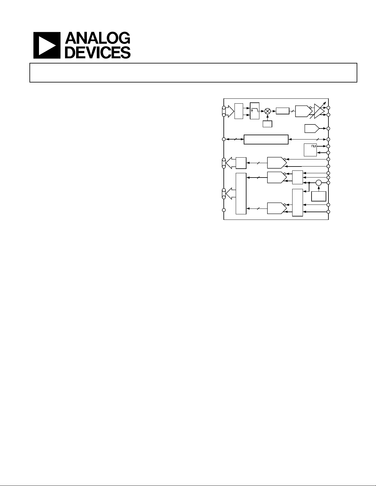
GENERAL DESCRIPTION
The AD9878 is a single-supply, cable modem/set-top box,
mixed-signal front end. The device contains a transmit path
interpolation filter, a complete quadrature digital upconverter,
and a transmit DAC. The receive path contains dual 12-bit
ADCs and a 10-bit ADC. All internally required clocks and an
output system clock are generated by the phase-locked loop
(PLL) from a single crystal oscillator or clock input.
The transmit path interpolation filter provides an upsampling
factor of 16× with an output signal bandwidth up to 4.35 MHz.
Carrier frequencies up to 65 MHz with 26 bits of frequency tuning
resolution can be generated by the direct digital synthesizer
(DDS). The transmit DAC resolution is 12 bits and can run at
sampling rates as high as 232 MSPS. Analog output scaling from
0 dB to 7.5 dB in 0.5 dB steps is available to preserve SNR when
reduced output levels are required.
for Broadband Applications
AD9878
FUNCTIONAL BLOCK DIAGRAM
I
16
TxID[5:0]
SDIO
IF10[4:0]
IF12[11:0]
FLAG[2:1]
Tx
Q
4
CONTROL REGISTERS
MUX
MUX
DDS
10
ADC
12
ADC
12
ADC
Figure 1.
The 12-bit ADCs provide excellent undersampling performance,
allowing this device to typically deliver better than 10 ENOBs
with IF inputs up to 70 MHz. The 12-bit IF ADCs can sample at
rates up to 29 MHz, allowing them to process wideband signals.
The AD9878 includes a programmable ∑-∆ DAC, which can be
used to control an external component such as a variable gain
amplifier (VGA) or a voltage controlled tuner.
The AD9878 also integrates a CA port that enables a host
processor to interface with the AD832x family of programmable
gain amplifier (PGA) cable drivers or industry equivalent via
the MxFE serial port (SPORT).
The AD9878 is available in a 100-lead, LQFP package. The
AD9878 is specified over the extended industrial (−40°C to
+85°C) temperature range.
SINC
12
–1
DAC
Σ-∆
PLL
MUX
CLAMP
MUX
3
Σ
LEVEL
Tx
Σ-∆ OUTPUT
CA PORT
MCLK
OSCIN
IF10 INPUT
IF12B INPUT
VIDEO IN
–
IF12A INPUT
03277-001
Rev. A
Information furnished by Analog Devices is believed to be accurate and reliable.
However, no responsibility is assumed by Analog Devices for its use, nor for any
infringements of patents or other rights of third parties that may result from its use.
Specifications subject to change without notice. No license is granted by implication
or otherwise under any patent or patent rights of Analog Devices. Trademarks and
registered trademarks are the property of their respective owners.
One Technology Way, P.O. Box 9106, Norwood, MA 02062-9106, U.S.A.
Tel: 781.329.4700 www.analog.com
Fax: 781.326.8703 © 2005 Analog Devices, Inc. All rights reserved.
Page 2

AD9878
TABLE OF CONTENTS
Electrical Characteristics ................................................................. 4
Transmit Timing......................................................................... 21
Absolute Maximum Ratings............................................................ 7
Explanation of Test Levels........................................................... 7
Thermal Characteristics .............................................................. 7
ESD Caution.................................................................................. 7
Pin Configuration and Function Descriptions............................. 8
Typical Performance Characteristics ........................................... 10
Terminology .................................................................................... 13
Register Bit Definitions.................................................................. 14
Register 0x00—Initialization .................................................... 15
Register 0x01—Clock Configuration....................................... 15
Register 0x02—Power-Down.................................................... 15
Register 0x03—Flag Control..................................................... 15
Register 0x04—∑-∆ Control Word........................................... 15
Register 0x07—Video Input Configuration............................ 16
Register 0x08—ADC Clock Configuration ............................ 16
Register 0x0C—Die Revision.................................................... 16
Register 0x0D—Tx Frequency Tuning Words LSBs.............. 16
Register 0x0E—DAC Gain Control ......................................... 16
Register 0x0F—Tx Path Configuration................................... 16
Registers 0x10 Through 0x17—Burst Parameter ................... 17
Serial Interface for Register Control............................................ 18
General Operation of the Serial Interface............................... 18
Instruction Byte .......................................................................... 18
Serial Interface Port Pin Descriptions..................................... 18
MSB/LSB Transfers..................................................................... 19
Notes on Serial Port Operation ................................................19
Theory of Operation ...................................................................... 20
Transmit Path.............................................................................. 21
Interpolation Filter..................................................................... 21
Half-Band Filters (HBFs).......................................................... 21
Cascade Integrator Comb (CIC) Filter.................................... 21
Combined Filter Response........................................................ 21
Digital Upconverter ................................................................... 22
Tx Signal Level Considerations................................................ 22
Tx Throughput and Latency..................................................... 23
DAC.............................................................................................. 23
Programming the AD8321/AD8323 or
AD8322/AD8327/AD8238 Cable-Driver Amplifiers............ 23
OSCIN Clock Multiplier ........................................................... 24
Clock and Oscillator Circuitry ................................................. 24
Programmable Clock Output REFCLK .................................. 24
Power-Up Sequence ................................................................... 26
Reset ............................................................................................. 26
Transmit Power-Down .............................................................. 26
∑-∆ Outputs ................................................................................ 27
Receive Path (Rx) ....................................................................... 27
IF10 and IF12 ADC Operation ................................................ 27
ADC Voltage References ........................................................... 29
Video Input ................................................................................. 29
PCB Design Considerations.......................................................... 30
Component Placement .............................................................. 30
Power Planes and Decoupling.................................................. 30
Ground Planes............................................................................ 30
Signal Routing............................................................................. 30
Outline Dimensions....................................................................... 36
Ordering Guide .......................................................................... 36
Data Assembler........................................................................... 21
Rev. A | Page 2 of 36
Page 3

AD9878
REVISION HISTORY
3/05—Rev. 0 to Rev. A
Changed OSCOUT to REFCLK.................................................. Universal
Changes to Electrical Characteristics ........................................................4
Changes to Pin Configuration and Function Descriptions....................8
Changes to ∑-∆ Output Signals (Figure 32)............................................27
Change to ∑-∆ RC Filter (Figure 33) .......................................................27
Changes to Evaluation PCB Schematic (Figure 38 and Figure 39)......31
Updated Outline Dimensions...................................................................36
Changes to Ordering Guide......................................................................36
5/03—Revision 0: Initial Version
Rev. A | Page 3 of 36
Page 4

AD9878
ELECTRICAL CHARACTERISTICS
VAS = 3.3 V ± 5%, VDS = 3.3 V ± 10%, f
= 4.02 kΩ, maximum. Fine gain, 75 Ω DAC load.
R
SET
Table 1.
PARAMETER Temp Test Level Min Typ Max Unit
OSCIN and XTAL CHARACTERISTICS
Frequency Range Full II 3 29 MHz
Duty Cycle 25°C II 35 50 65 %
Input Impedance 25°C III 100||3 MΩ||pF
MCLK Cycle-to-Cycle Jitter (f
derived from PLL) 25°C III 6 ps rms
MCLK
Tx DAC CHARACTERISTICS
Maximum Sample Rate Full II 232 MHz
Resolution N/A N/A 12 Bits
Full-Scale Output Current Full II 4 10 20 mA
Gain Error (Using Internal Reference) 25°C I −2.0 −1 +2.0 % FS
Offset Error 25°C I ±1.0 % FS
Reference Voltage (REFIO Level) 25°C I 1.18 1.23 1.28 V
Differential Nonlinearity (DNL) 25°C III ±2.5 LSB
Integral Nonlinearity (INL) 25°C III ±8 LSB
Output Capacitance 25°C III 5 pF
Phase Noise @ 1 kHz Offset, 42 MHz Carrier 25°C III −110 dBc/Hz
Output Voltage Compliance Range Full II −0.5 +1.5 V
Wideband SFDR
5 MHz Analog Output, I
65 MHz Analog Output, I
= 10 mA Full II 62.4 68 dB
OUT
= 10 mA Full II 50.3 53.5 dB
OUT
Narrow-Band SFDR (±1 MHz Window)
5 MHz Analog Output, I
65 MHz Analog Output, I
= 10 mA Full II 71 74 dB
OUT
= 10 mA Full II 61 64 dB
OUT
Tx MODULATOR CHARACTERISTICS
I/Q Offset Full II 50 55 dB
Pass-Band Amplitude Ripple (f < f
Pass-Band Amplitude Ripple (f < f
Stop-Band Response (f > f
× 3/4) Full II −63 dB
IQCLK
Tx GAIN CONTROL
Gain Step Size 25°C III 0.5 dB
Gain Step Error 25°C III <0.05 dB
Settling Time, 1% (Full-Scale Step) 25°C III 1.8 µs
10-BIT ADC CHARACTERISTICS
Resolution N/A N/A 10 Bits
Maximum Conversion Rate Full II 29 MHz
Pipeline Delay N/A N/A 4.5 ADC cycles
Analog Input
Input Voltage Range Full II 2 V
Differential Input Impedance 25°C III 4||2 kΩ||pF
Full Power Bandwidth 25°C III 90 MHz
Dynamic Performance (AIN = −0.5 dBFS, f = 5 MHz)
Signal-to-Noise and Distortion (SINAD) Full II 57.6 59.7 dB
Effective Number of Bits (ENOB) Full II 9.3 9.6 Bits
Total Harmonic Distortion (THD) Full II −71.1 −63.6 dB
Spurious-Free Dynamic Range (SFDR) Full II 65.7 72.4 dB
Reference Voltage Error, REFT10 to REFB10 (1.0 V) Full I ±4 ±100 mV
= 27 MHz, f
OSCIN
/8) Full II ±0.1 dB
IQCLK
/4) Full II ±0.5 dB
IQCLK
= 216 MHz, f
SYSCLK
= 54 MHz (M = 8), ADC clock derived from OSCIN,
MCLK
PPD
Rev. A | Page 4 of 36
Page 5
AD9878
PARAMETER Temp Test Level Min Typ Max Unit
Dynamic Performance (AIN = −0.5 dBFS, f = 50 MHz)
Signal-to-Noise and Distortion (SINAD) Full II 54.8 57.8 dB
Effective Number of Bits (ENOB) Full II 8.8 9.3 Bits
Total Harmonic Distortion (THD) Full II −63.3 −56.9 dB
Spurious-Free Dynamic Range (SFDR) Full II 56.9 63.7 dB
12-BIT ADC CHARACTERISTICS
Resolution N/A N/A 12 Bits
Maximum Conversion Rate Full II 29 MHz
Pipeline Delay N/A N/A 5.5 ADC cycles
Analog Input
Input Voltage Range Full III 2 V
Differential Input Impedance 25°C III 4||2 kΩ||pF
Aperture Delay 25°C III 2.0 ns
Aperture Jitter 25°C III 1.2 ps rms
Full Power Bandwidth 25°C III 85 MHz
Input Referred Noise 25°C III 75 µV
Reference Voltage Error, REFT12 to REFB12 (1 V) Full I −100 ±16 +100 mV
Dynamic Performance (AIN = −0.5 dBFS, f = 5 MHz)
ADC Sample Clock = OSCIN
Signal-to-Noise and Distortion (SINAD) Full II 61.0 67 dB
Effective Number of Bits (ENOBs) Full II 9.8 10.8 Bits
Signal-to-Noise Ratio (SNR) Full II 64.2 66 dB
Total Harmonic Distortion (THD) Full II −72.7 −61.7 dB
Spurious-Free Dynamic Range (SFDR) Full II 62.8 74.6 dB
ADC Sample Clock = PLL
Signal-to-Noise and Distortion (SINAD) Full II 60.4 64.4 dB
Effective Number of Bits (ENOB) Full II 9.74 10.4 Bits
Signal-to-Noise Ratio (SNR) Full II 62.4 65.1 dB
Total Harmonic Distortion (THD) Full II −72.7 −61.8 dB
Spurious-Free Dynamic Range (SFDR) Full II 62.7 74.6 dB
Dynamic Performance (AIN = −0.5 dBFS, f = 50 MHz)
ADC Sample Clock = OSCIN
Signal-to-Noise and Distortion (SINAD) Full II 61.0 65.2 dB
Effective Number of Bits (ENOB) Full II 9.8 10.5 Bits
Signal-to-Noise Ratio (SNR) Full II 64.2 67.4 dB
Total Harmonic Distortion (THD) Full II −72.8 −61.8 dB
Spurious-Free Dynamic Range (SFDR) Full II 62.8 74.6 dB
Differential Phase 25°C III <0.1 Degrees
Differential Gain 25°C III <1 LSB
VIDEO ADC PERFORMANCE (AIN = −0.5 dBFS, f = 5 MHz)
ADC Sample Clock = OSCIN
Signal-to-Noise and Distortion (SINAD) Full II 46.7 53 dB
Signal-to-Noise Ratio (SNR) Full II 54.3 63.2 Bits
Total Harmonic Distortion (THD) Full II −50.2 −45.9 dB
Spurious-Free Dynamic Range (SFDR) Full II 45.9 50 dB
CHANNEL-TO-CHANNEL ISOLATION
Tx DAC-to-ADC Isolation (5 MHz Analog Output)
Isolation Between Tx and 10-Bit ADC 25°C III >60 dB
Isolation Between Tx and 12-Bit ADCs 25°C III >80 dB
ADC-to-ADC Isolation (AIN = –0.5 dBFS, f = 5 MHz)
Isolation Between IF10 and IF12A/B 25°C III >85 dB
Isolation Between IF12A and IF12B 25°C III >85 dB
PPD
Rev. A | Page 5 of 36
Page 6

AD9878
PARAMETER Temp Test Level Min Typ Max Unit
TIMING CHARACTERISTICS (10 pF Load)
Wake-Up Time N/A N/A 200 t
Minimum RESET Pulse Width Low, tRL
N/A N/A 5 t
Digital Output Rise/Fall Time Full II 2.8 4 ns
Tx/Rx Interface
MCLK Frequency, f
Full II 58 MHz
MCLK
TxSYNC/TxIQ Setup Time, tSU Full II 3 ns
TxSYNC/TxIQ Hold Time, tHU Full II 3 ns
MCLK Rising Edge to RxSYNC Valid Delay, tMD Full II 0 1.0 ns
REFCLK Rising or Falling Edge to
RxSYNC Valid Delay, t
OD
Full II
/
t
OSCIN
4 − 2.0
t
OSCIN
/
4 + 3.0
REFCLK Edge to MCLK Falling Edge, tEE Full II −1.0 +1.0 ns
SERIAL CONTROL BUS
Maximum SCLK Frequency, f
Minimum Clock Pulse Width High, t
Minimum Clock Pulse Width Low, t
Full II 15 MHz
SCLK
Full II 30 ns
PWH
Full II 30 ns
PWL
Maximum Clock Rise/Fall Time Full II 1 µs
Minimum Data/Chip-Select Setup Time, tDS Full II 25 ns
Minimum Data Hold Time, tDH Full II 0 ns
Maximum Data Valid Time, tDV Full II 30 ns
CMOS LOGIC INPUTS
Logic 1 Voltage 25°C II V
− 0.7 V
DRVDD
Logic 0 Voltage 25°C II 0.4 V
Logic 1 Current 25°C II 12 µA
Logic 0 Current 25°C II 12 µA
Input Capacitance 25°C III 3 pF
CMOS LOGIC OUTPUTS (1 mA Load)
Logic 1 Voltage 25°C II V
− 0.6 V
DRVDD
Logic 0 Voltage 25°C II 0.4 V
POWER SUPPLY
Supply Current, IS (Full Operation) 25°C II 184 204 mA
Analog Supply Current, IAS 25°C III 105 115 mA
Digital Supply Current, IDS 25°C III 79 89 mA
Supply Current, IS
Standby (PWRDN Pin Active, IAS + IDS )
25°C II 124 137 mA
Full Power-Down (Register 0x02 = 0xFF) 25°C II 46 52 mA
Power-Down Tx Path (Register 0x02 = 0x60) 25°C III 124 mA
Power-Down IF12 Rx Path (Register 0x02 = 0x1B) 25°C III 131 159 mA
Power Supply Rejection (Differential Signal)
Tx DAC 25°C III <0.25 % FS
10-Bit ADC 25°C III <0.0001 % FS
12-Bit ADC 25°C III <0.0004 % FS
ns
MCLK
MCLK
cycles
cycles
Rev. A | Page 6 of 36
Page 7
AD9878
ABSOLUTE MAXIMUM RATINGS
Table 2.
Parameter Rating
Power Supply (V
Digital Output Current 5 mA
Digital Inputs −0.3 V to V
Analog Inputs −0.3 V to V
Operating Temperature −40°C to +85°C
Maximum Junction Temperature 150°C
Storage Temperature −65°C to +150°C
Lead Temperature (Soldering, 10 sec) 300°C
AVDD
, V
DVDD
, V
) 3.9 V
DRVDD
DRVDD
AVDD
+ 0.3 V
+ 0.3 V
Stresses above those listed under Absolute Maximum Ratings
may cause permanent damage to the device. This is a stress
rating only; functional operation of the device at these or any
other condition s above those indicated in the operational
section of this specification is not implied. Exposure to absolute
maximum rating conditions for extended periods may affect
device reliability.
EXPLANATION OF TEST LEVELS
I. Devices are 100% production tested at 25°C and guaranteed
II. Parameter is guaranteed by design and/or characterization
III. Parameter is a typical value only.
N/A. Test level definition is not applicable.
THERMAL CHARACTERISTICS
Thermal resistance of 100-lead LQFP: θJA = 40.5°C/W
by design and characterization testing for extended industrial
operating temperature range (−40°C to +85°C).
testing.
ESD CAUTION
ESD (electrostatic discharge) sensitive device. Electrostatic charges as high as 4000 V readily accumulate on
the human body and test equipment and can discharge without detection. Although this product features
proprietary ESD protection circuitry, permanent damage may occur on devices subjected to high energy
electrostatic discharges. Therefore, proper ESD precautions are recommended to avoid performance
degradation or loss of functionality.
Rev. A | Page 7 of 36
Page 8
AD9878
PIN CONFIGURATION AND FUNCTION DESCRIPTIONS
AVDD
AGND
VIDEO IN
AGND
IF12A+
IF12A–
AGND
AVDD
REFT12A
REFB12AAVDD
AGND
IF12B+
IF12B–
AGND
AVDD
39
40
41CS42
SCLK
DVDD
DGND
DRGND
DRVDD
(MSB) IF12(11)
IF12(10)
IF12(9)
IF12(8)
IF12(7)
IF12(6)
IF12(5)
IF12(4)
IF12(3)
IF12(2)
IF12(1)
IF12(0)
(MSB) IF10(4)
IF10(3)
IF10(2)
IF10(1)
IF10(0)
RxSYNC
DRGND
DRVDD
MCLK
DVDD
DGND
100
99 98 97 96 95 94 93 92 91 90 89 88 87 86 85 84 83 82 81 80 79 78 77
1
2
3
4
5
6
7
8
9
10
11
12
13
14
15
16
17
18
19
20
21
22
23
24
25
26
27
TxSYNC
(MSB) TxIQ(5)
TxIQ(4)28TxIQ(3)29TxIQ(2)30TxIQ(1)31TxIQ(0)
32
33
34
DVDD
35
DGND
AD9878
TOP VIEW
(Not to Scale)
36
37
DVDD
DGND
38
RESET
PROFILE
Figure 2. Pin Configuration
REFT12B
43
REFB12BAVDD
44
SDIO
SDO
AGND
45
46
DGNDTx
AVDD10
47
DVDDTx
AGND10
PWRDN
48
IF10+
49
REFIO
IF10–
FSADJ
AGND
76
75
74
73
72
71
70
69
68
67
66
65
64
63
62
61
60
59
58
57
56
55
54
53
52
51
50
AGNDTx
REFT10
REFB10
AGND10
AVDD10
DRVDD
DRGND
REFCLK
SIGDELT
FLAG1
FLAG2
CA_EN
CA_DATA
CA_CLK
DVDDOSC
OSCIN
XTAL
DGNDOSC
AGNDPLL
PLLFILT
AVDDPLL
DVDDPLL
DGNDPLL
AVDDTx
Tx+
Tx–
03277-002
Table 3. Pin Function Descriptions
Pin No. Mnemonic Descriptions
1, 21, 70 DRGND Pin Driver Digital Ground
2, 22, 71 DRVDD Pin Driver Digital 3.3 V Supply
3 (MSB) IF12(11) 12-Bit ADC Digital Ouput
4 to 14 IF12[10:0] 12-Bit ADC Digital Ouput
15 (MSB) IF10(4) 10-Bit ADC Digital Ouput
16 to 19 IF10[3:0] 10-Bit ADC Digital Ouput
20 RxSYNC Sync Output, 10-Bit and 12-Bit ADCs
23 MCLK Master Clock Output
24, 33, 35, 39 DVDD Digital 3.3 V Supply
25, 34, 36, 40 DGND Digital Ground
26 TxSYNC Sync Input for Transmit Port
27 (MSB) TxIQ(5) Digital Input for Transmit Port
28 to 32 TxIQ[4:0] Digital Input for Transmit Port
37 PROFILE Profile Selection Input
38
RESET
Chip Reset Input
41 SCLK SPORT Clock
42
CS
SPORT Chip Select
43 SDIO SPORT Data I/O
Rev. A | Page 8 of 36
Page 9

AD9878
Pin No. Mnemonic Descriptions
44 SDO SPORT Data Output
45 DGNDTx Tx Path Digital Ground
46 DVDDTx Tx Path Digital 3.3 V Supply
47
48 REFIO TxDAC Decoupling (to AGND)
49 FSADJ DAC Output Adjust (External Resistor)
50 AGNDTx Tx Path Analog Ground
51, 52 Tx−, Tx+ Tx Path Complementary Outputs
53 AVDDTx Tx Path Analog 3.3 V Supply
54 DGNDPLL PLL Digital Ground
55 DVDDPLL PLL Digital 3.3 V Supply
56 AVDDPLL PLL Analog 3.3 V Supply
57 PLLFILT PLL Loop Filter Connection
58 AGNDPLL PLL Analog Ground
59 DGNDOSC Oscillator Digital Ground
60 XTAL Crystal Oscillator Inverted Output
61 OSCIN Oscillator Clock Input
62 DVDDOSC Oscillator Digital 3.3 V Supply
63 CA_CLK Serial Clock-to-Cable Driver
64 CA_DATA Serial Data-to-Cable Driver
65
66, 67 FLAG[2:1] Programmable Flag Outputs
68 SIGDELT ∑-∆ DAC Output
69 REFCLK Reference Clock Output
72, 80 AVDD10 10-Bit ADC Analog 3.3 V Supply
73, 79 AGND10 10-Bit ADC Analog Ground
74 REFB10 10-Bit ADC Reference Decoupling Node
75 REFT10 10-Bit ADC Reference Decoupling Node
76, 81, 86, 89, 94,
97, 99
77, 78 IF10−, IF10+ Differential Input to 10-bit ADC
82, 85, 90, 93, 100 AVDD 12-Bit ADC Analog 3.3 V Supply
83 REFB12B ADC12B Reference Decoupling Node
84 REFT12B ADC12B Reference Decoupling Node
87, 88 IF12B−, IF12B+ Differential Input to ADC12B
91 REFB12A ADC12A Reference Decoupling Node
92 REFT12A ADC12A Reference Decoupling Node
95, 96 IF12A−, IF12A+ Differential Input to ADC12A
98 VIDEO IN Video Clamp Input
PWRDN
CA_EN
AGND 12-Bit ADC Analog Ground
Power-Down Transmit Path
Serial Enable-to-Cable Driver
Rev. A | Page 9 of 36
Page 10
AD9878
TYPICAL PERFORMANCE CHARACTERISTICS
0
–10
–20
–30
–40
–50
–60
MAGNITUDE (dB)
–70
–80
–90
–100
024681012141618
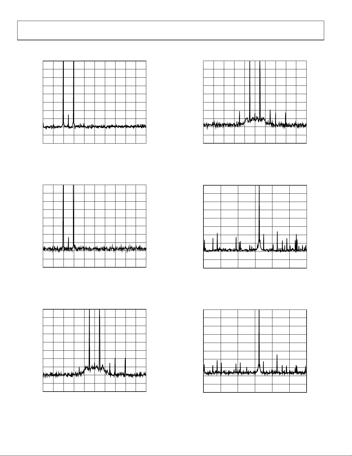
Figure 3. Dual-Sideband Spectral Plot, f
R
SET
= 10 kΩ (I
FREQUENCY (MHz)
= 4 mA), RBW = 1 kHz
OUT
C
= 5 MHz, f = 1 MHz,
03277-022
20
0
–10
–20
–30
–40
–50
–60
MAGNITUDE (dB)
–70
–80
–90
–100
55 57 59 61 63 65 67 69 71 73
Figure 6. Dual-Sideband Spectral Plot, f
R
SET
= 4 kΩ (I
FREQUENCY (MHz)
= 65 MHz, f = 1 MHz,
= 10 mA), RBW = 1 kHz
OUT
C
03277-025
75
0
–10
–20
–30
–40
–50
–60
MAGNITUDE (dB)
–70
–80
–90
–100
024681012141618
Figure 4. Dual-Sideband Spectral Plot, f
R
SET
0
–10
–20
–30
–40
–50
–60
MAGNITUDE (dB)
–70
–80
–90
–100
55 57 59 61 63 65 67 69 70 73
Figure 5. Dual-Sideband Spectral Plot, f
f = 1 MHz, R
= 4 kΩ (I
= 10 kΩ (I
SET
FREQUENCY (MHz)
= 5 MHz, f = 1 MHz,
= 10 mA), RBW = 1 kHz
OUT
FREQUENCY (MHz)
OUT
C
= 4 mA), RBW = 1 kHz
= 65 MHz,
C
20
75
03277-023
03277-024
0
–10
–20
–30
–40
–50
–60
MAGNITUDE (dB)
–70
–80
–90
–100
0 20406080100
Figure 7. Single Sideband @ 65 MHz, f
f = 1 MHz, R
0
–10
–20
–30
–40
–50
–60
MAGNITUDE (dB)
–70
–80
–90
–100
0 20406080100
Figure 8. Single Sideband @ 65 MHz, f
f = 1 MHz, R
FREQUENCY (MHz)
= 10 kΩ (I
SET
FREQUENCY (MHz)
= 4 kΩ (I
SET
= 66 MHz,
= 4 mA), RBW = 2 kHz
OUT
= 10 mA), RBW = 2 kHz
OUT
C
= 66 MHz,
C
120
120
03277-026
03277-027
Rev. A | Page 10 of 36
Page 11
AD9878
0
–10
–20
–30
–40
–50
–60
MAGNITUDE (dB)
–70
–80
–90
–100
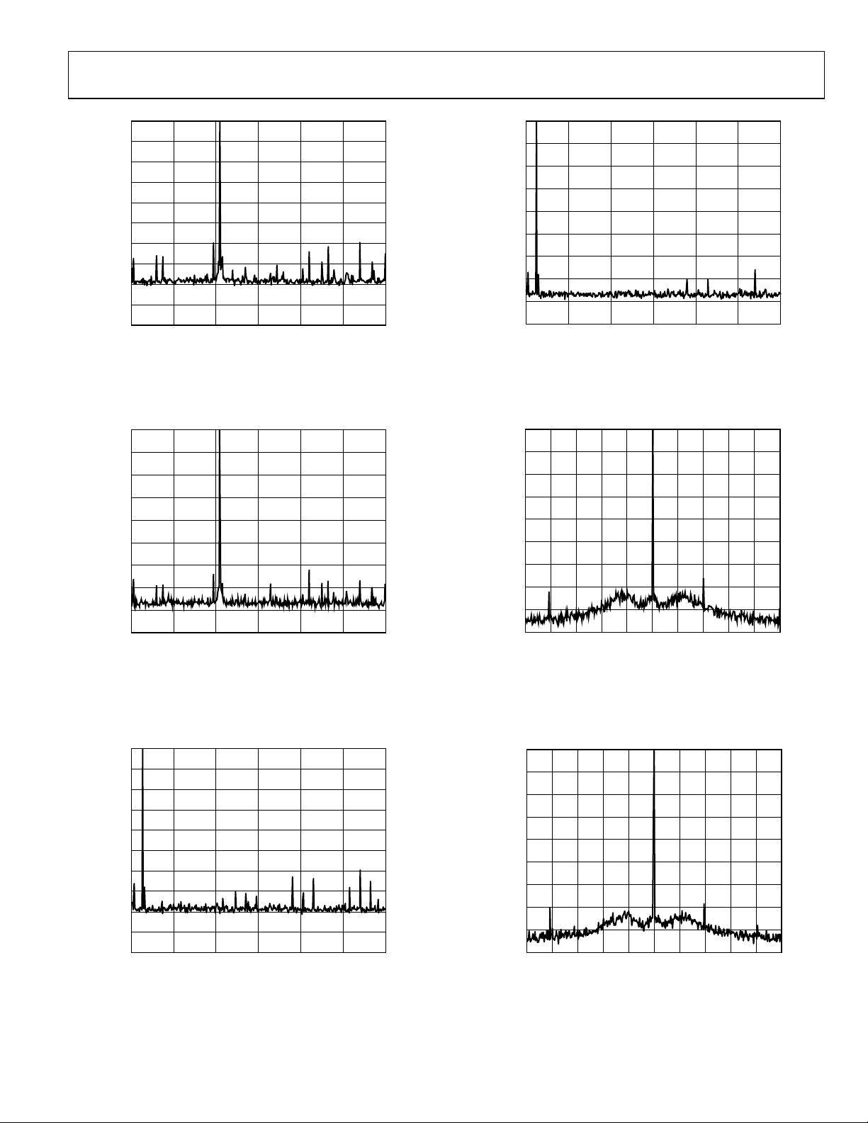
0 20406080100
Figure 9. Single Sideband @ 42 MHz, f
f = 1 MHz, R
FREQUENCY (MHz)
= 10 kΩ (I
SET
= 43 MHz,
= 4 mA), RBW = 2 kHz
OUT
C
03277-028
120
0
–10
–20
–30
–40
–50
–60
MAGNITUDE (dB)
–70
–80
–90
0 20406080100
Figure 12. Single Sideband @ 5 MHz, f
f = 1 MHz, R
FREQUENCY (MHz)
= 4 kΩ (I
SET
= 6 MHz,
= 10 mA), RBW = 2 kHz
OUT
C
03277-031
120
0
–10
–20
–30
–40
–50
–60
MAGNITUDE (dB)
–70
–80
–90
0 20406080100
Figure 10. Single Sideband @ 42 MHz, f
f = 1 MHz, R
0
–10
–20
–30
–40
–50
–60
MAGNITUDE (dB)
–70
–80
–90
–100
0 20406080100
Figure 11. Single Sideband @ 5 MHz, f
f = 1 MHz, R
FREQUENCY (MHz)
= 4 kΩ (I
SET
FREQUENCY (MHz)
= 10 kΩ (I
SET
= 43 MHz,
= 10 mA), RBW = 2 kHz
OUT
= 4 mA), RBW = 2 kHz
OUT
C
= 6 MHz,
C
120
120
03277-029
03277-030
0
–10
–20
–30
–40
–50
–60
MAGNITUDE (dB)
–70
–80
–90
–2.5 –2.0 –1.5 –1.0 –0.5 0 0.5 1.0 1.5 2.0
Figure 13. Single Sideband @ 65 MHz, f
f = 1 MHz, R
0
–10
–20
–30
–40
–50
–60
MAGNITUDE (dB)
–70
–80
–90
–2.5 –2.0 –1.5 –1.0 –0.5 0 0.5 1.0 1.5 2.0
Figure 14. Single Sideband @ 65 MHz, f
f = 1 MHz, R
FREQUENCY (MHz)
= 10 kΩ (I
SET
FREQUENCY (MHz)
= 4 kΩ (I
SET
= 66 MHz,
= 4 mA), RBW = 500 Hz
OUT
= 10 mA), RBW = 500 Hz
OUT
C
= 66 MHz,
C
03277-032
2.5
03277-033
2.5
Rev. A | Page 11 of 36
Page 12

AD9878
0
–10
–20
–30
–40
–50
–60
MAGNITUDE (dB)
–70
–80
–90
–100
–50 –40 –30 –20 –10 0 10 20 30 40
FREQUENCY (MHz)
Figure 15. Single Sideband @ 65 MHz, f
f = 1 MHz, R
= 10 kΩ (I
SET
= 4 mA), RBW = 50 Hz
OUT
= 66 MHz,
C
50
03277-034
0
–10
–20
–30
–40
–50
MAGNITUDE (dB)
–60
–70
–80
0 5 10 15 20 25 30 35 40 45 50
FREQUENCY (MHz)
Figure 17. 16-QAM @ 42 MHz Spectral Plot, RBW = 1 kHz
03277-036
0
–10
–20
–30
–40
–50
–60
MAGNITUDE (dB)
–70
–80
–90
–100
–2.5 –2.0 –1.5 –1.0 –0.5 0 0.5 1.0 1.5 2.0 2.5
Figure 16. Single Sideband @ 65 MHz, f
f = 1 MHz, R
FREQUENCY (MHz)
= 10 kΩ (I
SET
= 66 MHz,
= 4 mA), RBW = 10 Hz
OUT
C
03277-035
0
–10
–20
–30
–40
–50
MAGNITUDE (dB)
–60
–70
–80
0 5 10 15 20 25 30 35 40 45 50
FREQUENCY (MHz)
Figure 18. 16-QAM @ 5 MHz Spectral Plot, RBW = 1 kHz
03277-037
Rev. A | Page 12 of 36
Page 13

AD9878
(
)
−
=
TERMINOLOGY
Differential Nonlinearity Error (DNL, No Missing Codes)
An ideal converter exhibits code transitions that are exactly 1 LSB
apart. DNL is the deviation from this ideal value. No missing
codes indicates that all of the ADC codes must be present over
all operating ranges.
Aperture Delay
The aperture delay is a measure of the sample-and-hold amplifier
(SHA) performance that specifies the time delay between the
rising edge of the sampling clock input and when the input
signal is held for conversion.
Integral Nonlinearity Error (INL)
Linearity error refers to the deviation of each individual code from
a line drawn from negative full scale through positive full scale.
The point used as negative full scale occurs ½ LSB before the first
code transition. Positive full scale is defined as a level 1½ LSB
beyond the last code transition. The deviation is measured from
the middle of each code to the true straight line.
Phase Noise
Single-sideband, phase-noise power is specified relative to the
carrier (dBc/Hz) at a given frequency offset (1 kHz) from the
carrier. Phase noise can be measured directly in single-tone
transmit mode with a spectrum analyzer that supports noise
marker measurements. It detects the relative power between
the carrier and the offset (1 kHz) sideband noise and takes
the resolution bandwidth (RBW) into account by subtracting
10 × log(RBW). It also adds a correction factor that compensates
for the implementation of the resolution bandwidth, log display,
and detector characteristic.
Output Compliance Range
The range of allowable voltage at the output of a current-output
DAC. Operation beyond the maximum compliance limits can
cause either output stage saturation or breakdown, resulting in
nonlinear performance.
Aperture Jitter
Aperture jitter is the variation in aperture delay for successive
samples and is manifested as noise on the input to the ADC.
Input Referred Noise
The rms output noise is measured using histogram techniques.
The standard deviation of the ADC output codes is calculated
in LSB, and converted to an equivalent voltage. This results in a
noise figure that can be directly referred to the input of the MxFE.
Signal-to-Noise and Distortion (SINAD) Ratio
SINAD is the ratio of the rms value of the measured input signal
to the rms sum of other spectral components below the Nyquist
frequency, including harmonics, but excluding dc. The value for
SINAD is expressed in decibels.
Effective Number of Bits (ENOB)
For a sine wave, SINAD can be expressed in terms of the number
of bits. Using the following formula, it is possible to get a measure
of performance expressed as N, the effective number of bits:
SINADN
Thus, the effective number of bits for a device for sine wave
inputs at a given input frequency can be calculated directly
from its measured SINAD.
02.6dB76.1
Spurious-Free Dynamic Range (SFDR)
The difference, in dB, between the rms amplitude of the DAC
output signal (or ADC input signal) and the peak spurious signal
over the specified bandwidth (Nyquist bandwidth, unless
otherwise noted).
Pipeline Delay (Latency)
The number of clock cycles between conversion initiation and
the associated output data being made available.
Offset Error
The first code transition should occur at an analog value ½ LSB
above negative full scale. Offset error is defined as the deviation
of the actual transition from that point.
Gain Error
The first code transition should occur at an analog value ½ LSB
above negative full scale. The last transition should occur for an
analog value 1½ LSB below the nominal full scale. Gain error
is the deviation of the actual difference between first and last
code transitions and the ideal difference between first and last
code transitions.
Rev. A | Page 13 of 36
Signal-to-Noise Ratio (SNR)
SNR is the ratio of the rms value of the measured input signal
to the rms sum of other spectral components below the Nyquist
frequency, excluding harmonics and dc. The value for SNR is
expressed in decibels.
Total Harmonic Distortion (THD)
THD is the ratio of the rms sum of the first six harmonic
components to the rms value of the measured input signal.
It is expressed as a percentage, or in decibels.
Power Supply Rejection
Power supply rejection specifies the converter’s maximum fullscale change when the supplies are varied from nominal to
minimum or maximum specified voltages.
Channel-to-Channel Isolation (Crosstalk)
In an ideal multichannel system, the signal in one channel does
not influence the signal level of another channel. The channelto-channel isolation specification is a measure of the change
that occurs in a grounded channel as a full-scale signal is
applied to another channel.
Page 14

AD9878
REGISTER BIT DEFINITIONS
Table 4. Register Map
Address
(Hex) Bit 7 Bit 6 Bit 5 Bit 4 Bit 3 Bit 2 Bit 1 Bit 0
0x00
0x01
SDIO
bidirectional
PLL lock
LSB
first
Reset OSCIN multiplier M[4:0]
MCLK divider R[5:0]
0x08 Read/write
0x00 Read/write
detect
0x02
0x03
Power down
PLL
Power
down
DAC
Tx
Power
down
digital
Tx
Video
input
Power
down
ADC12A
Flag 2
Power down
ADC12B
Power
down
ADC10
Power
down
reference
ADC12A
Flag 1
Power
down
reference
ADC12B
Flag 0
enable
into
ADC12B
0x04 MSB/Flag 0 ∑-∆ output control word [7:0] 0x00 Read/write
0x05
0x06
0x07
Video input
Clamp level for video input [6:0] 0x00 Read/write
enable
0x08
0x09
0x0A
0x0B
0x0C
0x0D
0x0E
0x0F
ADC clocked
directly from
OSCIN
Rx port
fast
edge
rate
Power
down
RxSYNC
generator
Power down
reference
ADC10
Tx frequency tuning word
profile 1 LSB [1:0]
Tx path
select
Profile 1
Tx path
AD8321/AD8323
gain control
mode
Send
ADC12A
data only
Send
ADC12B
data only
Version [3:0] 0x00 Read/write
Tx frequency tuning
word profile 0 LSBs [1:0]
DAC fine gain control [3:0] 0x00 Read/write
Tx
path
bypass
–1
sinc
Tx path
spectral
inversion
Tx path
transmit
single
tone
filter
0x10 Tx Path Frequency Tuning Word Profile 0 [9:2] 0x00 Read/write
0x11 Tx Path Frequency Tuning Word Profile 0 [17:10] 0x00 Read/write
0x12 Tx Path Frequency Tuning Word Profile 0 [25:18] 0x00 Read/write
0x13
Cable-driver amplifier,
Coarse Gain Control Profile 0 [7:4]
Cable-driver amplifier,
Fine Gain Control Profile 0 [3:0]
0x14 Tx Path Frequency Tuning Word Profile 1 [9:2] 0x00 Read/write
0x15 Tx Path Frequency Tuning Word Profile 1 [17:10] 0x00 Read/write
0x16 Tx Path Frequency Tuning Word Profile 1 [25:18] 0x00 Read/write
0x17
Cable-driver amplifier,
Coarse Gain Control Profile 1 [7:4]
Cable-driver amplifier,
Fine Gain Control Profile 1 [3:0]
Default
(Hex) Type
0x00 Read/write
0x00 Read/write
0x00 Read/write
0x00 Read only
0x80 Read/write
0x00 Read/write
0x00 Read/write
0x00 Read/write
0x00 Read/write
0x00 Read/write
0x00 Read/write
0x00 Read/write
Rev. A | Page 14 of 36
Page 15

AD9878
REGISTER 0x00—INITIALIZATION
Bits 0 to 4: OSCIN Multiplier
This register field is used to program the on-chip clock
multiplier that generates the chip’s high frequency system clock,
f
. For example, to multiply the external crystal clock f
SYSCLK
OSCIN
by 16, program Register 0x00, Bits 4:0, to 0x10. The default
clock multiplier value, M, is 0x08. Valid entries range from 1 to
31. When M is set to 1, the PLL is disabled and internal clocks
are derived directly from OSCIN. The PLL requires 200 MCLK
cycles to regain frequency lock after a change in M. After the
recapture time of the PLL, the frequency of f
SYSCLK
is stable.
Bit 5: Reset
Writing 1 to this bit resets the registers to their default values
and restarts the chip. The reset bit always reads back 0. The bits
in Register 0x00 are not affected by this software reset. However,
a low level at the
pin forces all registers, including all
RESET
bits in Register 0x00, to their default states.
Bit 6: LSB First
Active high indicates SPI serial port access of instruction byte and
data registers is LSB first. Default low indicates MSB-first format.
Bit 7: SDIO Bidirectional
Active high configures the serial port as a 3-signal port with
the SDIO pin used as a bidirectional input/output pin. Default
low indicates that the serial port uses four signals with SDIO
configured as an input and SDO configured as an output.
REGISTER 0x01—CLOCK CONFIGURATION
Bits [5:0]: MCLK Divider
This register determines the output clock on the REFCLK pin.
At default 0 (R = 0), REFCLK provides a buffered version of the
OSCIN clock signal for other chips. The register can also be used
to divide the chip’s master clock f
by R, where R is an integer
MCLK
between 2 and 63. The generated reference clock on REFCLK pin
can be used for external frequency controlled devices.
Bit 7: PLL Lock Detect
When this bit is set low, the REFCLK pin functions in its
default mode and provides an output clock with frequency
f
/R, as described above. If this bit is set to 1, the REFCLK pin
MCKL
is configured to indicate whether the PLL is locked to f
OSCIN
. In
this mode, the REFCLK pin should be low-pass filtered with an
RC filter of 1.0 kΩ and 0.1 µF. A low output on REFCLK indicates
that the PLL has achieved lock with f
OSCIN
.
REGISTER 0x02—POWER-DOWN
Unused sections of the chip can be powered down when the
corresponding bits are set high. This register has a default value
of 0x00, all sections active.
Bit 0: Power Down ADC12B Voltage Reference
Active high powers down the voltage reference circuit
for ADC12B.
Bit 1: Power Down ADC12A Voltage Reference
Active high powers down the voltage reference circuit for
the ADC12A.
Bit 2: Power Down ADC10
Active high powers down the 10-bit ADC.
Bit 3: Power Down ADC12B
Active high powers down the ADC12B.
Bit 4: Power Down ADC12A
Active high powers down the ADC12A.
Bit 5: Power Down Tx
Active high powers down the digital transmit section of the
chip, similar to the function of the
PWRDN
pin.
Bit 6: Power Down DAC Tx
Active high powers down the DAC.
Bit 7: Power Down PLL
Active high powers down the OSCIN multiplier.
REGISTER 0x03—FLAG CONTROL
Bit 0: Flag 0 Enable
When this bit is active high, the SIGDELT pin maintains a fixed
logic level determined directly by the MSB of the ∑-∆ control
word of Register 0x04.
Bit 1: Flag 1
The logic level of this bit is applied at the FLAG1 pin.
Bit 4: Flag 2
The logic level of this bit is applied at the FLAG2 pin.
Bit 5: Video Input into ADC12B
If the video input is enabled, setting this bit high sends the
signal applied to the VIDEO IN pin to the ADC12B. Otherwise,
the signal applied to the VIDEO IN pin is sent to the ADC12A.
REGISTER 0x04—∑-∆ CONTROL WORD
Bits [7:0]: ∑-∆ Control Word
The ∑-∆ control word is 8 bits wide and controls the duty cycle
of the digital output on the SIGDELT pin. Changes to the ∑-∆
control word take effect immediately for every register write.
∑-∆ output control words have a default value of 0. The control
words are in straight binary format, with 0x00 corresponding to
the bottom of scale or 0% duty cycle, and 0xFF corresponding
to the top of scale or near 100% duty cycle.
Bit 7: Flag 0 (∑-∆ Control Word MSB)
When the Flag 0 enable bit (Register 0x03, Bit 0) is set, the logic
level of this bit appears on the output of the SIGDELT pin.
Rev. A | Page 15 of 36
Page 16

AD9878
(
)
()(
)
[
]
ω+ω=
(
[
]
ω−ω=
REGISTER 0x07—VIDEO INPUT CONFIGURATION
Bits [6:0]: Clamp Level Control Value
The 7-bit clamp-level control value is used to set an offset to the
automatic clamp-level control loop. The actual ADC output has a
clamp-level offset equal to 16 times the clamp level control value.
16-- xValueControlLevelClampOffsetLevelClamp =
The default value for the clamp-level control value is 0x20. This
results in an ADC output clamp-level offset of 512 LSBs. The
valid programming range for the clamp-level control value is
0x16 to 0x127.
Bit 7: Video Input Enable
This bit enables the video input. In default with Bit 7 = 0, both
IF12 ADCs are connected to IF inputs. If the video input is
enabled by setting bit 7 = 1, the video input will be connected to
the IF12 ADC selected by REG 0x03, Bit 6.
REGISTER 0x08—ADC CLOCK CONFIGURATION
Bit 0: Send ADC12B Data Only
When this bit is set high, the device enters a nonmultiplexed
mode, and only the data from the ADC12B is sent to the
IF[11:0] digital output port.
Bit 1: Send ADC12A Data Only
When this bit is set high, the device enters a nonmultiplexed
mode, and only the data from the ADC12A is sent to the
IF[11:0] digital output port.
If both the send ADC12B data only and send ADC12A data
only register bits are set high, the device sends both ADC12A
and ADC12B data in the default multiplexed mode.
Bit 3: Power Down ADC10 Voltage Reference
Active high powers down the voltage reference circuit for
the ADC10.
Bit 4: Power Down RxSYNC Generator
Setting this bit to 1 powers down the 10-bit ADC’s sampling
clock and makes the RxSYNC output pin stay low. It can be
used for additional power saving on top of the power-down
selections in Register 0x02.
Bit 5: Rx PORT Fast Edge Rate
Setting this bit to 1 increases the output drive strength of all digital
output pins, except MCLK, REFCLK, SIGDELT, and
FLAG[2:1]. These pins always have high output drive capability.
Bit 7: ADC Clocked Directly from OSCIN
When set high, the ADC sampling clock is derived directly from
the input clock at OSCIN. In this mode, the clock supplied to the
OSCIN pin should originate from an external crystal or low jitter
crystal oscillator. When this bit is low, the ADC sampling clock
is derived from the internal PLL and the frequency of the clock
is equal to f
OSCIN
× M/8.
REGISTER 0x0C—DIE REVISION
Bits [3:0]: Version
The die version of the chip can be read from this register.
REGISTER 0x0D—Tx FREQUENCY TUNING WORDS LSBs
This register accommodates the 2 LSBs for each frequency tuning
word (FTW). See the Registers 0x10 Through 0x17—
Burst Parameter section.
REGISTER 0x0E—DAC GAIN CONTROL
This register allows the user to program the DAC gain if the
Tx Gain Control Select Bit 3 in Register 0x0F is set to 0.
Table 5. DAC Gain Control
Bits [3:0] DAC Gain (dB)
0000 0.0 (default)
0001 0.5
0010 1.0
0011 1.5
… …
1110 7.0
1111 7.5
REGISTER 0x0F—Tx PATH CONFIGURATION
Bit 0: Single Tone Tx Mode
Active high configures the AD9878 for single-tone applications
(e.g., FSK). The AD9878 supplies a single frequency output, as
determined by the FTW selected by the active profile. In this
mode, the TxIQ input data pins are ignored, but should be tied
to a valid logic voltage level. Default value is 0x00 (inactive).
Bit 1: Spectral Inversion Tx
When set to 1, inverted modulation is performed:
.sincos_ tQtIOUTMODULATOR
Default is Logic 0, noninverted modulation:
()
Bit 2: Bypass Inv Sinc Tx Filter
Active high configures the AD9878 to bypass the sin(x)/x compensation filter. Default value is 0x00 (inverse sinc filter enabled).
Bit 3: CA Interface Mode Select
This bit changes the format of the AD9878 3-wire CA interface to
a format in which the AD9878 digitally interfaces to external
variable gain amplifiers. This is accomplished by changing
the interpretation of the bits in Register 0x13, Register 0x17,
Register 0x1B, and Register 0x1F. See the Cable-Driver Gain
Control section for more detail.
)
.sincos_ tQtIOUTMODULATOR
Rev. A | Page 16 of 36
Page 17

AD9878
(
+
=
(
(
)
+
=
Setting this bit to 0 (default) configures the serial interface to be
compatible with AD8321/AD8323/AD8328 variable cable gain
amplifiers. Setting this bit to 1 configures the serial interface to be
compatible with AD8322/AD8327 variable cable gain amplifiers.
Bit 5: Profile Select
The AD9878 quadrature digital upconverter can store two
preconfigured modulation modes, called profiles. Each profile
defines a transmit FTW, cable-driver amplifier gain setting, and
DAC gain setting. The profile select bit or PROFILE pin programs
the current register profile to be used. If the PROFILE pin is used
to switch between profiles, the profile select bit should be set to 0
and tied low.
REGISTERS 0x10 THROUGH 0x17— BURST PARAMETER
Tx Frequency Tuning Words
The FTW determines the DDS-generated carrier frequency (fC)
and is formed via a concatenation of register addresses.
The 26-bit FTW is spread over four register addresses. Bit 25 is
the MSB, and Bit 0 is the LSB. The carrier frequency equation is
as follows:
()
fFTWf ×=
SYSCLKC
Where 2000x0and, <×= FTWfMf
Changes to FTW bytes take effect immediately.
Cable-Driver Gain Control
The AD9878 has a 3-pin interface to the AD832x family of
programmable gain cable-driver amplifiers. This allows direct
control of the cable driver’s gain through the AD9878. In its
default mode, the complete 8-bit register value is transmitted
over the 3-wire cable amplifier (CA) interface.
If Bit 3 of Register 0x0F is set high, Bits [7:4] of Register 0x13
and Register 0x17 determine the 8-bit word sent over the CA
interface, according to the specifications in Table 6. Bits [3:0] of
Register 0x13 and Register 0x17 determine the fine gain setting
of the DAC output, according to specifications in Table 7.
26
2
OSCINSYSCLK
.
Table 6. Cable-Driver Gain Control
Bits [7:4] CA Interface Transmit Word
0000 0000 0000 (default)
0001 0000 0001
0010 0000 0010
0011 0000 0100
0100 0000 1000
0101 0001 0000
0110 0010 0000
0111 0100 0000
1000 1000 0000
Table 7. DAC Output Fine Gain Setting
Bits [3:0] DAC Fine Gain (dB)
0000 0.0 (default)
0001 0.5
0010 1.0
0011 1.5
… …
1110 7.0
1111 7.5
New data is automatically sent over the 3-wire CA interface
(and DAC gain adjust) whenever the value of the active gain
control register changes or a new profile is selected. The default
value is 0x00 (lowest gain).
The formula for the combined output-level calculation of
AD9878 fine gain and AD8327 or AD8322 coarse gain is:
8327
8322
()
09878
()
09878
()
coarsefineVV
)
coarsefineVV
192
−+
142
−+
)
where:
fine is the decimal value of Bits [3:0].
coarse is the decimal value of Bits [7:4].
V
is the level at AD9878 output in dBmV for fine = 0.
9878(0)
V
is the level at output of AD8327 in dBmV.
8327
V
is the level at output of AD8322 in dBmV.
8322
Rev. A | Page 17 of 36
Page 18

AD9878
SERIAL INTERFACE FOR REGISTER CONTROL
The AD9878 serial port is a flexible, synchronous, serial
communications port that allows easy interface to many
industry-standard microcontrollers and microprocessors.
The interface allows read/write access to all registers that
configure the AD9878. Single or multiple byte transfers are
supported. Also, the interface can be programmed to read words
either MSB first or LSB first. The AD9878 serial interface port
I/O can be configured to have one bidirectional I/O (SDIO)
pin, or two unidirectional I/O (SDIO/SDO) pins.
GENERAL OPERATION OF THE SERIAL INTERFACE
There are two phases of a communication cycle with the AD9878.
Phase 1 is the instruction cycle, which is the writing of an instruction byte into the AD9878, coincident with the first eight
SCLK rising edges. The instruction byte provides the AD9878
serial port controller with information regarding the data transfer
cycle, which is Phase 2 of the communication cycle.
The Phase 1 instruction byte defines whether the upcoming data
transfer is a read or write, the number of bytes in the data transfer,
and the starting register address for the first byte of the data
transfer. The first eight SCLK rising edges of each communication
cycle are used to write the instruction byte into the AD9878.
The eight remaining SCLK edges are for Phase 2 of the communication cycle. Phase 2 is the actual data transfer between the
AD9878 and the system controller. Phase 2 of the communication
cycle is a transfer of one to four data bytes, as determined by the
instruction byte. Normally, using one multibyte transfer is the
preferred method. However, single-byte data transfers are useful
to reduce CPU overhead when register access requires only one
byte. Registers change immediately upon writing to the last bit
of each transfer byte.
INSTRUCTION BYTE
The R/W bit of the instruction byte determines whether a read
or a write data transfer occurs after the instruction byte write.
Logic high indicates a read operation; logic low indicates a write
operation. The [N1:N0] bits determine the number of bytes to
be transferred during the data transfer cycle. The bit decodes
are shown in Table 9. The timing diagrams are shown in Figure 19
and Figure 20.
Table 8. Instruction Byte Information
MSB 17 16 15 14 13 12 11 LSB 10
R/W N1 N0 A4 A3 A2 A1 A0
Table 9. Bit Decodes
N1 N0 Description
0 0 Transfer 1 byte
0 1 Transfer 2 bytes
1 0 Transfer 3 bytes
1 1 Transfer 4 bytes
Bits [A4:A0] determine which register is accessed during the
data transfer portion of the communication cycle. For multibyte transfers, this address is the starting byte address. The
remaining register addresses are generated by the AD9878.
t
SCLK
SDIO
CS
SCLK
SDIO
SDO
CS
DS
t
DS
INSTRUCTION BIT 7 INSTRUCTION BIT 6
Figure 19. Timing Diagram for Register Write
DATA BIT N DATA BIT N
Figure 20. Timing Diagram for Register Read
t
PWH
t
t
SCLK
t
PWL
DH
t
DV
SERIAL INTERFACE PORT PIN DESCRIPTIONS
SCLK—Serial Clock. The serial clock pin is used to synchronize
data transfers from the AD9878 and to run the serial port state
machine. The maximum SCLK frequency is 15 MHz. Input data
to the AD9878 is sampled up on the rising edge of SCLK. Output
data changes upon the falling edge of SCLK.
—Chip Select. Active low input starts and gates a commu-
CS
nication cycle. It allows multiple devices to share a common
serial port bus. The SDO and SDIO pins go into a high impedance
state when
entire communication cycle.
SDIO—Serial Data I/O. Data is always written into the AD9878
on this pin. However, this pin can be used as a bidirectional
data line. The configuration of this pin is controlled by Bit 7 of
Register 0x00. The default is Logic 0, which configures the SDIO
pin as unidirectional.
SDO—Serial Data Out. Data is read from this pin for protocols
that use separate lines for transmitting and receiving data. In
the case where the AD9878 operates in a single bidirectional
I/O mode, this pin does not output data and is set to a high
impedance state.
is high. Chip select should stay low during the
CS
03277-005
03277-006
Rev. A | Page 18 of 36
Page 19

AD9878
MSB/LSB TRANSFERS
The AD9878 serial port can support either MSB-first or LSB-first
data formats. This functionality is controlled by the LSB-first bit
in Register 0x00.
The AD9878 default serial port mode is MSB-first (see Figure 21),
which is programmed by setting Register 0x00 low. In MSB-first
mode, the instruction byte and data bytes must be written from
the MSB to the LSB. In MSB-first mode, the serial port internal
byte address generator decrements for each byte of the multibyte
communication cycle. When decrementing from 0x00, the
address generator changes to 0x1F.
When the LSB-first bit in Register 0x00 is set active high, the
AD9878 serial port is in LSB-first format (Figure 22). In LSBfirst mode, the instruction byte and data bytes must be written
from the LSB to the MSB. In LSB-first mode, the serial port
internal byte address generator increments for each byte of the
multibyte communication cycle. When incrementing from
0x1F, the address generator changes to 0x00.
CS
SCLK
SDIO
SDO
INSTRUCTION CYCLE DATA TRANSFER CYCLE
R/W N1 N0 A4 A3 A2 A1 A0 D7nD6
D7nD6
n
n
D20D10D0
D20D10D0
Figure 21. Serial Register Interface Timing, MSB-First Mode
0
0
03277-003
NOTES ON SERIAL PORT OPERATION
The AD9878 serial port configuration bits reside in Bit 6 and
Bit 7 of Register Address 0x00. Note that the configuration
changes immediately upon writing to the last bit of the register.
For multibyte transfers, writing to this register might occur
during a communication cycle. Measures must be taken to
compensate for this new configuration for the remaining bytes of
the current communication cycle.
The same considerations apply when setting the reset bit in
Register Address 0x00. All other registers are set to their default
values, but the software reset does not affect the bits in Register
Address 0x00. It is recommended to use only single-byte transfers
when changing serial port configurations or initiating a software
reset. A write to Bit 1, Bit 2, and Bit 3 of Address 0x00 with the
same logic levels as Bit 7, Bit 6, and Bit 5 (bit pattern: XY1001YX
binary) allows the user to reprogram a lost serial port configuration and to reset the registers to their default values. A
second write to Address 0x00, with the reset bit low and the
serial port configuration as specified above (XY), reprograms
the OSCIN multiplier setting. A changed f
stable after a maximum of 200 f
cycles (wake-up time).
MCLK
frequency is
SYSCLK
SCLK
SDIO
SDO
CS
INSTRUCTION CYCLE DATA TRANSFER CYCLE
A0 A1 A2 A3 A4 N0 N1 R/W D00D10D2
D00D10D2
0
0
Figure 22. Serial Register Interface Timing, LSB-First Mode
D6nD7
D6nD7
n
n
03277-004
Rev. A | Page 19 of 36
Page 20

AD9878
THEORY OF OPERATION
For a general understanding of the AD9878, refer to Figure 23, a
block diagram of the device architecture. The device consists of a
transmit path, receive path, and auxiliary functions, such as a PLL,
a ∑-∆ DAC, a serial control port, and a cable amplifier interface.
The transmit path contains an interpolation filter, a complete
quadrature digital upconverter, an inverse sinc filter, and a 12-bit
current output DAC.
The receive path contains a 10-bit ADC and dual 12-bit ADCs.
All internally required clocks and an output system clock are
generated by the PLL from a single crystal or clock input.
The 12-bit and 10-bit IF ADCs can convert direct IF inputs of
up to 70 MHz and run at sample rates of up to 29 MSPS. A video
input with an adjustable signal clamping level, along with the
10-bit ADC, allow the AD9878 to process an NTSC and a QAM
channel simultaneously.
The programmable ∑-∆ DAC can be used to control external
components, such as variable gain amplifiers (VGAs) or voltagecontrolled tuners. The CA port provides an interface to the
AD832x family of programmable gain amplifier (PGA) cable
drivers, enabling host processor control via the MxFE serial
port (SPORT).
TxIQ[5:0]
TxSYNC
MCLK
REFCLK
CA PORT
PROFILE
SDIO
IF10[4:0]
RxSYNC
IF12[11:0]
DATA
ASSEMBLER
6
I
Q
3
4
5
12
12
12
f
(
÷R
CA
INTERFACE
PROFILE
SELECT
SERIAL
INTERFACE
IF10
Rx PORT
IF12
IQCLK
FIR LPF
12
4
12
)
÷4 ÷4
5
12
(
f
MCLK
CIC LPF
4
44
)
MUX
MUX
QUADRATURE
MODULATOR
COS
SIN
DDS
÷8
÷2
f
)
(
OSCIN
÷2
(
f
)
OSCIN
DAC GAIN CONTROL
–1
SINC
BYPASS
MUX
–1
SINC
(
f
)
SYSCLK
Σ-∆ INPUT
10
12
ADC
12
ADC
12
OSCIN × M
ADC
PLL
8
DAC
FLAG0
Σ-∆
MUX
MUX
(
f
OSCIN
FSADJ
Tx OUTPUT
)
XTAL
OSCIN
Σ-∆ OUTPUT
FLAG[2:1]
IF10 INPUT
IF12B INPUT
VIDEO IN
IF12A INPUT
AD9878
CLAMP LEVEL
+–
DAC
03277-007
Figure 23. AD9878 Block Diagram
Rev. A | Page 20 of 36
Page 21

AD9878
t
SU
MCLK
t
HU
TxSYNC
TxIQ
TxI[11:6] TxI[5:0] TxQ[11:6] TxQ[5:0] TxI[11:6] TxI[5:0] TxQ[11:6] TxQ[5:0] TxI[11:6] TxI[5:0]
Figure 24. Tx Timing Diagram
TRANSMIT PATH
The transmit path contains an interpolation filter, a complete
quadrature digital upconverter, an inverse sinc filter, and a 12-bit
current output DAC. The maximum output current of the DAC is
set by an external resistor. The Tx output PGA provides additional
transmit signal level control. The transmit path interpolation
filter provides an upsampling factor of 16 with an output signal
bandwidth as high as 4.35 MHz for <1 dB droop. Carrier
frequencies up to 65 MHz with 26 bits of frequency tuning
resolution can be generated by the direct digital synthesizer
(DDS). The transmit DAC resolution is 12 bits, and it can run at
sampling rates of up to 232 MSPS. Analog output scaling from
0 dB to 7.5 dB in 0.5 dB steps is available to preserve SNR when
reduced output levels are required.
DATA ASSEMBLER
The AD9878 data path operates on two 12-bit words, the I and Q
components, that form a complex symbol. The data assembler
builds the 24-bit complex symbol from four consecutive 6-bit
words read over the TxIQ [5:0] bus. These words are strobed
into the data assembler synchronous to the master clock (MCLK).
A high level on TxSYNC signals the start of a transmit symbol.
The first two 6-bit words of the symbol form the I component;
the second two 6-bit words form the Q component. Symbol
components are assumed to be in twos complement format. The
timing of the interface is fully described in the Transmit Timing
section. The I/Q sample rate f
puts a bandwidth limit on the
IQCLK
maximum transmit spectrum. This is the familiar Nyquist limit
(hereafter referred to as f
) and is equal to half f
NYQ
IQCLK
.
TRANSMIT TIMING
The AD9878 has a master clock and expects 6-bit, multiplexed
TxIQ data upon each rising edge (see Figure 24). Transmit
symbols are framed with the TxSYNC input. TxSYNC high
indicates the start of a transmit symbol. Four consecutive 6-bit
data packages form a symbol (I MSB, I LSB, Q MSB, and Q LSB).
INTERPOLATION FILTER
Once through the data assembler, the IQ data streams are fed
through a 4× FIR low-pass filter and a 4× cascaded integrator
comb (CIC) low-pass filter. The combination of these two filters
results in the sample rate increasing by a factor of 16. In addition
03277-008
to the sample rate increase, the half-band filters provide the
low-pass filtering characteristics necessary to suppress the spectral
images between the original sampling frequency and the new
(16× higher) sampling frequency.
HALF-BAND FILTERS (HBFs)
HBF 1 and HBF 2 are both interpolating filters, each of which
doubles the sampling rate. Together, HBF 1 and HBF 2 have
26 taps and increase the sampling rate by a factor of 4
(4 × f
IQCLK
or 8 × f
NYQ
).
In relation to phase response, both HBFs are linear phase filters.
As such, virtually no phase distortion is introduced within the pass
band of the filters. This is an important feature, because phase distortion is generally intolerable in a data transmission system.
CASCADE INTEGRATOR COMB (CIC) FILTER
The CIC filter is configured as a programmable interpolator
and provides a sample rate increase by a factor of 4. The
frequency response of the CIC filter is given by:
()
fH
−
⎡
1
⎛
⎢
⎜
4
⎝
⎢
⎣
−
e
1
−
⎞
⎟
⎠
1
−
⎤
⎡
1
⎛
⎞
=
⎥
⎢
⎜
π2
fj
e
⎥
⎦
⎟
4
⎝
⎠
⎢
⎣
3
()
4π2
fj
()
3
⎤
()
f
π4sin
⎥
()
πsin
f
⎥
⎦
COMBINED FILTER RESPONSE
The combined frequency response of the HBF and CIC filters
limits the input signal bandwidth that can be propagated through
the AD9878.The usable bandwidth of the filter chain limits the
maximum data rate that can be propagated through the AD9878.
A look at the pass-band detail of the combined filter response
(Figure 25) indicates that to maintain an amplitude error of
1 dB or less, signal bandwidth is restricted to about 60% or less
of f
.
NYQ
Max BW
Thus, in order to keep the bandwidth of the data in the flat
portion of the filter pass band, the user must oversample the
baseband data by at least a factor of two prior to presenting it to
the AD9878. Note that without oversampling, the Nyquist
bandwidth of the baseband data corresponds to f
the upper end of the data bandwidth suffers 6 dB or more of
attenuation due to the frequency response of the digital filters.
Furthermore, if the baseband data applied to the AD9878 has
(1dB droop)
= 0.60 * f
MCLK
/8
. As such,
NYQ
Rev. A | Page 21 of 36
Page 22

AD9878
(
)
()(
)
[
]
ω−ω
=
=
been pulse shaped, there is an additional concern. Typically,
pulse shaping is applied to the baseband data via a filter with a
raised cosine response. In such cases, an α value is used to modify
the bandwidth of the data, where the value of α is such that
.10 <α<
A value of 0 causes the data bandwidth to correspond to the
Nyquist bandwidth. A value of 1 causes the data bandwidth to
be extended to twice the Nyquist bandwidth. Thus, with 2× oversampling of the baseband data and α = 1, the Nyquist bandwidth
of the data corresponds with the I/Q Nyquist bandwidth. As stated
earlier, this results in problems near the upper edge of the data
bandwidth due to the frequency response of the filters. The
maximum value of α that can be implemented is 0.45, because the
data bandwidth becomes
ff 725.0121 =α+
NYQNYQ
which puts the data bandwidth at the extreme edge of the flat
portion of the filter response.
If a particular application requires an α value between 0.45 and 1,
the user must oversample the baseband data by at least a factor of
4. Over the frequency range of the data to be transmitted, the
combined HBF 1, HBF 2, and CIC filters introduce a worst-case
droop of less than 0.2 dB.
1
0
–1
Tx SIGNAL LEVEL CONSIDERATIONS
The quadrature modulator itself introduces a maximum gain of
3 dB in signal level. To visualize this, assume that both the I and
Q data are fixed at the maximum possible digital value, x. Then,
the output of the modulator, z, is
txtxz
sincos
Q
XZ
Figure 26. 16-Quadrature Modulation
It can be shown that |z| assumes a maximum value of
(a gain of +3 dB). However, if the
222xxxz =+=
same number of bits represent |z| and x, an overflow occurs.
To prevent this, an effective −3 dB attenuation is internally
implemented on the I and Q data path:
xz =+= 2121
The following example assumes a peak rms level of 10 dB:
X
rmsPeak
I
03277-010
ValueInputComponentSymbolMaximum
LSBs2000dB2.0LSBs2047 ±=−±
ValueRMSInputComplexMaximum
=
()
rmsLSBs1265dBdB6LSBs2000 =−±
–2
–3
MAGNITUDE (dB)
–4
–5
–6
0 0.1 0.2 0.3 0.4 0.5 0.6 0.7 0.8 0.9
FREQUENCY RELATIVE TO I/Q NYQ BW
Figure 25. Cascaded Filter Pass Band
1.0
03277-009
DIGITAL UPCONVERTER
The digital quadrature modulator stage following the CIC filters
is used to frequency shift (upconvert) the baseband spectrum of
the incoming data stream to the desired carrier frequency. The
carrier frequency is controlled numerically by a direct digital
synthesizer (DDS). The DDS uses the internal system clock
(f
) to generate the desired carrier frequency with a high
SYSCLK
degree of precision. The carrier is applied to the I and Q
multipliers in a quadrature fashion (90° phase offset) and
summed to yield a data stream that is the modulated carrier. The
modulated carrier becomes the 12-bit sample sent to the DAC.
Rev. A | Page 22 of 36
The maximum complex input rms value calculation uses both
I and Q symbol components that add a factor of two (6 dB)
to the formula. Table 10 shows typical I-Q input test signals
with amplitude levels related to 12-bit full scale (FS).
Table 10. I-Q Input Test Signals
Analog
Output Digital Input Input Level
Single Tone I = cos(f) FS − 0.2 dB FS − 3.0 dB
(fC − f)
Single Tone I = cos(f) FS − 0.2 dB FS − 3.0 dB
(fC + f)
Dual Tone
(fC ± f)
Q = cos(f + 90°)
= −sin(f)
Q = cos(f + 270°)
= +sin(f)
I = cos(f)
FS − 0.2 dBFS
Q = cos(f + 180°)
= −cos(f) or
Q = +cos(f)
FS − 0.2 dB
FS − 0.2 dB
FS − 0.2 dB FS
FS − 0.2 dB
Modulator
Output Level
Page 23

AD9878
(
)
Tx THROUGHPUT AND LATENCY
Data inputs affect the output fairly quickly, but remain effective
due to the AD9878 filter characteristics. Data transmit latency
through the AD9878 is easiest to describe in terms of f
cycles (4 × f
f
cycles before the AD9878 output responds to a change in
SYSCLK
). The numbers provided indicate the number of
MCLK
SYSCLK
clock
the input.
Latency of I/Q data from the time it enters the data assembler
(AD9878 input) to the time of DAC output is 119 f
cycles (29.75 f
input take up to 176 f
cycles). DC values applied to the data assembler
MCLK
clock cycles (44 f
SYSCLK
MCLK
clock
SYSCLK
cycles) to
propagate and settle at the DAC output.
Frequency hopping is accomplished via changing the PROFILE
input pin. The time required to switch from one frequency to
another is less than 232 f
cycles (58.5 f
SYSCLK
MCLK
cycles).
DAC
A 12-bit digital-to-analog converter (DAC) is used to convert the
digitally processed waveform into an analog signal. The worstcase spurious signals due to the DAC are the harmonics of the
fundamental signal and their aliases (see the Analog Devices
DDS tutorial at www.analog.com/dds). The conversion process
produces aliased components of the fundamental signal at
.3,2,1=±× nffn
CARRIERSYSCLK
with an external RLC filter at the DAC output. It is important
for this analog filter to have a sufficiently flat gain and linear
phase response across the bandwidth of interest to avoid
modulation impairments. A relatively inexpensive seventhorder, elliptical, low-pass filter is sufficient to suppress the
aliased components for HFC network applications.
The AD9878 provides true and complement current outputs. The
full-scale output current is set by the R
the DAC gain register. Assuming maximum DAC gain, the value
of R
for a full-scale I
SET
OUT
These are typically filtered
resistor at Pin 49 and
SET
is determined using the equation:
capacitance and inductance. The load can be a simple resistor to
ground, an op amp current-to-voltage converter, or a transformercoupled circuit. It is best not to directly drive a highly reactive
load, such as an LC filter. Driving an LC filter without a
transformer requires that the filter be doubly terminated for
best performance—that is, both the filter input and output should
be resistively terminated with the appropriate values. The parallel
combination of the two terminations determines the load that
the AD9878 sees for signals within the filter pass band. For
example, a 50 Ω terminated input/output low-pass filter looks
like a 25 Ω load to the AD9878. The output compliance voltage
of the AD9878 is −0.5 V to +1.5 V. Any signal developed at the
DAC output should not exceed 1.5 V; otherwise, signal distortion
results. Furthermore, the signal can extend below ground as much
as 0.5 V without damage or signal distortion. The AD9878 true
and complement outputs can be differentially combined for
common-mode rejection using a broadband 1:1 transformer.
Using a grounded center tap results in signals at the AD9878 DAC
output pins that are symmetrical about ground. As previously
mentioned, by differentially combining the two signals, the user
can provide some degree of common-mode signal rejection.
A differential combiner can consist of a transformer or an
op amp. The object is to combine or amplify the difference
between only two signals and to reject any common—usually
undesirable—characteristics, such as 60 Hz hum or clock
feedthrough, that is equally present on both signals.
AD9878
DAC
Figure 27. Cable Amplifier Connection
Tx
CA
LOW-PASS
FILTER
3
CA_EN
CA_DATA
CA_CLK
AD832x
75Ω
VARIABLE GAIN
CABLE DRIVER
AMPLIFIER
03277-011
IIVR 4.3932 ==
OUTOUTDACRSETSET
Connecting the AD9878 true and complement outputs to the
differential inputs of the programmable gain cable drivers
For example, if a full-scale output current of 20 mA is desired,
then R
= (39.4/0.02), or approximately 2 kΩ.
SET
The following equation calculates the full-scale output current,
including the programmable DAC gain control:
where
()
+−
104.39
RI
×=
SETOUT
N
is the value of DAC fine gain control [3:0].
GAIN
205.05.7
N
GAIN
The full-scale output current range of the AD9878 is 4 to
20 mA. Full-scale output currents outside this range degrade
SFDR performance. SFDR is also slightly affected by output
matching—that is, the two outputs should be terminated equally
for best SFDR performance. The output load should be located
as close as possible to the AD9878 package to minimize stray
Rev. A | Page 23 of 36
AD8321/AD8323 or AD8322/AD8327 (see Figure 27)
provides an optimized solution for the standard compliant
cable modem upstream channel. The cable driver’s gain
can be programmed through a direct 3-wire interface
using the AD9878 profile registers.
PROGRAMMING THE AD8321/AD8323 OR
AD8322/AD8327/AD8238 CABLE-DRIVER
AMPLIFIERS
Users can program the gain of the AD832x family of cable-driver
amplifiers via the AD9878 cable amplifier control interface. Two
(one per profile) 8-bit registers within the AD9878 store the gain
value to be written to the serial 3-wire port. Typically, either the
AD8321/AD8323 or AD8322/AD8327 variable gain cable
amplifiers are connected to the chip’s 3-wire cable amplifier
Page 24

AD9878
C
A
×
=
×
=
×
=
=
=
=
interface. The Tx gain control select bit in Register 0x0F changes
the interpretation of the bits in Register 0x13, Register 0x17,
Register 0x1B, and Register 0x1F. See Figure 28 and the
Cable-Driver Gain Control section.
8
LSB
CA_EN
t
MCLK
going low.
t
8
CA_EN
CA_CLK
A_DAT
MCLK
8
t
MCLK
MSB
Figure 28. Cable Amplifier Interface Timing
4
t
MCLK
4
t
MCLK
Data transfers to the programmable gain cable-driver amplifier
are initiated by the following conditions:
• Power-Up and Hardware Reset: Upon initial power-up and
every hardware reset, the AD9878 clears the contents of the
gain control registers to 0, which defines the lowest gain
setting of the AD832x. Thus, the AD9878 writes all 0s out
of the 3-wire cable amplifier control interface.
• Software Reset: Writing a 1 to Bit 5 of Address 0x00 initiates
a software reset. Upon a software reset, the AD9878 clears
the contents of the gain control registers to 0 for the lowest
gain and sets the profile select to 0. The AD9878 writes all 0s
out of the 3-wire cable amplifier control interface if the
gain is previously on a different setting (different from 0).
• Change in Profile Selection: The AD9878 samples the
PROFILE input pin together with the two profile select bits
and writes to the AD832x gain control registers when a
change in profile and gain is determined. The data written
to the cable-driver amplifier comes from the AD9878 gain
control register associated with the current profile.
• Write to the AD9878 Cable-Driver Amplifier Control
Registers: The AD9878 writes gain control data associated
with the current profile to the AD832x when the selected
AD9878 cable-driver amplifier gain setting is changed. Once
a new, stable gain value is detected (48 to 64 MCLK cycles
after initiation) a data write starts with
The AD9878 always finishes a write sequence to the cabledriver amplifier once it is started. The logic controlling data
transfers to the cable-driver amplifier uses up to
200 MCLK cycles and is designed to prevent erroneous
write cycles from occurring.
03277-012
30% of f
. For a 65 MHz carrier, the system clock required is
SYSCLK
above 216 MHz. The OSCIN multiplier function maintains
clock integrity, as evidenced by the part’s excellent phase noise
characteristics and low clock-related spur in the output spectrum.
External loop filter components, consisting of a series resistor
(1.3 kΩ) and capacitor (0.01 µF), provide the compensation
zero for the OSCIN multiplier PLL loop. The overall loop
performance is optimized for these component values.
CLOCK AND OSCILLATOR CIRCUITRY
The AD9878’s internal oscillator generates all sampling clocks
from a simple, low cost, parallel resonance, fundamental frequency quartz crystal. Figure 29 shows how the quartz crystal is
connected between OSCIN (Pin 61) and XTAL (Pin 60) with
parallel resonant load capacitors, as specified by the crystal
manufacturer. The internal oscillator circuitry can also be
overdriven by a TTL-level clock applied to OSCIN with
XTAL left unconnected.
Mff
MCLKOSCIN
An internal PLL generates the DAC sampling frequency, f
SYSCLK
by multiplying the OSCIN frequency by M. The MCLK signal
(Pin 23), f
, is derived by dividing f
MCLK
Mff
OSCINSYSCLK
OSCINMCLK
4Mff
SYSCLK
by 4.
An external PLL loop filter (Pin 57), consisting of a series resistor
and ceramic capacitor (Figure 29: R1 = 1.3 kΩ, C12 = 0.01 µF),
is required for stability of the PLL. Also, a shield surrounding
these components is recommended to minimize external noise
coupling into the PLL’s voltage-controlled oscillator input (guard
trace connected to AVDDPLL).
Figure 23 shows that ADCs are either sampled directly by a
low jitter clock at OSCIN or by a clock that is derived from the
PLL output. Operating modes can be selected in Register 0x08.
Sampling the ADCs directly with the OSCIN clock requires that
MCLK is programmed to be twice the OSCIN frequency.
PROGRAMMABLE CLOCK OUTPUT REFCLK
The AD9878 provides an auxiliary output clock on Pin 69,
REFCLK. The value of the MCLK divider bit field, R, determines
its output frequency, as shown in the following equations:
,
0for,
OSCIN
63to2for, =
.
OSCIN CLOCK MULTIPLIER
MCLKREFCLK
The AD9878 can accept either an input clock into the OSCIN
pin or a fundamental-mode crystal across the OSCIN and
XTAL pins as the device’s main clock source. The internal PLL
then generates the f
signals are derived. The DAC uses f
signal from which all other internal
SYSCLK
as its sampling clock.
SYSCLK
For DDS applications, the carrier is typically limited to about
Rev. A | Page 24 of 36
In its default setting (0x00 in Register 0x01), the REFCLK pin
provides a buffered output of f
OSCINREFCLK
RRff
Rff
Page 25

AD9878
DRGND
DRVDD
(MSB) IF12(11)
IF12(10)
IF12(9)
IF12(8)
IF12(7)
IF12(6)
IF12(5)
IF12(4)
IF12(3)
IF12(2)
IF12(1)
IF12(0)
(MSB) IF10(4)
IF10(3)
IF10(2)
IF10(1)
IF10(0)
RxSYNC
DRGND
DRVDD
MCLK
DVDD
DGND
CP2
10µF
C5
C4
0.1µFC60.1µF
0.1µF
AVDD
AGND
VIDEO IN
AGND
IF12A+
IF12A–
AGND
AVDD
REFT12A
REFB12A
AVDD
AGND
AD9878
TOP VIEW
(Not to Scale)
36
37
38
DGND
PROFILE
IF12B+
39
RESET
DVDD
100
99 98 97 96 95 94 93 92 91 90 89 88 87 86 85 84 83 82 81 80 79 78 77
1
2
3
4
5
6
7
8
9
10
11
12
13
14
15
16
17
18
19
20
21
22
23
24
25
26
27
TxIQ(4)28TxIQ(3)29TxIQ(2)30TxIQ(1)31TxIQ(0)
TxSYNC
32
33
34
35
DVDD
DVDD
DGND
(MSB) TxIQ(5)
Figure 29. Basic Connection Diagram
IF12B–
C1
0.1µF
AGND
40
DGND
CP1
10µF
C2
0.1µFC30.1µF
AVDD
REFT12B
41CS42
SCLK
CP1
10µF
C2
C1
0.1µFC30.1µF
0.1µF
REFB12B
AVDD
AGND
AVDD10
AGND10
IF10+
IF10–
AGND
76
REFT10
75
74
REFB10
AGND10
73
72
AVDD10
DRVDD
71
70
DRGND
REFCLK
69
68
SIGDELT
FLAG1
67
66
FLAG2
CA_EN
65
64
CA_DATA
CA_CLK
63
DVDDOSC
62
OSCIN
61
XTAL
60
DGNDOSC
59
AGNDPLL
58
PLLFILT
57
AVDDPLL
56
DVDDPLL
55
DGNDPLL
54
AVDDTx
53
Tx+
52
51
Tx–
43
44
45
46
47
48
49
50
SDO
SDIO
DGNDTx
DVDDTx
C13
0.1µF
PWRDN
REFIO
FSADJ
R
4.02Ω
AGNDTx
SET
C10
20pF
C11
20pF
GUARD TRACE
C12
R1
0.01µF
1.3kΩ
03277-013
Rev. A | Page 25 of 36
Page 26

AD9878
POWER-UP SEQUENCE
Upon initial power-up, the
power supply is stable (see Figure 30). Once
the AD9878 can be programmed over the serial port. The on-
chip PLL requires a maximum of 1 ms after the rising edge of
or a change of the multiplier factor (M) to completely
RESET
settle. It is recommended that the
the reset and PLL settling time. Changes to ADC clock select
(Register 0x08) or System Clock Divider N (Register 0x01) should
be programmed before the rising edge of
is frequency locked and after the
transmit data can be sent reliably. If the
held low throughout the reset and PLL settling time period,
the power-down digital Tx bit, or the
pulsed after the PLL has settled. This ensures correct transmit
filter initialization.
V
S
RESET
PWRDN
Figure 30. Power-Up Sequence for Tx Data Path
pin should be held low until the
RESET
RESET
PWRDN
PWRDN
1ms MIN.
pin is held low during
PWRDN
. Once the PLL
pin is brought high,
PWRDN
PWRDN
pin cannot be
pin, should be
is deasserted,
5MCLK MIN.
RESET
To initiate a hardware reset, the
for at least 100 ns. All internally generated clocks, except REFCLK,
stop during reset. The rising edge of
multiplier and reinitializes the programmable registers to their
default values. The same sequence as described in the Power-Up
Sequence section should be followed after a reset or change in M.
A software reset (writing 1 into Bit 5 of Register 0x00) is functionally equivalent to a hardware reset, but does not force
Register 0x00 to its default value.
pin should be held low
RESET
resets the PLL clock
RESET
TRANSMIT POWER-DOWN
A low level on the
PWRDN
digital transmit data path and resets the CIC filter. Deasserting
PWRDN
reactivates all clocks. The CIC filter is held in a reset
state for 80 MCLK cycles after the rising edge of
allow for flushing of the half-band filters with new input data.
Transmit data bursts should be padded with at least 20 symbols
of null data directly before the
Immediately after the
burst should start with a minimum of 20 null data symbols (see
03277-014
Figure 31). This avoids unintended DAC output samples caused
by the transmit path latency and filter settling time.
Software power-down digital Tx (Bit 5 in Register 0x02) is functionally equivalent to the hardware
immediately after the last register bit is written over the serial port.
pin stops all clocks linked to the
pin is deasserted.
PWRDN
pin and takes effect
PWRDN
PWRDN
pin is deasserted, the transmit
PWRDN
to
PWRDN
TxIQ
TxSYNC
5MCLK MIN.
20 NULL SYMBOLS DATA SYMBOLS 20 NULL SYMBOLS
00 0 0 00 00
Figure 31. Timing Sequence to Flush Tx Data Path
03277-015
Rev. A | Page 26 of 36
Page 27

AD9878
(
)
[
]
∑-∆ OUTPUTS
An on-chip ∑-∆ output provides a digital logic bit stream with
an average duty cycle that varies between 0% and (255/256)%,
depending on the programmed code, as shown in Figure 32.
8 t
MCLK
00h
01h
02h
80h
FFh
8 t
Figure 32. ∑-∆ Output Signals
This bit stream can be low-pass filtered to generate a
programmable dc voltage of
DC
where:
VV
=LV
−=
DRVDDH
V6.0
V4.0
In cable set-top box applications, the output can be used to
control external variable gain amplifiers or RF tuners. A
single-pole, RC, low-pass filter provides sufficient filtering
(see Figure 33). In more demanding applications, where
additional gain, level-shift, or drive capability is required,
consider using a first- or second-order filter (see Figure 34).
AD9878
CONTROL
WORD
MCLK
÷8
AD9878
SIGMA-DELTA
Σ-∆
V
Figure 34. ∑-∆ Active Filter with Gain and Offset
256 × 8 t
MCLK
256 × 8 t
MCLK
MCLK
VVCodeV +×∆∑= 256-
LH
DAC
8
Σ-∆
TYPICAL: R = 50kΩ
C = 0.01µF
f
= 1/(2πRC) = 318Hz
–3dB
Figure 33. ∑-∆ RC Filter
R1
R
SD
V
OUT
TYPICAL: R = 50kΩ
C
V
= (VSD + V
R
OFFSET
OFFSET
C = 0.01µF
f
= 1/(2πRC) = 318Hz
–3dB
R
C
C
R
OP250
) (1 + R/R1)/2
03277-016
V
OUT
DC (V
TO VH)
L
03277-018
03277-017
RECEIVE PATH (Rx)
The AD9878 includes three high speed, high performance ADCs.
The 10-bit and dual 12-bit direct-IF ADCs deliver excellent undersampling performance with input frequencies as high as 70 MHz.
The sampling rate can be as high as 29 MSPS. The ADC sampling
frequency can be derived directly from the OSCIN signal, or from
the on-chip OSCIN multiplier. For highest dynamic performance,
choose an OSCIN frequency that can be directly used as the
ADC sampling clock. Digital 12-bit ADC outputs are multiplexed
to one 12-bit bus, clocked by a frequency (f
) four times the
MCLK
sampling rate. The IF ADCs use a multiplexer to a 12-bit interface
with an output word rate of f
MCLK
.
IF10 AND IF12 ADC OPERATION
The IF10 and IF12 ADCs have a common architecture and
share several characteristics from an applications standpoint.
Most of the information in the following section is applicable to
both IF ADCs; differences, where they exist, are highlighted.
Input Signal Range and Digital Output Codes
The IF ADCs have differential analog inputs labeled IF+ and IF−.
The signal input, V
input pins, V
AIN
determined by the internal reference voltages, REFT and REFB,
which define the top and bottom of the scale. The peak input
voltage to the ADC is the difference between REFT and REFB,
which is 1 V p-p. This results in an ADC full-scale input voltage
of 2 V
. The digital output codes are straight binary and are
PPD
shown in Table 11.
Table 11. Digital Output Codes
IF12[11:0] Input Signal Voltage
111…111 V
111…111 V
111…110 V
… …
100…001 V
100…000 V
011…111 V
… …
000…001 V
000…000 V
000…000 V
, is the voltage difference between the two
AIN
= V
− V
IF+
. The full-scale input voltage range is
IF−
≥ +1.0 V
AIN
= +1.0 V − 1 LSB
AIN
= +1.0 V − 2 LSB
AIN
= 0 V + 1 LSB
AIN
= 0.0 V
AIN
= 0 V − 1 LSB
AIN
= −1.0 V + 2 LSB
AIN
= −1.0 V
AIN
< −1.0 V
AIN
Rev. A | Page 27 of 36
Page 28

AD9878
Driving the Input
The IF ADCs have differential switched capacitor sample-andhold amplifier (SHA) inputs. The nominal differential input
impedance is 4.0 kΩ||3 pF. This impedance can be used as the
effective termination impedance when calculating filter transfer
characteristics and voltage signal attenuation from nonzero source
impedances. For best performance, additional requirements must
be met by the signal source. The SHA has input capacitors that
must be recharged each time the input is sampled. This results in
a dynamic input current at the device input, and demands that
the source has low (<50 Ω) output impedance at frequencies up
to the ADC sampling frequency. Also, the source must have
settling of better than 0.1% in less than half the ADC clock period.
Another consideration for getting the best performance from the
ADC inputs is the dc biasing of the input signal. Ideally, the signal
should be biased to a dc level equal to the midpoint of the ADC
reference voltages, REFT12 and REFB12. Nominally, this level is
1.2 V. When ac-coupled, the ADC inputs self-bias to this voltage
and require no additional input circuitry. Figure 35 illustrates a
recommended circuit that eases the burden on the signal source
by isolating its output from the ADC input. The 33 Ω series
termination resistors isolate the amplifier outputs from any
capacitive load, which typically improves settling time. The series
capacitors provide ac signal coupling, which ensures that the
ADC inputs operate at the optimal dc-bias voltage. The shunt
capacitor sources the dynamic currents required to charge the
SHA input capacitors, removing this requirement from the ADC
buffer. The values of C
determine the correct HPF and LPF corner frequencies.
V
S
Figure 35. Simple ADC Drive Configuration
and CS should be calculated to
C
C
C
33Ω
33Ω
C
C
AIN+
C
S
AIN–
03277-019
Receive Timing
The AD9878 sends multiplexed data to the IF10 and IF12 outputs
upon every rising edge of MCLK. RxSYNC frames the start of
each IF10 data symbol. The 10-bit and 12-bit ADCs are read
completely upon every second MCLK cycle. RxSYNC is high
for every second 10-bit ADC data if the 10-bit ADC is not in
power-down mode. The Rx timing diagram is shown in Figure 36.
t
EE
REFCLK
IF10 DATA
RxSYNC
IF12 DATA
Rx PORT TIMING (DEFAULT MODE: MUXED IF12 ADC DATA)
REFCLK
IF10 DATA
RxSYNC
IF DATA
Rx PORT TIMING (OUTPUT DATA FROM ONLY ONE IF12 ADC)
MCLK
MCLK
t
MD
IF10[9:5] IF10[4:0] IF10[9:5] IF10[4:0]
IF12A IF12B IF12B IF12B IF12A IF12B
t
EE
t
MD
IF10[9:5] IF10[4:0] IF10[9:5] IF10[4:0] IF10[9:5] IF10[4:0]
IF12A OR IF12B IF12A OR IF12B
Figure 36. Rx Port Timing
t
OD
IF10[9:5] IF10[4:0]
t
OD
M/N = 2
M/N = 2
IF12A OR IF12B
03277-020
Rev. A | Page 28 of 36
Page 29

AD9878
ADC VOLTAGE REFERENCES
The AD9878 has three independent internal references for its
10-bit and 12-bit ADCs. Both 12-bit and 10-bit ADCs are
designed for 2 V p-p input voltages and have their own internal
reference. Figure 29 shows the proper connections of the REFT
and REFB reference pins. External references might be necessary
for systems that require high accuracy gain matching between
ADCs, or for improvements in temperature drift and noise
characteristics. External references REFT and REFB must be
centered at AVDD/2, with offset voltages as specified by the
following equations:
VIDEO INPUT
For sampling video-type waveforms, such as NTSC and PAL
signals, the video input channel provides black-level clamping.
Figure 37 shows the circuit configuration for using the video
channel input (Pin 98). An external blocking capacitor is used
with the on-chip video clamp circuit to level-shift the input signal
to a desired reference point. The clamp circuit automatically
senses the most negative portion of the input signal and adjusts
the voltage across the input capacitor. This forces the black level
of the input signal to be equal to the value programmed in the
clamp level register (Register Address 0x07).
V5.02:12,10 +−− AVDDREFT
V5.02:12,10 −−− AVDDREFT
A differential level of 1 V between the reference pins results in a
2 V p-p ADC input level AIN. Internal reference sources can be
powered down when external references are used (Address 0x02).
By default, the video input is disabled and disconnected from
both ADCs. By setting Register 0x07, Bit 7 = 1, the video input
is enabled and connected to the ADC input as determined by
the state of Reg 0x03, Bit 6 ( 0= ADC12A connected, 1 =
ADC12B connected.)
CLAMP LEVEL + FS/2
AD9878
CLAMP
LEVEL
CLAMP LEVEL
12
ADC
+–
LPF
Figure 37. Video Clamp Circuit Input
DAC
OFFSET
BUFFER
0.1µF
2mA
VIDEO INPUT
03277-021
Rev. A | Page 29 of 36
Page 30

AD9878
PCB DESIGN CONSIDERATIONS
Although the AD9878 is a mixed-signal device, the part should be
treated as an analog component. The on-chip digital circuitry is
designed to minimize the impact of digital switching noise on the
operation of the analog circuits. Following the recommendations
in this section helps achieve the best performance from the MxFE.
COMPONENT PLACEMENT
The following guidelines for component placement are
recommended to achieve optimal performance:
• Manage the path of return currents to ensure that high
frequency switching currents from the digital circuits do not
flow into the ground plane under the MxFE or analog circuits.
• Keep noisy digital signal paths and sensitive receive signal
paths as short as possible.
• Keep digital (noise-generating) and analog (noise-susceptible)
circuits as far apart as possible.
The DVDD portion of the plane carries the current used to power
the digital portion of the MxFE to the device. This should be
treated similarly to the 3-V
power plane and be kept from going
DD
underneath the MxFE or analog components. The MxFE should
largely sit above the AVDD portion of the power plane. The
AVDD and DVDD power planes can be fed from the same low
noise voltage source; however, they should be decoupled from
each other to prevent the noise generated in the DVDD portion
of the MxFE from corrupting the AVDD supply. This can be done
by using ferrite beads between the voltage source and DVDD, and
between the source and AVDD. Both DVDD and AVDD should
have a low ESR, bulk-decoupling capacitor on the MxFE side of
the ferrite as well as low ESR- and ESL-decoupling capacitors on
each supply pin (for example, the AD9878 requires 17 power
supply decoupling capacitors). The decoupling capacitors should
be placed as close as possible to the MxFE supply pins. An
example of proper decoupling is shown in the AD9878 evaluation
board’s two-page schematic (Figure 38 and Figure 39).
To best manage the return currents, pure digital circuits that
generate high switching currents should be closest to the power
supply entry. This keeps the highest frequency return current
paths short and prevents them from traveling over the sensitive
MxFE and analog portions of the ground plane. Also, these
circuits should be generously bypassed at each device to further
reduce high frequency ground currents. The MxFE should be
placed adjacent to the digital circuits, such that the ground return
currents from the digital sections do not flow into the ground
plane under the MxFE. The analog circuits should be placed
furthest from the power supply. The AD9878 has several pins that
are used to decouple sensitive internal nodes: REFIO, REFB12A,
REFT12A, REFB12B, REFT12B, REFB10, and REFT10. The
decoupling capacitors connected to these points should have low
ESR and ESL, be placed as close as possible to the MxFE, and be
connected directly to the analog ground plane. The resistor
connected to the FSADJ pin and the RC network connected to
the PLLFILT pin should also be placed close to the device and
connected directly to the analog ground plane.
POWER PLANES AND DECOUPLING
The AD9878 evaluation board (Figure 38 and Figure 39)
demonstrates a good power supply distribution and decoupling
strategy. The board has four layers: two signal layers, one ground
plane, and one power plane. The power plane is split into a 3-V
section that is used for the 3 V digital logic circuits, a DVDD
section that is used to supply the digital supply pins of the
AD9878, an AVDD section that is used to supply the analog
supply pins of the AD9878, and a VANLG section that supplies
the higher voltage analog components on the board. The 3-V
section typically has the highest frequency currents on the power
plane and should be kept the furthest from the MxFE and analog
sections of the board.
DD
DD
GROUND PLANES
In general, if the component placing guidelines discussed earlier
can be implemented, it is best to have at least one continuous
ground plane for the entire board. All ground connections should
be as short as possible. This results in the lowest impedance return
paths and the quietest ground connections. If the components
cannot be placed in a manner that keeps the high frequency
ground currents from traversing under the MxFE and analog
components, it might be necessary to put current-steering
channels into the ground plane to route the high frequency
currents around these sensitive areas. These current-steering
channels should be used only when and where necessary.
SIGNAL ROUTING
The digital Rx and Tx signal paths should be as short as possible.
Also, these traces should have a controlled impedance of about
50 Ω. This prevents poor signal integrity and the high currents
that can occur during undershoot or overshoot caused by ringing.
If the signal traces cannot be kept shorter than about 1.5 inches,
then series termination resistors (33 Ω to 47 Ω) should be placed
close to all signal sources. It is a good idea to series terminate all
clock signals at their source, regardless of trace length. The receive
signals are the most sensitive signals on the evaluation board.
Careful routing of these signals is essential for good receive path
performance. The IF+/IF− signals form a differential pair and
should be routed together. By keeping the traces adjacent to each
other, noise coupled onto the signals appears as common mode
and is largely rejected by the MxFE receive input. Keeping the
driving point impedance of the receive signal low and placing
any low-pass filtering of the signals close to the MxFE further
reduces the possibility of noise corrupting these signals.
Rev. A | Page 30 of 36
Page 31

AD9878
HEADER RA RIBBON
11131517192123
TxIQ1
TxIQ2
TxIQ3
TxIQ5
TxIQ4
32313029282726
TxIQ4
TxIQ0
TxIQ1
TxIQ2
TxIQ3
AGND10
AVDD10
DRGND
DRVDD
REFCLK
70
71
69
DRVDD
REFCLK
DIGITAL TRANSMIT
4268101214161820222426
31579
IFB0
DRVDD
MCLK
22
23
MCLK
DRVDD2
AGND10-A
IF10B+
78
RxSYNC
1918171615
20
IFB0
RxSYNC
DRGND2
AGND2
AVDD1
AVDD10-A
81
827280
IFB1
IFB1
REFB12B
TxSYNC
TxIQ5
TxSYNC
REFB10
REFT10
74
75
C12
+
C14
C13
C11
25
24
DVDD1
DGND1
AGND1
IF10B–
767379
77
CC0603
0.1µF
BCASE
16V
10µF
CC0603
0.1µF
CC0603
0.1µF
IFB2
IFB2
REFT12B
83
84
+
C8
IFB3
IFB3
AVDD2
85
C9
0.1µF
10µF
C7
0.1µF
C6
0.1µF
IFB4
IFB4
AGND3
86
CC0603
BCASE
10V
CC0603
CC0603
IF0
IF0
IF12B–
IF1
IF2
IF3
14
13
1211109876
IF1
IF2
IF3
AGND4
AVDD3
IF12B+
89
90
88
87
IF4
IF5
IF6
IF4
IF5
IF6
AVDD4
REFB12A
REFT12A
91
92
C5
+
C4
10µF
C3
C2
93
0.1µF
0.1µF
0.1µF
IF7
IF7
AGND5
94
CC0603
BCASE
10V
CC0603
CC0603
IF8
IF8
IF12A–
95
IF10
IF9
5
IF9
IF10
AGND6
IF12A+
96
IFB[0:4]
IF11
4
3
IF11
VIDEO IN
97
98
IF[0:11]
1212
DRVDD1
DRGND1
AGND7
AVDD5
99
100
AVDD
C10
R2
SMAEDGE
VIDEO IN
AGND; 3, 4, 5
0.1µF
33Ω
1
J1
5V AD8328
U4
AD8328
R28
1kΩ
RC0603
5V AD8328
20 1
C117
GND5 GND
CC
V
1
CC
V
19 2
18 3
CC0603
C115
0.1µF
AD8328
Tx_OUT
GND1
TxEN
17 4
0.1µF
R39
AGND; 3, 4, 5
GND2
RAMP
16 5
CC0603
321
T6
41
43.3Ω
SMAEDGE
C113
59Ω
RC0805
R36
CC0805
L14
CC0805
L13
CC0805
Tx–
R12
37.5Ω
CC0603
C24
0.1µF
SP
DIP06RCUP
CC0603
0.01µF
75Ω
220
220
AD8328
2
AB
1
TRANSF
3
RC0805
LC1210
LC1210
JP7
DRVDD
2
VCC
RESET
1
RESET
RC0805
U2
DVDDPLL/
DVDDOSC
C66
C69
C1
0.1µF
CC0603
3
GND
U1
ADM1818-10ART
4
3
SW1
2
1
C22
C21
R10
10kΩ
50
AGNDTx
AD9878LQFP
Tx–
51
AVDDTx
R4
RC0805
1.3kΩ
C16
CC0603
0.01µF
CC0603CC0603
0.1µF
0.1µF
0.1µF
CC0603
0.1µF
CC0603
49
REFIO
FSADJ
AVDDTx
Tx+
52
AGND; 5
RESET
PWRDN
DVDDTx
48
PWRDN
DVDDTx
DGNDPLL
DVDDPLL
53
54
J2
SDO, SDIO, CS, SCLK
PWRDN
DRVDD
SCLK
SDIO
SDO
CS
40
45
46
41
43
44
424738
CS
SDO
SDIO
SCLK
DGND4
DGNDTx
AGNDPLL
AVDDPLL
DGNDOSC
OSCIN
PLLFILT
XTAL
58
56
59
55
TP4
WHT
R3
C15
57
XTAL
OSCIN
100kΩ
0.01µF
CC0603
RC0805
60
TP2
TP1
TP5
TP6
TP15
TP3
61
WHT
WHT
WHT
WHT
WHT
WHT
RIBBON
25
RC0805
R29
10kΩ
RP1
R910
R89
R78
R67
R56
R45
R34
R23
R1
22
RCOM1
DVDD
39
37
RESET
DVDD4
PROFILE
CA_CLK
CA_DATA
DVDDOSC
63
64
62
CA_CLK
CA_DATA
2
36
DGND3
CA_EN
65
CA_EN
JP9
35
DVDD3
DGND2
FLAG1
FLAG2
66
FLAG2
FLAG1
TxIQ0
PROFILE1
34
33
DVDD2
SIGDELT
67
68
SIGDELT0
CC0603
C114
0.01µF
R37
CA_DATA
CA_CLK
CA_EN
R38
75Ω
RC0805
C58
220
L15
LC1210
L16
Tx+
R11
Tx_OUT
AGND; 3, 4, 5
220
AD8328
2
AB
1
TRANSF
37.5Ω
654
T1
1
1
SMAEDGE
J4
3
CC0603
LC1210
JP8
RC0605
C23
2
18pF
C57
33pF
C20
18pF
RC0605
0.1µF
3
2
–
+
IN
IN
V
V
CLKGND4
GND3
SDATA
DATAEN
–
+
OUT
OUT
V
SLEEP
NC
BYP
V
15 6
14 7
13 8
12 9
11 10
CC0603
CA_SLEEP
C116
0.1µF
CC0603
C72
0.1µF
SP
TOKOB5F
5
RC0605
R40
86.6Ω
RC0605
2
J8
CC0603
RC0805
03277-038
R1
75Ω
RC07CUP
2
RC0805
DUTY
CYCLE
V_CLK
C110
C84
+
C83
R6
0.1µF
0.1µF
10µF
500Ω
CC0805
CC0805
16V
BCASE
R5
33Ω
RC0805
AGND; 3
V_CLK; 5
POT1
10kΩ
CW
C19
0.1µF
SMA200UP
J3
OSCIN_CLK
AGND; 3, 4, 5
OSCIN
EXT_CLK
JP1
Y1
1
3
C18
CC0805
18pF
U13
NC7SZ04
24
R7
500Ω
RC0805
CC0805
R9
49.9Ω
RC0805
VAL
2
CC0805
XTAL
CC0805
C92
20pF
VCML
JP22
654
T2
DIP06RCUP
3
1
2
R20
RC0805
49.9Ω
1
2
SMAEDGE
AGND; 3, 4, 5
J11
C95
47pF
C88
47pF
CC1206
2
JP23
CC1206
R21
R19
TRANSF
3
AB
1
AD8138
33Ω
RC0805
IF12A–
33Ω
RC0805
C94
CC0603
0.1µF
2
8138–
TRANSF
1
JP25
IF12B
AGND; 3, 4, 5
T3
1
SMAEDGE
JP24
654
1
R27
J13
CC0805
VCML
2
49.9Ω
2
C98
20pF
3
DIP06RCUP
RC0805
R25
TRANSF
3
JP26
AB
1
AD8138
8138–
JP4
33Ω
2
CC0603
RC0805
C102
IF12B–
0.1µF
RC0805
R16
C87
CC0805
R15
R13
33Ω
RC0805
TRANSF
1
C86
CC0603
0.1µF
2
JP21
BA
3
VCML
8138+
5.11kΩ
0.1µF
10kΩ
RC0805
AD8138
IF12A
R14
33Ω
RC0805
IF12A+
CC0805
20pF
AGND; 3, 4, 5
T5
1
SMAEDGE
VCML
JP30
654
1
R33
2
J13
2
49.9Ω
C108
3
RC0805
TRANSF
JP32
DIP06RCUP
IF10+
R31
33Ω
RC0805
TRANSF
1
C17
CC0603
18pF
C111
0.1µF
2
JP31
BA
3
AD8138
IF10
8138+
R32
3
AB
1
AD8138
8138–
33Ω
2
CC0603
IF10–
RC0805
C112
IF12B+
R26
33Ω
RC0805
CC0603
C101
0.1µF
0.1µF
2
BA
3
AD8138
8138+
VOC
5
4
VO–
VO+
R17
C90
0.1µF
C91
10µF
RC0805
499Ω
CC0805
6
VEE
BCASE
+
16V
R18
+IN
8
U9
RC0805
499Ω
A_BUFF+
1
2
AD8138
SMAEDGE
AGND; 3, 4, 5
J12
R22
RC0805
499Ω
3
C97
VCC
AD8138
–IN
1
R23
RC0805
R24
49.9Ω
0.1µF
CC0805
BCASE
+
16V
C96
10µF
RC0805
523Ω
A_BUFF–
Figure 38. Evaluation PCB Schematic
Rev. A | Page 31 of 36
Page 32

AD9878
1415161718192021222324
J6
123456789
DCN2 5 RPT
R34
1kΩ
MCLK
AGND; 3, 4, 5
56
78
910
11 12
13 14
15 16
17 18
JP3
R8
RC0603
100Ω
DVDD
DEL_CLK
INVERT CLK
JP5
2
B
A
13
R35
33Ω
RC0603
1
2
SMAEDGE
J7
19 20
21 22
23 24
RC0603
25 26
B
27 28
AVDD
C65
C68
C71
C74
C76
P1
0.1µF
CC0603
0.1µF
CC0603
0.1µF
CC0603
0.1µF
CC0603
0.1µF
CC0603
RJ45
1234567
SCS
SSDIO
SSCLK
SDOPC
C75
0.1µF
C73
0.1µF
AVDDTx
C70
0.1µF
CC0805
CC0603
CC0603
J5
RIBBON
8
HDR040RA
9101112
12
34
CA_SLEEP
98
107
DEL_CLK
JP6
2
116
A
31
125
134
143
152
161
DIGITAL RECEIVE
29 30
31 32
33 34
35 36
101112
37 38
39 40
PC PARALLEL PORT
RP4 22
AGND; 3
NC7SZ04
98
98
25
13
5V_BUFF; 5
161
152
143
134
125
116
107
161
152
143
134
125
116
107
DVDD
SDO
1312
B7
14
B6
15
B5
16
B4
17
B3
18
B2
19
B1
20
B0
21
OE
22
NC
23
24
B7
14
B6
15
B5
16
B4
17
B3
18
B2
19
B1
20
B0
21
OE
22
NC
23
U3
24
24
1312
B0
21
B1
20
B2
19
B3
18
B4
17
B5
16
B6
15
B7
14
RP2 22
OE
22
NCT/R
23
241
B0
21
B1
20
B2
19
B3
18
B4
17
B5
16
B6
15
B7
14
RP3 22
OE
22
NCT/R
23
5V_BUFF
C37
0.1µF
CC0603
DRVDD
C34
0.1µF
CC0603
03277-039
GND2 GND3
GND1
11
A7
10
A6
9
A5
TSSOP24
8
74LVXC3245
A4
7
U8
A3
6
A2
5
A1
4
A0
3
T/R
U7
U6
U5
CC0603
CC0603
CC0603
VCCA
GND2 GND3
GND1
A7
A6
A5
TSSOP24
A4
74LVXC3245
A3
A2
A1
A0
T/R
VCCA
GND2 GND3
GND1
A0
A1
A2
TSSOP24
A3
74LVXC3245
A4
A5
A6
A7
VCCA VCCB
GND2 GND3
GND1
A0
A1
A2
TSSOP24
A3
74LVXC3245
A4
A5
A6
A7
VCCA VCCB
DVDDPLL/
DVDDOSC
C46
C49
2
1
12 13
11
10
9
8
7
6
54
5
63
4
72
3
81
2
1
11
3
161
4
152
5
143
6
134
7
125
8
116
9
107
10
98
2
12 13
11
3
161
4
152
5
143
6
134
7
125
8
116
9
107
10
98
2
124
3.3V_BUFF
0.1µF
CC0605
0.1µF
CC0603
VCCB
VCCB
C39
0.1µF
C38
0.1µF
C35
0.1µF
RP7 22
RP5 22
RP6 22
C36
2
IF1
IF2
IF3
IF4
IF5
IF6
IF7
IF8
IF9
IF10
IF11
0.1µF
CC0603
SCLK
CS
SDIO
SDOPC
DEL_CLK
RxSYNC
MCLK
IFB4
AB
IF0
JP13
13
IF[0:11]
IFB[0:4]
C48
0.1µF
CC0605
C51
0.1µF
CC0805
3.3V_BUFF
C54
0.1µF
CC0605
C100
C53
5V_BUFF
C55
C50
0.1µF
CC0603
0.1µF
CC0603
0.1µF
CC0603
0.1µF
CC0603
C85
0.1µF
CC0603
C67
0.1µF
CC0603
C61
C64
+
AVDDPLL
A_BUFF–
A_BUFF+
5V_AD8328
TP16
CLR
TP14
CLR
TP12
CLR
TP13
C63
0.1µF
CC0805
C81
0.1µF
0.1µF
CC0805
VALL8
LC1210
+
BCASE
16V
C60
10µF
10µF
3.3V_ANA
CC0805
VALL11
LC1210
+
BCASE
BCASE
16V
16V
C78
10µF
ABUFF–
VALL10
LC1210
C77
ABUFF+
C80
+
CLR
0.1µF
CC0805
C82
VALL12
LC1210
+
BCASE
16V
C79
10µF
10µF
JP2
AD8328
V_CLK
TP20
CLR
TP18
CLR
TP17
C93
0.1µF
CC0805
VALL17
VALL7
LC1210
+
BCASE
16V
C89
10µF
CLR
C62
0.1µF
CC0805
VAL
LC1210
C59
LC1210
+
L9
BCASE
16V
10µF
C31
0.1µF
CC0603
C32
0.1µF
CC0603
C52
0.1µF
CC0603
C33
DVDDTx
TP19
CLR
0.1µF
CC0805
BCASE
16V
TP7
CLR
TP8
CLR
TP9
C28
0.1µF
CC0805
C29
0.1µF
VALL1
LC1210
+
BCASE
16V
C25
10µF
CC0805
VALL2
VALL4
LC1210
+
BCASE
16V
C26
10µF
CLR
C43
0.1µF
CC0805
C30
VALL3
LC1210
C40
LC1210
+
10µF
+
BCASE
16V
C27
10µF
C56
0.1µF
0.1µF
CC0603
0.1µF
CC0805
BCASE
16V
CC0603
C47
0.1µF
CC0603
TP10
CLR
TP11
CLR
C45
0.1µF
CC0805
C44
0.1µF
VALL6
LC1210
+
BCASE
16V
C42
10µF
CC0805
VALL5
LC1210
+
BCASE
16V
C41
10µF
3.3V_DIG
5V
TB13.3V_ANA 1
TB1GND 2
TB1–5V_ANA 3
TB1GND 4
TB1+5V_ANA 5
TB1GND 6
TB15V_DIG 7
TB13.3V_DIG 8
POWER
Figure 39. Evaluation PCB Schematic (Continued)
Rev. A | Page 32 of 36
Page 33

AD9878
03277-040
Figure 40. Evaluation PCB—Top Assembly
03277-041
Figure 41. Evaluation PCB—Bottom Assembly
Rev. A | Page 33 of 36
Page 34

AD9878
Figure 42. Evaluation PCB Layout—Top Layer
03277-042
03277-043
Figure 43. Evaluation PCB Layout—Bottom Layer
Rev. A | Page 34 of 36
Page 35

AD9878
03277-044
Figure 44. Evaluation PCB—Power Plane
03277-045
Figure 45. Evaluation PCB—Ground Plane
Rev. A | Page 35 of 36
Page 36

AD9878
OUTLINE DIMENSIONS
1.60 MAX
0.75
0.60
0.45
16.00 BSC SQ
14.00 BSC SQ
1
PIN 1
76100
75
12.00
REF
51
50
1.45
1.40
1.35
0.15
SEATING
0.05
PLANE
VIEW A
ROTATED 90° CCW
0.20
0.09
7°
3.5°
0°
0.08 MAX
COPLANARITY
COMPLIANT TO JEDEC STANDARDS MS-026BED
25
VIEW A
26
LEAD PITCH
TOP VIEW
(PINS DOWN)
0.50
BSC
0.27
0.22
0.17
Figure 46. 100-Lead Low Profile Quad Flat Package [LQFP]
(ST-100)
Dimensions shown in millimeters
ORDERING GUIDE
Model Temperature Range Package Description Package Option
AD9878BST −40°C to +85°C 100-LQFP ST-100
AD9878BSTZ1 −40°C to +85°C 100-LQFP ST-100
AD9878-EB Evaluation Board
1
Z = Pb-free part.
© 2005 Analog Devices, Inc. All rights reserved. Trademarks and
registered trademarks are the property of their respective owners.
C03277–0–3/05(A)
Rev. A | Page 36 of 36
 Loading...