

Page 1
T
www.BDTIC.com/ADI
Broadband Modem Mixed-Signal Front End
FEATURES
Low cost 3.3 V CMOS MxFETM for broadband modems
10-bit D/A converter
2×/4× interpolation filter
200 MSPS DAC update rate
Integrated 23 dBm line driver with 19.5 dB gain control
10-bit, 80 MSPS A/D converter
−12 dB to +48 dB low noise RxPGA (< 3.0 nV/rtHz)
Third order, programmable low-pass filter
Flexible digital data path interface
Half- and full-duplex operation
Backward-compatible with AD9975 and AD9875
Various power-down/reduction modes
Internal clock multiplier (PLL)
2 auxiliary programmable clock outputs
Available in 64-lead chip scale package or bare die
APPLICATIONS
Powerline networking
VDSL and HPNA
PWR DWN
MODE
XEN/SYNC
TXCLK
ADIO[9:4]/
Tx[5:0]
ADIO[3:0]/
Rx[5:0]
RXE/SYNC
RXCLK
AGC[5:0]
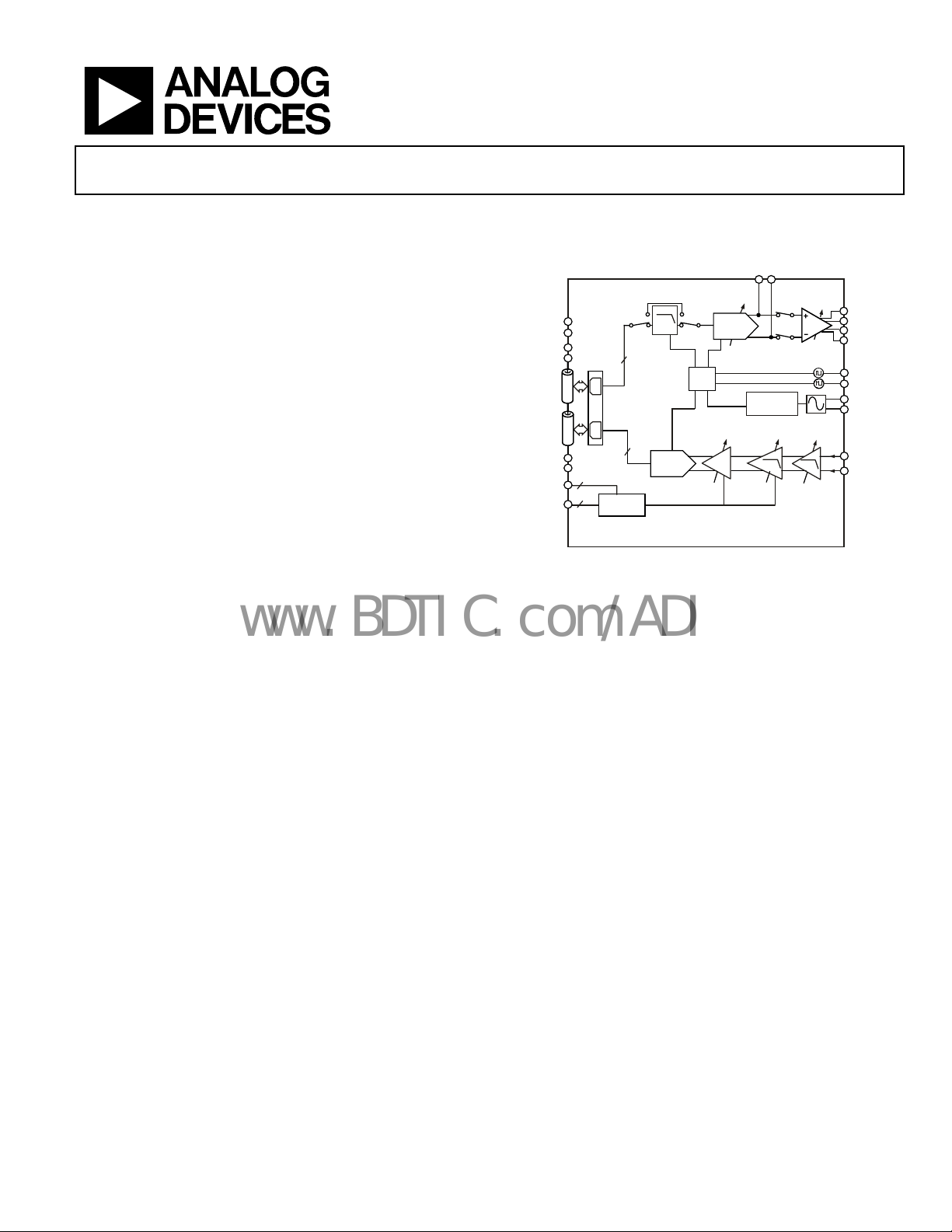
FUNCTIONAL BLOCK DIAGRAM
AD9865
6
4
SPI
REGISTER
CONTROL
2-4X
10
10
ADC
80MSPS
CLK
SYN.
0 TO 6dB
∆ = 1dB
TxDAC
0 TO –7.5dB
– 6 TO 18dB
∆ = 6dB
Figure 1.
IOUT_P+
IOUT_P–
2M CLK
MULTIPLIER
2-POLE
LPF
–6 TO 24dB
∆ = 6dB
AD9865
IOUT_G+
IAMP
0 TO –12dB
1-POLE
LPF
IOUT_N+
IOUT_N–
IOUT_G–
CLKOUT_1
CLKOUT_2
OSCIN
XTAL
RX+
RX–
04493-0-001
GENERAL DESCRIPTION
The AD9865 is a mixed-signal front end (MxFE) IC for
transceiver applications requiring Tx and Rx path functionality
with data rates up to 80 MSPS. Its flexible digital interface,
power saving modes, and high Tx-to-Rx isolation make it well
suited for half- and full-duplex applications. The digital interface is extremely flexible allowing simple interfaces to digital
back ends that support half- or full-duplex data transfers, thus
often allowing the AD9865 to replace discrete ADC and DAC
solutions. Power saving modes include the ability to reduce
power consumption of individual functional blocks, or to power
down unused blocks in half-duplex applications. A serial port
interface (SPI®) allows software programming of the various
functional blocks. An on-chip PLL clock multiplier and
synthesizer provide all the required internal clocks, as well as
two external clocks from a single crystal or clock source.
The Tx signal path consists of a bypassable 2×/4× low-pass
interpolation filter, a 10-bit TxDAC, and a line driver. The
transmit path signal bandwidth can be as high as 34 MHz at an
input data rate of 80 MSPS. The TxDAC provides differential
current outputs that can be steered directly to an external load
or to an internal low distortion current amplifier. The current
amplifier (IAMP) can be configured as a current- or voltagemode line driver (with two external npn transistors) capable of
delivering in excess of 23 dBm peak signal power. Tx power can
be digitally controlled over a 19.5 dB range in 0.5 dB steps.
The receive path consists of a programmable amplifier
(RxPGA), a tunable low-pass filter (LPF), and a 10-bit ADC.
The low noise RxPGA has a programmable gain range of
−12 dB to +48 dB in 1 dB steps. Its input referred noise is less
than 3 nV/rtHz for gain settings beyond 36 dB. The receive path
LPF cutoff frequency can be set over a 15 MHz to 35 MHz
range or simply bypassed. The 10-bit ADC achieves excellent
dynamic performance over a 5 MSPS to 80 MSPS span. Both
the RxPGA and the ADC offer scalable power consumption
allowing power/performance optimization.
The AD9865 provides a highly integrated solution for many
broadband modems. It is available in a space saving 64-pin chip
scale package and is specified over the commercial (−40°C to
+85°C) temperature range.
Rev. A
Information furnished by Analog Devices is believed to be accurate and reliable.
However, no responsibility is assumed by Analog Devices for its use, nor for any
infringements of patents or other rights of third parties that may result from its use.
Specifications subject to change without notice. No license is granted by implication
or otherwise under any patent or patent rights of Analog Devices. Trademarks and
registered trademarks are the property of their respective owners.
One Technology Way, P.O. Box 9106, Norwood, MA 02062-9106, U.S.A.
Tel: 781.329.4700 www.analog.com
Fax: 781.326.8703 © 2004 Analog Devices, Inc. All rights reserved.
Page 2

AD9865
www.BDTIC.com/ADI
TABLE OF CONTENTS
Specifications..................................................................................... 3
TxDAC and IAMP Architecture .............................................. 28
Tx Path Specifications.................................................................. 3
Rx Path Specifications.................................................................. 4
Power Supply Specifications ....................................................... 5
Digital Specifications ................................................................... 6
Serial Port Timing Specifications............................................... 7
Half-Duplex Data Interface (ADIO Port) Timing
Specifications ................................................................................ 7
Full-Duplex Data Interface (Tx and Rx Port) Timing
Specifications ................................................................................ 8
Explanation of Test Levels........................................................... 8
Absolute Maximum Ratings............................................................ 9
Thermal Characteristics .............................................................. 9
ESD Caution.................................................................................. 9
Pin Configuration and Function Descriptions........................... 10
Typical Performance Characteristics ........................................... 12
Rx Path Typical Performance Characteristics ........................ 12
TxDAC Path Typical Performance Characteristics ...............16
IAMP Path Typical Performance Characteristics.................. 18
Serial Port ........................................................................................19
Register Map Description .........................................................21
Serial Port Interface (SPI) ......................................................... 21
Digital Interface ..............................................................................23
Half-Duplex Mode..................................................................... 23
Full-Duplex Mode ...................................................................... 24
RxPGA Control .......................................................................... 25
TxPGA Control ..........................................................................27
Transm i t P a t h .................................................................................. 28
Tx Programmable Gain Control.............................................. 30
TxDAC Output Operation........................................................ 30
IAMP Current-Mode Operation.............................................. 30
IAMP Voltage-Mode Operation .............................................. 31
IAMP Current Consumption Considerations........................ 32
Receive Path .................................................................................... 33
Rx Programmable Gain Amplifier........................................... 33
Low-Pass Filter ........................................................................... 34
Analog-to-Digital Converter (ADC)....................................... 35
AGC Timing Considerations.................................................... 36
Clock Synthesizer........................................................................... 37
Power Control and Dissipation .................................................... 39
Power-Down ............................................................................... 39
Half-Duplex Power Savings ...................................................... 39
Power Reduction Options ......................................................... 40
Power Dissipation ...................................................................... 42
Mode Select upon Power-Up and Reset.................................. 42
Analog and Digital Loop-Back Test Modes............................ 43
PCB Design Considerations.......................................................... 44
Component Placement.............................................................. 44
Power Planes and Decoupling .................................................. 44
Ground Planes ............................................................................ 44
Signal Routing ............................................................................ 44
Evaluation Board ............................................................................ 46
Outline Dimensions ....................................................................... 47
Ordering Guide .......................................................................... 47
Digital Interpolation Filters ......................................................28
REVISION HISTORY
11/04—Data Sheet Changed from Rev. 0 to Rev. A
Changes to Specifications Tables.................................................... 3
Changes to Serial Table.................................................................. 19
Changes to Full Duplex Mode section......................................... 24
Change to TxDAC and IAMP Architecture section.................. 29
Rev. A | Page 2 of 48
Change to TxDAC Output Operation section............................ 30
Insert equation................................................................................ 37
Change to Figure 84 caption ......................................................... 42
11/03—Revision 0: Initial Version
Page 3
AD9865
www.BDTIC.com/ADI
SPECIFICATIONS
Tx PATH SPECIFICATIONS
AVDD = 3.3 V ± 5%, DVDD = CLKVDD = DRVDD = 3.3 V ± 10%; f
noted.
Table 1.
Parameter Temp Test Level Min Typ Max Unit
TxDAC DC CHARACTERISTICS
Resolution Full 10 Bits
Update Rate Full II 200 MSPS
Full-Scale Output Current (IOUTP_FS) Full IV 2 25 mA
Gain Error
Offset Error 25°C V 2 µA
Voltage Compliance Range Full −1 +1.5 V
TxDAC GAIN CONTROL CHARACTERISTICS
Minimum Gain 25°C V −7.5 dB
Maximum Gain 25°C V 0 dB
Gain Step Size 25°C V 0.5 dB
Gain Step Accuracy 25°C IV Monotonic
Gain Range Error 25°C V ±2 dB
TxDAC AC CHARACTERISTICS
Fundamental 0.5 dBm
Signal-to-Noise and Distortion (SINAD) Full IV 62.0 63.1 dBc
Signal-to-Noise Ratio (SNR) Full IV 62.5 63.2 dBc
Total Harmonic Distortion (THD) Full IV −77.7 −67.0 dBc
Spurious-Free Dynamic Range (SFDR) Full IV 67.1 79.3 dBc
IAMP DC CHARACTERISTICS
IOUTN Full-Scale Current = IOUTN+ + IOUTN− Full IV 2 105 mA
IOUTG Full-Scale Current = IOUTG+ + IOUTG− Full IV 2 150 mA
AC Voltage Compliance Range Full IV 1 7 V
IAMPN AC CHARACTERISTICS
Fundamental 25°C 13 dBm
IOUTN SFDR (Third Harmonic) Full IV 43.3 45.2 dBc
IAMP GAIN CONTROL CHARACTERISTICS
Minimum Gain 25°C V −19.5 dB
Maximum Gain 25°C V 0 dB
Gain Step Size 25°C V 0.5 dB
Gain Step Accuracy 25°C IV Monotonic dB
IOUTN Gain Range Error 25°C V 0.5 dB
REFERENCE
Internal Reference Voltage
Reference Error Full V 0.7 3.4 %
Reference Drift Full V 30 ppm/oC
Tx DIGITAL FILTER CHARACTERISTICS (2× Interpolation)
Latency (Relative to 1/f
−0.2 dB Bandwidth Full V 0.2187 f
−3 dB Bandwidth Full V 0.2405 f
Stop-Band Rejection (0.289 f
1
2
3
4
) Full V 43 Cycles
DAC
to 0.711 f
DAC
) Full V 50 dB
DAC
= 50 MHz, f
OSCIN
25°C I ±2 % FS
25°C I 1.23 V
= 200 MHz, R
DAC
= 2.0 kΩ, unless otherwise
SET
OUT/fDAC
OUT /fDAC
Rev. A | Page 3 of 48
Page 4
AD9865
www.BDTIC.com/ADI
Parameter Temp Test Level Min Typ Max Unit
Tx DIGITAL FILTER CHARACTERISTICS (4× Interpolation)
Latency (Relative to 1/ F
−0.2 dB Bandwidth Full V 0.1095 f
−3 dB Bandwidth Full V 0.1202 f
Stop Band Rejection (0.289 f
PLL CLK MULTIPLIER
OSCIN Frequency Range Full IV 5 80 MHz
Internal VCO Frequency Range Full IV 20 200 MHz
Duty Cycle Full II 40 60 %
OSCIN Impedance 25°C V 100//3 ΜΩ/pF
CLKOUT1 Jitter
CLKOUT2 Jitter
5
6
CLKOUT1 and CLKOUT2 Duty Cycle
1
Gain error and gain temperature coefficients are based on the ADC only (with a fixed 1.23 V external reference and a 1 V p-p differential analog input).
2
TxDAC IOUTFS = 20 mA, differential output with 1:1 transformer with source and load termination of 50 Ω, F
3
IOUN full-scale current = 80 mA, f
4
Use external amplifier to drive additional load.
5
Internal VCO operates at 200 MHz , set to divide-by-1.
6
Because CLKOUT2 is a divided down version of OSCIN, its jitter is typically equal to OSCIN.
7
CLKOUT2 is an inverted replica of OSCIN, if set to divide-by-1.
) Full V 96 Cycles
DAC
OUT/fDAC
OUT /fDAC
OSCIN
to 0.711 f
) Full V 50 dB
OSCIN
25°C III 12 ps rms
25°C III 6 ps rms
= 80 MHz, f
OSCIN
7
=160 MHz, 2x interpolation.
DAC
Full III 45 55 %
= 5 MHz, 4x interpolation.
OUT
Rx PATH SPECIFICATIONS
AVDD = 3.3 V ± 5%, DVDD = CLKVDD = DRVDD = 3.3 V ± 10%; half- or full-duplex operation with CONFIG = 0 default power bias
settings, unless otherwise noted.
Table 2.
Parameter Temp Test Level Min Typ Max Unit
Rx INPUT CHARACTERISTICS
Input Voltage Span (RxPGA Gain = −10 dB) Full III 6.33 V p-p
Input Voltage Span (RxPGA Gain = +48 dB) Full III 8 mV p-p
Input Common-Mode Voltage 25°C III 1.3
Differential Input Impedance 25°C III
400
4.0
Input Bandwidth (with RxLPF Disabled, RxPGA = 0 dB) 25°C III 53 MHz
Input Voltage Noise Density (RxPGA Gain = 36 dB, f
Input Voltage Noise Density (RxPGA Gain = 48 dB, f
= 26 MHz) 25°C III 3.0 nV/rtHz
−3 dBF
−3 dBF
= 26 MHz)
25°C III 2.4 nV/rtHz
RxPGA CHARACTERISTICS
Minimum Gain 25°C III −12 dB
Maximum Gain 25°C III 48 dB
Gain Step Size 25°C III 1 dB
Gain Step Accuracy 25°C III Monotonic dB
Gain Range Error 25°C III 0.5 dB
RxLPF CHARACTERISTICS
Cutoff Frequency (f
Attenuation at 55.2 MHz with f
) Range Full III 15 35 MHz
−3 dBF
= 21 MHz 25°C III 20 dB
−3 dBF
Pass-Band Ripple 25°C III ±1 dB
Settling Time to 5 dB RxPGA Gain Step @ f
Settling Time to 60 dB RxPGA Gain Step @ f
= 50 MSPS 25°C III 20 ns
ADC
= 50 MSPS 25°C III 100 ns
ADC
ADC DC CHARACTERISTICS
Resolution NA NA 10 Bits
Conversion Rate Full II 5 80 MSPS
V
Ω
pF
Rev. A | Page 4 of 48
Page 5
AD9865
www.BDTIC.com/ADI
Parameter Temp Test Level Min Typ Max Unit
Rx PATH LATENCY1
Full-Duplex Interface Full V 10.5 Cycles
Half-Duplex Interface Full V 10.0 Cycles
Rx PATH COMPOSITE AC PERFORMANCE @ f
= 50 MSPS
ADC
RxPGA Gain = 48 dB (Full-Scale = 8.0 mV p-p)
Signal-to-Noise and Distortion (SNR) 25°C III 43.7 dBc
Total Harmonic Distortion (THD) 25°C III −71 dBc
RxPGA Gain = 24 dB (Full-Scale =126 mV p-p)
Signal-to-Noise (SNR) 25°C III 59 dBc
Total Harmonic Distortion (THD) 25°C III −67.2 dBc
RxPGA Gain = 0 dB (Full-Scale = 2.0 V p-p)
Signal-to-Noise and Distortion (SINAD) Full IV 58 59 dBc
Total Harmonic Distortion (THD) Full IV −66 −62.9 dBc
Rx PATH COMPOSITE AC PERFORMANCE @ f
= 80 MSPS3
ADC
RxPGA Gain = 48 dB (Full-Scale = 8.0 mV p-p)
Signal-to-Noise (SNR) 25°C III 41.8 dBc
Total Harmonic Distortion (THD) 25°C III −67 dBc
RxPGA Gain = 24 dB (Full-Scale = 126 mV p-p)
Signal-to-Noise (SNR) 25°C III 58.6 dBc
Total Harmonic Distortion (THD) 25°C III −62.9 dBc
RxPGA Gain = 0 dB (Full-Scale = 2.0 V p-p)
Signal-to-Noise (SNR) 25°C II 58.9 59.6 dBc
Total Harmonic Distortion (THD) 25°C II −69.7 −59.8 dBc
Rx-to-Tx PATH FULL-DUPLEX ISOLATION
(1 V p-p, 10 MHz Sine Wave Tx Output)
RxPGA Gain = 40 dB
IOUTP± Pins to RX± Pins 25°C III 83 dBc
IOUTG± Pins to RX± Pins 25°C III 37 dBc
RxPGA Gain = 0 dB
IOUTP± Pins to RX± Pins 25°C III 123 dBc
IOUTG± Pins to RX± Pins 25°C III 77 dBc
1
Includes RxPGA, ADC pipeline, and ADIO bus delay relative to f
2
fIN = 5 MHz, AIN = −1.0 dBFS , LPF cutoff frequency set to 15.5 MHz with Reg. 0x08 = 0x80.
3
fIN = 5 MHz, AIN = −1.0 dBFS , LPF cutoff frequency set to 26 MHz with Reg. 0x08 = 0x80.
POWER SUPPLY SPECIFICATIONS
AVDD = 3.3 V, DVDD = CLKVDD = DRVDD = 3.3 V; R
Table 3.
Parameter Temp Test Level Min Typ Max Unit
SUPPLY VOLTAGES
AVDD Full V 3.135 3.3 3.465 V
CLKVDD Full V 3.0 3.3 3.6 V
DVDD Full V 3.0 3.3 3.6 V
DRVDD Full V 3.0 3.3 3.6 V
IS_TOTAL (Total Supply Current) Full II 406 475 mA
POWER CONSUMPTION
I
+ I
AVDD
I
+ I
DVDD
(Analog Supply Current)
CLKVDD
(Digital Supply Current) Full IV 95 133 mA
DRVDD
2
.
ADC
= 2 kΩ, full-duplex operation with f
SET
= 80 MSPS,1 unless otherwise noted.
DATA
IV 311 342 mA
Rev. A | Page 5 of 48
Page 6
AD9865
www.BDTIC.com/ADI
Parameter Temp Test Level Min Typ Max Unit
POWER CONSUMPTION (Half-Duplex Operation with f
Tx Mode
I
+ I
AVDD
CLKVDD
I
+ I
DVDD
DRVDD
Rx Mode
I
+ I
AVDD
CLKVDD
I
+ I
DVDD
DRVDD
POWER CONSUMPTION OF FUNCTIONAL BLOCKS1 (I
RxPGA and LPF 25°C III 87 mA
ADC 25°C III 108 mA
TxDAC 25°C III 38 mA
IAMP (Programmable) 25°C III 10 120 mA
Reference 25°C III 170 mA
CLK PLL and Synthesizer 25°C III 107 mA
MAXIMUM ALLOWABLE POWER DISSIPATION Full IV 1.66 W
STANDBY POWER CONSUMPTION
IS_TOTAL (Total Supply Current) Full
POWER DOWN DELAY (USING PWR_DWN PIN)
RxPGA and LPF 25°C III 440 ns
ADC 25°C III 12 ns
TxDAC 25°C III 20 ns
IAMP 25°C III 20 ns
CLK PLL and synthesizer 25°C III 27 ns
POWER UP DELAY (USING PWR_DWN PIN)
RxPGA and LPF 25°C III 7.8 µs
ADC 25°C III 88 ns
TxDAC 25°C III 13 µs
IAMP 25°C III 20 ns
CLK PLL and Synthesizer 25°C III 20 µs
1
Default power-up settings for MODE = HIGH and CONFIG = LOW, IOUTP_FS = 20 mA, does not include IAMP’s current consumption, which is application dependent.
2
Default power-up settings for MODE = LOW and CONFIG = LOW.
DIGITAL SPECIFICATIONS
AVDD = 3.3 V ± 5%, DVDD = CLKVDD = DRVDD = 3.3 V ± 10%; R
Table 4.
Parameter Temp Test Level Min Typ Max Unit
CMOS LOGIC INPUTS
High Level Input Voltage Full VI DRVDD – 0.7 V
Low Level Input Voltage Full VI 0.4 V
Input Leakage Current 12 µA
Input Capacitance Full VI 3 pF
CMOS LOGIC OUTPUTS (C
High Level Output Voltage (IOH = 1 mA) Full VI DRVDD – 0.7 V
Low Level Output Voltage (IOH = 1 mA) Full VI 0.4 V
Output Rise/Fall Time (High Strength Mode and C
Output Rise/Fall Time (Low Strength Mode and C
Output Rise/Fall Time (High Strength Mode and C
Output Rise/Fall Time (Low Strength Mode and C
RESET
Minimum Low Pulse Width (Relative to f
= 5 pF)
LOAD
) 1
ADC
= 50 MSPS)2
DATA
25°C IV 112 130 mA
25°C IV 46 49.5 mA
25°C IV 225 253 mA
25°C IV 36.5 39 mA
+ I
AVDD
= 15 pF) Full VI 1.5/2.3 ns
LOAD
= 15 pF) Full VI 1.9/2.7 ns
LOAD
= 5 pF) Full VI 0.7/0.7 ns
LOAD
= 5 pF) Full VI 1.0/1.0 ns
LOAD
)
CLKVDD
= 2 kΩ, unless otherwise noted.
SET
13 mA
Clock
cles
cy
Rev. A | Page 6 of 48
Page 7

AD9865
www.BDTIC.com/ADI
SERIAL PORT TIMING SPECIFICATIONS
AVDD = 3.3 V ± 5%, DVDD = CLKVDD = DRVDD = 3.3 V ± 10%, unless otherwise noted.
Table 5.
Parameter Temp Test Level Min Typ Max Unit
WRITE OPERATION (See Figure 46)
SCLK Clock Rate (f
SCLK Clock High (tHI) Full IV 14 ns
SCLK Clock Low (t
SDIO to SCLK Setup Time (tDS) Full IV 14 ns
SCLK to SDIO Hold Time (tDH) Full IV 0 ns
SEN to SCLK Setup Time (tS)
SCLK to SEN Hold Time (tH)
READ OPERATION (See Figure 47 and Figure 48)
SCLK Clock Rate (f
SCLK Clock High (tHI) Full IV 14 ns
SCLK Clock Low (t
SDIO to SCLK Setup Time (tDS) Full IV 14 ns
SCLK to SDIO Hold Time (tDH) Full IV 0 ns
SCLK to SDIO (or SDO) Data Valid Time (tDV) Full IV 14 ns
SEN to SDIO Output Valid to Hi-Z (tEZ)
) Full IV 32 MHz
SCLK
) Full IV 14 ns
LOW
Full IV 14 ns
Full IV 0 ns
) Full IV 32 MHz
SCLK
) Full IV 14 ns
LOW
Full IV 2 ns
HALF-DUPLEX DATA INTERFACE (ADIO PORT) TIMING SPECIFICATIONS
AVDD = 3.3 V ± 5%, DVDD = CLKVDD = DRVDD = 3.3 V ± 10%, unless otherwise noted.
Table 6.
Parameter Temp Test Level Min Typ Max Unit
READ OPERATION1 (See Figure 50)
Output Data Rate Full II 5 80 MSPS
Three-State Output Enable Time (t
Three-State Output Disable Time (t
Rx Data Valid Time (tVT) Full II 1.5 ns
Rx Data Output Delay (tOD) Full II 4 ns
WRITE OPERATION (See Figure 49)
Input Data Rate (1× Interpolation) Full II 20 80 MSPS
Input Data Rate (2× Interpolation) Full II 10 80 MSPS
Input Data Rate (4× Interpolation) Full II 5 50 MSPS
Tx Data Setup Time (tDS) Full II 1 ns
Tx Data Hold Time (tDH) Full II 2.5 ns
Latch Enable Time (tEN) Full II 3 ns
Latch Disable Time (t
) Full II 3 ns
DIS
) Full II 3 ns
PZL
) Full II 3
PLZ
1
C
= 5 pF for digital data outputs.
LOAD
ns
Rev. A | Page 7 of 48
Page 8

AD9865
www.BDTIC.com/ADI
FULL-DUPLEX DATA INTERFACE (Tx AND Rx PORT) TIMING SPECIFICATIONS
AVDD = 3.3 V ± 5%, DVDD = CLKVDD = DRVDD = 3.3 V ± 10%, unless otherwise noted.
Table 7.
Parameter Temp Test Level Min Typ Max Unit
Tx PATH INTERFACE (See Figure 53)
Input Nibble Rate (2× Interpolation) Full II 20 160 MSPS
Input Nibble Rate (4× Interpolation) Full II 10 100 MSPS
Tx Data Setup Time (tDS) Full II 2.5 ns
Tx Data Hold Time (tDH) Full II 1.5 ns
Rx PATH INTERFACE1 (See Figure 54)
Output Nibble Rate Full II 10 160 MSPS
Rx Data Valid Time (tDV) Full II 3 ns
Rx Data Hold Time (tDH) Full II 0 ns
1
C
=5 pF for digital data outputs.
LOAD
EXPLANATION OF TEST LEVELS
I 100% production tested.
II 100% production tested at 25°C and guaranteed by desig
III Sample tested only.
IV Parameter is guaranteed by design and charac
V Parameter is a typical value only.
VI 100% production tested at 25°C and guaranteed by design and char
terization testing.
n and characterization at specified temperatures.
acterization for industrial temperature range.
Rev. A | Page 8 of 48
Page 9

AD9865
www.BDTIC.com/ADI
ABSOLUTE MAXIMUM RATINGS
Table 8.
Parameter Rating
ELECTRICAL
AVDD, CLKVDD Voltage 3.9 V maximum
DVDD, DRVDD Voltage 3.9 V maximum
RX+, RX−, REFT, REFB −0.3 V to AVDD + 0.3 V
IOUTP+, IOUTP− −1.5 V to AVDD + 0.3 V
IOUTN+, IOUTN−, IOUTG+,
IOUTG−
OSCIN, XTAL −0.3 V to CLVDD + 0.3 V
REFIO, REFADJ −0.3 V to AVDD + 0.3 V
Digital Input and Output Voltage −0.3 V to DRVDD + 0.3 V
Digital Output Current 5 mA maximum
ENVIRONMENTAL
Operating Temperature Range
(Ambient)
Maximum Junction Temperature 125°C
Lead Temperature (Soldering, 10 s) 150°C
Storage Temperature Range
(Ambient)
−0.3 V to +7 V
−40°C to +85°C
−65°C to +150°C
Stresses above those listed under the Absolute Maximum
Ratings may cause permanent damage to the device. This is a
stress rating only; functional operation of the device at these or
any other conditions above those indicated in the operational
section of this specification is not implied. Exposure to absolute
maximum rating conditions for extended periods may affect
device reliability.
THERMAL CHARACTERISTICS
Thermal Resistance: 64-lead LFCSP (4-layer board).
= 24°C/W (paddle soldered to ground plane, 0 LPM air).
θ
JA
= 30.8°C/W (paddle not soldered to ground plane,
θ
JA
0 LPM air).
ESD CAUTION
ESD (electrostatic discharge) sensitive device. Electrostatic charges as high as 4000 V readily accumulate on
the human body and test equipment and can discharge without detection. Although this product features
proprietary ESD protection circuitry, permanent damage may occur on devices subjected to high energy
electrostatic discharges. Therefore, proper ESD precautions are recommended to avoid performance
degradation or loss of functionality.
Rev. A | Page 9 of 48
Page 10
AD9865
T
www.BDTIC.com/ADI
PIN CONFIGURATION AND FUNCTION DESCRIPTIONS
DRVDD
DRVSS
PWR_DWN
CLKOUT2
DVDD
DVSS
CLKVDD
OSCIN
XTAL
CLKVSS
CONFIG
ADIO9/Tx[5]
ADIO8/Tx[4]
ADIO7/Tx[3]
ADIO6/Tx[2]
ADIO5/Tx[1]
ADIO4/Tx[0]
ADIO3/Rx[5]
ADIO2/Rx[4]
ADIO1/Rx[3]
ADIO0/Rx[2]
NC/Rx[1]
NC/Rx[0]
RXEN/RXSYNC
TXEN/TXSYNC
XCLK/TXQUIET
RXCLK
64
63 62 61 60 595857 56 55 54 535251 50
1
2
3
4
5
6
7
8
9
10
11
12
13
14
15
16
PIN 1
IDENTIFIER
AD9865
TOP VIEW
(Not to Scale)
MODE
IOUT_P–
IOUT_P+
IOUT_G+
IOUT_N+
49
3217 18 19 20 21 22 23 24 25 26 27 282930 31
48
47
46
45
44
43
42
41
40
39
38
37
36
35
34
33
AVSS
AVSS
IOUT_N–
IOUT_G–
AVSS
AVDD
REFIO
REFADJ
AVDD
AVSS
RX+
RX–
AVSS
AVDD
AVSS
REFT
DRVDD
DRVSS
CLKOUT1
SCLK
PGA[4]
PGA[3]
PGA[2]
PGA[1]
PGA[0]
GAIN/PGA[5]
RESET
AVSS
REFB
SEN
SDO
SDIO
Figure 2. Pin Configuration
Table 9. Pin Function Descriptions
Pin No. Mnemonic Mode
1
Description
1 ADIO9 HD MSB of ADIO Buffer
Tx[5] FD MSB of Tx Nibble Input
2 to 5 ADIO8 to 5 HD Bits 8 to 5 of ADIO Buffer
Tx[4 to 1] FD Bits 4 to 1 of Tx Nibble Input
6 ADIO4 HD Bit 4 of ADIO Buffer
Tx[0] FD LSB of Tx Nibble Input
7 ADIO3 HD Bit 3 of ADIO Buffer
Rx[5] FD MSB of Rx Nibble Output
8, 9 ADIO2, 1 HD Bits 2 to 1 of ADIO Buffer
Rx[4, 3] FD Bits 4 to 3 of Rx Nibble Output
10 ADIO0 HD LSB of ADIO Buffer
Rx[2] FD Bit 2 of Rx Nibble Output
11 NC HD No Connect
Rx[1] FD Bit 1 of Rx Nibble Output
12 NC HD No Connect
Rx[0] FD LSB of Rx Nibble Output
13 RXEN HD ADIO Buffer Control Input
RXSYNC FD Rx Data Synchronization Output
14 TXEN HD Tx Path Enable Input
TXSYNC FD Tx Data Synchronization Input
4493-0-002
Rev. A | Page 10 of 48
Page 11
AD9865
www.BDTIC.com/ADI
Pin No. Mnemonic Mode
15 TXCLK HD ADIO Sample Clock Input
16 RXCLK HD ADIO Request Clock Input
FD Rx and Tx Clock Output at 2 x f
17, 64 DRVDD Digital Output Driver Supply Input
18, 63 DRVSS Digital Output Driver Supply Return
19 CLKOUT1
20 SDIO Serial Port Data Input/Output
21 SDO Serial Port Data Output
22 SCLK Serial Port Clock Input
23
24 GAIN FD Tx Data Port (Tx[5:0]) Mode Select
PGA[5] HD or FD MSB of PGA Input Data Port
25 to 29 PGA[4 to 0] HD or FD Bits 4 to 0 of PGA Input Data Port
30
31, 34, 36, 39, 44, 47, 48 AVSS Analog Ground
32, 33 REFB, REFT ADC Reference Decoupling Nodes
35, 40, 43 AVDD Analog Power Supply Input
37, 38 RX−, RX+ Receive Path − and + Analog Inputs
41 REFADJ TxDAC Full-Scale Current Adjust
42 REFIO TxDAC Reference Input/Output
45 IOUT_G− −Tx Amp Current Output_Sink
46 IOUT_N− −Tx Mirror Current Output_Sink
49 IOUT_G+ +Tx Amp Current Output_Sink
50 IOUT_N+ +Tx Mirror Current Output_Sink
51 IOUT_P− −TxDAC Current Output_Source
52 IOUT_P+ +TxDAC Current Output_Source
53 MODE
54 CONFIG Power-Up SPI Register Default Setting Input
55 CLKVSS Clock Oscillator/Synthesizer Supply Return
56 XTAL Crystal Oscillator Inverter Output
57 OSCIN Crystal Oscillator Inverter Input
58 CLKVDD Clock Oscillator/Synthesizer Supply
59 DVSS Digital Supply Return
60 DVDD Digital Supply Input
61 CLKOUT2
62 PWR_DWN Power-Down Input
TXQUIET
SEN
RESET
1
Description
FD Fast TxDAC/IAMP Power-Down
Serial Port Enable Input
Reset Input (Active Low)
f
/N Clock Output (L = 1, 2, 4, or 8)
ADC
Digital Interface Mode Select Input
OW = HD, HIGH = FD
L
f
/L Clock Output, (L = 1, 2, or 4)
OSCIN
ADC
1
HD = half-duplex mode; FD = full-duplex mode.
Rev. A | Page 11 of 48
Page 12
AD9865
www.BDTIC.com/ADI
TYPICAL PERFORMANCE CHARACTERISTICS
Rx PATH TYPICAL PERFORMANCE CHARACTERISTICS
AVDD = CLKVDD = DVDD = DRVDD = 3.3 V, f
RIN = 50 Ω, half- or full-duplex interface, default power bias settings.
10
0
–10
–20
–30
–40
–50
–60
–70
–80
INPUT REFERRED SPECTRUM (dBm)
–90
–100
0 6.25 12.50 18.75 25.00
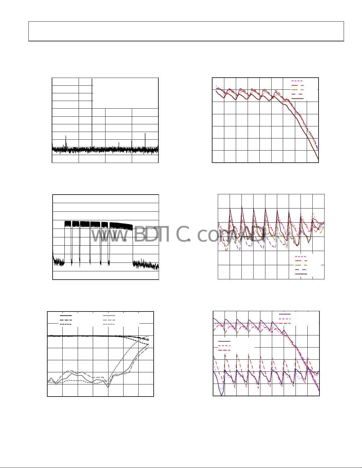
Figure 3. Spectral Plot with 4 k FFT of Input Sinusoid with
RxPGA = 0 dB and P
–30
–40
–50
–60
–70
–80
–90
–100
–110
INPUT REFERRED SPECTRUM (dBm)
–120
–130
0 5 10 15 20 25
Figure 4. Spectral Plot with 4 k FFT of 84-Carrier DMT Signal
with PAR = 10.2 dB, P
66
63
FUND = –1dBFS
SINAD = 59.1dBFS
ENOB = 9.53 BITS
SNR = 60.2dBFS
THD = –65.2dBFS
SFDR = –64.9dBc (THIRD HARMONIC)
RBW = 12.21kHz
FREQUENCY (MHz)
= 9 dBm
IN
RBW = 12.2kHz
FREQUENCY (MHz)
= −33.7 dBm, and RxPGA = 36 dB
IN
OSCIN
= f
= 50 MSPS, low-pass filter’s f
ADC
04493-0-040
04493-0-041
–50
–56
= 22 MHz, AIN = −1 dBFS,
−3 dB
62
59
56
53
50
SINAD (dBFS)
47
44
41
–6 0 6 12 18 24 30 36 42 48
RxPGA GAIN (dB)
Figure 6. SINAD/ENOB vs. RxPGA Gain and Frequency
–55
–60
–65
–70
THD (dBFC)
–75
–80
–85
–6 0 6 12 18 24 30 36 42 48
RxPGA GAIN (dB)
Figure 7. THD vs. RxPGA Gain and Frequency
62
59
SINAD @ +25°C
SINAD @ +85°C
SINAD @ –40°C
1MHz
5MHz
10MHz
15MHz
20MHz
1MHz
5MHz
10MHz
15MHz
20MHz
10.0
9.5
9.0
8.5
8.0
7.5
7.0
6.5
–45
–50
ENOB (Bits)
04493-0-043
04493-0-044
60
57
54
SINAD (dBFS)
51
48
45
–21 –18 –15 –12 –9 –6 –3 0
SINAD @ 3.14V
SINAD @ 3.3V
SINAD @ 3.46V
INPUT AMPLITUDE (dBFS)
0dBFS = 2V p-p
THD @ 3.14V
THD @ 3.3V
THD @ 3.46V
–62
–68
–74
–80
–86
–92
THD (dBFS)
04493-0-042
Figure 5. SINAD and THD vs. Input Amplitude and Supply
= 8 MHz, LPF f
(f
IN
= 26 MHz; Rx PGA = 0 dB)
−3 dB
Rev. A | Page 12 of 48
56
53
50
SINAD (dBFS)
47
44
41
–6 0 6 12 18 24 30 36 42 48
THD @ +25°C
THD @ +85°C
THD @ –40°C
RxPGA GAIN (dB)
Figure 8. SINAD/THD Performance vs. RxPGA Gain
and Temperature ( f
= 5 MHz)
IN
–55
–60
–65
–70
–75
–80
THD (dBc)
04493-0-045
Page 13
AD9865
–
–
www.BDTIC.com/ADI
Rx PATH TYPICAL PERFORMANCE CHARACTERISTICS
AVDD = CLKVDD = DVDD = DRVDD = 3.3 V, f
RIN = 50 Ω, half- or full-duplex interface, default power bias settings.
10
0
–10
–20
–30
–40
–50
–60
–70
–80
INPUT REFERRED SPECTRUM (dBm)
–90
–100
0 1020304
Figure 9. Spectral Plot with 4k FFT of Input Sinusoid
with RxPGA = 0 dB and P
–30
–40
–50
–60
–70
–80
–90
–100
–110
INPUT REFERRED SPECTRUM (dBm)
–120
–130
0 1020304
Figure 10. Spectral Plot with 4k FFT of 111-Carrier DMT Signal with
PAR = 11 dB, P
66
63
= −33.7 dBm, LPF f
IN
SINAD @ 3.14V
SINAD @ 3.3V
SINAD @ 3.46V
FUND = –1dBFS
SINAD = 59.3dBFS
ENOB = 9.56 BITS
SNR = 59.8dBFS
THD = –69.1dBFS
SFDR = –70.3dBc (THIRD HARMONIC)
RBW = 19.53kHz
FREQUENCY (MHz)
= 9 dBm
IN
RBW = 19.53kHz
FREQUENCY (MHz)
= 32 MHz, and RxPGA = 36 dB
−3 dB
THD @ 3.14V
THD @ 3.3V
THD @ 3.46V
OSCIN
= f
= 80 MSPS, low-pass filter’s f
ADC
04493-0-046
0
04493-0-047
0
–50
–56
= 30 MHz, AIN = −1 dBFS,
−3 dB
62
59
56
53
50
SINAD (dBFS)
47
44
41
–6 0 6 12 18 24 30 36 42 48
RxPGA GAIN (dB)
Figure 12. SINAD/ENOB vs. RxPGA Gain and Frequency
55
–60
–65
–70
THD (dBc)
–75
–80
–85
–6 0 6 12 18 24 30 36 42 48
RxPGA GAIN (dB)
Figure 13. THD vs. RxPGA Gain and Frequency
62
59
SINAD @ +25°C
SINAD @ +85°C
SINAD @ –40°C
5MHz
10MHz
15MHz
20MHz
30MHz
5MHz
10MHz
15MHz
20MHz
30MHz
10.0
9.5
9.0
8.5
8.0
7.5
7.0
6.5
–45
ENOB (Bits)
04493-0-049
04493-0-050
40
60
57
54
SINAD (dBFS)
51
48
45
–21 –18 –15 –12 –9 –6 –3 0
INPUT AMPLITUDE (dBFS)
0dBFS = 2V p-p
–62
–68
–74
–80
–86
–92
THD (dBFS)
04493-0-048
Figure 11. SINAD and THD vs. Input Amplitude and Supply
= 8 MHz, LPF f
(f
IN
= 26 MHz; RxPGA = 0 dB)
−3 dB
Rev. A | Page 13 of 48
56
53
50
SINAD (dBFS)
47
44
41
–6 0 6 12 18 24 30 36 42 48
THD @ +25°C
THD @ +85°C
THD @ –40°C
RxPGA GAIN (dB)
–50
–55
–60
–65
–70
–75
Figure 14. SINAD/THD Performance vs. RxPGA Gain and Temperature
= 10 MHz)
( f
IN
THD (dBc)
04493-0-051
Page 14
AD9865
–
www.BDTIC.com/ADI
61.0
60.5
60.0
59.5
59.0
58.5
58.0
SNR (dBFS)
57.5
57.0
56.5
56.0
–6 0 6 12 18 24 30 36 42 48
THD @ 3.13V
THD @ 3.3V
THD @ 3.47V
INPUT FREQUENCY (MHz)
SNR @ 3.13V
SNR @ 3.3V
SNR @ 3.47V
Figure 15. SNR and THD vs. Input Frequency and Supply
= 26 MHz; RxPGA = 0 dB)
( LPF f
−3 dB
109.4
98.5
87.5
76.6
65.6
54.7
43.8
32.8
INTEGRATED NOISE (µV rms)
21.9
10.9
0
–6 0 6 12 18 24 30 36 42 48
RxPGA GAIN (dB)
AD9865: +25°C
AD9865: +85°C
AD9865: –40°C
Figure 16. Input Referred Integrated Noise and Noise Spectral Density vs.
RxPGA Gain (LPF f
5
4
3
2
1
0
–1
–2
DC OFFSET (% of full-scale)
–3
–4
–5
–6 0 6 12 18 24 30 36 42 48
−3 dB
GAIN (dB)
= 26 MHz)
DEVICE 1
DEVICE 2
DEVICE 3
DEVICE 4
Figure 17. Rx DC Offset vs. RxPGA Gain
52
–54
–56
–58
–60
–62
–64
–66
–68
–70
–72
20
18
16
14
12
10
8
6
4
2
0
THD (dBc)
04493-0-052
NOISE SPECTRAL DENSITY (nV/ Hz)
04493-0-053
04493-0-054
60.0
59.5
59.0
58.5
58.0
57.5
57.0
SNR (dBFS)
56.5
56.0
55.5
55.0
20 30 40 50 60 70 80
SNR @ 3.13V
SNR @ 3.3V
SNR @ 3.46V
THD @ 3.13V
THD @ 3.3V
THD @ 3.46V
INPUT FREQUENCY (MHz)
Figure 18. SNR and THD vs. Sample Rate and Supply
(LPF Disabled; RxPGA = 0 dB; f
45
44
43
42
41
SNR (dBc)
40
39
38
0 1020304050607080
CUTOFF FREQUENCY (MHz)
= 8 MHz)
IN
Figure 19. SNR vs. Filter Cutoff Frequency
(50 MSPS; f
0.5
0.4
0.3
0.2
0.1
0
–0.1
–0.2
GAIN STEP ERROR (dB)
–0.3
–0.4
–0.5
–6 0 6 12 18 24 30 36 42 48
Figure 20. RxPGA Gain Step Error vs. Gain (f
= 5 MHz; AIN = −1 dB; RxPGA = 48 dB)
IN
AD9865: GAIN STEP ERROR @ +25°C
AD9865: GAIN STEP ERROR @ +85°C
AD9865: GAIN STEP ERROR @ –40°C
RxPGA GAIN (dB)
= 10 MHz)
IN
–20
–30
–40
–50
–60
–70
THD (dBc)
04493-0-055
04493-0-056
04493-0-057
Rev. A | Page 14 of 48
Page 15
AD9865
www.BDTIC.com/ADI
Rx PATH TYPICAL PERFORMANCE CHARACTERISTICS
AVDD = CLKVDD = DVDD = DRVDD = 3.3 V, f
RIN = 50 Ω, half- or full-duplex interface, default power bias settings.
512
448
384
320
CODE
256
192
128
64
0 80 160 240 320 400 480 560 640 720
Figure 21. RxPGA Settling Time −12 dB to +48 dB Transition for DC Input
(f
ADC
0
–3
–6
–9
–12
AMPLITUDE RESPONSE (dB)
–15
–18
0 5 10 15 20 25 30 35 40 45 50
Figure 22. Rx Low-Pass Filter Amplitude Response vs. Supply
(f
= 50 MSPS, f
ADC
140
130
120
(dB)
110
100
@RxPGA = 0dB
90
ATTEN
80
70
60
0 5 10 15 20 25 30 35
Figure 23. Rx to Tx Full-Duplex Isolation @ 0 RxPGA Setting
(Note: ATTEN
@ RxPGA = x dB
TIME (ns)
= 50 MSPS, LPF Disabled)
INPUT FREQUENCY (MHz)
= 33 MHz, RxPGA = 0 dB)
−3 dB
TxDAC ISOLATION @ 0dB
IAMP ISOLATION @ 0dB
FREQUENCY (MHz)
= ATTEN
@ RxPGA = 0 dB
− RxPGA Gain)
OSCIN
3.3V
3.0V
3.6V
= f
= 50 MSPS, low-pass filter disabled, RxPGA = 0 dB, AIN = −1 dBFS,
ADC
352
320
288
256
224
CODE
192
160
128
96
04493-0-058
64
0 80 160 240 320 400 480 560 640 720
TIME (ns)
Figure 24. RxPGA Settling Time for 0 dB to +5 dB Transition for DC Input
= 50 MSPS, LPF Disabled)
(f
ADC
0
–2
–4
–6
–8
04493-0-059
–10
–12
FUNDAMENTAL (dB)
–14
–16
–18
–20
0 5 10 15 20 25 30 35 40 5045
+18dB GAIN
+30dB GAIN
+42dB GAIN
INPUT FREQUENCY (MHz)
Figure 25. Rx Low-Pass Filter Amplitude Response vs. RxPGA Gain
04493-0-060
(LPF's f
420
410
400
390
)
Ω
380
370
360
RESISTANCE (
350
340
330
320
5 105958575655545352515
= 33 MHz)
3 dB
−
R
IN
C
IN
FREQUENCY (MHz)
Figure 26. Rx Input Impedance vs. Frequency
–6dB GAIN
0dB GAIN
+6dB GAIN
10
9
8
7
6
5
4
3
2
1
0
04493-0-061
04493-0-062
CAPACITANCE (pF)
04493-0-090
Rev. A | Page 15 of 48
Page 16

AD9865
www.BDTIC.com/ADI
TxDAC PATH TYPICAL PERFORMANCE CHARACTERISTICS
AVDD = CLKVDD = DVDD = DRVDD = 3.3 V, f
(see Figure 63) into 50 Ω load half- or full-duplex interface, default power bias settings.
10
0
–10
–20
–30
dBm
–40
–50
–60
–70
–80
0 5 10 15 20 30
Figure 27. Dual-Tone Spectral Plot of TxDAC's Output
= 50 MSPS, 4× Interpolation, 10 dBm Peak Power,
(f
DATA
–65
FREQUENCY (MHz)
F1 = 17 MHz, F2 = 18 MHz)
= 50 MSPS and 80 MSPS, RSET = 1.96 kΩ, 2:1 transformer coupled output
OSCIN
10
0
–10
–20
–30
dBm
–40
–50
–60
–70
04493-0-072
–80
0 5 10 15 20 25 30 35 40
Figure 30. Dual-Tone Spectral Plot of TxDAC's Output
(f
DATA
–65
FREQUENCY (MHz)
= 80 MSPS, 2× Interpolation, 10 dBm Peak Power,
F1 = 27.1 MHz, F2 = 28.7 MHz)
04493-0-075
–70
–75
–80
IMD (dBFS)
(RELATIVE TO PEAK POWER)
–85
–90
0 2.5 5.0 7.5 10.0 12.5 15.0 17.5 20.0
2-TONE CENTER FREQUENCY (MHz)
4dBm
7dBm
Figure 28. 2-Tone IMD Frequency Sweep vs. Peak Power
= 50 MSPS, 4× Interpolation
with f
DATA
–65
–70
–75
–80
SFDR (dBFS)
(RELATIVE TO PEAK POWER)
–85
10dBm
4dBm
7dBm
10dBm
04493-0-073
–70
10dBm
–75
–80
IMD (dBFS)
(RELATIVE TO PEAK POWER)
–85
–90
0 5 10 15 20 25 30
4dBm
7dBm
2-TONE CENTER FREQUENCY (MHz)
Figure 31. 2-Tone IMD Frequency Sweep vs. Peak Power
= 80 MSPS, 2× Interpolation
with f
DATA
–65
–70
10dBm
–75
–80
SFDR (dBFS)
(RELATIVE TO PEAK POWER)
–85
4dBm
7dBm
04493-0-076
–90
0 2.5 5.0 7.5 10.0 12.5 15.0 17.5 20.0
2-TONE CENTER FREQUENCY (MHz)
04493-0-074
Figure 29. 2-Tone Worst Spur Frequency Sweep vs. Peak Power
= 50 MSPS, 4× Interpolation
with f
DATA
Rev. A | Page 16 of 48
–90
0 5 10 15 20 25 30
2-TONE CENTER FREQUENCY (MHz)
Figure 32. 2-Tone Worst Spur Frequency Sweep vs. Peak Power
= 80 MSPS, 2× Interpolation
with f
DATA
04493-0-077
Page 17

AD9865
www.BDTIC.com/ADI
–20
–30
PAR = 11.4
RMS = –1.4dBm
–20
–30
PAR = 11.4
RMS = –1.4dBm
–40
–50
–60
dBm
–70
–80
–90
–100
0 5 10 15 20 25
FREQUENCY (MHz)
Figure 33. Spectral Plot of 84-Carrier OFDM Test Vector
= 50 MSPS, 4× Interpolation)
(f
DATA
–20
–30
–40
–50
–60
dBm
–70
–80
–90
–100
0 25 50 75 100 125 150 175 200
FREQUENCY (MHz)
PAR = 11.4
RMS = –1.4dBm
Figure 34. Wideband Spectral Plot of 88-Subcarrier OFDM Test Vector
= 50 MSPS, 4× Interpolation)
(f
DATA
100
95
90
85
80
75
70
(RELATIVE TO PEAK POWER)
65
SNR AND 2-TONE IMD (dBFS)
60
55
–24 –21 –18 –15 –12 –9 –6 –3 0
Figure 35. SNR and SFDR vs. P
(f
= 12.55 MHz, f
OUT
DATA
2-TONE IMD
SNR
AOUT (dBFS)
OUT
= 50 MSPS, 4× Interpolation)
04493-0-078
04493-0-079
04493-0-080
–40
–50
–60
dBm
–70
–80
–90
–100
0 5 10 15 20 25 30 35 40
FREQUENCY (MHz)
Figure 36. Spectral Plot of 111-Carrier OFDM Test Vector
= 80 MSPS, 2× Interpolation)
(f
DATA
–20
–30
–40
–50
–60
dBm
–70
–80
–90
–100
0 20 40 60 80 100 120 140 160
FREQUENCY (MHz)
PAR = 11.4
RMS = –1.4dBm
Figure 37. Wideband Spectral Plot of 111-Carrier OFDM Test Vector
= 80 MSPS, 2× Interpolation)
(f
DATA
95
90
85
80
75
70
(RELATIVE TO PEAK POWER)
65
SNR AND 2-TONE IMD (dBFS)
60
55
–24 –21 –18 –15 –12 –9 –6 –3 0
Figure 38. SNR and SFDR vs. P
(f
= 20 MHz, f
OUT
2-TONE IMD
SNR
AOUT (dBFS)
= 80 MSPS, 2× Interpolation)
DATA
OUT
04493-0-081
04493-0-082
04493-0-083
Rev. A | Page 17 of 48
Page 18

AD9865
www.BDTIC.com/ADI
IAMP PATH TYPICAL PERFORMANCE CHARACTERISTICS
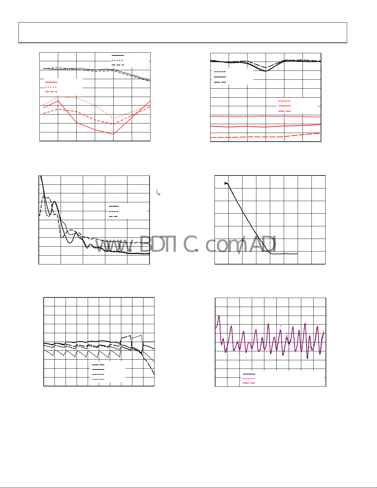
AVDD = CLKVDD = DVDD = DRVDD = 3.3 V, f
Figure 65) into 50 Ω load, half- or full-duplex interface, default power bias settings.
20
15
10
5
0
–5
–10
–15
–20
dBm
–25
–30
–35
–40
–45
–50
–55
–60
0 5 10 15 20 25
Figure 39. Dual-Tone Spectral Plot of IAMPN Output
(IAMP Settings of I = 12.5 mA, N = 4, G = 0,
2:1 Transformer into 75 Ω Loader, VCM = 4.8 V)
0
–10
–20
–30
–40
dBm
–50
–60
–70
–80
0 5 10 15 20 25
Figure 40. Spectral Plot of 84-Carrier OFDM Test Vector Using IAMPN in
(IAMP Settings of I = 10 mA, N = 4, G = 0; VCM = 4.8 V)
0
–10
–20
FREQUENCY (MHz)
FREQUENCY (MHz)
Current-Mode Configuration
PAR = 11.4
RMS = 10.3dBm
PAR = 11.4
RMS = 10.4dBm
= 50 MSPS, R
OSCIN
RBW = 2.3kHz
= 1.58 kΩ, 1:1 transformer coupled output (see Figure 64 and
SET
04493-0-084
Figure 42. IOUTN Third-Order Intercept vs. Common-Mode Voltage
04493-0-085
Figure 43. IOUTG Third-Order Intercept vs. Common-Mode Voltage
48
46
44
42
40
38
OIP3 (dBm)
36
34
32
30
3.0 3.5 4.0 4.5 5.0
15MHz
VCM (V)
2.5MHz
20MHz
(IAMP Settings of I = 12.5 mA, N = 4, G = 0, 2:1
Transformer into 75 Ω Load)
42
40
38
36
OIP3 (dBm)
34
32
30
3.0 3.5 4.0 4.5 5.0
VCM (V)
2.5MHz
5MHz
10MHz
15MHz
20MHz
(IAMP Settings of I = 4.25 mA, N = 0, G = 6,
2:1 Transformer into 75 Ω Load)
0
–10
–20
PAR = 11.4
RMS = 9.8dBm
RBW = 10kHz
5MHz
10MHz
04493-0-087
04493-0-088
–30
–40
dBm
–50
–60
–70
–80
0 5 10 15 20 25
FREQUENCY (MHz)
04493-0-086
Figure 41. Spectral Plot of 84-Carrier OFDM Test Vector Using IAMP in
Voltage-Mode Configuration with AVDD = 5 V
(PBR951 Transistors, IAMP Settings of I = 6 mA, N = 2, G = 6)
Rev. A | Page 18 of 48
–30
–40
dBm
–50
–60
–70
–80
0 5 10 15 20 25
FREQUENCY (MHz)
04493-0-089
Figure 44. Spectral Plot of 84-Carrier OFDM Test Vector Using IAMP in
Voltage-Mode Configuration with AVDD = 3.3 V
(PBR951 Transistors, IAMP Settings of I = 6 mA, N = 2, G = 6)
Page 19

AD9865
www.BDTIC.com/ADI
SERIAL PORT
Table 10. SPI Register Mapping
Bit
Address
(Hex)
SPI PORT CONFIGURATION AND SOFTWARE RESET
0x00 (7) 4-Wire SPI 1 0 0 0 0
(6) LSB First 1 0 0 0 0
(5) S/W Reset 1 0 0 0 0
POWER CONTROL REGISTERS (via PWR_DWN pin)
0x01 (7)
(6) TxDAC/IAMP 1 0 0 0 0
(5) Tx Digital 1 0 0 0 0
(4) REF 1 0 0 0 0
(3) ADC CML 1 0 0 0 0
(2) ADC 1 0 0 0 0
(1) PGA Bias 1 0 0 0 0
(0) RxPGA 1 0 0 0 0
0x02 (7)
(6) TxDAC/IAMP 1 1 1 1 1
(5) Tx Digital 1 1 1 1 1
(4) REF 1 1 1 1 1
(3) ADC CML 1 1 1 1 1
(2) ADC 1 1 1 1 1
(1) PGA Bias 1 1 1 1 1
(0) RxPGA 1 1 1 1 1
HALF-DUPLEX POWER CONTROL
0x03 (7:3) Tx OFF Delay 5
(2) Rx _TXEN 1
(1) Tx PWRDN 1
(0) Rx PWRDN 1
PLL CLOCK MULTIPLIER/SYNTHESIZER CONTROL
0x04 (5) Duty Cycle Enable 1 0 0 0 0
(3:2) PLL Divide-N 2 00 00 00 00
(1:0) PLL Multiplier-M 2 01 10* 01 01
0x05 (2) OSCIN to RXCLK 1 0 0 0 1*
(1) Invert RXCLK 1 0 0 0 0
(0) Disabled RXCLK 1 0 0 0 0
0x06 (7:6) CLKOUT2 Divide 2 01 01 01 01
(5) CLKOUT2 Invert 1 0 0 0 0
(4) CLKOUT2 Disable 1 0 0 0 1*
(3:2) CLKOUT1 Divide 2 01 01 01 01
(1) CLKOUT1 Invert 1 0 0 0 0
(0) CLKOUT1 Disable 1 0 0 0 1*
Rx PATH CONTROL
0x07 (5) Initiate Offset Cal. 1 0 0 0 0
(4) Rx Low Power 1 0 1* 0 1*
(0) Rx Filter ON 1 1 1 1 1
Break-
1
down Description
(4) f
Width
Clock Syn.
CLK Syn.
from PLL 1 0 0 0 0
ADC
1 0 0 0 0
1 0 0 0 1*
MODE = 0 (Half-Duplex) MODE = 1 (Full-Duplex)
CONFIG = 0 CONFIG = 1 CONFIG = 0 CONFIG = 1
0xFF
0xFF N/A N/A
Power-Up Default Value
Comments
Default SPI configuration is
3-
wire, MSB first.
PWR_DWN = 0.
Default setting is for all
bloc
ks powered on.
PWR_DWN = 1.
Default setting* is for all
functional blocks powered
down except PLL.
*MODE = CONFIG = 1.
Setting has PLL powered
wn with OSCIN input
do
routed to RXCLK output.
Default setting is for TXEN
input to c
on/off of Tx/Rx path.
Tx driver delayed by 31
clock cycles.
1/f
DATA
Default setting is Duty Cycle
R
estore disabled, ADC CLK
from OSCIN input, and PLL
multiplier × 2 setting.
*PLL multiplier × 4 setting.
Full-duplex RXCLK normally
a
t nibble rate.
*Exception on power-up.
Default setting is CLKOUT2
and CLK
divide-by-2.
*CLKOUT1 and CLKOUT2
dis
Default setting has LPF ON
and Rx pa
power bias setting.
*Rx path to low power.
OUT1 enabled with
abled.
ontrol power
th at nominal
Rev. A | Page 19 of 48
Page 20

AD9865
www.BDTIC.com/ADI
Bit
Address
(Hex)
0x08 (7:0)
Tx/Rx PATH GAIN CONTROL
0x09 (6) Use SPI Rx Gain 1
(5:0) Rx Gain Code 6
0x0A (6) Use SPI Tx Gain 1
(5:0) Tx Gain Code 6
Tx AND Rx PGA CONTROL
0x0B (6) PGA Code for Tx 1 0 0 0 0
(5) PGA Code for Rx 1 1 1 1 1
(3) Force GAIN strobe 1 0 0 0 0
(2) Rx Gain on Tx Port 1 0 0 1* 1*
(1) 3-Bit RxPGA Port 1 0 1** 0 0
Tx DIGITAL FILTER AND INTERFACE
0x0C (7:6)
(4)
(3) Tx 5/5 Nibble* 1 N/A N/A 0 0
(2) LS Nibble First* 1 N/A N/A 0 0
(1) TXCLK neg. edge 1 0 0 0 0
(0) Twos complement 1 0 0 1 1
Rx INTERFACE AND ANALOG/DIGITAL LOOPBACK
0x0D (7) Analog Loopback 1 0 0 0 0
(6) Digital Loopback* 1 0 0 0 0
(5) Rx Port 3-State 1 N/A N/A 0 0
(4)
(3) RX 5/5 Nibble 1 N/A N/A 0 0
(2) LS Nibble First* 1 N/A N/A 0 0
(1) RXCLK neg. edge 1 0 0 0 0
(0) Twos complement 1 0 0 1 1
DIGITAL OUTPUT DRIVE STRENGTH, TxDAC OUTPUT, AND REV ID
0x0E (7)
(0) TxDAC Output 1 0 0 0 0
0x0F (3:0) REV ID Number 4 0x00 0x00 0x00 0x00
Tx IAMP GAIN AND BIAS CONTROL
0x10 (7) Select Tx Gain 1
(6:4) G1 3
(2:0) N 3
0x11 (6:4) G2 3
(2:0) G3 3
0x12 (6:4) Stand_Secondary 3
(2:0) Stand_Primary 3
Break-
1
down Description
Width
Rx Filter Tuning
Cut-off Frequency
Interpolation
Fac tor
Invert
EN/TXSYNC
TX
Invert
EN/RXSYNC
RX
Low Drive
ength
Str
8
2 01 00 01 01
1 0 0 0 0
1 0 0 0 0
1 0 0 0 0
MODE = 0 (Half-Duplex) MODE = 1 (Full-Duplex)
CONFIG = 0 CONFIG = 1 CONFIG = 0 CONFIG = 1
0x80 0x61 0x80 0x80
0x00
0x00 0x00 0x00
0x7F 0x7F 0x7F 0x7F
0x44 0x44 0x44
0x44
0x62 0x62 0x62
0x62
0x01
0x01 0x01 0x01
Power-Up Default Value
Comments
Refer to Low-Pass Filter
section.
Default setting is for
hardware Rx gain code via
PGA or Tx data port.
Default setting is for Tx gain
code via SPI control.
Default setting is RxPGA
ontrol active.
c
*Tx port with GAIN strobe
AD9875/AD9876-compatible).
(
** 3-bit RxPGA gain map
AD9975-compatible).
(
Default setting is 2×
interpolation with LPF
response. Data format is
straight binary for halfduplex and twos
complement for full-duplex
interface.
*Full-duplex only.
Data format is straight
binar
y for half-duplex and
twos complement for fullduplex interface.
Analog loopback: ADC Rx
da
ta fed back to TxDAC.
Digital loopback: Tx input
da
ta to Rx output port.
*Full-duplex only.
Default setting is for high
e strength and IAMP
driv
enabled.
Secondary path G1 = 0, 1, 2,
3, 4.
Primary path N = 0, 1, 2, 3, 4.
Secondary path stages:
G2 = 0 to 1.50 in 0.25 steps
and G3 = 0 to 6.
Standing current of primary
and sec
ondary path.
Rev. A | Page 20 of 48
Page 21

AD9865
www.BDTIC.com/ADI
Bit
Address
(Hex)
0x13
1
Bits that are undefined should always be assigned a 0.
Break-
1
down Description
(7:5) CPGA Bias Adjust 3
(4:3) SPGA Bias Adjust 2
(2:0) ADC Bias Adjust 4
Width
MODE = 0 (Half-Duplex) MODE = 1 (Full-Duplex)
CONFIG = 0 CONFIG = 1 CONFIG = 0 CONFIG = 1
0x00 0x00 0x00 0x00
REGISTER MAP DESCRIPTION
The AD9865 contains a set of programmable registers described
in Table 10 that are used to optimize its numerous features,
interface options, and performance parameters from its default
register settings. Registers pertaining to similar functions have
been grouped together and assigned adjacent addresses to
minimize the update time when using the multibyte serial port
interface (SPI) read/write feature. Bits that are undefined within
a register should be assigned a 0 when writing to that register.
The default reg
applications to operate without the use of an SPI. The AD9865
can be configured to support a half- or full-duplex digital
interface via the MODE pin, with each interface having two
possible default register settings determined by the setting of
the CONFIG pin.
For instance, applications that need to use only the Tx or Rx
pa
th functionality of the AD9865 can configure it for a halfduplex interface (MODE = 0), and use the TXEN pin to select
between the Tx or Rx signal path with the unused path
remaining in a reduced power state. The CONFIG pin can be
used to select the default interpolation ratio of the Tx path and
RxPGA gain mapping.
ister settings were intended to allow some
SERIAL PORT INTERFACE (SPI)
The serial port of the AD9865 has 3- or 4-wire SPI capability
allowing read/write access to all registers that configure the
device’s internal parameters. Registers pertaining to the SPI are
listed in Table 11. The default 3-wire serial communication port
consists of a clock (SCLK), serial port enable (
directional data (SDIO) signal.
gating read and write cycle. When
are three-stated. The inputs to SCLK,
Schmitt trigger with a nominal hysteresis of 0.4 V centered
about VDDH/2. The SDO pin remains three-stated in a 3-wire
SPI interface.
is an active low control
SEN
SEN
SEN
SEN
), and a bi-
is high, SDO and SDIO
, and SDIO contain a
Power-Up Default Value
Comments
Current bias setting for Rx
pa
th’s functional blocks.
Refer to page 41.
Table 11. SPI Registers Pertaining to SPI Options
Address (Hex) Bit Description
0x00 (7) Enable 4-wire SPI
A 4-wire SPI can be enabled by setting the 4-wire SPI bit high,
causing the output data to appear on the SDO pin instead of on
the SDIO pin. The SDIO pin serves as an input-only throughout
the read operation. Note that the SDO pin is active only during
the transmission of data and remains three-stated at any other
time.
An 8-bit instruction header must accompany each read and
wr
ite operation. The instruction header is shown in Table 12.
The MSB is an R/
read operation. The next two bits, N1 and N0, specify the
number of bytes (one to four bytes) to be transferred during the
data transfer cycle. The remaining five bits specify the address
bits to be accessed during the data transfer portion. The data
bits immediately follow the instruction header for both read
and write operations.
Table 12. Instruction Header Information
MSB LSB
17 16 15 14 13 12 11 10
R/W
The AD9865 serial port can support both MSB (most
significant bit) first and LSB (least significant bit) first data
formats. Figure 45 illustrates how the serial port words are built
for the MSB first and LSB first modes. The bit order is controlled by the SPI LSB first bit (Register 0, Bit 6). The default
value is 0, MSB first. Multibyte data transfers in MSB format
can be completed by writing an instruction byte that includes
the register address of the last address to be accessed. The
AD9865 automatically decrements the address for each successive byte required for the multibyte communication cycle.
W
N1 N0 A4 A3 A2 A1 A0
(6) Enable SPI LSB first
indicator bit with logic high indicating a
Rev. A | Page 21 of 48
Page 22

AD9865
S
S
S
www.BDTIC.com/ADI
SEN
SCLK
DATA
SEN
SCLK
DATA
INSTRUCTION CYCLE
R/W
N1
A1
A0 N2
A3A4A0N2
A2A3A4
A2
Figure 45. SPI Timing, MSB First (Upper), and LSB First (Lower)
When the SPI LSB first bit is set high, the serial port interprets
both instruction and data bytes LSB first. Multibyte data transfers in LSB format can be completed by writing an instruction
byte that includes the register address of the first address to be
accessed. The AD9865 automatically increments the address for
each successive byte required for the multibyte communication
cycle.
Figure 46 illustrates the timing requirements for a write operation to the SPI port. After the serial port enable (
goes low, data (SDIO) pertaining to the instruction header is
read on the rising edges of the clock (SCLK). To initiate a write
operation, the read/not-write bit is set low. After the instruction
header is read, the eight data bits pertaining to the specified
register are shifted into the SDIO pin on the rising edge of the
next eight clock cycles. If a multibyte communication cycle is
specified, the destination address is decremented (MSB first)
and shifts in another eight bits of data. This process repeats until
all the bytes specified in the instruction header (N1, N0 bits) are
shifted into the SDIO pin.
SEN
transfer operation, only going high after the last bit is shifted
into the SDIO pin.
DATA TRANSFER CYCLE
D1
SEN
D0
N
N
D7ND6
N
) signal
A1
D71D6
1
DATA TRANSFER CYCLEINSTRUCTION CYCLE
N1
R/W
D01D1
1
must remain low during the data
4493-0-003
Figure 47 illustrates the timing for a 3-wire read operation to
the SPI port. After
goes low, data (SDIO) pertaining to the
SEN
instruction header is read on the rising edges of SCLK. A read
operation occurs, if the read/not-write indicator is set high.
After the address bits of the instruction header are read, the
eight data bits pertaining to the specified register are shifted out
of the SDIO pin on the falling edges of the next eight clock cycles.
If a multibyte communication cycle is specified in the instruction
header, a similar process as previously described for a multibyte
SPI write operation applies. The SDO pin remains three-stated
in a 3-wire read operation.
t
f
1/
S
SEN
CLK
SDIO
SCLK
t
t
t
DS
LOW
HI
t
DV
A0
D6
D7
t
EZ
D0
D1
R/W
t
DH
A1
N1
A2
Figure 47. SPI 3-Wire Read Operation Timing
Figure 48 illustrates the timing for a 4-wire read operation to
the SPI port. The timing is similar to the 3-wire read operation
with the exception that data appears at the SDO pin, while the
SDIO pin remains high impedance throughout the operation.
The SDO pin is an active output only during the data transfer
phase and remains three-stated at all other times.
t
f
1/
S
SEN
SCLK
SDIO
SDO
SCLK
t
t
t
DS
LOW
HI
t
R/W
DH
A1
N1
A2
A0
t
DV
D7D6D1
Figure 48. SPI 4-Wire Read Operation Timing
t
EZ
t
EZ
D0
4493-0-005
4493-0-006
SEN
SCLK
SDIO
SCLK
t
t
LOW
HI
t
DS
t
R/W
DH
N1 N0
A0
D7
t
H
D1
D6
D0
4493-0-004
t
f
1/
S
Figure 46. SPI Write Operation Timing
Rev. A | Page 22 of 48
Page 23

AD9865
A
www.BDTIC.com/ADI
DIGITAL INTERFACE
The digital interface port is configurable for half-duplex or fullduplex operation by pin-strapping the MODE pin low or high,
respectively. In half-duplex mode, the digital interface port
becomes a 10-bit bidirectional bus called the ADIO port. In
full-duplex mode, the digital interface port is divided into two
6-bit ports called Tx[5:0] and Rx[5:0] for simultaneous Tx and
Rx operations. In this mode, data is transferred between the
ASIC and AD9865 in 6-bit (or 5-bit) nibbles. The AD9865 also
features a flexible digital interface for updating the RxPGA and
TxPGA gain registers via a 6-bit PGA port or Tx[5:0] port for
fast updates, or via the SPI port for slower updates. See the
RxPGA Control section for more information.
HALF-DUPLEX MODE
The half-duplex mode functions as follows when the MODE
pin is tied low. The bidirectional ADIO port is typically shared
in burst fashion between the transmit path and receive path.
Two control signals, TXEN and RXEN, from a DSP (or digital
ASIC) control the bus direction by enabling the ADIO port’s
input latch and output driver, respectively. Two clock signals are
also used: TXCLK to latch the Tx input data, and RXCLK to
clock the Rx output data. The ADIO port can also be disabled
by setting TXEN and RXEN low (default setting), thus allowing
it to be connected to a shared bus.
Internally, the ADIO port consists of an input latch for the Tx
path in parallel with an output latch with three-state outputs for
the Rx path. TXEN is used to enable the input latch; RXEN is
used to three-state the output latch. A five-sample-deep FIFO is
used on the Tx and Rx paths to absorb any phase difference between the AD9865’s internal clocks and the externally supplied
clocks (TXCLK, RXCLK). The ADIO bus accepts input datawords into the transmit path when the TXEN pin is high, the
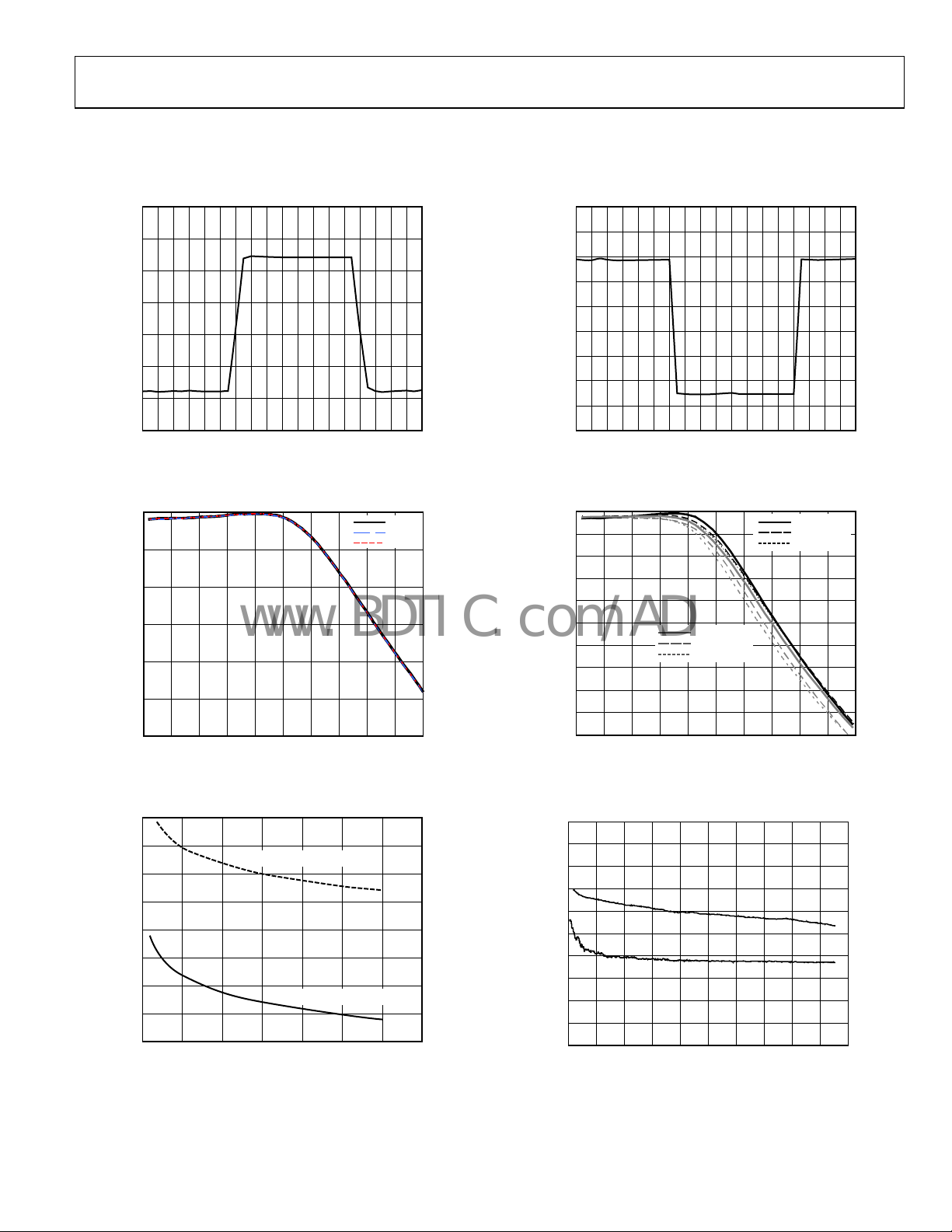
RXEN pin is low, and a clock is present on the TXCLK pin, as
shown in Figure 49.
t
DS
TXCLK
TXEN
ADIO[9:0]
RXEN
t
EN
TX0
Figure 49. Transmit Data Input Timing Diagram
t
DH
TX2
TX3 TX4TX1
The Tx interpolation filter(s) following the ADIO port can be
flushed with zeros, if the clock signal into the TXCLK pin is
present for 33 clock cycles after TXEN goes low. Note that the
data on the ADIO bus is irrelevant over this interval.
The output from the receive path is driven onto the ADIO bus
when the RXEN pin is high, and a clock is present on the RXCLK
pin. While the output latch is enabled by RXEN, valid data
t
DIS
4493-0-007
appears on the bus after a 6-clock-cycle delay due to the internal
FIFO delay. Note that Rx data is not latched back into the Tx
path, if TXEN is high during this interval with TXCLK present.
The ADIO bus becomes three-stated once the RXEN pin returns
low. Figure 50 shows the receive path output timing.
RXCLK
RXEN
DIO[9:0]
t
PZL
Figure 50. Receive Data Output Timing Diagram
t
VT
RX0 RX1 RX2 RX3
t
OD
t
PLZ
To add flexibility to the digital interface port, several programming options are available in the SPI registers. These options
are listed in Table 13. The default Tx and Rx data input formats
are straight binary, but can be changed to twos complement.
The default TXEN and RXEN settings are active high, but can
be set to opposite polarities, thus allowing them to share the
same control. In this case, the ADIO port can still be placed
onto a shared bus by disabling its input latch via the control
signal, and disabling the output driver via the SPI register. The
clock timing can be independently changed on the transmit and
receive paths by selecting either the rising or falling clock edge
as the validating/sampling edge of the clock. Lastly, the output
driver’s strength can be reduced for lower data rate applications.
Table 13. SPI Registers for Half-Duplex Interface
Address (Hex) Bit Description
0x0C (4) Invert TXEN
(1) TXCLK negative edge
(0) Twos complement
0x0D (5) Rx port three-state
(4) Invert RXEN
(1) RXCLK negative edge
(0) Twos complement
0x0E (7) Low digital drive strength
The half-duplex interface can be configured to act as a slave or a
master to the digital ASIC. An example of a slave configuration
is shown in Figure 51. In this example, the AD9865 accepts all
the clock and control signals from the digital ASIC. Because the
sampling clocks for the DAC and ADC are derived internally
from the OSCIN signal, the TXCLK and RXCLK signals must
be at exactly the same frequency as the OSCIN signal. The
phase relationships among the TXCLK, RXCLK, and OSCIN
signals can be arbitrary. If the digital ASIC cannot provide a low
jitter clock source to OSCIN, use the AD9865 to generate the
clock for its DAC and ADC, and to pass the desired clock signal
to the digital ASIC via CLKOUT1 or CLKOUT2.
4493-0-008
Rev. A | Page 23 of 48
Page 24

AD9865
www.BDTIC.com/ADI
ADIO
[9:0]
RXEN
TXEN
TXCLK
RXCLK
OSCIN
AD9865
10
10
TO
Tx DIGITAL
FILTER
FROM
Rx ADC
4493-0-009
DIGITAL ASIC
Tx/Rx
Data[9:0]
DAC_CLK
ADC_CLK
CLKOUT
RXEN
TXEN
Figure 51. Example of a Half-Duplex Digital Interface
with AD9865 Serving as the Slave
Figure 52 shows a half-duplex interface with the AD9865 acting
as the master, generating all the required clocks. CLKOUT1
provides a clock equal to the bus data rate that is fed to the
ASIC as well as back to the TXCLK and RXCLK inputs. This
interface has the advantage of reducing the digital ASIC’s pin
count by three. The ASIC needs only to generate a bus control
signal that controls the data flow on the bidirectional bus.
ADIO
[9:0]
RXEN
TXEN
TXCLK
RXCLK
CLKOUT1
OSCIN
AD9865
10
TO
Tx DIGITAL
FILTER
10
FROM
Rx ADC
4493-0-010
DIGITAL ASIC
Tx/Rx
Data[9:0]
BUS_CTR
CLKIN
Figure 52. Example of a Half-Duplex Digital Interface
FROM
CRYSTAL
OR MASTER CLK
with AD9865 Serving as the Master
FULL-DUPLEX MODE
The full-duplex mode interface is selected when the MODE pin
is tied high. It can be used for full- or half-duplex applications.
The digital interface port is divided into two 6-bit ports called
Tx[5:0] and Rx[5:0], allowing simultaneous Tx and Rx operations for full-duplex applications. In half-duplex applications,
the Tx[5:0] port can also be used to provide a fast update of the
RxPGA (AD9875 backward-compatible) during an Rx operation. This feature is enabled by default and can be used to
reduce the required pin count of the ASIC (refer to RxPGA
Control section for details).
In either application, Tx and Rx data are transferred between
the ASIC and AD9865 in 6-bit (or 5-bit) nibbles at twice the
internal input/output word rates of the Tx interpolation filter
and ADC. Note that the TxDAC update rate must not be less
than the nibble rate. Therefore, the 2× or 4× interpolation filter
must be used with a full-duplex interface.
The AD9865 acts as the master, providing RXCLK as an output
clock that is used for the timing of both the Tx[5:0] and Rx[5:0]
ports. RXCLK always runs at the nibble rate and can be inverted
or disabled via an SPI register. Because RXCLK is derived from
the clock synthesizer, it remains active, provided that this functional block remains powered on. A buffered version of the
signal appearing at OSCIN can also be directed to RXCLK by
setting Bit 2 of Register 0x05. This feature allows the AD9865 to
be completely powered down (including the clock synthesizer)
while serving as the master.
The Tx[5:0] port operates in the following manner with the SPI
register default settings. Two consecutive nibbles of the Tx data
are multiplexed together to form a 10-bit data-word in twos
complement format. The clock appearing on the RXCLK pin is
a buffered version of the internal clock used by the Tx[5:0]
port’s input latch with a frequency that is always twice the ADC
sample rate (2 × f
). Data from the Tx[5:0] port is read on the
ADC
rising edge of this sampling clock, as illustrated in the timing
diagram shown in Figure 53. Note,
TXQUIET
must remain
high for the reconstructed Tx data to appear as an analog signal
at the output of the TxDAC or IAMP.
t
DS
t
SU
RXCLK
t
HD
t
TXSYNC
Tx[5:0]
Tx0LSB
Tx1MSB Tx1LSB
DH
Tx2MSB
Tx3LSB
Tx2LSB
Tx3MSB
4493-0-011
Figure 53. Tx[5:0] Port Full-Duplex Timing Diagram
The TXSYNC signal is used to indicate to which word a nibble
belongs. While TXSYNC is low, the first nibble of every word is
read as the most significant nibble. The second nibble of that
same word is read on the following TXSYNC high level as the
least significant nibble. If TXSYNC is low for more than one
clock cycle, the last transmit data is read continuously until
TXSYNC is brought high for the second nibble of a new transmit word. This feature can be used to flush the interpolator
filters with zeros. Note that the GAIN signal must be kept low
during a Tx operation.
The Rx[5:0] port operates in the following manner with the SPI
register default settings. Two consecutive nibbles of the Rx data
are multiplexed together to form a 10-bit data-word in twos
complement format. The Rx data is valid on the rising edge of
RXCLK, as illustrated in the timing diagram shown in Figure 54.
The RXSYNC signal is used to indicate to which word a nibble
belongs. While RXSYNC is low, the first nibble of every word is
transmitted as the most significant nibble. The second nibble of
that same word is transmitted on the following RXSYNC high
level as the least significant nibble.
Rev. A | Page 24 of 48
Page 25

AD9865
www.BDTIC.com/ADI
t
DH
RXCLK
t
RXSYNC
Rx[5:0]
Rx0LSB
Dv
Rx1MSB Rx1LSB
Figure 54. Full-Duplex Rx Port Timing
Rx2MSB
Rx3LSB
Rx3MSB
4493-0-012
To add flexibility to the full-duplex digital interface port, several
programming options are available in the SPI registers. These
options are listed in Table 14. The timing for the Tx[5:0] and/or
Rx[5:0] ports can be independently changed by selecting either
the rising or falling clock edge as the sampling/validating edge
of the clock. Inverting RXCLK (via Bit 1 or Register 0x05)
affects both the Rx and Tx interface, because they both use
RXCLK.
Table 14. SPI Registers for Full-Duplex Interface
Address (Hex) Bit Description
0x05 (2) OSCIN to RXCLK
(1) Invert RXCLK
(0) Disable RXCLK
0x0B (2) Rx gain on Tx port
0x0C (4) Invert TXSYNC
(3) Tx 5/5 nibble
(2) LS nibble first
(1) TXCLK negative edge
(0) Twos complement
0x0D (5) Rx port three-state
(4) Invert RXSYNC
(3) Rx 5/5 nibble
(2) LS nibble first
(1) RXCLK negative edge
(0) Twos complement
0x0E (7) Low drive strength
The default Tx and Rx data input formats are twos complement,
but can be changed to straight binary. The default TXSYNC and
RXSYNC settings can be changed such that the first nibble of
the word appears while TXSYNC, RXSYNC, or both are high.
Also, the least significant nibble can be selected as the first
nibble of the word (LS nibble first). The output driver strength
can also be reduced for lower data rate applications.
For the AD9865, the most significant nibble defaults to 6 bits,
and the least significant nibble defaults to 4 bits. This can be
changed so that the least significant nibble and most significant
nibble have 5 bits each. To accomplish this, set the 5/5 nibble bit
in Register 0x0C and Register 0x0D and use data pins Tx[5:1]
and Rx[5:1].
Figure 55 shows a possible digital interface between an ASIC
and the AD9865. The AD9865 serves as the master generating
the required clocks for the ASIC. This interface requires that the
ASIC reserve 16 pins for the interface, assuming a 6-bit nibble
width and the use of the Tx port for RxPGA gain control. Note
that the ASIC pin allocation can be reduced by 3, if a 5-bit
nibble width is used and the gain (or gain strobe) of the RxPGA
is controlled via the SPI port.
DIGITAL ASIC
Tx Data[5:0]
Rx Data[5:0]
RX_SYNC
TX_SYNC
CLKIN
Figure 55. Example of a Full-Duplex Digital Interface
OPTIONAL
FROM
CRYSTAL
OR MASTER CLK
with Optional RxPGA Gain Control via Tx[5:0]
AD9865/AD9866
GAIN
Tx[5:0]
Rx[5:0]
RXSYNC
TXSYNC
RXCLK
CLKOUT1
CLKOUT2
OSCIN
DEMUX
MUX
6
10/12
10/12
TO
RxPGA
TO
Tx DIGITAL
FILTER
FROM
RxADC
RxPGA CONTROL
The AD9865 contains a digital PGA in the Rx path that is used
to extend the dynamic range. The RxPGA can be programmed
over −12 dB to +48 dB with 1 dB resolution using a 6-bit word,
and with a 0 dB setting corresponding to a 2 V p-p input signal.
The 6-bit word is fed into a LUT that is used to distribute the
desired gain over three amplification stages within the Rx path.
Upon power-up, the RxPGA gain register is set to its minimum
gain of −12 dB. The RxPGA gain mapping is shown in Figure 56.
Table 15 lists the SPI registers pertaining to the RxPGA.
4493-0-013
Rev. A | Page 25 of 48
Page 26

AD9865
www.BDTIC.com/ADI
48
42
36
30
24
18
12
GAIN (dB)
6
0
–6
–12
0
6-BIT DIGITAL WORD-DECIMAL EQUIVALENT
Figure 56. Digital Gain Mapping of RxPGA
24 60 66
Table 15. SPI Registers RxPGA Control
Address
(Hex)
Bit Description
0x09 (6) Enable RxPGA update via SPI
(5:0) RxPGA gain code
0x0B (6) Select TxPGA via PGA[5:0]
5442 4830 3661218
4493-0-014
RXCLK
Tx SYNC
Tx [5:0]
GAIN
Figure 57. Updating RxPGA via Tx[5:0] in Full-Duplex Mode
Updating the RxPGA (or TxPGA) via the PGA[5:0] port is an
option for both the half-duplex
PGA port consists of an input buffer that passes the 6-bit data
appearing at its input directly to the RxPGA (or TxPGA) gain
register with no gating signal required. Bit 5 or Bit 6 of
Register 0x0B is used to select whether the data updates the
RxPGA or TxPGA gain register. In applications that switch
between RxPGA and TxPGA gain control via PGA[5:0], be
careful that the RxPGA (or TxPGA) is not inadvertently loaded
with the wrong data during a transition. In the case of an
RxPGA to TxPGA transition, first deselect the RxPGA gain
register, update the PGA[5:0] port with the desired TxPGA gain
setting, and then select the TxPGA gain register.
(5) Select RxPGA via PGA[5:0]
(3) Enable software GAIN strobe – Full-duplex
(2) Enable RxPGA update via Tx[5:0] – Full-duplex
(1) 3-bit RxPGA gain mapping – Half-duplex
The RxPGA also offers an alternative 3-bit word gain mapping
4
option
that provides a −12 dB to +36 dB span in 8 dB increments
as shown in Table 16. The 3-bit word is directed to PGA[5:3]
with PGA[5] being the MSB. This feature is backward-compatible
The RxPGA gain register can be updated via the Tx[5:0] port,
the PGA[5:0] port, or the SPI port. The first two methods allow
with the AD9975 MxFE and allows direct interfacing to the
CX11647 or INT5130 HomePlug 1.0 PHYs.
fast updates of the RxPGA gain register and should be
considered for digital AGC functions requiring a fast closedloop response. The SPI port allows direct update and readback
of the RxPGA gain register via Register 0x09 with an update
rate limited to 1.6 MSPS (with SCLK = 32 MHz). Note that Bit 6
of Register 0x09 must be set for a read or write operation.
Updating the RxPGA via the Tx[5:0] port is an option only in
1
full-duplex mode
. In this case, a high level on the GAIN pin,2
with TXSYNC low, programs the PGA setting on either the
rising edge or falling edge of RXCLK, as shown in Figure 57.
The GAIN pin must be held high, TXSYNC must be held low,
and GAIN data must be stable for one or more clock cycles to
update the RxPGA gain setting.
A low level on the GAIN pin enables data to be fed to the digital
interpolation filter. This interface should be considered when
Table 16. PGA Timing for AD9975 Backward-Compatible
Mode
Digital Gain Setting
PGA[5:3] Decimal Gain (dB)
000 0 −12
001 1 −12
010 2 −4
011 3 4
100 4 12
101 5 20
110 6 28
111 7 36
upgrading existing designs from the AD9875/AD9876 MxFE
products or half-duplex applications trying to minimize an
ASIC’s pin count.
1
Default setting for full-duplex mode (MODE = 1).
2
The GAIN strobe can also be set in software via Reg. 0x0B, Bit 3 for
continuous updating. This eliminates the requirement for external GAIN
signal, reducing the ASIC pin count by 1.
3
Default setting for half-duplex mode (MODE = 0).
4
Default setting for MODE = 0 and CONFIG =1.
t
SU
t
HD
GAIN
3
and full-duplex interface. The
4493-0-015
Rev. A | Page 26 of 48
Page 27

AD9865
www.BDTIC.com/ADI
TXPGA CONTROL
The AD9865 also contains a digital PGA in the Tx path distributed between the TxDAC and IAMP. The TxPGA is used to
control the peak current from the TxDAC and IAMP over a
7.5 dB and 19.5 dB span, respectively, with 0.5 dB resolution.
A 6-bit word is used to set the TxPGA attenuation according to
the mapping shown in Figure 58. The TxDAC gain mapping is
applicable only when Bit 0 of Register 0x0E is set, and only the
four LSBs of the 6-bit gain word are relevant.
0
–1
–2
–3
–4
–5
–6
–7
–8
–9
–10
–11
–12
–13
–14
Tx ATTENUATION (dBFS)
–15
–16
–17
–18
–19
–20
0 8 16 24 32 40 48 56 64
IAMPs IOUTN AND IOUTG
OUTPUTS HAS 19.5dB RANGE
6-BIT DIGITAL CODE (Decimal Equivalent)
Figure 58. Digital Gain Mapping of TxPGA
TxDACs IOUTP OUTPUT
HAS 7.5dB RANGE
04493-0-063
The TxPGA register can be updated via the PGA[5:0] port or
SPI port. The first method should be considered for fast updates
of the TxPGA register. Its operation is similar to the description
in the RxPGA Control section. The SPI port allows direct update and readback of the TxPGA register via Register 0x0A with
an update rate limited to 1.6 MSPS (SCLK = 32 MHz). Bit 6 of
Register 0x0A must be set for a read or write operation.
Table 17 lists the SPI registers pertaining to the TxPGA. The
TxPGA control register default setting is for minimum
attenuation (0 dBFS) with the PGA[5:0] port disabled for Tx
gain control.
Table 17. SPI Registers TxPGA Control
Address (Hex) Bit Description
0x0A (6) Enable TxPGA update via SPI
(5:0) TxPGA gain code
0x0B (6) Select TxPGA via PGA[5:0]
(5) Select RxPGA via PGA[5:0]
0x0E (0) TxDAC output (IAMP disabled)
Rev. A | Page 27 of 48
Page 28

AD9865
A
www.BDTIC.com/ADI
TRANSMIT PATH
The AD9865 (or AD9866) transmit path consists of a selectable
digital 2×/4× interpolation filter, a 10-bit or 12-bit TxDAC, and
a current-output amplifier (IAMP) as shown in Figure 59. Note
that the additional two bits of resolution offered by the AD9866
result in a 10 dB to 12 dB reduction in the pass-band noise
floor. The digital interpolation filter relaxes the Tx analog
filtering requirements by simultaneously reducing the images
from the DAC reconstruction process while increasing the
analog filter’s transition band. The digital interpolation filter
can also be bypassed, resulting in lower digital current
consumption.
IOUT_P+
IOUT_P–
ADIO[11:6]/
Tx[5:0]
DIO[11:6]/
Rx[5:0]
TXEN/SYNC
TXCLK
2-4X
10
AD9865/AD9866
TxDAC
0 TO –7.5dB
IAMP
0 TO –12dB
Figure 59. Functional Block Diagram of Tx Path
DIGITAL INTERPOLATION FILTERS
The input data from the Tx port can be fed into a selectable
2×/4× interpolation filter or directly into the TxDAC (for a halfduplex only). The interpolation factor for the digital filter is set
via SPI Register 0x0C with the settings shown in Table 18. The
maximum input word rate, f
80 MSPS; the maximum DAC update rate is 200 MSPS. Therefore, applications with input word rates at or below 50 MSPS
can benefit from 4× interpolation, while applications with input
word rates between 50 MSPS and 80 MSPS can benefit from
2× interpolation.
Table 18. Interpolation Factor Set via SPI Register 0x0C
Bits [7:6] Interpolation Factor
00 4
01 2
10 1 (half-duplex only)
11 Do not use
, into the interpolation filter is
DATA
IOUT_G+
IOUT_N+
IOUT_N–
IOUT_G–
4493-0-017
The pipeline delays of the 2× and 4× filter responses are 21.5
and 24 clock cycles, respectively, relative to f
. The filter delay
DATA
is also taken into consideration for applications configured for a
half-duplex interface with the half-duplex power-down mode
enabled. This feature allows the user to set a programmable
delay that powers down the TxDAC and IAMP only after the
last Tx input sample has propagated through the digital filter.
See the Power Control and Dissipation section for more details.
10
WIDE BAND
0
–10
–20
–30
PASS BAND
–40
–50
–60
WIDE BAND RESPONSE (dB)
–70
–80
–90
0
NORMALIZED FREQUENCY (Relative to
0.500.25
–1.0dB @ 0.441
f
DATA
1.25 2.00
1.50
Figure 60. Frequency Response of 2× Interpolation Filter
)
DATA
2.5 4.0
3.0
10
WIDE BAND
0
–10
–20
–30
–40
–50
–60
WIDE BAND RESPONSE (dB)
–70
–80
–90
0
PASS BAND
–1.0dB @ 0.45 f
1.00.5
NORMALIZED FREQUENCY (Relative to f
(Normalized to f
DATA
Figure 61. Frequency Response of 4× Interpolation Filter
(Normalized to f
DATA
)
f
DATA
DATA
1.750.75 1.00
2.5
2.0
1.5
1.0
0.5
0
–0.5
–1.0
PASS BAND RESPONSE (dB)
–1.5
–2.0
–2.5
)
3.51.5 2.0
)
4493-0-018
2.5
2.0
1.5
1.0
0.5
0
–0.5
–1.0
PASS BAND RESPONSE (dB)
–1.5
–2.0
–2.5
4493-0-019
The interpolation filter consists of two cascaded half-band filter
stages with each stage providing 2× interpolation. The first
stage filter consists of 43 taps. The second stage filter, operating
at the higher data rate, consists of 11 taps. The normalized
wideband and pass-band filter responses (relative f
DATA
) for the
2× and 4× low-pass interpolation filters are shown in Figure 60
and Figure 61, respectively. These responses also include the
inherent sinc(x) from the TxDAC reconstruction process and
can be used to estimate any post analog filtering requirements.
Rev. A | Page 28 of 48
TxDAC AND IAMP ARCHITECTURE
The Tx path contains a TxDAC with a current amplifier, IAMP.
The TxDAC reconstructs the output of the interpolation filter
and sources a differential current output that can be directed to
an external load or fed into the IAMP for further amplification.
The TxDAC’s and IAMPS’s peak current outputs are digitally
programmable over a 0 to −7.5 dB and 0 to −19.5 dB range,
respectively, in 0.5 dB increments. Note that this assumes
default register settings for Register 0x10 and Register 0x11.
Page 29

AD9865
www.BDTIC.com/ADI
Applications demanding the highest spectral performance
and/or lowest power consumption can use the TxDAC output
directly. The TxDAC is capable of delivering a peak signal
power-up to 10 dBm while maintaining respectable linearity
performance, as shown in Figure 27 through Figure 38. For
power-sensitive applications requiring the highest Tx power
efficiency, the TxDAC’s full-scale current output can be reduced
to as low as 2 mA, and its load resistors sized to provide a
suitable voltage swing that can be amplified by a low-power opamp-based driver.
Most applications requiring higher peak signal powers (up to
23 dBm) should consider using the IAMP. The IAMP can be
configured as a current source for loads having a well defined
impedance (50 Ω or 75 Ω systems), or a voltage source (with the
addition of a pair of npn transistors) for poorly defined loads
having varying impedance (such as power lines).
Figure 62 shows the equivalent schematic of the TxDAC and
IAMP. The TxDAC provides a differential current output
appearing at IOUTP+ and IOUTP−. It can be modeled as a
differential current source generating a signal-dependent ac
current, when ∆I
has a peak current of I along with two dc
S
current sources, sourcing a standing current equal to I. The full-
scale output current, IOUTFS, is equal to the sum of these
standing current sources (IOUTFS = 2 × I).
N × (I+∆I)
N × (I–∆I)
G × (I+∆I)
G × (I–∆I)
TxDAC
II
±∆I
I
OFF1
S
I
OFF1
REFADJ
R
0.1µF
SET
REFIO
IOUTP+
I + ∆I
I–∆I
IOUTP–
Figure 62. Equivalent Schematic of TxDAC and IAMP
The value of I is determined by the R
IOUTN–
IOUTN+
I
OFF2
xN
xN
IAMP
value at the REFADJ
SET
I
OFF2
xG
IOUTG–
IOUTG+
xG
pin along with the Tx path’s digital attenuation setting. With
0 dB attenuation, the value of I is
I = 16 × (1.23/R
For example, an R
) (1)
SET
value of 1.96 kΩ results in I equal to
SET
10.0 mA with IOUTFS equal to 20.0 mA. Note that the REFIO
pin provides a nominal band gap reference voltage of 1.23 V
and should be decoupled to analog ground via a 0.1 µF
capacitor.
The differential current output of the TxDAC is always connected to the IOUTP pins, but can be directed to the IAMP by
4493-0-020
clearing Bit 0 of Register 0x0E. As a result, the IOUTP pins
must remain completely open, if the IAMP is to be used. The
IAMP contains two sets of current mirrors that are used to
replicate the TxDAC’s current output with a selectable gain. The
first set of current mirrors is designated as the primary path,
providing a gain factor of N that is programmable from 0 to 4 in
steps of 1 via Bits 2:0 of Register 0x10 with a default setting of
N = 4. Bit 7 of this register must be set to overwrite the default
settings of this register. This differential path exhibits the best
linearity performance (see Figure 42) and is available at the
IOUTN+ and IOUTN− pins. The maximum peak current per
output is 100 mA and occurs when the TxDAC’s standing
current, I, is set for 12.5 mA (IOUTFS = 25 mA).
The second set of current mirrors is designated as the secondary path providing a gain factor of G that is programmable
from 0 to 36 via Bits 6:4 of Register 0x10 and Bits 6:0 of Register
0x11 with a default setting of G = 12. This differential path is
intended to be used in the voltage mode configuration to bias
the external npn transistors, because it exhibits degraded
linearity performance (see Figure 43) relative to the primary
path. It is capable of sinking up to 180 mA of peak current into
either its IOUTG+ or IOUTG− pins. The secondary path
actually consists of three gain stages (G1, G2, and G3), which
are individually programmable as shown in Table 19. While
many permutations may exist to provide a fixed gain of G, the
linearity performance of a secondary path remains relatively
independent of the various individual gain settings that are
possible to achieve a particular overall gain factor.
Both sets of mirrors sink current, because they originate from
NMOS devices. Therefore, each output pin requires a dc current
path to a positive supply. Although the voltage output of each
output pin can swing between 0.5 V and 7 V, optimum ac performance is typically achieved by limiting the ac voltage swing
with a dc bias voltage set between 4 to 5 V. Lastly, both the
standing current, I, and the ac current, ∆I
, from the TxDAC are
S
amplified by the gain factor (N and G) with the total standing
current drawn from the positive supply being equal to
2 × (N = G) × I
Programmable current sources I
OFF1
and I
via Register 0x12
OFF2
can be used to improve the primary and secondary path
mirrors’ linearity performance under certain conditions by
increasing their signal-to-standing current ratio. This feature
provides a marginal improvement in distortion performance
under large signal conditions when the peak ac current of the
reconstructed waveform frequently approaches the dc standing
current within the TxDAC (0 to −1 dBFS sine wave) causing the
internal mirrors to turn off. However, the improvement in
distortion performance diminishes as the crest factor (peak-torms ratio) of the ac signal increases. Most applications can
disable these current sources (set to 0 mA via Register 0x12) to
reduce the IAMP’s current consumption.
Rev. A | Page 29 of 48
Page 30

AD9865
www.BDTIC.com/ADI
Table 19. SPI Registers for TxDAC and IAMP
Address (Hex) Bit Description
0x0E (0) TxDAC output
0x10 (7) Enable current mirror gain settings
(6:4)
Secondary path first stage gain of 0
to 4 with ∆ = 1
(3) Not used
(2:0)
Primary path NMOS gain of 0 to 4
with ∆ = 1
0x11 (7) Don’t care
(6:4)
Secondary path second stage gain of
0 to 1.5 with ∆ = 0.25
(3) Not used
(2:0)
Secondary path third stage gain of 0
to 5 with ∆ = 1
0x12 (6:4)
IOFF2, secondary path standing
current
(2:0) IOFF1, primary path standing current
Tx PROGRAMMABLE GAIN CONTROL
TxPGA functionality is also available to set the peak output
current from the TxDAC or IAMP. The TxDAC and IAMP are
digitally programmable via the PGA[5:0] port or SPI over a 0 dB
to −7.5 dB and 0 dB to −19.5 dB range, respectively, in 0.5 dB
increments.
The TxPGA can be considered as two cascaded attenuators with
the TxDAC providing 7.5 dB range in 0.5 dB increments, and
the IAMP providing 12 dB range in 6 dB increments. As a
result, the IAMP’s composite 19.5 dB span is valid only if
Register 0x10 remains at its default setting of 0x44. Modifying
this register setting corrupts the LUT and results in an invalid
gain mapping.
1:1
IOUTN+
IOUTG+
IOUTN–
IOUTG–
R
L
4493-0-021
R
IOUT_P+
IOUT_P–
S
IAMP
0 TO –12dB
0.1µF
Figure 63. TxDAC Output Directly via Center-Tap Transformer
R
REFIO
TxDAC
0 TO –7.5dB
SET
REFADJ
The TxDAC is capable of delivering up to 10 dBm peak power
to a load, R
. To increase the peak power for a fixed standing
L
current, one must increase V p-p across IOUTP+ and IOUTP−
by increasing one or more of the following parameters: R
, RL (if
S
possible), and/or the turns ratio, N, of transformer. For example, the removal of R
and the use of a 2:1 impedance ratio
S
transformer in the previous example results in 10 dBm of peak
power capabilities to the load. Note that increasing the power
output capabilities of the TxDAC reduces the distortion performance due to the higher voltage swings seen at IOUTP+ and
IOUTP−. See Figure 27 through Figure 38 for performance
plots on the TxDAC’s ac performance. Optimum distortion
performance can typically be achieved by:
• Limiting the peak positive V
IOUTP+
and V
IOUTP−
to 0.8 V to
avoid onset of TxDAC’s output compression. (TxDAC’s
voltage compliance is around 1.2 V.)
• Limiting V p-p seen at IOUTP+ and IOUTP− to less
than 1.6 V.
TxDAC OUTPUT OPERATION
The differential current output of the TxDAC is available at the
IOUTP+ and IOUTP− pins and the IAMP should be disabled
by setting Bit 0 of Register 0x0E. Any load connected to these
pins must be ground referenced to provide a dc path for the
current sources. Figure 63 shows the outputs of the TxDAC
driving a doubly terminated 1:1 transformer with its center-tap
tied to ground. The peak-to-peak voltage, V p-p, across R
IOUT+ to IOUT−) is equal to 2 × I × (R
and R
= RS = 50 Ω, V p-p is equal to 0.5 V with 1 dBm of peak
L
power being delivered to R
and 1 dBm being dissipated in RS.
L
//RS). With I = 10 mA
L
(and
L
Rev. A | Page 30 of 48
Applications demanding higher output voltage swings and
power drive capabilities can benefit from using the IAMP.
IAMP CURRENT-MODE OPERATION
The IAMP can be configured for the current-mode operation as
shown in Figure 64 for loads remaining relatively constant. In
this mode, the primary path mirrors should be used to deliver
the signal-dependent current to the load via a center-tapped
transformer, because it provides the best linearity performance.
Because the mirrors exhibit a high output impedance, they can
be easily back-terminated (if required).
For peak signal currents (IOUT
primary path mirror gain should be used for optimum
distortion performance and power efficiency. The primary
path’s gain should be set to 4, with the secondary path’s gain
stages set to 0 (Register 0x10 = 0x84). The TxDAC’s standing
current, I, can be set between 2.5 mA and 12.5 mA with the
IOUTP outputs left open. The IOUTN outputs should be
connected to the transformer, with the IOUTG (and IOUTP)
up to 50 mA), only the
PK
Page 31

AD9865
www.BDTIC.com/ADI
outputs left open for optimum linearity performance. The
transformer
current, I
1
should be specified to handle the dc standing
, drawn by the IAMP. Also, because I
BIAS
BIAS
remains
signal independent, a series resistor (not shown) can be inserted
between AVDD and the transformer’s center-tap to reduce the
IAMP’s common-mode voltage, V
dissipation on the IC. The V
CM
, and reduce the power
CM
bias should not exceed 5.0 V and
the power dissipated in the IAMP alone is as follows:
= 2 × (N + G) × I × VCM (2)
P
IAMP
0.1µF
REFIO
TxDAC
R
SET
REFADJ
0 TO –7.5dB
IOUT_P+
IOUT_P–
0 TO –12dB
IOUTN+
IOUTG+
IAMP
IOUTN–
IOUTG–
0.1µF
IOUT
IOUT
P_OUT
PK
= (N+G) × 1
PK
PK
AVDD
= 2 × (N+G) × 1
I
BIAS
T:1
R
= (IOUTPK)2× T2× R
L
L
Figure 64. Current-Mode Operation
A step-down transformer1 with a turn ratio, T, can be used to
increase the output power, P_OUT, delivered to the load. This
causes the output load, R
differential output by T
, to be reflected back to the IAMP’s
L
2
, resulting in a larger differential voltage
swing seen at the IAMP’s output. For example, the IAMP can
deliver 24 dBm of peak power to a 50 Ω load, if a 1.41:1 stepdown transformer is used. This results in 5 V p-p voltage swings
appearing at IOUTN+ and IOUTN− pins. Figure 42 shows how
the third order intercept point, OIP3, of the IAMP varies as a
function of common-mode voltage over a 2.5 MHz to 20.0 MHz
span with a 2-tone signal having a peak power of approximately
24 dBm with IOUT
For applications requiring an IOUT
= 50 mA.
PK
exceeding 50 mA, set the
PK
secondary’s path to deliver the additional current to the load.
IOUTG+ and IOUTN+ should be shorted as well as IOUTG−
and IOUTN−. If IOUT
represents the peak current to be
PK
delivered to the load, then the current gain in the secondary
path, G, can be set by the following equation:
4493-0-022
IAMP VOLTAGE-MODE OPERATION
The voltage-mode configuration is shown in Figure 65. This
configuration is suited for applications having a poorly defined
load that can vary over a considerable range. A low impedance
voltage driver can be realized with the addition of two external
RF bipolar npn transistors (Phillips PBR951) and resistors. In
this configuration, the current mirrors in the primary path
(IOUTN outputs) feed into scaling resistors, R, generating a
differential voltage into the bases of the npn transistors. These
transistors are configured as source followers with the secondary path current mirrors appearing at IOUTG+ and IOUTG−
providing a signal-dependent bias current. Note that the
IOUTP outputs must remain open for proper operation.
0.1µF
R
SET
IOUTN+
IAMP
IOUTG+
IOUT
IOUTN–
IOUTG–
REFIO
TxDAC
0 TO –7.5dB
REFADJ
IOUT_P+
IOUT_P–
0 TO –12dB
Figure 65. Voltage-Mode Operation
The peak differential voltage signal developed across the npn’s
bases is as follows:
VOUT
= R × (N × I) (4)
PK
where:
N is the gain setting of the primary mirror.
I is the standing current of the TxDAC defined in Equation 1.
The common-mode bias voltage seen at IOUTN+ and IOUTN−
is approximately AVDD − VOUT
PK
voltage seen at IOUTG+ and IOUTG− is approximately the
npn’s V
drop below this level (AVDD − VOUTPK − 0.65). In
BE
the voltage-mode configuration, the total power dissipated
within the IAMP is as follows :
= 2 × I × {(AV D D − VOUTPK) × N
P
IAMP
+ (AV D D − VOUT
− 0.65) × G} (5)
PK
AVDD
DUAL NPN
R
R
PHILLIPS PBR951
R
0.1µF
S
PK
AVDD
R
0.1µF
S
TO LOAD
, while the common-mode
4493-0-023
G = IOUT
/12.5 − 4 (3)
PK
The linearity performance becomes limited by the secondary
mirror path’s distortion.
1
The B6080 and BX6090 transformers from Pulse Engineering are worthy of
consideration for current and voltage modes.
Rev. A | Page 31 of 48
The emitters of the npn transistors are ac-coupled to the trans-
1
former
via a 0.1 µF blocking capacitor and series resistor of 1 Ω
to 2 Ω. Note that protection diodes are not shown for clarity
purposes, but should be considered if interfacing to a power or
phone line.
The amount of standing and signal-dependent current used to
bias the npn transistors depends on the peak current, IOUT
,
PK
required by the load. If the load is variable, determine the worst
case, IOUT
, and add 3 mA of margin to ensure that the npn
PK
transistors remain in the active region during peak load
Page 32

AD9865
www.BDTIC.com/ADI
currents. The gain of the secondary path, G, and the TxDAC’s
standing current, I, can be set using the following equation:
+ 3 mA = G × I (6)
IOUT
PK
The voltage output driver exhibits a high output impedance if
the bias currents for the npn transistors are removed. This
feature is advantageous in half-duplex applications (for
example, power lines) in which the Tx output driver must go
into a high impedance state while in Rx mode. If the AD9865 is
configured for the half-duplex mode (MODE = 0), the IAMP,
TxDAC, and interpolation filter are automatically powered
down after a Tx burst (via TXEN), thus placing the Tx driver
into a high impedance state while reducing its power
consumption.
IAMP CURRENT CONSUMPTION CONSIDERATIONS
The Tx path’s analog current consumption is an important
consideration when determining its contribution to the overall
on-chip power dissipation. This is especially the case in fullduplex applications, where the power dissipation can exceed the
maximum limit of 1.66 W, if the IAMP’s IOUT
The analog current consumption includes the TxDAC’s analog
supply (Pin 43) along with the standing current from the IAMP’s
outputs. Equation 2 and Equation 5 can be used to calculate the
power dissipated in the IAMP for the current and voltage mode
configuration. Figure 66 shows the current consumption for the
TxDAC and IAMP as a function of the TxDAC’s standing current,
I, when only the IOUTN outputs are used. Figure 67 shows the
current consumption for the TxDAC and IAMP as a function of
the TxDAC’s standing current, I, when the IOUTN and IOUTG
outputs are used. Both figures are with the default current mirror
gain settings of N = 4 and G = 12.
is set to high.
PK
100
90
80
70
60
(mA)
50
SUPPLY
I
40
30
20
10
12345678910111213
IAMPN OUTPUT
TxDACs AVDD
I (mA)
Figure 66. Current Consumption of TxDAC and IAMP in Current-Mode
Operation with IOUTN Only (Default IAMP Settings)
150
140
130
120
110
100
90
(mA)
80
70
SUPPLY
I
60
50
40
30
20
10
1.0 1.5 2.0 2.5 3.0 3.5 4.0 4.5 5.0 5.5 6.0 6.5 7.0
TxDAC AVDD
IOUTG OUTPUT
IOUTN OUTPUT
I (mA)
Figure 67. Current Consumption of TxDAC and IAMP in Current-Mode
Operation with IOUTN Only (Default IAMP Settings)
04493-0-064
04493-0-065
Rev. A | Page 32 of 48
Page 33

AD9865
A
www.BDTIC.com/ADI
RECEIVE PATH
The receive path block diagram for the AD9865 (or AD9866) is
shown in Figure 68. The receive signal path consists of a 3-stage
RxPGA, a 3-pole programmable LPF, and a 10-bit (or 12-bit)
ADC. Note that the additional two bits of resolution offered by
the AD9866 result in a 3 dB to 5 dB lower noise floor depending
on the RxPGA gain setting and LPF cutoff frequency. Also working
in conjunction with the receive path is an offset correction circuit.
These blocks are discussed in detail in the following sections.
Note that the power consumption of the RxPGA can be modified
via Register 0x13 as discussed in the Power Control and
Dissipation section.
ADIO[11:6]/
Tx[5:0]
DIO[11:6]/
Rx[5:0]
RXEN/SYNC
RXCLK
PGA[5:0]
SPORT
6
4
10/12
REGISTER
CONTROL
ADC
80MSPS
MAPPING
CLK
SYN.
0 TO 6dB
∆ = 1dB
GAIN
LUT
SPGA
–6 TO 18dB
∆ = 6dB
2M CLK
MULTIPLIER
2-POLE
AD9865/AD9866
LPF
–6 TO 24dB
∆ = 6dB
1-POLE
CLKOUT_1
CLKOUT_2
OSCIN
XTAL
RX+
LPF
RX–
Figure 68. Functional Block Diagram of Rx Path
RX PROGRAMMABLE GAIN AMPLIFIER
The RxPGA has a digitally programmable gain range from
−12 dB to +48 dB with 1 dB resolution via a 6-bit word. Its
purpose is to extend the dynamic range of the Rx path such that
the input of the ADC is presented with a signal that scales
within its fixed 2 V input span. There are multiple ways of
setting the RxPGA’s gain as discussed in the RxPGA Control
section, as well as an alternative 3-bit gain mapping having a
range of −12 dB to +36 dB with 8 dB resolution.
The RxPGA is comprised of two sections: a continuous time
PGA (CPGA) for course gain and a switched capacitor PGA
(SPGA) for fine gain resolution. The CPGA consists of two
cascaded gain stages providing a gain range from −12 dB to
+42 dB with 6 dB resolution. The first
preamplifier (< 3.0 nV/rtHz), thereby eliminating the need for
an external preamplifier. The SPGA provides a gain range from
0 dB to 6 dB with 1 dB resolution. A look-up table (LUT) is
used to select the appropriate gain setting for each stage.
The nominal differential input impedance of the RxPGA input
appearing at the device RX+ and RX− input pins is 400 Ω//4 pF
(±20%) and remains relatively independent of gain setting. The
PGA input is self-biased at a 1.3 V common-mode level allowing
maximum input voltage swings of ±1.5 V at RX+ and RX−. AC
coupling the input signal to this stage via coupling capacitors
(0.1 µF) is recommended to ensure that any external dc offset
stage features a low noise
4493-0-024
does not get amplified with high RxPGA gain settings,
potentially exceeding the ADC input range.
To limit the RxPGA’s self-induced input offset, an offset
cancellation loop is included. This cancellation loop is automatically performed upon power-up and can also be initiated
via SPI. During calibration, the RxPGA’s first stage is internally
shorted, and each gain stage set to a high gain setting. A digital
servo loop slaves a calibration DAC, which forces the Rx input
offset to be within ±32 LSB for this particular high gain setting.
Although the offset varies for other gain settings, the offset is
typically limited to ±5% of the ADC’s 2 V input span. Note that
the offset cancellation circuitry is intended to reduce the voltage
offset attributed to only the RxPGA’s input stage, not any dc
offsets attributed to an external source.
The gain of the RxPGA should be set to minimize clipping of
the ADC while utilizing most of its dynamic range. The maximum peak-to-peak differential voltage that does not result in
clipping of the ADC is shown in Figure 69. While the graph
suggests that maximum input signal for a gain setting of −12 dB
is 8.0 V p-p, the maximum input voltage into the PGA should
be limited to less than 6 V p-p to prevent turning on ESD protection diodes. For applications having higher maximum input
signals, consider adding an external resistive attenuator network.
While the input sensitivity of the Rx path is degraded by the
amount of attenuation on a dB-to-dB basis, the low noise
characteristics of the RxPGA provide some design margin such
that the external line noise remains the dominant source.
8.0000
4.0000
2.0000
1.0000
0.5000
0.2500
0.1250
0.0625
0.0312
0.0156
FULL-SCALE PEAK-TO-PEAK INPUT SPAN (V)
0.0100
–12–6 0 6 12182430364248
GAIN (dB)
Figure 69. Maximum Peak-to-Peak Input vs. RxPGA Gain Setting
that Does Not Result in ADC Clipping
04493-0-031
Rev. A | Page 33 of 48
Page 34

AD9865
www.BDTIC.com/ADI
LOW-PASS FILTER
The low-pass filter (LPF) provides a third order response with a
cutoff frequency that is typically programmable over a 15 MHz
to 35 MHz span. Figure 68 shows that the first real pole is implemented within the first CPGA gain stage, and the complex
pole pair is implemented in the second CPGA gain stage.
Capacitor arrays are used to vary the different R-C time constants within these two stages in a manner that changes the
cutoff frequency while preserving the normalized frequency
response. Because absolute resistor and capacitor values are
process-dependent, a calibration routine lasting less than 100 µs
automatically occurs each time the target cutoff frequency
register (Register 0x08) is updated, ensuring a repeatable cutoff
frequency from device to device.
Although the default setting specifies that the LPF be active, it
can also be bypassed providing a nominal f
Table 20 shows the SPI registers pertaining to the LPF.
Table 20. SPI Registers for Rx Low-Pass Filter
Address (Hex) Bit Description
0x07 (0) Enable Rx LPF
0x08 (7:0) Target value
The normalized wideband gain response is shown in Figure 70.
The normalized pass-band gain and group delay responses are
shown in Figure 71. The normalized cutoff frequency, f
results in −3 dB attenuation. Also, the actual group delay time
(GDT) response can be calculated given a programmed cutoff
frequency using the following equation:
Actual GDT = Normalized GDT/(2.45 × f
5
of 55 MHz.
−3 dB
,
−3 dB
) (7)
−3dB
0.25
0
NORMALIZED GAIN RESPONSE
–0.25
–0.50
–0.75
–1.00
–1.25
–1.50
GAIN (dB)
–1.75
–2.00
–2.25
NORMALIZED GROUP DELAY
–2.50
–2.75
–3.00
0 0.5 1.00.90.3 0.4 0.80.20.1
NORMALIZED FREQUENCY
0.6 0.7
1.30
1.25
1.20
1.15
1.10
1.05
1.00
0.95
0.90
0.85
0.80
0.75
0.70
0.65
Figure 71. LPF’s Normalized Pass-Band Gain and Group Delay Responses
The −3 dB cut-off frequency, f
, is programmable by writing
−3 dB
an 8-bit word, referred to as the target, to Register 0x08. The
cutoff frequency is a function of the ADC sample rate, f
ADC
to a lesser extent, the RxPGA gain setting (in dB). Figure 72
shows how the frequency response, f
, varies as a function of
−3 dB
the RxPGA gain setting.
3
0
–3
–6
–9
FUNDAMENTAL (dB)
–12
–15
–6dB GAIN
0dB GAIN
+6dB GAIN
+18dB GAIN
+30dB GAIN
+42dB GAIN
TIME RESPONSE (GDT)
NORMALIZED GROUP DELAY
, and
4493-0-026
0
–5
–10
–15
GAIN (dB)
–20
–25
–30
–35
0
1.0 3.0
FREQUENCY
2.52.01.50.5
4493-0-025
Figure 70. LPF’s Normalized Wideband Gain Response
Rev. A | Page 34 of 48
–18
010 5030255
15 20
INPUT FREQUENCY (MHz)
35
40
Figure 72. Effects of RxPGA Gain on LPF Frequency Response
= 32 MHz (@ 0 dB and f
(f
−3 dB
= 80 MSPS)
ADC
The following formula1 can be used to estimate f
RxPGA gain setting of 0 dB:
f
= (128/target) × (f
−3dB_0dB
ADC
/80) ×(f
/30 + 23.83) f (8)
ADC
Figure 73 compares the measured and calculated f
formula.
1
Empirically derived for a f
to 80 MSPS with an RxPGA = 0 dB.
range of 15 MHz to 35 MHz and f
−3 dB
−3 dB
45
for a
−3 dB
using this
of 40 MSPS
ADC
4493-0-027
Page 35

AD9865
www.BDTIC.com/ADI
35
33
31
29
27
25
23
FREQUENCY (MHz)
21
19
50 MSPS MEASURED
17
50 MSPS CALCULATED
15
48 128 22419296 112 1768064
Figure 73. Measured and Calculated f
TARGET-DECIMAL EQUIVALENT
= 50 MSPS and 80 MSPS
for f
ADC
80 MSPS MEASURED
80 MSPS CALCULATED
144 160 208
vs. Target Value
−3 dB
4493-0-028
The following scaling factor can be applied to the previous
formula to compensate for the RxPGA gain setting on f
−3 dB
:
Scale Factor = 1 − (RxPGA in dB)/382 (9)
This scaling factor reduces the calculated f
as the RxPGA is
−3 dB
increased. Applications that need to maintain a minimum cutoff frequency, f
, for all RxPGA gain settings should first
−3 dB_MIN
determine the scaling factor for the highest RxPGA gain setting
to be used. Next, the f
factor to normalize to the 0 dB RxPGA gain setting (f
should be divided by this scale
−3 dB_MIN
−3 dB_0 dB
).
Equation 8 can then be used to calculate the target value.
The LPF frequency response shows a slight sensitivity to
temperature, as shown in Figure 74. Applications sensitive to
temperature drift can recalibrate the LPF by rewriting the target
value to Register 0x08.
35
30
F
ACTUAL 80MHz AND –40°C
OUT
F
25
FREQUENCY (MHz)
20
ACTUAL 80MHz AND +25°C
OUT
F
ACTUAL 80MHz AND +85°C
OUT
ANALOG-TO-DIGITAL CONVERTER (ADC)
The AD9865 features a 10-bit analog-to-digital converter
(ADC) capable of up to 80 MSPS. Referring to Figure 68, the
ADC is driven by the SPGA stage, which performs both the
sample-and-hold and the fine gain adjust functions. A buffer
amplifier (not shown) isolates the last CPGA gain stage from
the dynamic load presented by the SPGA stage. The full-scale
input span of the ADC is 2 V p-p, and depending on the PGA
gain setting, the full-scale input span into the SPGA is
adjustable from 1 V to 2 V in 1 dB increments.
A pipelined multistage ADC architecture is used to achieve high
sample rates while consuming low power. The ADC distributes
the conversion over several smaller A/D subblocks, refining the
conversion with progressively higher accuracy as it passes the
results from stage to stage on each clock edge. The ADC typically performs best when driven internally by a 50% duty cycle
clock. This is especially the case when operating the ADC at
high sample rate (55 MSPS to 80 MSPS) and/or lower internal
bias levels, which adversely affect interstage settling time
requirements.
The ADC sampling clock path also includes a duty cycle
restorer circuit, which ensures that the ADC gets a near 50%
duty cycle clock even when presented with a clock source with
poor symmetry (35/65). This circuit should be enabled if the
ADC sampling clock is a buffered version of the reference signal
appearing at OSCIN (see the Clock Synthesizer section), and if
this reference signal is derived from an oscillator or crystal
whose specified symmetry cannot be guaranteed to be within
45/55 (or 55/45). This circuit can remain disabled if the ADC
sampling clock is derived from a divided down version of the
clock synthesizer’s VCO, because this clock is near 50%.
The ADC’s power consumption can be reduced by 25 mA, with
minimal effect on its performance, by setting Bit 4 of Register
0x07. Alternative power bias settings are also available via
Register 0x13, as discussed in the Power Control and
Dissipation section. Lastly, the ADC can be completely powered
down for half-duplex operation, further reducing the AD9865’s
peak power consumption.
15
96 128 240192176112
Figure 74. Temperature Drift of f
144 160
TARGET-DECIMAL EQUIVALENT
−3 dB
for f
ADC
208
224
4493-0-029
= 80 MSPS and RxPGA = 0 dB
Rev. A | Page 35 of 48
Page 36

AD9865
www.BDTIC.com/ADI
REFT
C3
0.1µF
C4
0.1µF
C2
10µF
04493-0-066
TO
ADCs
1.0V
TOP
VIEW
Figure 75. ADC Reference and Decoupling
REFB
C1
C4
C1
0.1µF
C3
C2
The ADC has an internal voltage reference and reference amplifier as shown in Figure 75. The internal band gap reference
generates a stable 1 V reference level that is converted to a differential 1 V reference centered about mid-supply (AVDD/2).
The outputs of the differential reference amplifier are available
at the REFT and REFB pins and must be properly decoupled for
optimum performance. The REFT and REFB pins are conveniently situated at the corners of the CSP package such that C1
(0603 type) can be placed directly across its pins. C3 and C4 can
be placed underneath C1, and C2 (10 µF tantalum) can be
placed furthest from the package.
Table 21. SPI Registers for Rx ADC
Address (Hex) Bit Description
0x04 (5) Duty cycle restore circuit
(4) ADC clock from PLL
0x07 (4) ADC low power mode
0x13 (2:0) ADC power bias adjust
AGC TIMING CONSIDERATIONS
When implementing a digital AGC timing loop, it is important
to consider the Rx path latency and settling time of the Rx path
in response to a change in gain setting. Figure 21 and Figure 24
show the RxPGA’s settling response to a 60 dB and 5 dB change
in gain setting when using the Tx[5:0] or PGA[5:0] port. While
the RxPGA settling time may also show a slight dependency on
the LPF’s cut-off frequency, the ADC’s pipeline delay along with
the ADIO bus interface presents a more significant delay. The
amount of delay or latency is dependent on whether a half-or
full-duplex is selected. An impulse response at the RxPGA’s
input can be observed after 10.0 ADC clock cycles (1/f
the case of a half-duplex interface, and 10.5 ADC clock cycles in
the case of a full-duplex interface. This latency, along with the
RxPGA settling time, should be considered to ensure stability of
the AGC loop.
ADC
) in
Rev. A | Page 36 of 48
Page 37

AD9865
www.BDTIC.com/ADI
CLOCK SYNTHESIZER
(f
). The first option is the default setting and most desirable
The AD9865 generates all its internal sampling clocks, as well as
two user-programmable clock outputs appearing at CLKOUT1
and CLKOUT2, from a single reference source as shown in
Figure 76. The reference source can be either a fundamental
frequency or an overtone quartz crystal connected between
OSCIN and XTAL with the parallel resonant load components
as specified by the crystal manufacturer. It can also be a TTLlevel clock applied to OSCIN with XTAL left unconnected.
The data rate, f
equal. Therefore, the ADC’s sample rate, f
f
while the TxDAC update rate is a factor of 1, 2, or 4 of
DATA
f
, depending on the interpolation factor selected. The data
DATA
, for the Tx and Rx data paths must always be
DATA
, is always equal to
ADC
rate refers to the word rate and should not be confused with the
nibble rate in full-duplex interface.
XTAL
C1
XTAL
÷
÷
L
2
R
2
2M CLK
MULTIPLIER
OSCIN
C2
CLKOUT2
CLKOUT1
Figure 76. Clock Oscillator and Synthesizer
N
÷2
TO ADC
TO TxDAC
The 2M CLK multiplier contains a PLL (with integrated loop
filter) and VCO capable of generating an output frequency that
is a multiple of 1, 2, 4, or 8 of its input reference frequency,
, appearing at OSCIN. The input frequency range of f
f
OSCIN
OSCIN
is between 20 MHz and 80 MHz, while the VCO can operate
over a 40 MHz to 200 MHz span. For the best phase noise/jitter
characteristics, it is advisable to operate the VCO with a frequency between 100 MHz and 200 MHz. The VCO output
drives the TxDAC directly such that its update rate, f
related to f
f
DAC
by the following equation:
OSCIN
= 2M × f
(10)
OSCIN
DAC
, is
where M = 0, 1, 2, or 3.
M is the PLL’s multiplication factor set in Register 0x04. The
value of M is determined by the Tx path’s word rate, f
DATA
, and
digital interpolation factor, F, as shown in the following
equation:
M = log
(F × f
2
DATA/fOSCIN
) (11)
Note: if the reference frequency appearing at OSCIN is chosen
to be equal to the AD9865’s Tx and Rx path’s word rate, then M
is simply equal to log
(F).
2
The clock source for the ADC can be selected in Register 0x04
as a buffered version of the reference frequency appearing at
OSCIN (default setting) or a divided version of the VCO output
04493-0-030
DAC
if f
is equal to the ADC sample rate, f
OSCIN
. This option
ADC
typically results in the best jitter/phase noise performance for
the ADC sampling clock. The second option is suitable in cases
where f
is a factor of 2 or 4 less than the f
OSCIN
. In this case,
ADC
the divider ratio, N, is chosen such that the divided down VCO
output is equal to the ADC sample rate, as shown in the
following equation:
DAC
N
/2
f
ADC
= f
where N = 0, 1, or 2.
Figure 77 shows the degradation in phase noise performance
imparted onto the ADC’s sampling clock for different VCO
output frequencies. In this case, a 25 MHz, 1 V p-p sine wave
was used to drive OSCIN, and the PLL’s M and N factors were
selected to provide an f
of 50 MHz for VCO operating
ADC
frequencies of 50, 100, and 200 MHz. The RxPGA input was
driven with a near full-scale, 12.5 MHz input signal with a gain
setting of 0 dB. Operating the VCO at the highest possible
frequency results in the best narrow and wideband phase noise
characteristics. For comparison purposes, the clock source for
the ADC was taken directly from OSCIN when driven by a
50 MHz square wave.
0
–10
–20
–30
–40
–50
dBFS
–60
–70
–80
–90
–100
–110
2.5 4.5 6.5 8.5 10.5 12.5 14.5 16.5 18.5 20.5 22.5
Figure 77. Comparison of Phase Noise Performance when ADC Clock Source
is Derived from Different VCO Output Frequencies
FREQUENCY (MHz)
DIRECT
VCO = 50MHz
VCO = 100MHz
VCO = 200MHz
The CLK synthesizer also has two clock outputs appearing at
CLKOUT1 and CLKOUT2. They are programmable via
Register 0x06. Both outputs can be inverted or disabled. The
voltage levels appearing at these outputs are relative to DRVDD
and remain active during a hardware or software reset. Table 22
shows the SPI registers pertaining to the clock synthesizer.
CLKOUT1 is a divided version of the VCO output and can be
(f
set to be a submultiple integer of f
DAC
/2R, where R = 0, 1, 2,
DAC
or 3). Because this clock is actually derived from the same set of
dividers used within the PLL core, it is phase-locked to them
such that its phase relationship relative to the signal appearing
(12)
04493-0-067
Rev. A | Page 37 of 48
Page 38

AD9865
www.BDTIC.com/ADI
at OSCIN (or RXCLK) can be determined upon power up. Also,
this clock has near 50% duty cycle, because it is derived from
the VCO. As a result, CLKOUT1 should be selected before
CLKOUT2 as the primary source for system clock distribution.
CLKOUT2 is a divided version of the reference frequency, f
and can be set to be a submultiple integer of f
where L = 0, 1, or 2). With L set to 0, the output of CLKOUT2 is
a delayed version of the signal appearing at OSCIN, exhibiting
the same duty cycle characteristics. With L set to 1 or 2, the
output of CLKOUT2 is a divided version of the OSCIN signal,
exhibiting a near 50% duty cycle, but without having a deterministic phase relationship relative to CLKOUT1 (or RXCLK).
OSCIN
(f
OSCIN
OSCIN
/2L,
Table 22. SPI Registers for CLK Synthesizer
Address (Hex) Bit Description
0x04 (4) ADC CLK from PLL
,
0x06 (7:6) CLKOUT2 divide number
(3:2) PLL divide factor (P)
(1:0) PLL multiplication factor (M)
(5) CLKOUT2 invert
(4) CLKOUT2 disable
(3:2) CLKOUT1 divide number
(1) CLKOUT1 invert
(0) CLKOUT1 disable
Rev. A | Page 38 of 48
Page 39

AD9865
www.BDTIC.com/ADI
POWER CONTROL AND DISSIPATION
POWER-DOWN
The AD9865 provides the ability to control the power-on state
of various functional blocks. The state of the PWRDWN pin
along with the contents of Register 0x01 and Register 0x02
allow two user-defined power settings that are pin selectable.
The default settings
powered on (all bits 0), while Register 0x02 has all blocks
powered down excluding the PLL such that the clock signal
remains available at CLKOUT1 and CLKOUT2. When the
PWRDWN pin is low, the functional blocks corresponding to
the bits in Register 0x01 are powered down. When the
PWRDWN is high, the functional blocks corresponding to the
bits in Register 0x02 are powered down. PWRDWN
immediately affects the designated functional blocks with
minimum digital delay.
Table 23. SPI Registers Associated with Power-Down and
Half-Duple
Address (Hex) Bit Description Comments
0x01 (7) PLL
(6) TxDAC/IAMP
(5) TX Digital
(4) REF
(3) ADC CML
(2) ADC
(1) PGA BIAS
(0) RxPGA
0x02 (7) PLL
(6) TxDAC/IAMP
(5) TX Digital
(4) REF
(3) ADC CML
(2) ADC
(1) PGA BIAS
(0) RxPGA
0x03 (7:3) Tx OFF Delay
(2)
(1)
(0)
1
With MODE = 1 and CONFIG =1, Reg. 0x02 default settings are with all blocks
powered off, with RXCLK providing a buffered version of the signal
appearing at OSCIN. This setting results in the lowest power consumption
upon power-up, while still allowing AD9865 to generate the system clock via
a crystal.
1
are such that Register 0x01 has all blocks
x Power Savings
Rx PWRDWN
XEN
via T
Enable Tx
PWRDWN
Enable Rx
PWRDWN
PWRDWN = 0.
Default setting is all
tional blocks
func
powered on.
PWRDWN = 1.
Default setting is all
func
tional blocks
powered off
excluding PLL.
Half-duplex power
vings.
sa
HALF-DUPLEX POWER SAVINGS
Significant power savings can be realized in applications having
a half-duplex protocol allowing only the Rx or Tx path to be
operational at any instance. The power savings method depends
on whether the AD9865 is configured for a full- or half-duplex
interface. Functional blocks having fast power on/off times for
the Tx and Rx path are controlled by the following bits:
TxDAC/IAMP, TX Digital, ADC, and RxPGA.
In the case of a full-duplex digital interface (MODE = 1), one
ca
n set Register 0x01 to 0x60 and Register 0x02 to Register 0x05
(or vice versa) such that the AD9865’s Tx and Rx path are never
powered on simultaneously. The PWRDWN pin can then be
used to control which path is powered on, depending on the
burst type. During a Tx burst, the Rx path’s PGA and ADC
blocks can typically be powered down within 100 ns, while the
Tx paths DAC, IAMP, and digital filter blocks are powered up
within 0.5 µs. For an Rx burst, the Tx path’s can be powered
down within 100 ns, while the Rx circuitry is powered up
within 2 µs.
Setting the
duplex interface to quickly power down the IAMP and disable
the interpolation filter. This is meant to maintain backward
compatibility with the AD9875/AD9876 MxFEs with the exception that the TxDAC remains powered, if its IOUTP outputs are
used. In most applications, the interpolation filter needs to be
flushed with 0s before or after being powered down. This
ensures that upon power-up, the TxDAC (and IAMP) have a
negligible differential dc offset, thus preventing spectral splatter
due to an impulse transient.
Applications using a half-duplex interface (MODE = 0) can
b
enefit from an additional power savings feature made available
in Register 0x03. This register is effective only for a half-duplex
interface. Besides providing power savings for half-duplex
applications, this feature allows the AD9865 to be used in
applications that need only its Rx (or Tx) path functionality
through pin-strapping, making a serial port interface (SPI)
optional. This feature also allows the PWRDWN pin to retain
its default function as a master power control, as defined in
Table 10.
The default s
of the functional blocks in the Tx and Rx signal paths (outlined
above) using the TXEN pin. The TxDAC still remains powered
on in this mode, while the IAMP is powered down. Significant
current savings are typically realized when the IAMP is
powered down.
For a Tx burst, the falling edge of TXEN is used to generate an
i
nternal delayed signal for powering down the Tx circuitry.
Upon receipt of this signal, power-down of the Tx circuitry
TXQUIET
ettings for Register 0x03 provide fast power control
pin low allows it to be used with the full-
Rev. A | Page 39 of 48
Page 40

AD9865
www.BDTIC.com/ADI
occurs within 100 ns. The user-programmable delay for the Tx
path power-down is meant to match the pipeline delay of the
last Tx burst sample such that power-down of the TxDAC and
IAMP does not impact its transmission. A 5-bit field in Register 0x03
sets the delay from 0 to 31 TXCLK clock cycles, with the default
being 31 (0.62 µs with f
filter is automatically flushed with midscale samples prior to
power-down, if the clock signal into the TXCLK pin is present
for 33 additional clock cycles after TXEN returns low. For an Rx
burst, the rising edge of TXEN is used to generate an internal
signal (with no delay) that powers up the Tx circuitry within 0.5 µs.
The Rx path power-on/power-off can be controlled by either
TXEN or RXEN by setting Bit 2 of Register 0x03. In the default
setting, the falling edge of TXEN powers up the Rx circuitry
within 2 µs, while the rising edge of TXEN powers down the Rx
circuitry within 0.5 µs. If RXEN is selected as the control signal,
then its rising edge powers up the Rx circuitry and the falling
edge powers it down. To disable the fast power-down of the Tx
and/or Rx circuitry, set Bit 1 and/or Bit 0 to 0.
POWER REDUCTION OPTIONS
The power consumption of the AD9865 can be significantly
reduced from its default setting by optimizing the power
consumption versus performance of the various functional
blocks in the Tx and Rx signal path. On the Tx path, minimum
power consumption is realized when the TxDAC output is used
directly and its standing current, I, is reduced to as low as 1 mA.
Although a slight degradation in THD performance results at
reduced standing currents, it often remains adequate for most
applications, because the op amp driver typically limits the
overall linearity performance of the Tx path. The load resistors
used at the TxDAC outputs (IOUTP+ and IOUTP−) can be
increased to generate an adequate differential voltage that can
be further amplified via a power efficient op-amp-based driver
solution. Figure 78 shows how the supply current for the
TxDAC (Pin 43) is reduced from 55 mA to 14 mA as the
standing current is reduced from 12.5mA to 1.25 mA. Further
Tx power savings can be achieved by bypassing or reducing the
interpolation factor of the digital filter as shown in Figure 79.
= 50 MSPS). The digital interpolation
TXCLK
55
50
45
40
(mA)
35
TxDAC
30
IAVDD
25
20
15
10
012345678910111213
Figure 78. Reduction in TxDAC’s Supply Current vs. Standing Current
65
60
4
×
55
50
45
(mA)
40
DVDD
I
35
30
25
20
15
Figure 79. Digital Supply Current Consumption vs. Input Data Rate
INTERPOLATION
20 30 40 50 60 70 80
(DVDD = DRVDD =3.3 V and f
I
(mA)
STANDING
2× INTERPOLATION
×
(HALF-DUPLEX ONLY)
1
INPUT DATA RATE (MSPS)
= f
OUT
DATA
/10)
04493-0-068
04493-0-069
Power consumption on the Rx path can be achieved by reducing the bias levels of the various amplifiers contained within the
RxPGA and ADC. As previously noted, the RxPGA consists of
two CPGA amplifiers and one SPGA amplifier. The bias levels
of each of these amplifiers along with the ADC can be controlled via Register 0x13, as shown in Table 24. The default
setting for 0x13 is 0x00.
Rev. A | Page 40 of 48
Table 24. SPI Register for RxPGA and ADC Biasing
Address (Hex) Bit Description
0x07 (4) ADC low power
0x13 (7:5) CPGA bias adjust
(4:3) SPGA bias adjust
(2:0) ADC power bias adjust
Page 41

AD9865
www.BDTIC.com/ADI
Because the CPGA processes signals in the continuous time
domain, its performance vs. bias setting remains mostly
independent of the sample rate. Table 25 shows how the typical
current consumption seen at AVDD (Pins 35 and 40) varies as a
function of Bits (7:5), while the remaining bits are maintained at
their default settings of 0. Only four of the possible settings
result in any reduction in current consumption relative to the
default setting. Reducing the bias level typically results in a
degradation in the THD vs. frequency performance as shown in
Figure 80. This is due to a reduction of the amplifier’s unity gain
bandwidth, while the SNR performance remains relatively
unaffected.
Table 25. Analog Supply Current vs. CPGA Bias Settings at
f
= 65 MSPS
ADC
Bit 7 Bit 6 Bit 5
∆ mA
0 0 0 0
0 0 1 −27
0 1 0 −42
0 1 1 −51
1 0 0 −55
1 0 1 27
1 1 0 69
1 1 1 27
65.0
62.5
60.0
57.5
55.0
52.5
50.0
SNR (dBFS)
47.5
45.0
42.5
40.0
000 100010 011001
Figure 80. THD vs. f
SNR_RxPGA = 0dB
SNR_RxPGA = 36dB
THD_RxPGA = 0dB
THD_RxPGA = 36dB
CPGA BIAS SETTING-BITS (7:5)
Performance and RxPGA Bias Settings
IN
(000,001,010,100 with RxPGA = 0 and +36 dB and AIN = −1 dBFS,
LPF set to 26 MHz, and f
= 50 MSPS)
ADC
–20
–25
–30
–35
–40
–45
–50
–55
–60
–65
–70
THD (dBc)
04493-0-091
The SPGA is implemented as a switched capacitor amplifier;
therefore, its performance vs. bias level is mostly dependent on
the sample rate. Figure 81 shows how the typical current
consumption seen at AVDD (Pin 35 and Pin 40) varies as a
function of Bits (4:3) and sample rate, while the remaining bits
are maintained at the default setting of 0. Figure 82 shows how
the SNR and THD performance is affected for a 10 MHz sine
wave input as the ADC sample rate is swept from 20 MHz to 80
MHz. The SNR and THD performance remains relatively stable,
suggesting that the SPGA bias can often be reduced from its default setting without impacting the device’s overall performance.
210
205
200
195
(mA)
190
AVDD
I
185
180
175
170
20 30 40 50 60 70 80
01
00
10
11
ADC SAMPLE RATE (MSPS)
04493-0-070
Figure 81. AVDD Current vs. SPGA Bias Setting and Sample Rate
61
60
59
58
57
56
SNR (dBc)
55
54
53
52
51
20 8060 7030 40 50
THD-00
THD-01
THD-10
THD-11
SAMPLE RATE (MSPS)
Figure 82. SNR and THD Performance vs. f
RxPGA = 0 dB, f
= 10 MHz, LPF set to 26 MHz, and AIN = −1 dBFS
IN
SNR-00
SNR-01
SNR-10
SNR-11
and SPGA Bias Setting with
ADC
–54
–56
–58
–60
–62
–64
–66
–68
–70
–72
–74
THD (dBc)
04493-0-092
The ADC is based on a pipeline architecture with each stage
consisting of a switched capacitor amplifier. Therefore, its performance vs. bias level is mostly dependent on the sample rate.
Figure 83 shows how the typical current consumption seen at
AVDD (Pins 35 and 40) varies as a function of Bits (2:0) and
sample rate, while the remaining bits are maintained at the
default setting of 0. Setting Bit 4 or Register 0x07 corresponds
to the 011 setting, and the settings of 101 and 111 result in
higher current consumption. Figure 84 shows how the SNR and
THD performance are affected for a 10 MHz sine wave input
for the lower power settings as the ADC sample rate is swept
from 20 MHz to 80 MHz.
Rev. A | Page 41 of 48
Page 42

AD9865
www.BDTIC.com/ADI
220
210
200
190
180
(mA)
170
AVDD
I
160
150
140
130
120
20 30 40 50 60 70 80
Figure 83. AVDD Current vs. ADC Bias Setting and Sample Rate
61
60
59
58
57
56
SNR (dBc)
55
54
53
52
51
20 8060 7030 40 50
Figure 84. SNR and THD Performance vs. f
RxPGA = 0 dB, f
101 OR 111
000
001
010
011
100
SAMPLE RATE (MSPS)
THD-000
THD-001
THD-010
THD-011
THD-100
THD-101
SNR-000
SNR-001
SNR-010
SNR-011
SNR-100
SNR-101
SAMPLE RATE (MSPS)
and ADC Bias Setting with
= 10 MHz, and AIN = −1 dBFS
IN
ADC
101
–54
–56
–58
–60
–62
–64
–66
–68
–70
–72
–74
04493-0-071
THD (dBc)
04493-0-092
specification is based on the 64-pin LFSCP having a thermal
resistance, θ
o
30.8
C/W, if the heat slug remains unsoldered.) If a particular
application’s maximum ambient temperature, T
o
C, the maximum allowable power dissipation can be deter-
85
, of 24oC/W with its heat slug soldered. (The θJA is
JA
, falls below
A
mined by the following equation:
= 1.66 + (85 − TA)/24 (13)
P
MAX
Assuming the IAMP’s common-mode bias voltage is operating
off the same analog supply as the AD9865, the following equation can be used to calculate the maximum total current
consumption, I
= (P
I
MAX
With an ambient temperature of up to 85°C, I
MAX
MAX
− P
, of the IC:
)/3.47 (14)
IAMP
is 478 mA.
MAX
If the IAMP is operating off a different supply or in the voltage
mode configuration, first calculate the power dissipated in the
IAMP, P
recalculate I
, using Equation 2 or Equation 5, and then
IAMP
, using Equation 14.
MAX
Figure 78, Figure 79, Figure 81, and Figure 83 can be used to
calculate the current consumption of the Rx and Tx paths for a
given setting.
MODE SELECT UPON POWER-UP AND RESET
The AD9865 power-up state is determined by the logic levels
appearing at the MODE and CONFIG pins. The MODE pin is
used to select a half- or full-duplex interface by pin strapping it
low or high, respectively. The CONFIG pin is used in conjunction with the MODE pin to determine the default settings for
the SPI registers as outlined in Table 10.
A sine wave input is a standard and convenient method of
analyzing the performance of a system. However, the amount of
power reduction that is possible is application dependent, based
on the nature of the input waveform (such as frequency content,
peak-to-rms ratio), the minimum ADC sample, and the minimum acceptable level of performance. Thus, it is advisable that
power-sensitive applications optimize the power bias setting of
the Rx path using an input waveform that is representative of
the application.
POWER DISSIPATION
The power dissipation of the AD9865 can become quite high in
full-duplex applications in which the Tx and Rx paths are simultaneously operating with nominal power bias settings. In
fact, some applications that use the IAMP may need to either
reduce its peak power capabilities or reduce the power consumption of the Rx path, so that the device’s maximum
allowable power consumption, P
is specified at 1.66 W to ensure that the die temperature
P
MAX
does not exceed 125
o
C at an ambient temperature of 85oC. This
, is not exceeded.
MAX
Rev. A | Page 42 of 48
The intent of these particular default settings is to allow some
applications to avoid using the SPI (disabled by pin-strapping
high), thereby reducing implementation costs. For
SEN
example, setting MODE low and CONFIG high configures the
AD9865 to be backward compatible with the AD9975, while
setting MODE high and CONFIG low makes it backward
compatible with the AD9875. Other applications must use the
SPI to configure the device.
RESET
A hardware (
pin) or software (Bit 5 of Register 0x00)
reset can be used to place the AD9865 into a known state of
operation as determined by the state of the MODE and
CONFIG pins. A dc offset calibration and filter tuning routine
is also initiated upon a hardware reset, but not with a software
reset. Neither reset method flushes the digital interpolation
filters in the Tx path. Refer to the Half-Duplex Mode and FullDuplex Mode sections for information on flushing the digital
filters.
A hardware reset can be triggered by pulsing the
RESET
pin low
for a minimum of 50 ns. The SPI registers are instantly reset to
their default settings upon
going low, while the dc offset
RESET
Page 43

AD9865
www.BDTIC.com/ADI
calibration and filter tuning routine is initiated upon
returning high. To ensure sufficient power-on time of the
various functional blocks,
no less than 10 ms upon power-up. If a digital reset signal from
a microprocessor reset circuit (such as ADM1818) is not
available, a simple R-C network referenced to DVDD can be
used to hold
up.
RESET
RESET
returning high should occur
low for approximately 10 ms upon power-
ANALOG AND DIGITAL LOOP-BACK TEST MODES
The AD9865 features analog and digital loop-back capabilities
that can assist in system debug and final test. Analog loop-back
routes the digital output of the ADC back into the Tx data path
prior to the interpolation filters such that the Rx input signal
can be monitored at the output of the TxDAC or IAMP. As a
result, the analog loop-back feature can be used for a half- or
full-duplex interface, to allow testing of the functionality of the
entire IC (excluding the digital data interface).
For example, the user can configure the AD9865 with similar
s
ettings as the target system, inject an input signal (sinusoidal
RESET
waveform) into the Rx input, and monitor the quality of the
reconstructed output from the TxDAC or IAMP to ensure a
minimum level of performance. In this test, the user can
exercise the RxPGA as well as validate the attenuation characteristics of the RxLPF. Note that the RxPGA gain setting
should be selected such that the input does not result in clipping
of the ADC.
Digital loop-back can be used to test the full-duplex digital
in
terface of the AD9865. In this test, data appearing on the
Tx[5:0] port is routed back to the Rx[5:0] port, thereby
confirming proper bus operation. The Rx port can also be
three-stated for half- and full-duplex interfaces.
Table 26. SPI Registers for Test Modes
Address (Hex) Bit Description
0x0D (7) Analog loop-back
(6) Digital loop-back
(5) Rx port three-state
Rev. A | Page 43 of 48
Page 44

AD9865
www.BDTIC.com/ADI
PCB DESIGN CONSIDERATIONS
Although the AD9865 is a mixed-signal device, the part should
be treated as an analog component. The on-chip digital circuitry
has been specially designed to minimize the impact of its digital
switching noise on the MxFE’s analog performance.
To achieve the best performance, the power, grounding, and
la
yout recommendations in this section should be followed.
Assembly instructions for the micro-lead frame package can be
found in an application note from Amkor at:
http://www.amkor.com/products/notes_papers/MLF_AppNote
_0902.pdf.
COMPONENT PLACEMENT
If the three following guidelines of component placement are
followed, chances for getting the best performance from the
MxFE are greatly increased. First, manage the path of return
currents flowing in the ground plane so that high frequency
switching currents from the digital circuits do not flow on the
ground plane under the MxFE or analog circuits. Second, keep
noisy digital signal paths and sensitive receive signal paths as
short as possible. Third, keep digital (noise generating) and
analog (noise susceptible) circuits as far away from each other
as possible.
To best manage the return currents, pure digital circuits that
g
enerate high switching currents should be closest to the power
supply entry. This keeps the highest frequency return current
paths short and prevents them from traveling over the sensitive
MxFE and analog portions of the ground plane. Also, these
circuits should be generously bypassed at each device, which
further reduces the high frequency ground currents. The MxFE
should be placed adjacent to the digital circuits, such that the
ground return currents from the digital sections do not flow in
the ground plane under the MxFE.
The AD9865 has several pins that are used to decouple sensitive
in
ternal nodes. These pins are REFIO, REFB, and REFT. The
decoupling capacitors connected to these points should have
low ESR and ESL. These capacitors should be placed as close to
the MxFE as possible (see Figure 75) and be connected directly
to the analog ground plane. The resistor connected to the
REFADJ pin should also be placed close to the device and
connected directly to the analog ground plane.
may be allocated to the IAMP, if its supply voltage differs from
the 3.3 V required by AVDD and CLKVDD. On the digital side,
DVDD and DRVDD can share the same 3.3 V digital power
plane. This digital power plane brings the current used to power
the digital portion of the MxFE and its output drivers. This
digital plane should be kept from going underneath the analog
components.
The analog and digital power planes allocated to the MxFE may
b
e fed from the same low noise voltage source; however, they
should be decoupled from each other to prevent the noise
generated in the digital portion of the MxFE from corrupting
the AVDD supply. This can be done by using ferrite beads between the voltage source and the respective analog and digital
power planes with a low ESR, bulk decoupling capacitor on the
MxFE side of the ferrite. Each of the MxFE’s supply pins
(AVDD, CLKVDD, DVDD, and DRVDD) should also have
dedicated low ESR, ESL decoupling capacitors. The decoupling
capacitors should be placed as close to the MxFE supply pins as
possible.
GROUND PLANES
The AD9865 evaluation board uses a single serrated ground
plane to help prevent any high frequency digital ground
currents from coupling over to the analog portion of the ground
plane. The digital currents affiliated with the high speed data
bus interface (Pin 1 to Pin 16) have the highest potential of
generating problematic high frequency noise. A ground
serration that contains these currents should reduce the effects
of this potential noise source.
The ground plane directly underneath the MxFE should be
co
ntinuous and uniform. The 64-lead LFCSP package is
designed to provide excellent thermal conductivity. This is
partly achieved by incorporating an exposed die paddle on the
bottom surface of the package. However, to take full advantage
of this feature, the PCB must have features to effectively
conduct heat away from the package. This can be achieved by
incorporating thermal pad and thermal vias on the PCB. While
a thermal pad provides a solderable surface on the top surface
of the PCB (to solder the package die paddle on the board),
thermal vias are needed to provide a thermal path to inner
and/or bottom layers of the PCB to remove the heat.
POWER PLANES AND DECOUPLING
While the AD9865 evaluation board demonstrates a very good
power supply distribution and decoupling strategy, it can be
further simplified for many applications. The board has four
layers: two signal layers, one ground plane, and one power
plane. While the power plane on the evaluation board is split
into multiple analog and digital subsections, a permissible
alternative would be to have AVDD and CLKVDD share the
same analog 3.3 V power plane. A separate analog plane/supply
Rev. A | Page 44 of 48
Lastly, all ground connections should be made as short as
p
ossible. This results in the lowest impedance return paths and
the quietest ground connections.
SIGNAL ROUTING
The digital Rx and Tx signal paths should be kept as short as
possible. Also, the impedance of these traces should have a
controlled characteristic impedance of about 50 Ω. This
prevents poor signal integrity and the high currents that can
Page 45

AD9865
www.BDTIC.com/ADI
occur during undershoot or overshoot caused by ringing. If the
signal traces cannot be kept shorter than about 1.5 inches, series
termination resistors (33 Ω to 47 Ω) should be placed close to
all digital signal sources. It is a good idea to series-terminate all
clock signals at their source, regardless of trace length.
The receive RX+
on the entire board. Careful routing of these signals is essential
for good receive path performance. The RX+ and RX− signals
and RX− signals are the most sensitive signals
form a differential pair and should be routed together as a pair.
By keeping the traces adjacent to each other, noise coupled onto
the signals appears as common mode and is largely rejected by
the MxFE receive input. Keeping the driving point impedance
of the receive signal low and placing any low-pass filtering of
the signals close to the MxFE further reduces the possibility of
noise corrupting these signals.
Rev. A | Page 45 of 48
Page 46

AD9865
www.BDTIC.com/ADI
EVALUATION BOARD
An evaluation board is available for the AD9865 and AD9866.
The digital interface to the evaluation board can be configured
for a half- or full-duplex interface. Two 40-pin and one 26-pin
male right angle headers (0.100 inches) provide easy interfacing
to test equipment such as digital data capture boards, pattern
generators, or custom digital evaluation boards (FPGA, DSP, or
ASIC). The reference clock source can originate from an external generator, crystal oscillator, or crystal. Software and an
interface cable are included to allow for programming of the SPI
registers via a PC.
The analog interface on the evaluation board provides a full
a
nalog front-end reference design for power line applications. It
includes a power line socket, line transformer, protection diodes,
and passive filtering components. An auxiliary path allows
independent monitoring of the ac power line. The evaluation
board allows complete optimization of power line reference
designs based around the AD9865 or AD9866.
Alternatively, the evaluation board allows independent evaluat
ion of the TxDAC, IAMP, and Rx paths via SMA connectors.
The IAMP can be easily configured for a voltage or current
mode interface via jumper settings. The TxDAC’s performance
can be evaluated directly or via an optional dual op amp driver
stage. The Rx path includes a transformer and termination
resistor allowing a calibrated differential input signal to be
injected into its front end.
The Analog Devices, Inc. website offers more information on
th
e AD9865/AD9866 evaluation board.
Rev. A | Page 46 of 48
Page 47

AD9865
www.BDTIC.com/ADI
OUTLINE DIMENSIONS
0.30
0.25
0.18
PIN 1
64
INDICATOR
1
BSC SQ
PIN 1
INDICATOR
9.00
0.60 MAX
49
48
0.60 MAX
7.25
7.10 SQ*
6.95
16
0.25 MIN
1.00
0.85
0.80
12° MAX
SEATING
PLANE
TOP
VIEW
0.80 MAX
0.65 TYP
0.50 BSC
*
COMPLIANT TO JEDEC STANDARDS MO-220-VMMD
EXCEPT FOR EXPOSED PAD DIMENSION
8.75
BSC SQ
0.20 REF
0.45
0.40
0.35
0.05 MAX
0.02 NOM
33
32
EXPOSED PAD
(BOTTOM VIEW)
7.50
REF
17
Figure 85. 64-Lead Lead Frame Chip Scale Package (LFCSP)
[CP-64-3]
Dimensions shown in millimeters
ORDERING GUIDE
Model Temperature Range Package Description Package Option
AD9865BCP −40°C to +85°C 64-Lead LFCSP CP-64-3
AD9865BCPRL −40°C to +85°C 64-Lead LFCSP CP-64-3
AD9865BCPZ
AD9865BCPZRL1 −40°C to +85°C 64-Lead LFCSP CP-64-3
AD9865CHIPS DIE
AD9865-EB Evaluation Board
1
Z = Pb-free part.
1
−40°C to +85°C 64-Lead LFCSP CP-64-3
Rev. A | Page 47 of 48
Page 48

AD9865
www.BDTIC.com/ADI
NOTES
© 2004 Analog Devices, Inc. All rights reserved. Trademarks and
registered trademarks are the property of their respective owners.
C04493–0–11/04(A)
Rev. A | Page 48 of 48
 Loading...